


Abstract
Infrared stealth for high-temperature targets is of considerable significance. Multilayer-film-based selective thermal emitters can effectively regulate thermal radiation, thereby offering a promising solution to stealth challenges. In this work, a novel selective thermal emitter based on a multilayer thin film is designed. The film consists of ten layers constructed from five materials: TiO2, Al2O3, HfO2, Ge, and SiO2. Experimental measurements show that, at room temperature, the multilayer film exhibits an emissivity of 0.199 in the mid-infrared band and 0.219 in the long-wave infrared band, demonstrating excellent infrared stealth performance. In the non-detection band (5–8 µm), an emissivity of 0.774 is achieved, enabling effective heat dissipation. At elevated temperatures up to 500 °C, the multilayer film still maintains favorable infrared stealth and radiative cooling performance. Furthermore, experiments demonstrate that the film possesses outstanding radar-wave transparency in the 2–18 GHz band, making it suitable for subsequent integration with radar-absorbing materials to form composite structures and achieve compatible stealth. The designed and fabricated multilayer film provides a new reference for the realization of high-temperature-resistant selective thermal emitters.
1. Introduction
In modern battlefields, reconnaissance measures are diverse, among which infrared reconnaissance is one of the most widely applied. According to the Stefan–Boltzmann law, the infrared radiation of a target is proportional to the fourth power of its temperature and its surface emissivity; the higher the temperature and the greater the emissivity, the stronger the infrared radiation energy of the target, and the more readily it can be detected by infrared reconnaissance equipment. Numerous high-temperature heat sources exist on the battlefield, such as the heat-generating regions of weapon systems during operation—including aircraft tailpipes, tank tracks, and shipborne radar antennas—which can easily become tracking targets for infrared reconnaissance devices. Therefore, effective high-temperature-resistant infrared stealth measures must be adopted to reduce the probability of detection by infrared reconnaissance [1,2,3,4,5,6].
Various infrared stealth schemes have been developed to lower the target’s own temperature and reduce its surface emissivity. However, reducing infrared radiation by cooling generally requires complex cooling devices, entailing high economic costs and a certain response time. In contrast, reducing the surface emissivity in the relevant detection bands is considerably more convenient to implement and has therefore been more widely applied [7,8,9,10]. Selective thermal emitters based on multilayer thin films can vary their emissivity in a band-selective manner, thereby regulating infrared radiation energy. Specifically, in the mid- and long-wave infrared bands (3–5 µm and 8–14 µm) commonly used by infrared reconnaissance equipment, the multilayer film can exhibit low emissivity, allowing the target coated with the film to blend into the low-temperature background and achieve stealth; in the non-detection band (5–8 µm), the multilayer film can exhibit high emissivity, enabling radiative cooling through heat dissipation [11,12,13,14,15,16]. The 5–8 µm band was specifically chosen as the radiative cooling window because it lies between the two primary atmospheric transmission windows (3–5 µm and 8–14 µm) where most military infrared reconnaissance systems operate. Owing to strong atmospheric absorption by water vapor and CO2 in the 5–8 µm region, high emissivity in this band does not significantly increase the target’s long-range detectability while enabling efficient radiative heat dissipation. This represents an optimal trade-off between infrared stealth performance and thermal management capability. Numerous related studies have been conducted. Fu et al. designed a multilayer film structure based on the principles of thin-film interference and impedance matching; the spectral emissivity of this multilayer film was below 27% in the mid-wave infrared band and below 14% in the long-wave infrared band, while its spectral absorptivity exceeded 98% in the non-atmospheric-window band [17]. Qian et al. proposed a selective thermal emitter with emissivities of 0.16 in the 3–5 µm band and 0.23 in the 8–14 µm band within the atmospheric windows, satisfying the requirements for infrared stealth, and an emissivity as high as 0.78 in the non-atmospheric-window band (5–8 µm), enabling efficient heat dissipation. Moreover, this selective emitter maintained excellent stealth performance at temperatures up to 350 °C [18].
In the aforementioned studies on selective thermal emitters, the film structures all contain ultrathin metal layers, which significantly degrade radar-wave transparency. This is unfavorable for the subsequent compatibility of such infrared stealth materials with radar stealth materials, and constrains the feasibility of compatible stealth. Meanwhile, owing to their small thickness, ultrathin metal layers are highly susceptible to thickness errors during practical fabrication, which can cause the stealth performance to fall short of expectations. Very recently, significant progress has been made in infrared and multispectral camouflage. Hierarchical metamaterials integrating infrared stealth with microwave absorption have been demonstrated [19], and metasurface-based selective thermal emitters with engineered spectral responses have been developed for infrared camouflage [20]. Multi-dimensional camouflage strategies have been developed to counter hyperspectral, intensity, and polarization imaging simultaneously [21], and digital camouflage systems spanning optical hyperspectra, thermal infrared, terahertz, and microwave bands have been demonstrated [22]. Adaptive visible-infrared camouflage with wide-range radiation control for extreme ambient temperatures has been reported [23], and multispectral camouflage integrating infrared, visible, laser, and microwave bands with radiative cooling has been achieved [24]. These recent advances highlight the growing importance of achieving simultaneous infrared stealth, radiative cooling, and microwave transparency in a single integrated structure, which is the focus of the present work.
In this work, a novel multilayer thin film structure is designed and fabricated to address the above issues. Based on the transfer matrix method, the film structure is designed using multiple dielectric materials and a physical sample is prepared. Experimental measurements show that the film sample achieves low emissivity in the mid- and long-wave infrared bands (3–5 µm and 8–14 µm), realizing infrared stealth, and high emissivity in the non-detection band (5–8 µm), realizing radiative cooling. As the temperature is increased up to 500 °C, the multilayer film maintains favorable infrared stealth and heat dissipation performance under various high-temperature conditions. In radar-wave transmission tests, the film exhibits almost no attenuation of radar waves, providing a basis for subsequent integration with radar stealth materials. This work provides a new scheme for high-temperature infrared stealth based on selective thermal emitters.
2. Materials and Methods
2.1. Theoretical Design
The multilayer thin films in this study were initially designed using the transfer matrix method. The method is an analytical approach for computing the optical response of one-dimensional multilayer thin-film structures. Its core idea is to relate the electric and magnetic field components across each layer via a 2 × 2 characteristic matrix, then sequentially multiply these matrices to obtain the total transfer matrix of the entire multilayer system, from which spectral properties such as reflectance, transmittance, and absorptance can be derived.
Let the complex refractive index of the th layer be , its thickness , the vacuum wavelength of the incident light , and the angle of incidence . By Snell’s law, the refraction angle within the th layer satisfies
The phase thickness of the th layer is defined as
For TE polarization and TM polarization, the optical admittance of the th layer is respectively
The characteristic matrix of the th layer is
For a multilayer structure composed of N thin films, the total transfer matrix is the sequential product of the characteristic matrices of all layers.
Let the optical admittance of the substrate be ; the equivalent optical admittance of the multilayer system is then determined by
The reflectance between the incident medium (admittance ) and the multilayer stack is
The transmittance is
By the law of energy conservation, the absorbance of the multilayer film is
According to Kirchhoff’s law, the relationship between emissivity and absorbance at thermal equilibrium is
Without considering the transmission, the reflectance can be expressed as
The layer parameters are input to Equations (1)–(6) to obtain the total transfer matrix, from which the reflectance and absorbance are computed via Equations (10)–(12), and the emissivity is finally obtained via Equation (13) for use in the objective function.
The layer thicknesses were optimized using a hybrid algorithm combining a genetic algorithm (GA) for global search and a local simplex method for refinement. The objective function was defined as F = w1·ε_MWIR + w2·ε_LWIR − w3·ε_5–8 µm, where ε_MWIR, ε_LWIR, and ε_5–8 µm are the band-averaged emissivities in the 3–5 µm, 8–14 µm, and 5–8 µm bands, respectively, with weighting factors w1 = w2 = 1.0 and w3 = 0.8. Each layer thickness was constrained between 20 nm and 1500 nm. The GA was used to explore the parameter space broadly, and the best solution was refined using a local simplex method with a convergence tolerance of 10−6. The transfer-matrix method described in Equations (1)–(14) was used as the forward solver. The number of layers was determined by incrementally evaluating the performance improvement; ten layers were found to provide an optimal balance between spectral performance and fabrication complexity.
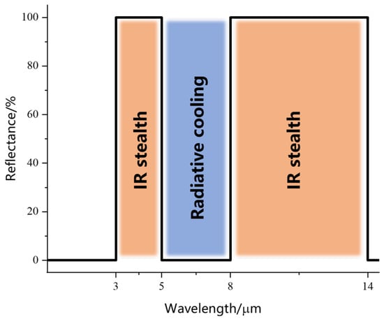
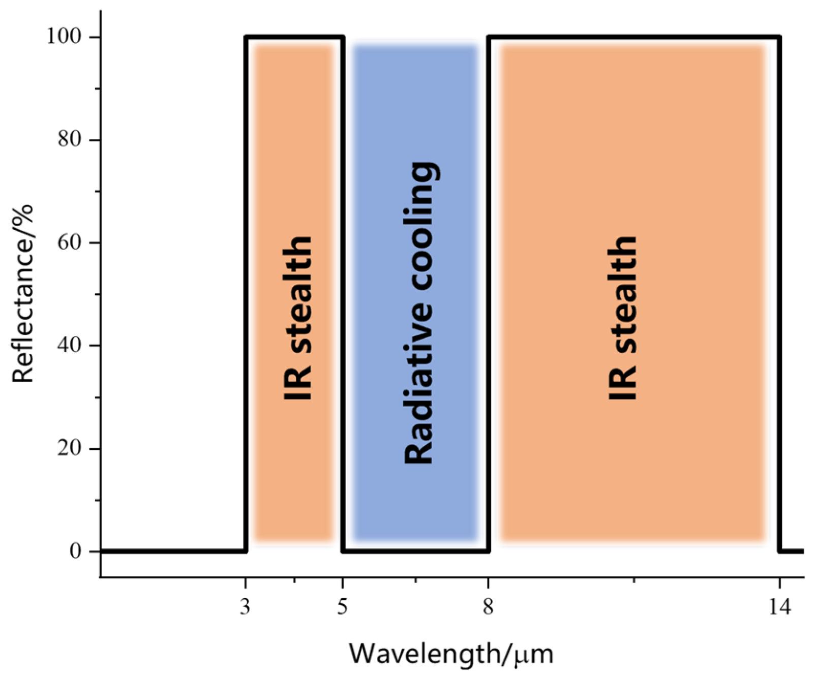
The optimal reflection spectrum of the multilayer thin film is shown in Figure 1. The design objective is to maximize the reflectance in the mid-infrared band (3–5 µm) and the long-wave infrared band (8–14 µm), i.e., to achieve low emissivity for infrared stealth, while minimizing the reflectance in the non-detection band (5–8 µm), i.e., to achieve high emissivity for radiative cooling.
Figure 1.
Optimal reflection spectrum.
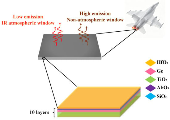
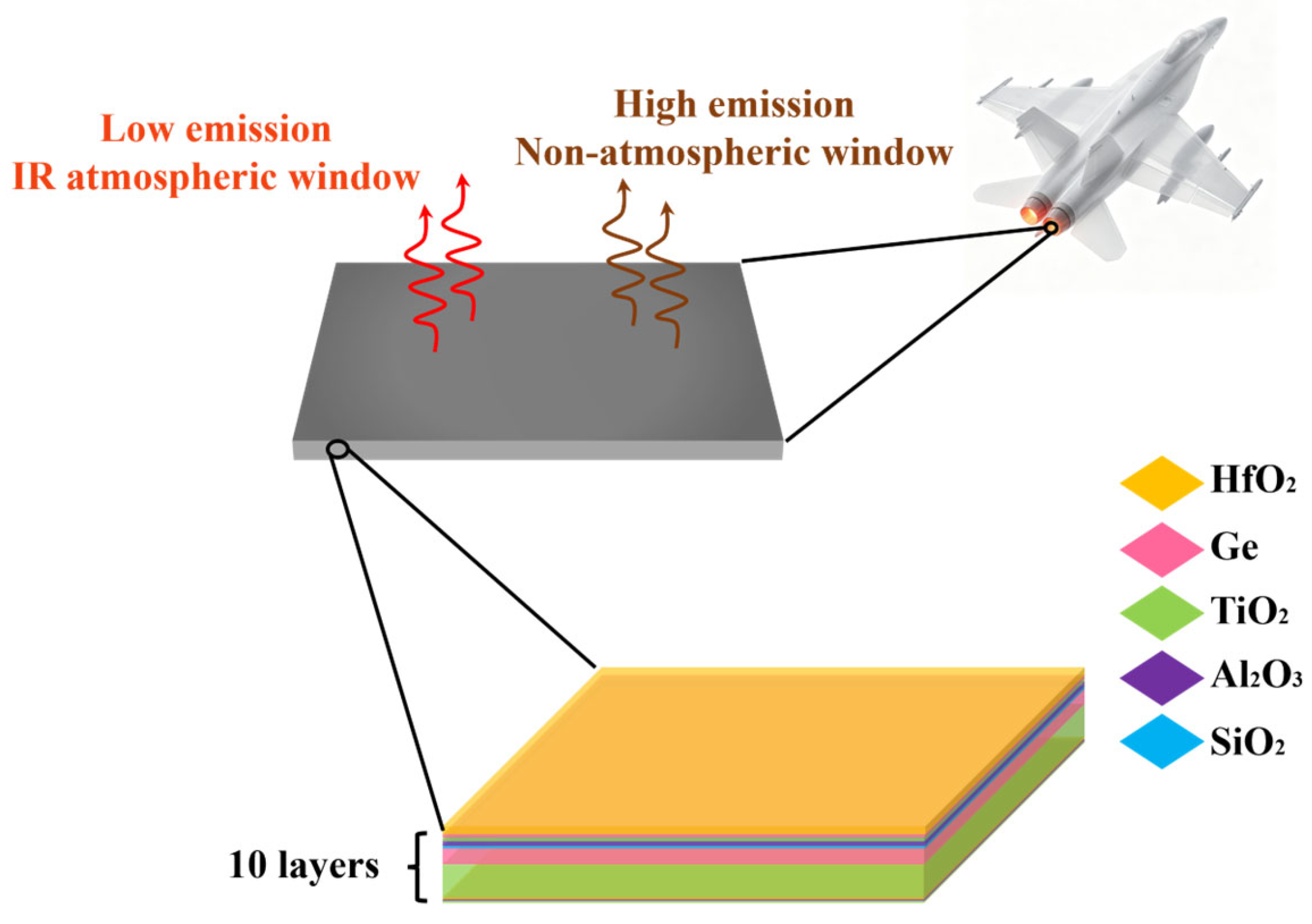
The multilayer thin film structure designed in this work is shown in Figure 2. The film consists of ten layers constructed from five materials: TiO2, Al2O3, HfO2, Ge, and SiO2. The designed thickness of each layer is determined through multiple optimization iterations using the aforementioned transfer matrix method in accordance with the optimal spectral design objective. The specific thickness and positional arrangement of each layer are listed in Table 1.
Figure 2.
Schematic diagram of the multilayer film.
Table 1.
Thickness parameters of the layer material.
The selection of the five materials was guided by multiple criteria. First, a sufficient refractive index contrast is required to establish strong thin-film interference; Ge and TiO2 were chosen as high-index materials (n ≈ 4.0 and 2.4, respectively), while SiO2 and Al2O3 serve as low-index materials (n ≈ 1.45 and 1.7, respectively). Second, all selected materials possess high melting points and good thermal stability for operation at temperatures up to 500 °C. Third, the coefficients of thermal expansion are reasonably matched to minimize interfacial stress during thermal cycling. Fourth, HfO2 was selected as the top encapsulation layer owing to its excellent chemical inertness and oxidation resistance. Finally, all five materials are compatible with electron-beam evaporation deposition, ensuring practical fabrication feasibility.
2.2. Sample Preparation
The total thickness of the ten-layer functional stack is 3410.22 nm (approximately 3.41 µm), as calculated from the individual layer thicknesses listed in Table 1. The physical sample of the multilayer thin film was fabricated by vacuum electron beam evaporation deposition. The film can be deposited on various substrates as required; considering the convenience of subsequent performance testing and the requirements for microstructural characterization, a silicon wafer was selected as the substrate in this work. The silicon wafer was processed following a standard cleaning procedure and then placed into the vacuum chamber. After evacuating the chamber to a vacuum level of 5 × 10⁻⁴ Pa, the layer materials were deposited sequentially. The deposition rate of each material is listed in Table 2. After the deposition of the final layer, substrate heating was maintained for approximately 10 min. The substrate heater was then turned off, and the sample was allowed to cool naturally to room temperature in a vacuum before the chamber was backfilled with air and the sample was retrieved, thereby preventing oxidation or cracking of the film.
Table 2.
The deposition rate of the layer material.
2.3. Experimental Characterization
High-temperature spectral emissivity measurements were performed using a Fourier transform infrared spectrometer coupled with a custom-built vacuum heating chamber. The sample was mounted on a boron nitride heater with an embedded K-type thermocouple, and the surface temperature was independently calibrated using a two-color infrared pyrometer (accuracy ±5 °C at 500 °C). The spectral emissivity was determined via the radiation comparison method: at each temperature, the spectral radiance of the sample was measured and ratioed to that of a reference blackbody cavity at the same temperature, after subtracting the background radiation from the chamber walls and heater [25]. At each setpoint, the sample was held for 30 min to ensure thermal equilibrium, and each spectrum was averaged over 64 scans at a resolution of 4 cm−1.
3. Results and Discussion
3.1. Microstructure and Room-Temperature Infrared Performance
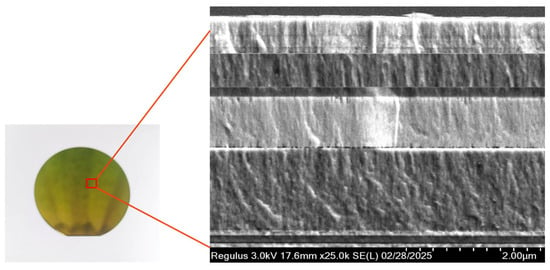
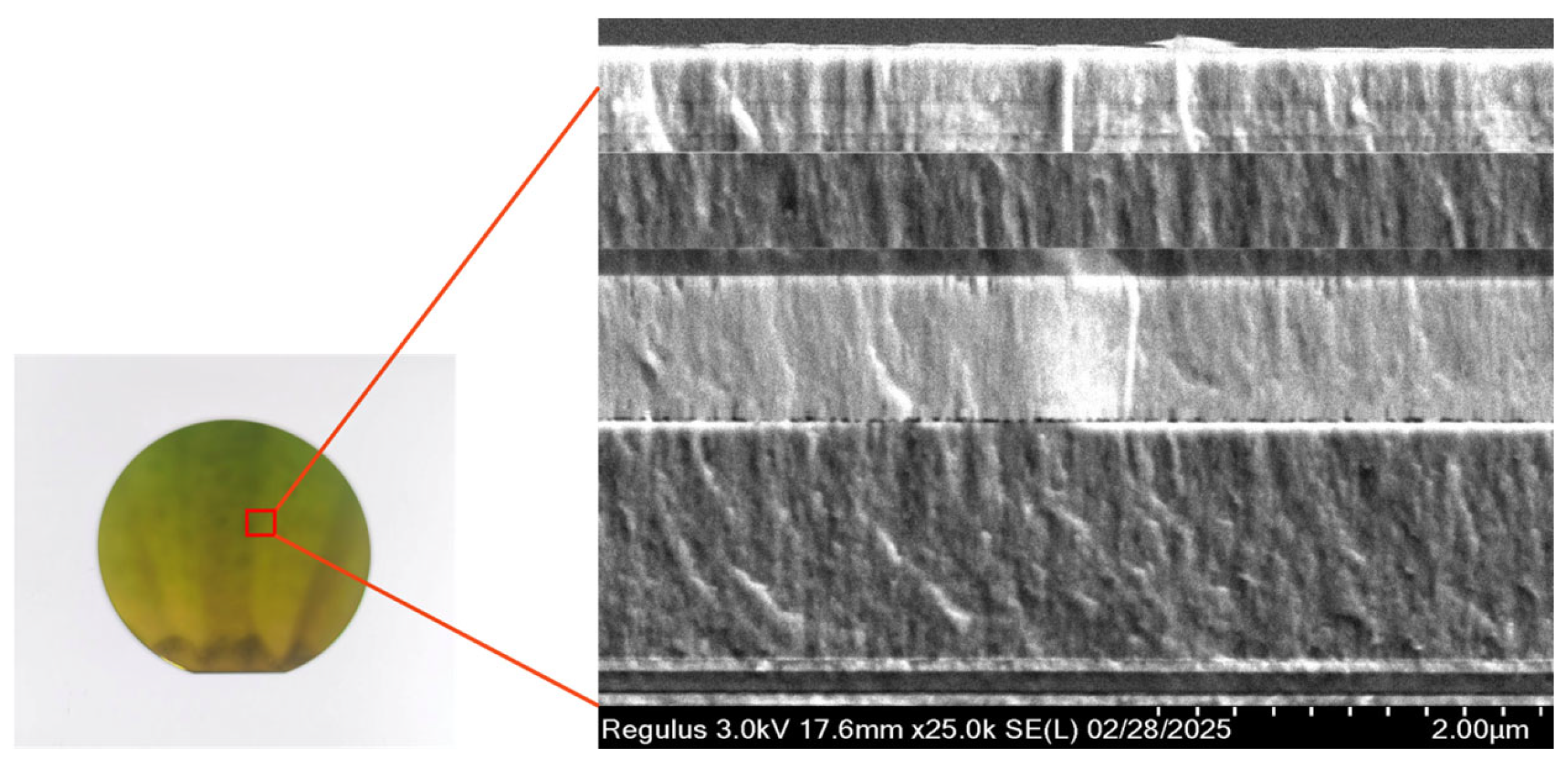
After fabrication, a physical sample of the multilayer thin film was obtained. The surface morphology and cross-sectional microstructure of the sample are shown in Figure 3.
Figure 3.
Surface morphology and microstructure image of the sample.
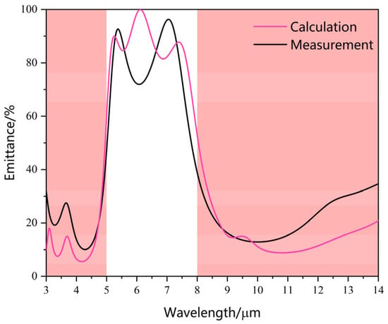
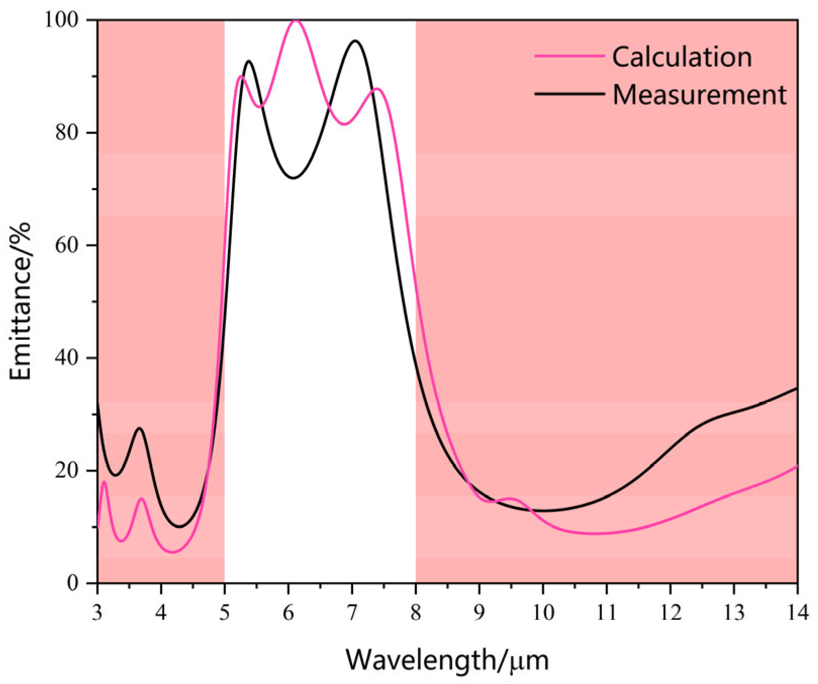
The visible-light photograph reveals that the film sample exhibits an intact, smooth, and clean surface with no signs of peeling or cracking. The scanning electron microscopy (SEM) image shows that the film structure possesses well-defined layers, and the thickness variation is consistent with the design scheme, with the actual thickness values closely matching the theoretically designed values. Subsequently, the spectral characteristics of the sample at room temperature were measured using a Fourier transform infrared (FTIR) spectrometer, and the results are presented in Figure 4.
Figure 4.
Simulated and measured emittance of the multilayer film.
In the figure, the pink curve represents the theoretical simulation result of the spectral emissivity of the multilayer film structure, while the black curve represents the experimental measurement result. The calculated average emissivities are as follows: in the mid-infrared band (3–5 µm), the theoretical value is 0.136 and the experimental value is 0.199; in the long-wave infrared band (8–14 µm), the theoretical value is 0.157 and the experimental value is 0.219; and in the non-detection band (5–8 µm), the theoretical value is 0.852 and the experimental value is 0.774. Although the experimental average emissivities in the mid- and long-wave infrared bands are higher than the theoretical values, all of them remain below 0.23, indicating that the film exhibits favorable infrared stealth performance at room temperature. The experimental average emissivity in the non-detection band is lower than the theoretical value, but the difference between the two is small, and the film still demonstrates favorable heat dissipation performance in practice.
It is worth noting that at approximately 6.5 µm, the simulated spectrum exhibits a local peak while the measured spectrum shows a local trough. This discrepancy is attributed to a combination of factors: (i) residual atmospheric absorption by water vapor and CO2 near 6.2–6.5 µm in the FTIR measurement, which can introduce a systematic depression despite background subtraction; (ii) deviation of the actual optical constants of electron-beam-evaporated amorphous Ge from tabulated values, particularly near its multiphonon absorption edge in the 5–8 µm region, which shifts the interference fringe positions; (iii) film stress-induced thickness non-uniformity in the thicker Ge and TiO2 layers; and (iv) minor interfacial diffusion not accounted for in the ideal simulation. A sensitivity analysis confirms that a 3–5% deviation in the Ge refractive index shifts the interference fringes by 0.3–1.0 µm, sufficient to alter the local trend at 6.5 µm.
The discrepancy between the experimental and designed performance is mainly attributed to two factors. First, during the actual fabrication of the sample, thickness errors arise because the instrument cannot precisely control the layer thickness; these errors accumulate layer by layer, ultimately causing a deviation in the overall performance of the film. It is worth noting that thickness errors have a particularly significant impact on the performance of film structures containing ultrathin metal layers. This is because the designed thickness of ultrathin metal layers typically ranges from a few nanometers to over ten nanometers, and even a slight error can substantially alter the actual thickness, thereby affecting the performance. The multilayer film structure proposed in this work was designed with full consideration of the balance between fabrication feasibility and performance, and appropriate layer thicknesses and materials were ultimately determined. Second, the refractive indices of the layer materials used in the fabricated sample may deviate from the theoretical refractive indices employed in the simulation, which also contributes to the performance discrepancy.
To quantitatively assess the fabrication tolerance, we performed a systematic thickness variation analysis. When all layer thicknesses are uniformly varied by ±5%, the MWIR and LWIR emissivities change by ±12% and ±10%, respectively; for ±10% variation, the changes are ±23% and ±19%; and for ±15% variation, the changes are ±34% and ±28%. A Monte Carlo simulation with independent random thickness errors of ±5% per layer (1000 trials) yields a standard deviation of ~18% in the MWIR emissivity and ~15% in the LWIR emissivity, with 95th-percentile deviations of ~35% and ~29%, respectively, consistent with the observed deviations. The LWIR deviations are slightly smaller owing to the longer wavelengths. The remaining discrepancy is attributed to the refractive index deviation of electron-beam-evaporated Ge films (at 3–5% lower than bulk values due to porosity), which alone can cause an 8–10% increase in the MWIR emissivity and 6–8% increase in the LWIR emissivity. It should be noted that while the proposed structure is not “insensitive” to thickness errors, it exhibits a more predictable and approximately linear response compared to metal-containing structures, where, for example, a ±2 nm error in the 7 nm Ag layer of the Ag/ZnS/Si/Ag/Si emitter reported by Qian et al. [18] causes a 20–35% change in the MWIR emissivity and a 15–25% change in the LWIR emissivity (transfer-matrix calculation), with potentially larger variations in actual discontinuous Ag films near the percolation threshold.
3.2. High-Temperature Infrared Performance
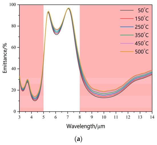
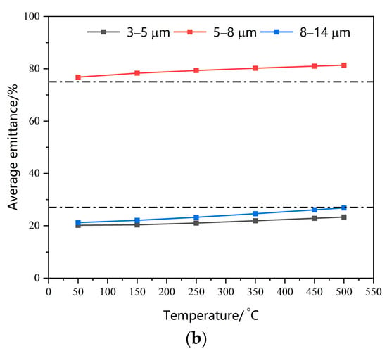
The infrared performance of the multilayer film sample at elevated temperatures was measured using an optical platform coupled with a spectrometer. The heating temperature was increased sequentially to six high-temperature settings: 50 °C, 150 °C, 250 °C, 350 °C, 450 °C, and 500 °C. The spectral emissivity at each temperature was investigated, and the average emissivities in different bands were calculated; the results are shown in Figure 5a,b.
Figure 5.
(a) Measured spectral emittance of the multilayer film at different temperatures; (b) average emittance across different bands.
As can be seen from Figure 5a, the spectral emissivity at different temperatures overall maintains selective radiation characteristics similar to those at room temperature. This indicates that, under high-temperature conditions, the multilayer film still possesses low emissivity in the mid- and long-wave infrared bands and high emissivity in the non-detection band. As observed in Figure 5b, with increasing temperature, the average emissivities in all bands increase slightly, but the increments are small; the average emissivities in the mid- and long-wave infrared bands remain below 0.27, and those in the non-detection band remain above 0.75, demonstrating that the multilayer film can still maintain favorable infrared performance at high temperatures.
It should be noted that the present high-temperature tests were conducted under sequential isothermal heating conditions; systematic thermal cycling tests and long-term aging experiments were not performed in this study. Nevertheless, several factors support the long-term stability of the proposed structure. First, all constituent oxides possess high Tamman temperatures (>1000 °C) and low interdiffusion coefficients at temperatures below 500 °C, and the HfO2 top layer serves as a protective encapsulation against oxidation and interlayer diffusion [26,27]. Second, the potential crystallization of the amorphous Ge layers and its impact on the optical performance are analyzed in detail below. Future work will include systematic thermal cycling, prolonged isothermal exposure, and detailed microstructural characterization to fully evaluate the long-term durability of the film for practical high-temperature applications.
As noted above, the crystallization of the amorphous Ge layers is the primary microstructural concern for high-temperature operation. Akl et al. [28] reported that 790 nm PVD Ge films—nearly identical to our 779.2 nm layer—crystallize at 450–500 °C upon 30 min annealing in air, with the refractive index decreasing from 5.18 to 4.80 (a 7.3% reduction) and the band gap from 0.86 to 0.65 eV. Khan et al. [29] reported similar crystallization in thinner (~110 nm) electron-beam-evaporated Ge films, comparable to our 150.13 nm layer, with severe oxidation at 500 °C in air; their reported band-gap widening (1.1 → 1.35 eV) arises from quantum confinement in 8–20 nm nanocrystals and is not directly applicable to our 150.13 nm layer, which is far thicker than the quantum-confinement regime. The 7.3% refractive index decrease upon crystallization, however, is relevant for both Ge layers.
In contrast to these air-annealed free-standing films, our high-temperature tests were performed in vacuum where Ge oxidation is suppressed, and both Ge layers are sandwiched between dielectric layers rather than exposed at a free surface. These differences—including the elimination of oxidation-induced nucleation sites and the introduction of interface constraints from thermal-expansion mismatch—may influence the crystallization kinetics compared with the cited studies.
To assess the potential impact of full Ge crystallization, a room-temperature transfer-matrix simulation was performed in which the refractive index of both Ge layers was reduced by 7.3% (from the as-deposited amorphous value to the fully nanocrystalline value). The results indicate that complete crystallization would increase the MWIR emissivity by 25–35% and the LWIR emissivity by 15–25%, with the thicker 779.2 nm layer dominating the optical response due to its larger optical thickness.
Experimentally, the in situ emissivity at 500 °C increases by approximately 36% in the MWIR (from 0.199 to below 0.27) and 23% in the LWIR (from 0.219 to below 0.27) relative to the room-temperature values. This increase includes two physically distinct contributions: (i) the reversible thermo-optic effect—the temperature dependence of the refractive indices of all layers—which dominates the in situ measurement and recovers upon cooling; and (ii) an irreversible component due to Ge crystallization, which persists after cooling.
To separate these contributions, the sample was heated to 500 °C, held for 30 min, and then naturally cooled to room temperature in vacuum before re-measurement. The post-heating room-temperature emissivities were 0.205 (MWIR), 0.224 (LWIR), and 0.768 (5–8 µm), representing cumulative changes of +3.0%, +2.3%, and −0.8%, respectively, relative to the pre-heating values (0.199, 0.219, and 0.774). These small cumulative changes indicate that the majority of the high-temperature spectral variation is reversible (thermo-optic effect), while a small irreversible component likely reflects partial Ge crystallization. Comparing the observed cumulative MWIR change (+3.0%) with the simulated full-crystallization impact (+25–35%) suggests a crystalline fraction of approximately 10% under the tested conditions.
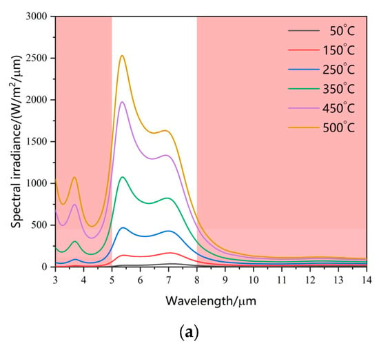
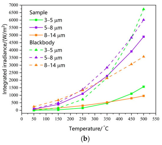
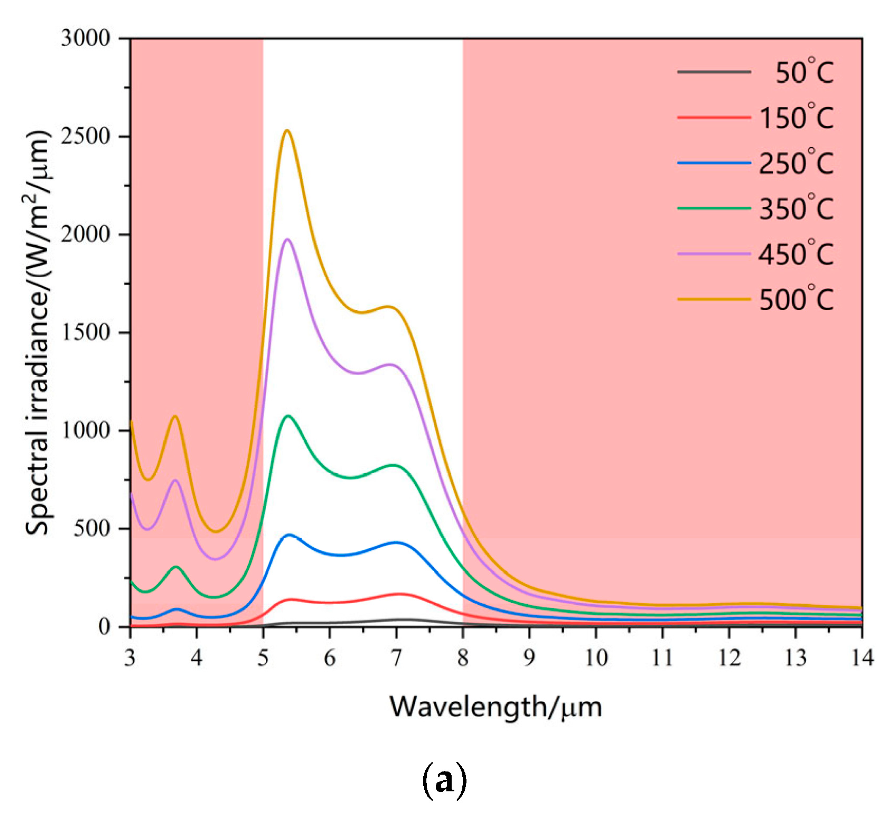
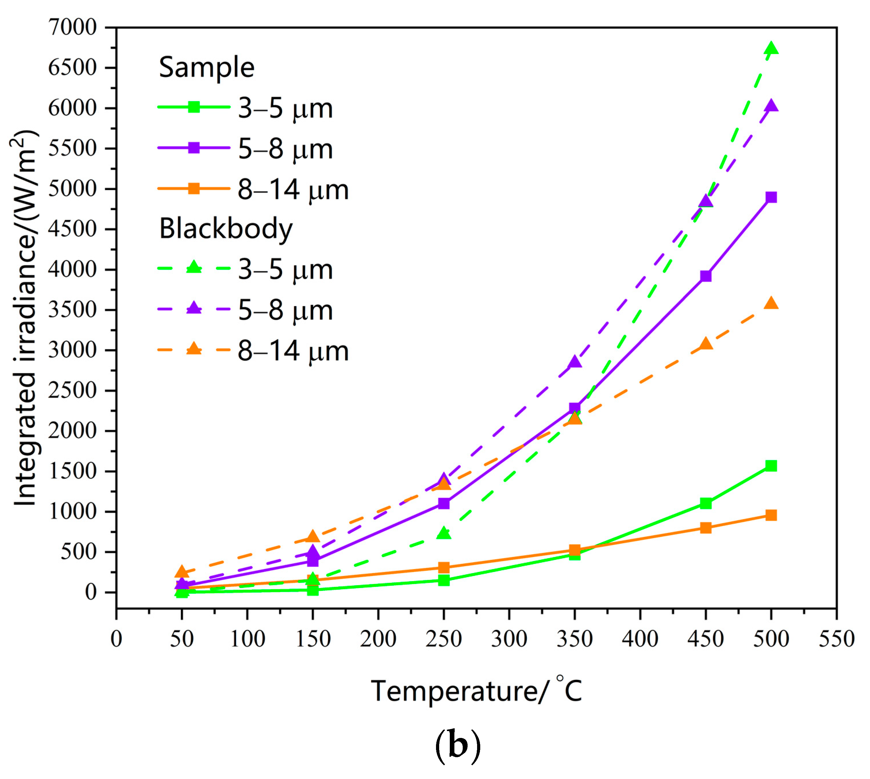
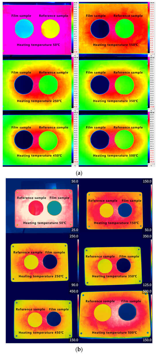
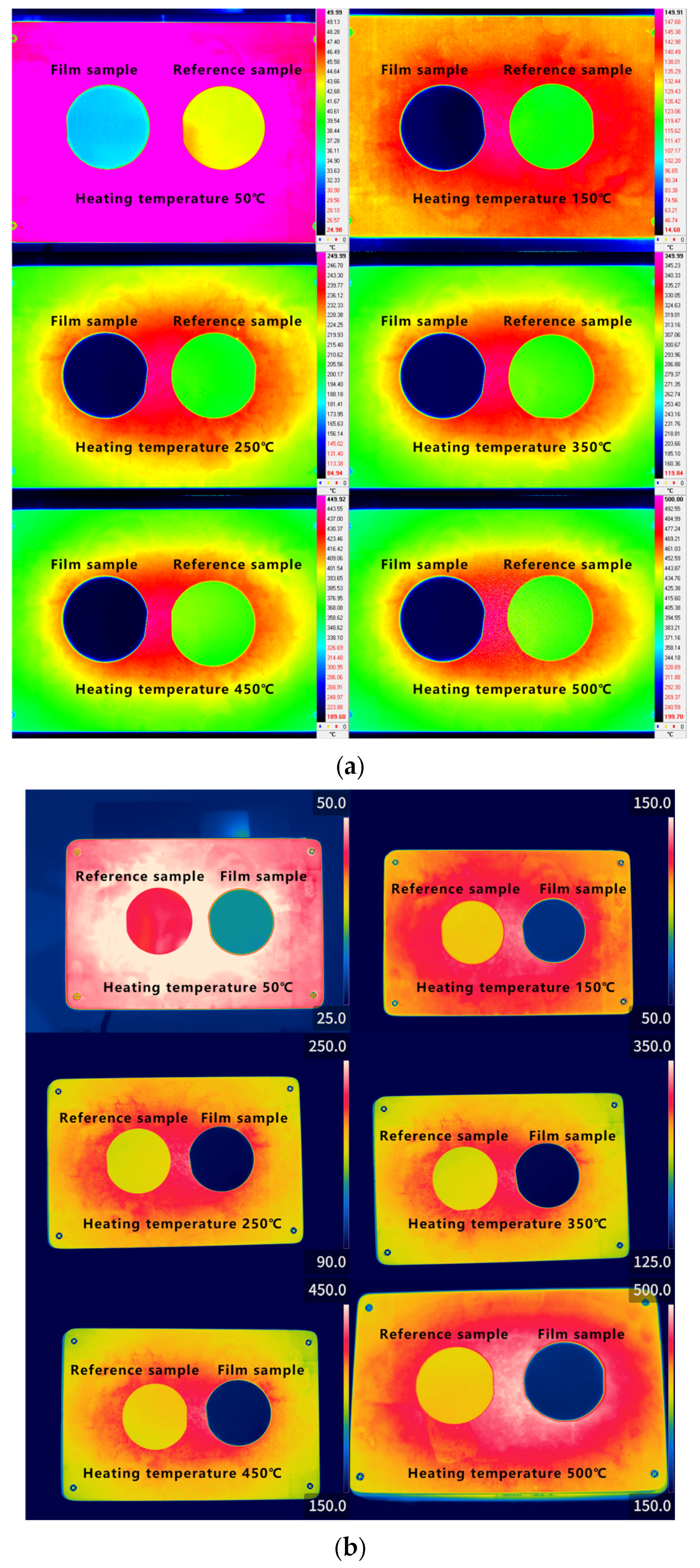
Figure 6a presents the spectral irradiance of the film at different temperatures, which was calculated from the results in Figure 5a. It can be observed that the spectral irradiance of the film increases rapidly with rising temperature overall, with a particularly pronounced increase in the non-detection band. Figure 6b shows the integrated irradiance of the film in different bands at the corresponding temperatures, compared with the integrated irradiance of a standard blackbody in the same bands at the same temperatures. The integrated irradiance of the blackbody exceeds that of the film structure in all bands, and the difference between the two gradually increases with rising temperature. In the non-detection band, the difference in integrated irradiance between the blackbody and the film at the same temperature is relatively the smallest. To further demonstrate the stealth and heat dissipation performance of the multilayer film from multiple perspectives, mid- and long-wave infrared thermal imagers were used to capture the radiation of the film at the aforementioned temperatures, with a high-emissivity reference sample included for comparison; the results are shown in Figure 7a,b.
Figure 6.
(a) Spectral irradiance of the multilayer film at different temperatures; (b) integrated irradiance across different bands.
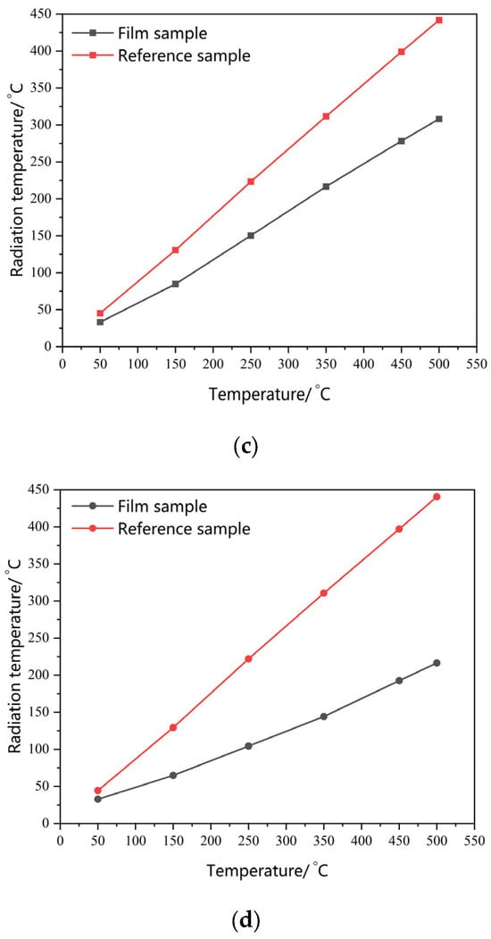
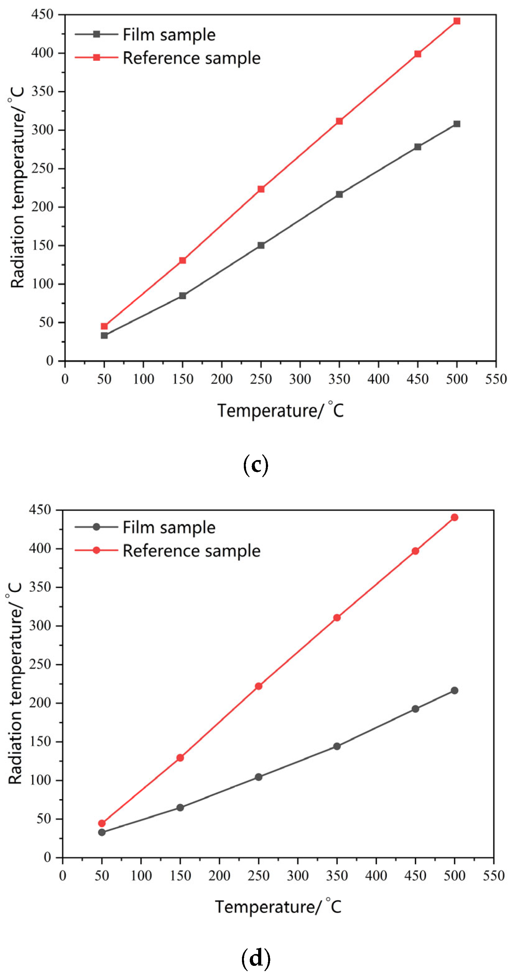
Figure 7.
(a) Thermal images in the mid-infrared band; (b) thermal images in the long-wave infrared band; (c) radiation temperature in the mid-infrared band; (d) radiation temperature in the long-wave infrared band.
Figure 7a,b correspond to the thermal images in the mid-infrared and long-wave infrared bands, respectively. Clearly, under various high-temperature environments, the color difference between the film sample and the reference sample is distinct. Owing to its low infrared emissivity, the radiation temperature of the film sample is consistently lower than that of the reference sample, demonstrating favorable infrared stealth performance. The variation trends of the radiation temperature with the heating temperature in the mid- and long-wave infrared bands are plotted in Figure 7c and Figure 7d, respectively. As is evident from the results, with increasing heating temperature, the radiation temperature in both bands exhibits a rising trend consistent with that observed in the thermal images. Meanwhile, the rate of temperature increase in the film sample is lower than that of the reference sample, reflecting favorable heat dissipation performance.
3.3. Radar Wave-Transmission Performance
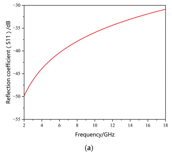
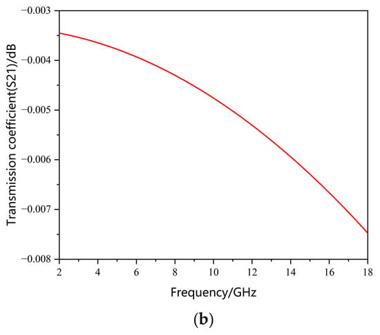
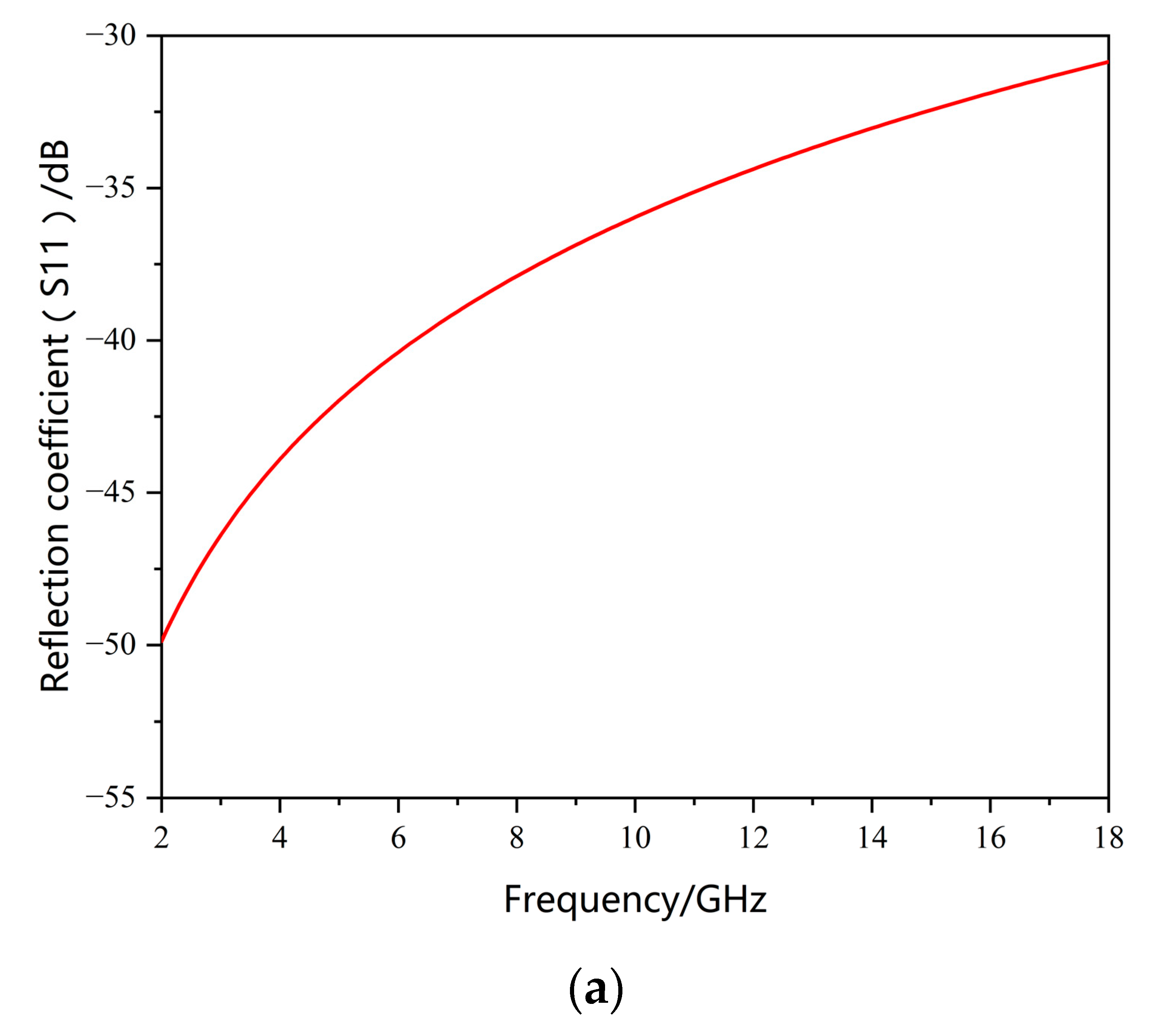
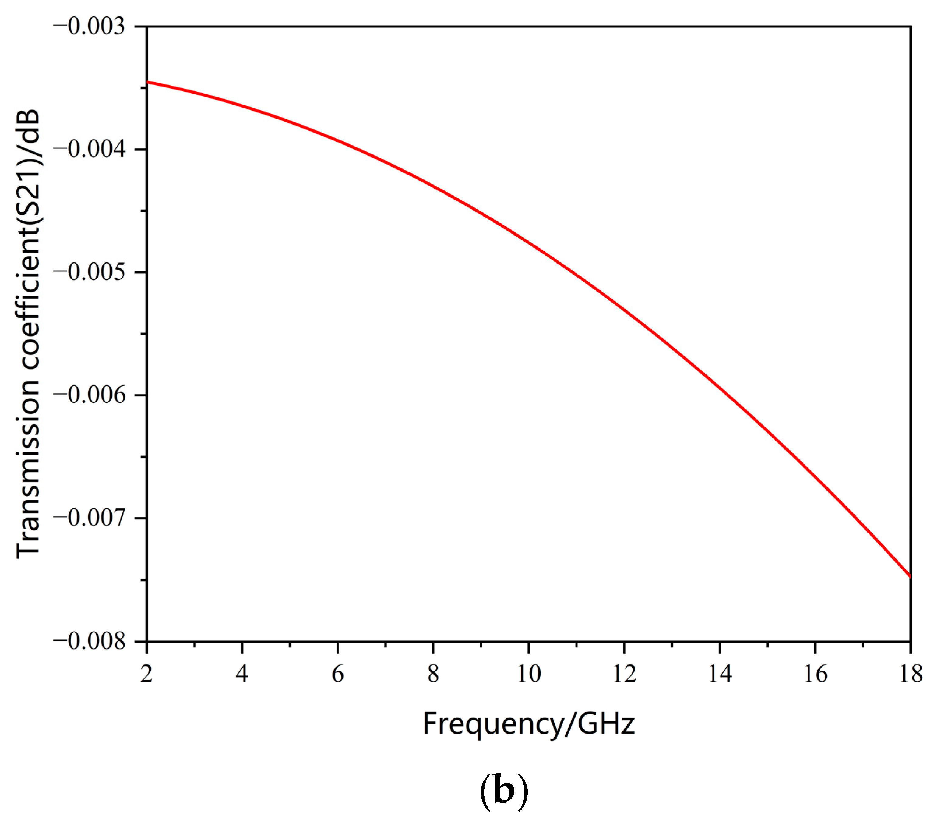
Similar to infrared reconnaissance, radar reconnaissance is also one of the most widely applied measures [30,31,32,33,34,35]. In numerous studies on high-temperature-resistant selective thermal emitters, the film structures generally contain ultrathin metal layers, which serve as the functional layers closely related to the infrared stealth performance. As mentioned above, film structures containing ultrathin metal layers are highly susceptible to thickness errors in their infrared performance and, moreover, impair radar-wave transmission. The multilayer film structure proposed in this work contains no metal layers and can subsequently be integrated with radar-absorbing materials to form compatible stealth materials, achieving multiband stealth performance under high-temperature conditions. The theoretical radar-wave transmission performance of the proposed film structure was simulated, and the resulting curves of the reflection coefficient and transmission coefficient are shown in Figure 8.
Figure 8.
(a) Simulated reflection coefficient; (b) simulated transmission coefficient.
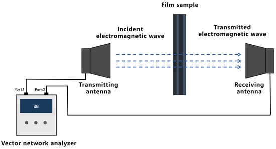
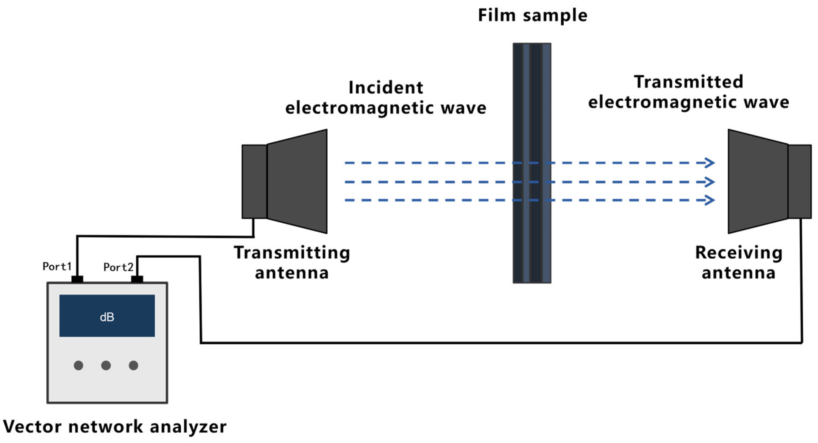
Figure 8a presents the reflection coefficient curve of the multilayer film, and Figure 8b presents the transmission coefficient curve; both are simulated over the 2–18 GHz band. Clearly, both the reflection coefficient and the transmission coefficient exhibit smooth, monotonic variations over the 2–18 GHz band, with the reflection coefficient gradually increasing and the transmission coefficient gradually decreasing as the frequency increases. The minimum reflection coefficient occurs at 2 GHz, with a value of −49.8736 dB, corresponding to a reflectance of 0.00103%, while the maximum occurs at 18 GHz, with a value of −30.8572 dB, corresponding to a reflectance of 0.0821%. The minimum transmission coefficient occurs at 18 GHz, with a value of −0.00747 dB, corresponding to a transmittance of 99.828%, while the maximum occurs at 2 GHz, with a value of −0.00345 dB, corresponding to a transmittance of 99.921%. These results indicate that the multilayer film exhibits extremely weak reflection of radar waves and a transmission performance close to the ideal state. The radar-wave transmission performance of the multilayer film was experimentally measured using a vector network analyzer, and the measurement configuration is shown in Figure 9.
Figure 9.
Scheme of radar performance testing.
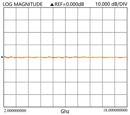
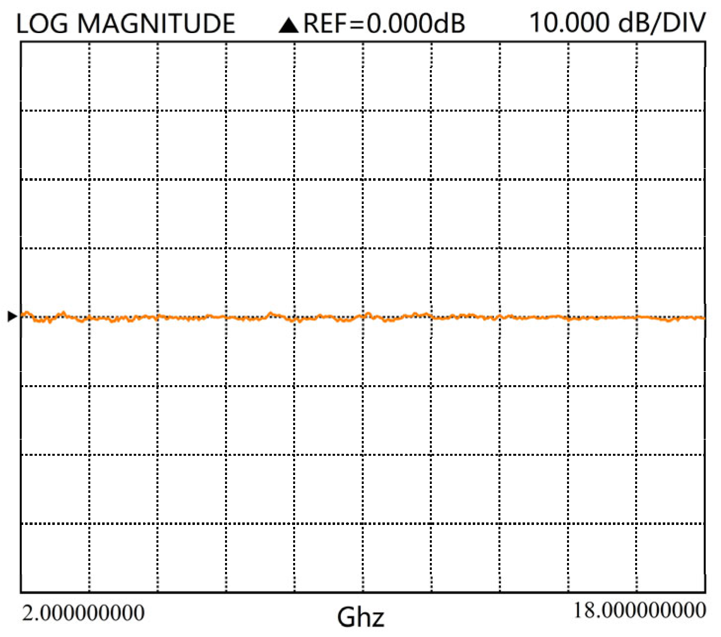
The electromagnetic wave emitted from the transmitting antenna reaches the multilayer film, where a portion is reflected, a portion is absorbed, and the remaining portion transmits through the film structure to the receiving antenna. After internal processing and calculation by the instrument, the actual transmission performance of the film sample is obtained, as shown in Figure 10. The measurement results show that the S21 curve essentially coincides with the reference level, with minimal loss, confirming that the film sample possesses favorable radar-wave transmission performance.
Figure 10.
Measured transmission coefficient.
Quantitatively, the simulated S11 exhibits a mean value of −37.6 dB across the 2–18 GHz frequency band (corresponding to an average reflectance of approximately 0.017%). The simulated S21 demonstrates minimal variation, with an average insertion loss of merely 0.0052 dB (average transmittance ≈ 99.88%). Experimentally measured S21 values indicate an average insertion loss of less than 0.1 dB within the 2–18 GHz band (average transmittance > 97.7%). This ultra-low insertion loss ensures that the thin film can be integrated with radar-absorbing materials without significantly compromising their absorption performance [36,37].
To assess the compatibility of the proposed film with radar-absorbing materials (RAMs), we note that the infrared and microwave responses are inherently decoupled owing to the large difference in penetration depth. Infrared radiation (3–14 µm) interacts only with the top multilayer film (skin depth ~micrometers) and does not reach the underlying RAM, whereas microwave radiation (2–18 GHz) penetrates through the electrically thin dielectric film into the RAM. A preliminary transfer-matrix calculation with an absorbing substrate (infrared reflectance = 0.5) beneath the film confirms that the band-averaged infrared emissivities change by less than 2% compared to the standalone film. Experimental verification with actual RAMs will be conducted in future work.
To quantitatively evaluate the advancement of the proposed design over the state of the art, we propose a combined figure-of-merit (FOM) integrating stealth efficiency, heat dissipation, and radar transparency: FOM = (ε_cooling/ε_stealth) × T_radar, where ε_cooling is the 5–8 µm emissivity, ε_stealth is the average MWIR and LWIR emissivity, and T_radar is the average 2–18 GHz transmittance. Table 3 compares the proposed work with representative metal-containing multilayer selective emitters. The radar transmittance values for the metal-containing structures are estimated based on the standard transmission-line model for ultrathin metal films. The proposed all-dielectric design achieves a combined FOM of approximately 3.6, compared to 0.20–0.24 for metal-containing structures. The ε_cooling/ε_stealth ratios are comparable across all works (3.70 for this work vs. 4.0–4.78 for prior work), so the FOM improvement arises almost entirely from the exceptional radar transparency (>97.7% vs. <5%).
Table 3.
The comparison of the proposed work with representative multilayer film selective thermal emitters.
In terms of insertion loss, the samples reported by Fu et al. [17] and Qian et al. [18] exhibited estimated insertion losses exceeding 13 dB. In contrast, the measured average insertion loss of the sample proposed in this work is less than 0.1 dB across the 2–18 GHz frequency band. Consequently, the insertion loss of the proposed all-dielectric thin film is more than two orders of magnitude lower (i.e., over 130 times lower) than that of metal-containing structures. This significant improvement arises because free electrons in metallic layers cause strong absorption and reflection of electromagnetic waves in the microwave regime, whereas dielectric materials, lacking free carriers, are inherently transparent to microwave radiation.
4. Conclusions
In summary, a novel high-temperature-resistant selective thermal emitter based on a multilayer thin film is proposed in this work. Compared with film structures containing ultrathin metal layers, the proposed all-dielectric structure exhibits a more predictable and approximately linear response to thickness errors compared with metal-containing structures, owing to the absence of ultrathin critical layers, and is more fabrication-friendly. Meanwhile, owing to the absence of metal layers, the film exhibits excellent radar-wave transmission performance and can subsequently be integrated with radar-absorbing materials to achieve compatible stealth [38,39,40,41]. Through computational simulation and performance testing, the multilayer film exhibits an average emissivity of 0.199 in the mid-infrared band and 0.219 in the long-wave infrared band at room temperature, demonstrating favorable infrared stealth performance; its average emissivity in the non-detection band is 0.774, demonstrating favorable heat dissipation performance. Under various high-temperature conditions up to 500 °C, the film still maintains selective radiation characteristics similar to those at room temperature, indicating that infrared stealth and radiative cooling can be achieved at high temperatures. The film possesses broad application prospects and provides a new scheme for the realization of high-temperature-resistant selective thermal emitters.
Author Contributions
Conceptualization, C.D. and J.S.; methodology, C.D.; software, Z.L.; validation, D.Z. and C.D.; formal analysis, Z.C.; investigation, X.L.; resources, C.D.; data curation, Z.L.; writing—original draft preparation, C.D.; writing—review and editing, C.D.; visualization, Z.L.; supervision, J.S.; project administration, J.Z.; funding acquisition, J.S. All authors have read and agreed to the published version of the manuscript.
Funding
This research was funded by Hunan Provincial Innovation Foundation for Postgraduate, grant number XJJC2025074.
Institutional Review Board Statement
Not applicable.
Informed Consent Statement
Not applicable.
Data Availability Statement
The data presented in this study are available on request from the corresponding author.
Conflicts of Interest
The authors declare no conflicts of interest.
References
- Raman, A.P.; Anoma, M.A.; Zhu, L.; Rephaeli, E.; Fan, S. Passive radiative cooling below ambient air temperature under direct sunlight. Nature 2014, 515, 540–544. [Google Scholar] [CrossRef] [Scilit]
- Zhu, H.; Li, Q.; Zheng, C.; Hong, Y.; Xu, Z.; Wang, H.; Shen, W.; Kaur, S.; Ghosh, P.; Qiu, M. High-temperature infrared camouflage with efficient thermal management. Light Sci. Appl. 2020, 9, 63. [Google Scholar] [CrossRef] [Scilit]
- Zhu, H.; Li, Q.; Tao, C.; Hong, Y.; Xu, Z.; Shen, W.; Kaur, S.; Ghosh, P.; Qiu, M. Multispectral camouflage for infrared, visible, lasers and microwave with radiative cooling. Nat. Commun. 2021, 12, 1805. [Google Scholar] [CrossRef] [Scilit]
- Peng, L.; Liu, D.; Cheng, H.; Zhou, S.; Zu, M. A multilayer film based selective thermal emitter for infrared stealth technology. Adv. Opt. Mater. 2018, 6, 1801006. [Google Scholar] [CrossRef] [Scilit]
- Fan, S.; Li, W. Photonics and thermodynamics concepts in radiative cooling. Nat. Photonics 2022, 16, 182–190. [Google Scholar] [CrossRef] [Scilit]
- Lee, M.; Kim, G.; Jung, Y.; Pyun, K.R.; Lee, J.; Kim, B.; Ko, S.H. Photonic structures in radiative cooling. Light Sci. Appl. 2023, 12, 144. [Google Scholar] [CrossRef] [Scilit]
- Yu, K.; Zhang, W.; Qian, M.; Shen, P.; Liu, Y. Multiband metamaterial emitters for infrared and laser compatible stealth with thermal management based on dissipative dielectrics. Photonics Res. 2023, 11, 290–298. [Google Scholar] [CrossRef] [Scilit]
- Qin, B.; Zhu, Y.; Zhou, Y.; Qiu, M.; Li, Q. Whole-infrared-band camouflage with dual-band radiative heat dissipation. Light Sci. Appl. 2023, 12, 220. [Google Scholar] [CrossRef] [Scilit]
- Zhong, S.; Wu, L.; Liu, T.; Huang, J.; Jiang, W.; Ma, Y. Transparent transmission-selective radar-infrared bi-stealth structure. Opt. Express 2018, 26, 16466–16476. [Google Scholar] [CrossRef] [Scilit]
- Zhang, T.; Duan, Y.; Liu, J.; Lei, H.; Sun, J.; Pang, H.; Huang, L. Asymmetric electric field distribution enhanced hierarchical metamaterials for radar-infrared compatible camouflage. J. Mater. Sci. Technol. 2023, 146, 10–18. [Google Scholar] [CrossRef] [Scilit]
- Park, C.; Kim, J.; Hahn, J.W. Selective emitter with engineered anisotropic radiation to minimize dual-band thermal signature for infrared stealth technology. ACS Appl. Mater. Interfaces 2020, 12, 37580–37588. [Google Scholar] [CrossRef] [Scilit]
- Lee, N.; Yoon, B.; Kim, T.; Bae, J.; Lim, J.; Chang, I.; Cho, H.H. Multiple resonance metamaterial emitter for deception of infrared emission with enhanced energy dissipation. ACS Appl. Mater. Interfaces 2020, 12, 8862–8869. [Google Scholar] [CrossRef] [Scilit]
- Jiang, X.; Yuan, H.; He, X.; Du, T.; Ma, H.; Li, X.; Luo, M.; Zhang, Z.; Chen, H.; Yu, Y.; et al. Implementing infrared camouflage with thermal management based on inverse design and hierarchical metamaterial. Nanophotonics 2023, 12, 2511–2522. [Google Scholar] [CrossRef] [Scilit]
- Huang, J.; Wang, Y.; Yuan, L.; Huang, C.; Liao, J.; Ji, C.; Luo, X. Large-area and flexible plasmonic metasurface for laser–infrared compatible camouflage. Laser Photonics Rev. 2023, 17, 2200616. [Google Scholar] [CrossRef] [Scilit]
- Gu, S.; Quan, C.; Liu, P.; Zhu, Z.; Zhang, J. Laser-compatible infrared stealth metamaterial based on high-temperature resistant metal. Infrared Phys. Technol. 2024, 136, 105072. [Google Scholar] [CrossRef] [Scilit]
- Huang, Y.; Zhu, Y.; Qin, B.; Zhou, Y.; Qin, R.; Ghosh, P.; Qiu, M.; Li, Q. Hierarchical visible-infrared-microwave scattering surfaces for multispectral camouflage. Nanophotonics 2023, 12, 1097–1106. [Google Scholar] [CrossRef] [Scilit]
- Fu, Z.-C.; Cheng, Z.-M.; Wang, F.-Q.; Yan, D.; Zhang, X.-P.; Zhang, A.-Y.; Liang, H.-X. A multilayer film based on thin-film interference and impedance matching for dual-laser and infrared stealth as well as thermal management. Optik 2023, 289, 171261. [Google Scholar] [CrossRef] [Scilit]
- Qian, M.; Shi, Q.; Qin, L.; Huang, J.; Guo, C.; Liu, Y.; Yu, K. Fabrication of selective thermal emitter with multilayer films for mid-/low-temperature infrared stealth with radiative cooling. Photonics 2023, 10, 645. [Google Scholar] [CrossRef] [Scilit]
- Kim, T.; Bae, J.-Y.; Lee, N.; Cho, H.H. Hierarchical Metamaterials for Multispectral Camouflage of Infrared and Microwaves. Adv. Funct. Mater. 2019, 29, 1807319. [Google Scholar] [CrossRef] [Scilit]
- Wu, Y.; Luo, J.; Pu, M.; Liu, B.; Jin, J.; Li, X.; Ma, X.; Guo, Y.; Guo, Y.; Luo, X. Optically Transparent Infrared Selective Emitter for Visible-Infrared Compatible Camouflage. Opt. Express 2022, 30, 17259–17269. [Google Scholar] [CrossRef] [Scilit]
- Qin, R.; Zhu, H.; Zhu, R.; Ghosh, P.; Qiu, M.; Li, Q. Multi-Dimensional Camouflage against VIS-NIR Hyperspectral, MIR Intensity, and MIR Polarization Imaging. Light Sci. Appl. 2026, 15, 63. [Google Scholar] [CrossRef] [Scilit]
- Zhu, R.; Zhu, H.; Qin, B.; Yao, W.; Zhao, M.; Yu, N.; Su, Z.; Xie, L.; Ma, H.; Huangfu, J.; et al. Digital Camouflage Encompassing Optical Hyperspectra and Thermal Infrared-Terahertz-Microwave Tri-Bands. Nat. Commun. 2025, 16, 8112. [Google Scholar] [CrossRef] [Scilit]
- Huang, Y.; Zhu, H.; Zhou, Y.; Dai, C.; Zhu, R.; Ghosh, P.; Qiu, M.; Li, Q. Adaptive Visible-Infrared Camouflage with Wide-Range Radiation Control for Extreme Ambient Temperatures. PhotoniX 2025, 6, 25. [Google Scholar] [CrossRef] [Scilit]
- Zhao, M.; Zhu, H.; Qin, B.; Zhu, R.; Zhang, J.; Ghosh, P.; Wang, Z.; Qiu, M.; Li, Q. High-Temperature Stealth across Multi-Infrared and Microwave Bands with Efficient Radiative Thermal Management. Nano-Micro Lett. 2025, 17, 199. [Google Scholar] [CrossRef] [Scilit]
- Gao, S.; Sun, Y.; Xi, L.; He, R.; Kang, X.; Li, Y. Microwave Absorption Optimization via Additive Manufacturing: Process-Dependent Mechanisms of Electromagnetic Attenuation. Carbon 2025, 234, 120795. [Google Scholar] [CrossRef] [Scilit]
- Gao, S.; Dong, H.; Zhang, Y.; Sun, Y.; Yu, C.; Wang, Z.; Zhang, H.; Huang, Y.; Li, Y. Rapid Prediction of Effective Absorption Bandwidth in PEEK/CF Additive Manufacturing Metastructure via Interpretable Machine Learning. J. Mater. Sci. Technol. 2025, 239, 307–319. [Google Scholar] [CrossRef] [Scilit]
- Gao, S.; Sun, Y.; Xi, L.; Zhao, T.; Huang, Y.; He, R.; Kang, X.; Li, Y. Recent Advances in Machine Learning-Assisted Design of Additive Manufacturing Metastructures: A Review. Compos. Struct. 2025, 372, 119525. [Google Scholar] [CrossRef] [Scilit]
- Akl, A.A.; Howari, H. Nanocrystalline Formation and Optical Properties of Germanium Thin Films Prepared by Physical Vapor Deposition. J. Phys. Chem. Solids 2009, 70, 1337–1343. [Google Scholar] [CrossRef] [Scilit]
- Khan, A.F.; Mehmood, M.; Rana, A.M.; Muhammad, T. Effect of Annealing on Structural, Optical and Electrical Properties of Nanostructured Ge Thin Films. Appl. Surf. Sci. 2010, 256, 2031–2037. [Google Scholar] [CrossRef] [Scilit]
- Dang, S.; Ye, H. A visible-infrared-compatible camouflage photonic crystal with heat dissipation by radiation in 5–8 μm. Cell Rep. Phys. Sci. 2021, 2, 100617. [Google Scholar] [CrossRef] [Scilit]
- Chamoli, S.K.; Li, W. Visibly transparent multifunctional camouflage coating with efficient thermal management. Opt. Lett. 2023, 48, 4340–4343. [Google Scholar] [CrossRef] [Scilit]
- Su, Y.; Deng, Z.; Qin, W.; Wang, X.; Gong, R. Adaptive infrared camouflage based on quasi-photonic crystal with Ge2Sb2Te5. Opt. Commun. 2021, 497, 127203. [Google Scholar] [CrossRef] [Scilit]
- Zhang, J.K.; Zhao, D.P.; Chen, Z.S.; Liu, Y.; Wang, H.; Lin, Z.Q.; Shi, J.M. One dimensional photonic crystal based multilayer film with low IR and visible signatures. Opt. Mater. 2019, 91, 261–267. [Google Scholar] [CrossRef] [Scilit]
- Li, Q.; Pang, Y.; Li, Y.; Yan, M.; Wang, J.; Xu, Z.; Qu, S. Low radar cross section checkerboard metasurface with a transmission window. J. Appl. Phys. 2018, 124, 065107. [Google Scholar] [CrossRef] [Scilit]
- Yan, M.; Wang, J.; Wang, W.; Xu, C.; Chen, H.; Wang, W.; Zheng, L.; Qu, S. An FSS-backed reflective polarization conversion meta-surface for radar stealth. Photonics Nanostructures Fundam. Appl. 2020, 39, 100846. [Google Scholar] [CrossRef] [Scilit]
- Dong, H.; Gao, S.; Yu, C.; Huang, Y.; Zhao, T.; Li, Y. Enhancing Microwave Absorption of Bio-Inspired Structure through 3D Printed Concentric Infill Pattern. Compos. Part B Eng. 2025, 289, 111924. [Google Scholar] [CrossRef] [Scilit]
- Gao, S.; Huang, Y.; He, R.; Kang, X.; Li, Y. Comprehensive Unraveling of CT-Derived Defect Characteristics in Fused Deposition Modeling via Machine Learning: Clustering, Classification, Regression and Process Correlation. Compos. Part A Appl. Sci. Manuf. 2026, 197, 109942. [Google Scholar] [CrossRef] [Scilit]
- Meng, Z.; Liu, D.; Wang, J.; Pang, Y.; Liu, T.; Jia, Y.; Gui, B.; Cheng, H. Metamaterial-inspired infrared electrochromic devices with wideband microwave absorption for multispectral camouflage. Photonics Res. 2024, 12, 2435–2446. [Google Scholar] [CrossRef] [Scilit]
- Liu, Z.; Zhou, X.; Chen, J.; Chen, Y.; Xue, W.; Cao, Y. Designed band-pass frequency selective surfaces with thermal transparency. Phys. Lett. A 2021, 406, 127459. [Google Scholar] [CrossRef] [Scilit]
- Chang, Q.; Ji, J.; Chen, K.; Wu, W.; Ma, Y. Transparent and ultra-thin flexible checkerboard metasurface for radar-infrared bi-stealth. Sensors 2024, 24, 1531. [Google Scholar] [CrossRef] [Scilit]
- Gao, Z.; Xu, C.; Tian, X.; Wang, J.; Zhang, H.; Qu, S.; Fan, Q. Multifunctional ultra-thin metasurface with low infrared emissivity, microwave absorption and high optical transmission. Opt. Commun. 2021, 500, 127327. [Google Scholar] [CrossRef] [Scilit]

Disclaimer/Publisher’s Note: The statements, opinions and data contained in all publications are solely those of the individual author(s) and contributor(s) and not of MDPI and/or the editor(s). MDPI and/or the editor(s) disclaim responsibility for any injury to people or property resulting from any ideas, methods, instructions or products referred to in the content. |
© 2026 by the authors. Licensee MDPI, Basel, Switzerland. This article is an open access article distributed under the terms and conditions of the Creative Commons Attribution (CC BY) license.