


Abstract
The development of earth-abundant, low-cost and chemically stable semiconductor absorbers is essential for advancing next-generation photovoltaic technologies. Among the promising candidates, copper–tin sulfide and tin sulfide based chalcogenide materials have attracted considerable attention owing to their suitable optical properties, tunable composition, and compatibility with solution-based deposition techniques. However, a comprehensive understanding of how the composition and the underlying substrate affect the structural, morphological, and optical characteristics of these thin films remains important for their rational integration into photovoltaic device architectures. The aim of this paper was to investigate copper–tin sulfide and tin sulfide thin films, prepared by chemical bath deposition on glass and ITO/glass substrates in order to show the influence of the composition and the substrate nature on their structural, morphological, and optical properties for photovoltaic applications. Thin films of copper–tin sulfide (Cu:Sn molar ratios of 1:1 and 2:1) and tin sulfide were prepared by chemical bath deposition at low temperature under identical conditions and characterized as follows: elemental composition by X-ray fluorescence (XRF), structural ordering by X-ray diffraction (XRD), morphology by atomic force microscopy (AFM), optical properties by spectroscopic ellipsometry (SE), and vibrational modes of components by Raman spectroscopy. The AFM and XRD analyses showed that the Cu-containing films are amorphous, with RMS roughness of 46.0 nm (Cu:Sn = 1:1) and up to 120.5 nm (Cu:Sn = 2:1). Without any thermal treatment, the substrate determines the tin sulfide phase: on glass, hexagonal SnS2 (berndtite) forms as nanoplates a few layers thick (crystallite size ~11–13 nm, RMS roughness 54.8 nm), whereas on ITO/glass, three-dimensional orthorhombic SnS (herzenbergite) crystallites of ~18 nm grow (RMS roughness 47.8 nm). The films show absorption coefficients of (2–5) × 104 cm−1 at 630 nm and optical band gaps between 1.87 and 2.70 eV, which make them candidates for further investigation as absorber layers in solar cells.
1. Introduction
The rapid growth of global energy demand, driven by population growth, industrialization, and technological advancement, has intensified the need for efficient and sustainable energy technologies [1,2,3,4,5,6], and, in this regard, multifunctional materials are among the most investigated candidates for various practical applications [7,8]. Renewable energy sources, including solar, wind, hydroelectric, geothermal, and biomass energy, offer environmentally friendly alternatives capable of reducing greenhouse gas emissions while meeting growing energy demands [9]. Therefore, solar energy has emerged as a promising renewable resource due to its abundance and potential for clean electricity generation. The amount of solar energy reaching the Earth’s surface far exceeds the total global energy consumption, making solar power a promising solution for achieving long-term energy security and carbon neutrality [10,11,12]. Over the past few decades, significant advances have been made in photovoltaic (PV) technologies to improve energy conversion efficiency while reducing production costs [13,14,15,16]. Conventional silicon-based solar cells currently dominate the commercial market; however, their manufacturing processes often require high temperatures, sophisticated fabrication facilities, and substantial energy input, which can increase production costs and limit scalability [17,18]. To address these limitations, the development of efficient solar cells therefore depends strongly on the discovery and optimization of advanced semiconducting light-absorbing materials with suitable optical, electronic, and structural properties [19]. In this context, thin-film solar cells based on semiconductor compounds composed of earth-abundant and relatively low-cost elements have attracted considerable interest [20,21]. In particular, chalcogenide semiconductors offer several advantages, including strong optical absorption, suitable band-gap energies, compositional tunability, and the possibility of fabrication using relatively simple deposition techniques [22,23].
Among the different chalcogenide systems investigated for photovoltaic applications, copper–tin sulfide (Cu–Sn–S) and tin sulfide (SnS) compounds are promising candidates for the development of environmentally benign absorber layers [24]. These materials are composed of relatively abundant elements and exhibit optical and electronic properties suitable for solar-energy conversion. Tin sulfide is particularly attractive because of its appropriate band-gap energy, high absorption coefficient, and chemical stability, while copper–tin sulfide compounds provide additional possibilities for tailoring the structural and optoelectronic properties through control of the Cu:Sn composition [25]. Moreover, both material systems can be prepared by low-cost solution-based methods, making them compatible with potentially scalable thin-film fabrication processes.
The properties of chalcogenide absorber layers are strongly dependent not only on their chemical composition but also on the conditions under which the films are deposited [26]. Variations in the relative concentration of the constituent elements can lead to the formation of different crystalline phases, stoichiometries, defect populations, and surface morphologies, thereby affecting the optical and structural characteristics of the resulting films. In Cu–Sn–S systems, control of the Cu:Sn ratio is therefore particularly important because it can modify phase formation and crystallization behavior and consequently influence the suitability of the films for photovoltaic applications [27,28]. Similarly, for SnS films, the structural quality and surface morphology can significantly affect light absorption and the subsequent charge-generation and transport processes in a photovoltaic device [29]. In addition to composition, the nature of the underlying substrate plays an important role in thin-film growth [30,31]. The substrate can influence nucleation, crystal orientation, grain development, surface roughness, adhesion, and the optical response of the deposited layer [32,33,34,35]. This effect is especially relevant for multilayer photovoltaic architectures, in which the absorber is deposited onto functional layers such as transparent conducting oxides or electron-transport materials [36]. ITO and glass are widely employed in optoelectronic structures because of their electrical and optical properties; however, their different surface and interfacial characteristics may result in distinct nucleation and crystallization mechanisms during chemical deposition [37,38,39,40,41,42,43]. A systematic evaluation of the substrate effect is therefore necessary to establish the appropriate conditions for the growth of high-quality absorber films.
Chemical bath deposition (CBD) is particularly attractive for the preparation of chalcogenide thin films because it is a simple, low-cost, and versatile technique that can operate at relatively low temperatures and over large substrate areas [44,45]. The method allows the deposition parameters and precursor concentrations to be adjusted to control the composition, thickness, morphology, and structural properties of the resulting films. These characteristics make CBD a promising approach for the fabrication of absorber layers intended for cost-effective photovoltaic technologies [46].
Despite the considerable interest in Cu–Sn–S and SnS materials, a comprehensive understanding of the combined effects of composition and substrate on their structural, morphological, and optical properties remains necessary. Comparative studies performed under identical deposition conditions can provide valuable information about the role of the substrate independently of variations in the processing parameters. Such information is important for identifying the conditions that promote crystallization and favorable optical absorption without requiring additional high-temperature treatments.
The present work investigated the influence of film composition and substrate type on the properties of chemically deposited tin-based chalcogenide thin films. Copper–tin sulfide and tin sulfide films were deposited by chemical bath deposition on glass and ITO/glass substrates. The obtained films were characterized in terms of their composition, crystal structure, surface morphology, optical behavior, and vibrational properties using X-ray fluorescence (XRF), X-ray diffraction (XRD), atomic force microscopy (AFM), spectroscopic ellipsometry (SE), optical transmission measurements (T), and Raman spectroscopy. Particular attention was given to the effects of the Cu:Sn molar ratio and the substrate nature on film growth, crystallization, surface morphology, and optical parameters, with the aim of identifying suitable conditions for the development of absorber layers for potential photovoltaic applications.
2. Materials and Methods
2.1. Materials
The purity of all chemicals used in this study is as follows: tin(II) chloride dihydrate (SnCl2·2H2O)—Sigma-Aldrich (99.97%), copper(I) chloride (CuCl)—Sigma-Aldrich (≥99%), thioacetamide (CH3CSNH2 or C2H5NS)—Thermo Scientific Chemicals (98%), ethylenediaminetetraacetic acid disodium salt dihydrate (EDTA-Na2 or C10H14N2Na2O8·2H2O) as a ligand, acetic acid (CH3COOH)—Sigma-Aldrich (≥99.5%), and Tween 20 for synthesis—Sigma-Aldrich. The films were deposited on glass and ITO/glass, as is schematically shown in Figure 1.
Figure 1.
Schematic representation of the films deposited on glass.
Before the deposition process, the substrates underwent a multistage cleaning procedure. Initially, the substrates were immersed in soap water and cleaned in an ultrasonic bath for 15 min. After that, they were rinsed with boiling distilled water and transferred to isopropanol for a second ultrasonic cleaning treatment lasting for 15 min. After cleaning, the substrates were thoroughly washed with boiling deionized distilled water and dried. As a final cleaning step, the substrates were exposed to ultraviolet (UV) radiation for 10 min.
The layers were deposited through chemical precipitation in a solution containing a mixture of 0.02 M tin (II) chloride dihydrate and 0.02 M copper (I) chloride; in varying ratios, along with thioacetamide as the sulfur precursor. For the synthesis of the films, the precursor solutions were prepared by dissolving stoichiometric amounts of the metal salts in a mixture of water and stabilizing acids. Specifically, to achieve a nominal Cu:Sn ratio of 1:1, 0.4 g of CuCl was dissolved in deionized H2O, followed by the addition of 0.9 g of SnCl2•2H2O, 25 mL of glacial acetic acid, and 15 mL of concentrated HCl (yielding a total bath volume of 200 mL). For the nominal Cu:Sn ratio of 2:1, the exact same procedure was followed, except that the precursor amounts were adjusted to 0.8 g of CuCl and 0.9 g of SnCl2•2H2O to maintain the desired nominal ratio in the same solvent volume. For the Cu-free bath used for samples S3 and S4, CuCl was entirely omitted from the process. The solution was prepared by dissolving 0.9 g of SnCl2•2H2O in the identical volume and mixture of deionized H2O, 25 mL of glacial acetic acid, and 15 mL of concentrated HCl (total bath volume of 200 mL). EDTA-Na2 was used as a ligand at a concentration of 0.002 M, while 6 mL/L of Tween 20 served as a surfactant. Acetic acid was added to adjust the solution’s pH to approximately 1.
The deposition reaction was conducted at different ratios of tin (II) chloride dihydrate and copper (I) chloride (both at 0.02 M), while the concentrations of the sulfur precursor and the ligand (EDTA-Na2) were maintained at 0.04 M and 0.002 M, respectively. The solution (200 mL) was placed in a double-wall thermostatic cell under continuous agitation using a magnetic stirrer.
The precipitation reaction was performed at 343 K for 4 h. The layers were deposited onto vertically positioned soda-lime glass substrates (26 mm × 76 mm) held in individual plastic holders within the reaction cell.
To ensure the reproducibility of the chemical deposition process, all synthesis runs for both the SnS and Cu–Sn–S thin films were repeated 5 times under identical experimental conditions.
To investigate the influence of film composition and substrate type the following samples were prepared (see Figure 1):
- -
- Copper–tin sulfide films with Cu:Sn of molar ratio 1:1 (S1) and 2:1 (S2) deposited on glass, and
- -
- Tin sulfide films deposited on glass (S3) and ITO/glass (S4).
2.2. Characterization Methods
The elemental composition of the thin films was evaluated semi-quantitatively by X-ray fluorescence (XRF) using a Rigaku Primus II wavelength-dispersive X-ray fluorescence (WDXRF) spectrometer equipped with a Rh X-ray tube (4.0 kW). The measurements were performed under vacuum.
The structure of the thin films was evaluated by the X-ray diffraction (XRD) method. The measurements were performed with an Ultima IV diffractometer (Rigaku Corp., Tokyo, Japan). The equipment was set in thin film geometry (GIXRD), with parallel beam (PB) optics, operated at 40 kV and 30 mA, using Cu Kα (λ = 1.5406 Å) radiation. Measurements were performed in continuous scan mode, with a scan speed of 2°/min and a step width of 0.02° (2θ), at a fixed incidence angle, α, of 0.3°. Data were collected over the angular range of 5–85° (2θ).
The surface morphology of the thin films was studied by atomic force microscopy (AFM) measurements, carried out in the non-contact mode using sharp tips on an XE-100 apparatus from Park Systems (Suwon, Republic of Korea). The topographical AFM images were taken over an area of 8 × 8 μm2. The images were processed with the XEI Image Processing Program (v.1.8.0) developed by Park Systems.
Spectroscopic ellipsometry (SE) measurements were performed on J.A. Woollam Co. (Lincoln, NE, USA) ellipsometer in UV–vis–NIR region (300–1700 nm) to obtain the optical parameters and the thickness. The measurements were performed at low temperature, using 70° as incidence angle with 10 nm wavelength step. The optical transmission measurements were performed at 0° incidence angle on the same apparatus. The data analysis was done using the commercially available WVASE32™ (v. 3.920) software package.
Raman spectra were measured at low temperature with a LabRAM equipment (Horiba Jobin Yvon, Tokyo, Japan), using the UV-Raman line (λ = 325 nm) of a He/Cd laser to excite the Raman spectra; the laser spot size was around 1–2 μm. Measurements were carried out under the microscope having a 50 × objective and covered the Raman shift range between 300 and 1400 cm−1.
3. Results
3.1. X-Ray Diffraction (XRD)
Depending on the deposition conditions, Cu–Sn–S films can crystallize in several structural phases [47]. X-ray diffraction was therefore used to assess the crystalline state of the films.
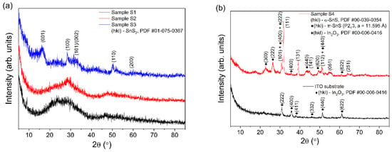
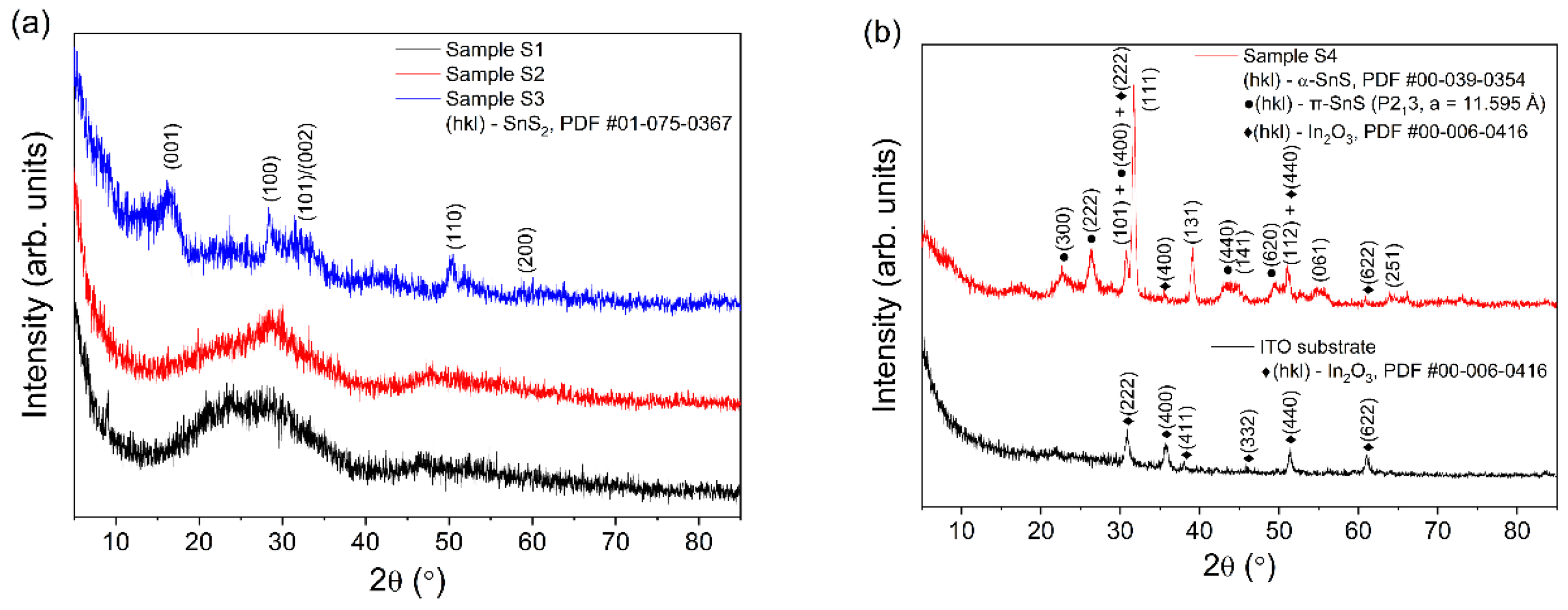
Figure 2 shows the grazing-incidence X-ray diffraction (GIXRD, Cu Kα, α = 0.3°) patterns of the films deposited on glass (Figure 2a) and on ITO/glass (Figure 2b), the latter together with the pattern of the bare ITO substrate. Phase identification is based on the PDF cards #01-075-0367 (SnS2, berndtite), #00-039-0354 (α-SnS, herzenbergite) and #00-006-0416 (In2O3, bixbyite).
Figure 2.
XRD patterns (Cu Kα, α = 0.3°) of (a) the films deposited on glass (sample S1 and sample S2—amorphous Cu–Sn–S; sample S3—SnS2) and (b) the SnS film deposited on ITO/glass (sample S4), together with the bare ITO substrate. In (a), the (hkl) indices refer to SnS2 (berndtite, PDF #01-075-0367). In (b), unmarked (hkl) indices refer to orthorhombic α-SnS (PDF #00-039-0354), filled circles (●) to cubic π-SnS (space group P213, a = 11.595 Å [48,49]), and filled diamonds (♦) to In2O3 of the ITO substrate (PDF #00-006-0416); overlapping contributions are indicated with “+”.
The Cu–Sn–S films (sample S1, Cu:Sn = 1:1 and sample S2, Cu:Sn = 2:1) showed no Bragg reflections and are therefore amorphous; any crystalline fraction is below the detection limit of the measurement. Their patterns contain only broad halos superimposed on the scattering of the glass substrate: for sample S1, two overlapping halos of comparable intensity centered at 2θ ≈ 22.3° and ≈ 28.7°, whereas for sample S2 the low-angle halo weakens and the pattern is dominated by a single halo at 2θ ≈ 28.8°, accompanied by a broad halo around 2θ ≈ 51°. Since the substrate is identical, this composition-dependent redistribution reflects a change in the average local order of the amorphous films: the halo positions of the strongly Cu-rich sample S2 (Cu/Sn ≈ 16 by XRF) are close to the strongest reflection clusters of covellite-type CuxS, while the additional halo at larger distances in sample S1 suggests a more significant Sn–S contribution.
For the SnS film deposited on the glass (sample S3), the pattern shows the reflections of hexagonal SnS2 (berndtite, space group P-3m1, PDF card #01-075-0367); no reflections of orthorhombic SnS are observed for sample S3 either. The line widths are strongly anisotropic: the in-plane (hk0) reflections, such as (100) at 2θ ≈ 28.5°, (110) at ≈ 50.3°, and (200) at ≈ 58.8°, are relatively narrow and correspond to a crystallite size of ≈ 11–13 nm, whereas the basal (001) reflection is very broad (FWHM ≈ 2.8°), corresponding to an interlayer spacing of d ≈ 5.4 Å. The maximum of the (001) reflection (2θ ≈ 16.3°, d ≈ 5.4 Å) is displaced from the reference basal spacing (5.90 Å), and the (002) and (101) reflections merge into a single broad asymmetric band at 2θ ≈ 29–34°, whose maximum was labelled (101)/(002). This pronounced size anisotropy shows that the sample S3 film consists of two-dimensional SnS2 nanoplates, in full agreement with the flake-like morphology observed by AFM (see Section 3.4).
In the diffraction pattern of the film deposited on ITO (sample S4, Figure 2b), in addition to the reflections of the cubic In2O3 (bixbyite) phase of the ITO substrate ((222), (400), (411), (332), (440), and (622); PDF #00-006-0416), the diffraction lines at 2θ ≈ 30.8, 31.7, 39.1, 44.8, and 51.1° are indexed as the (101), (111), (131), (141), and (112) reflections of orthorhombic α-SnS (herzenbergite, space group Pnma, PDF #00-039-0354), together with weaker features in the 54–56° region ((061)/(132)). The lattice parameters refined from the film reflections, a = 4.307(39) Å, b = 11.220(67) Å, and c = 4.002(19) Å, agree within 0.5% with the reference values. The mean crystallite size obtained from the Scherrer equation ((111)/(131)/(112) reflections) is ~ 18 nm, and the strong deviation of the relative intensities from the powder reference (e.g., suppression of the (021) and (040) reflections) indicates preferred orientation of the SnS crystallites. Two additional broad reflections at 2θ ≈ 22.7° and 26.4° (with weaker counterparts at ≈ 44.0° and 49.4°) cannot be indexed in the herzenbergite phase and do not match SnS2, Sn2S3, SnO2, or zinc-blende SnS. They share a common line width (FWHM ≈ 0.9°, corresponding to crystallites sizes of ~ 8–10 nm) that is distinctly larger than that of the herzenbergite reflections (0.44–0.48°, ~18 nm), revealing a second nanocrystalline population. All these features are consistently indexed on the cubic π-SnS phase (space group P213, a = 11.595 Å [48,49]; with a ≈ 11.6–11.7 Å in the present film) as the (300), (222), (440), and (620) reflections: of the two strongest π-SnS lines, (222) is directly observed, while (400) coincides with the SnS(101)/In2O3(222) composite peak at ≈ 30.8°. The coexistence of the metastable cubic phase with orthorhombic α-SnS agrees with the substrate- and condition-dependent competition between the two forms reported for chemically deposited SnS films [50]. The assignment of this minor fraction nevertheless remains tentative.
These results show that the crystalline state of the films is governed primarily by their composition—the Cu-containing films are amorphous, whereas the Cu-free tin sulfide films are crystalline—while the substrate selects the tin sulfide phase: two-dimensional SnS2 nanoplates form on glass, whereas orthorhombic α-SnS (accompanied by a minor cubic fraction) forms on ITO.
The phase selection can be explained by the chemistry at the substrate/solution interface. Under the low-temperature, solution-based conditions used here, the phase is determined at the nucleation stage by interfacial adsorption, heterogeneous nucleation kinetics, and the local chemical environment at the interface, and not by a subsequent thermally induced transformation [51]. Both SnS and SnS2 are obtained from Sn(II)/thioacetamide baths depending on the deposition conditions [52,53,54,55]. Since SnS2 contains Sn4+ whereas the precursor is Sn2+, the formation of SnS2 requires the partial oxidation of Sn(II) in the acidic bath, and the tin oxidation state retained in the solid is set by the competition at the growth front, between the incorporation of Sn2+ as SnS and its oxidation to Sn4+ followed by precipitation as SnS2. The glass surface is amorphous, SiO2-based and weakly charged at the working pH [56,57]; it adsorbs the tin complexes weakly, and growth proceeds mainly by the attachment of particles formed in the bath, where oxidation of Sn(II) has time to occur and the sulfur-rich SnS2 phase develops as layered nanoplates. The hydroxylated, conductive surface of ITO [58] adsorbs the Sn(II) complexes and sustains ion-by-ion nucleation, in which Sn2+ is incorporated directly as SnS before its oxidation; this interface-controlled growth yields the oriented α-SnS crystallites and the minor metastable π-SnS fraction, in line with the substrate-dependent phase selection reported for chemically deposited SnS [35,50,54,59,60,61].
3.2. X-Ray Fluorescence (XRF)
X-ray fluorescence (XRF) analysis was used to semi-quantitatively evaluate the elemental composition of the investigated thin films deposited on glass and ITO/glass substrates. The elemental composition, expressed in atomic percentages (at%), is summarized in Table 1. Due to the small thickness of the deposited films, the WDXRF signal also contains a contribution from the underlying glass or ITO/glass substrate. Therefore, the atomic percentages reported in Table 1 should be considered semi-quantitative and should not be regarded as the absolute composition of the deposited films. This effect is particularly important for oxygen because of the contribution from the oxide-containing substrates. For the copper–tin sulfide thin films deposited on glass substrates (S1 and S2 samples), the detected characteristic X-ray emission lines correspond to Cu (Kα at 8.04 keV, Kβ at 8.90 keV), Sn (Kα at 25.2 keV, Kβ at 28.4 keV), S (Kα at 2.31 keV), and O (Kα at 0.52 keV). Based on the semi-quantitative XRF data, the Cu/Sn atomic ratio of the Cu–Sn 1:1/glass thin film (S1) was estimated to be 1.26. In contrast, the Cu:Sn 2:1/glass thin film (S2) exhibited a pronounced Sn deficiency, leading to a significantly higher Cu/Sn atomic ratio (15.92). The observed Sn deficiency may be related to the partial precipitation of Sn-containing species in the chemical bath, thereby reducing the amount of Sn available for incorporation into the thin film [55].
Table 1.
Semi-quantitative elemental composition of the investigated thin film/substrate systems obtained by XRF analysis.
The XRF spectrum of the tin sulfide thin film (S3) revealed the characteristic emission lines of Sn (Kα at 25.2 keV, Kβ at 28.4 keV) and S (Kα at 2.31 keV). In the SnS/ITO thin film (S4), characteristic In (Kα at 24.21 keV and Kβ at 27.28 keV) emission lines originating from the ITO substrate were detected together with those of Sn, S, and O. The presence of In from the ITO substrate also confirms the substrate contribution to the XRF signal. XRF analysis confirmed the presence of Sn and S. However, the measured S/Sn atomic ratios deviated from the theoretical stoichiometric values of SnS2 and SnS for the S3 and S4 thin films, respectively, as identified by XRD analysis.
These differences should be interpreted with caution because of the substrate contribution to the XRF signal. In particular, the high oxygen contents cannot be quantitatively attributed to the deposited films. The determination of light elements such as oxygen by WDXRF also involves additional uncertainty [62], particularly in thin-film/substrate systems.
3.3. Raman Spectroscopy
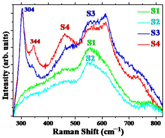
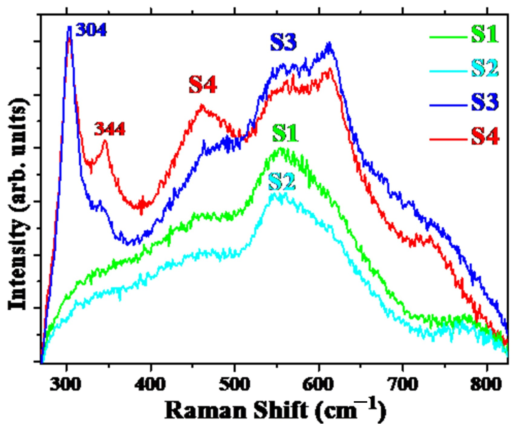
Figure 3 shows the Raman spectra of the deposited films. Samples S1 and S2 exhibit only broad asymmetric bands characteristic of amorphous materials, indicating significant structural disorder. In contrast, samples S3 and S4 display an intense Raman band at approximately 304 cm−1, attributed to Sn–S vibrational modes and consistent with the phases identified by GIXRD: hexagonal SnS2 in sample S3 and orthorhombic α-SnS in sample S4. Because of the overlap of characteristic Raman features, definitive phase identification was established by XRD analysis. A weaker band at approximately 344 cm−1 observed in S4 is attributed to the ITO substrate. Additional broad bands at ~330, 450, 550, and 620 cm−1 are tentatively assigned to disorder-related and second-order Raman scattering effects [63,64,65,66,67,68].
Figure 3.
Raman spectra of the thin films.
3.4. Atomic Force Microscopy (AFM)
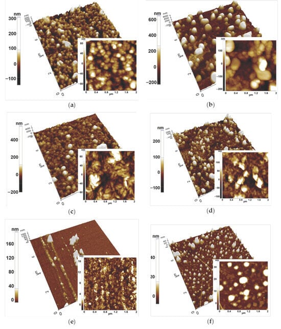
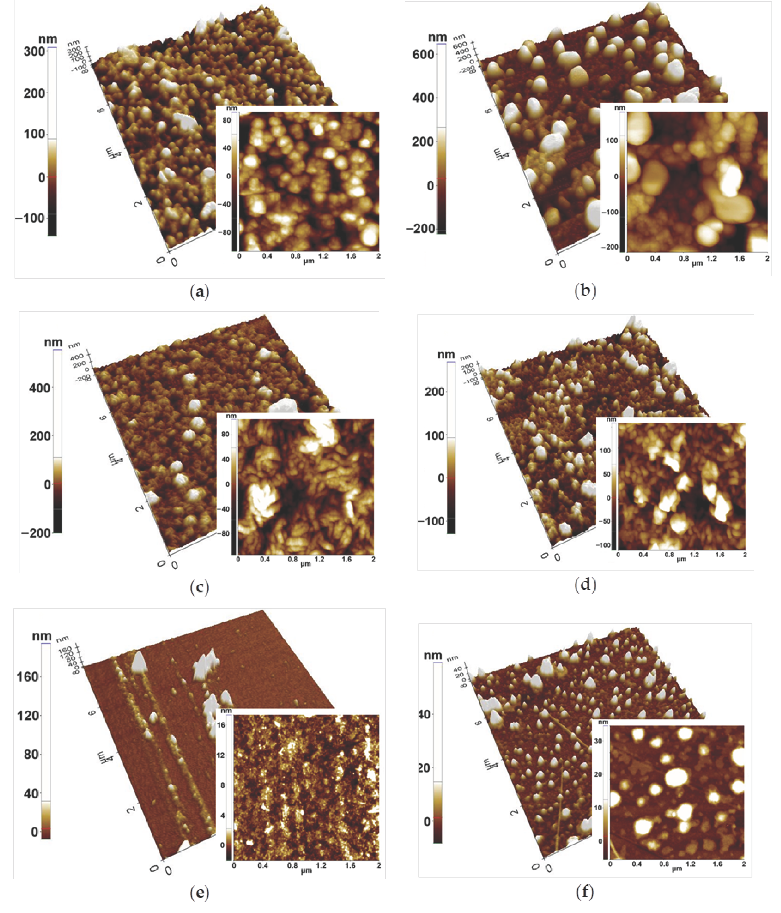
Figure 4a displays the topographic 3D AFM image of the Cu:Sn (1:1) (sample S1), at the scale of (8 μm × 8 μm), deposited on glass substrate. It can be observed that the morphology of the Cu:Sn (1:1) film consists of rounded grains (see the light spots, with diameters around 2–300 nm) with porous structure (see the dark spots). The area presented in Figure 4a is characterized by an RMS roughness of 46.0 nm. The inset presents the 3D AFM image at the scale of (2 μm × 2 μm), which suggests that each grain is composed of smaller grains of few tens of nm.
Figure 4.
3D AFM images (topography) at the scale of (8 μm × 8 μm): (a) S1—Cu:Sn (1:1)/glass; (b) S2—Cu:Sn (2:1)/glass; (c) S3—SnS2/glass; (d) S4—SnS/ITO/glass; (e) glass; (f) ITO/glass substrates. The inset images are 2D AFM images of a 2 μm × 2 μm scanned area.
By changing the Cu:Sn ratio from 1:1 to 2:1 (Figure 4b), the appearance of mostly grains (5–600 nm or even larger) distributed randomly can be observed. This causes an increase of more than two times the RMS surface roughness, up to 120.5 nm.
The SnS2 film deposited on glass (sample S3) exhibits a completely different morphology consisting of hemispherical formations with a cauliflower-like appearance (RMS roughness of 54.8 nm). The inset of Figure 4c reveals that the cauliflower-like formations are composed of flakes with a sub-structure of grains (two-dimensional SnS2 nanoplates) which can be assigned to the hexagonal SnS2, as suggested by XRD analysis.
The SnS film deposited on ITO (sample S4—Figure 4d) seems to present a less uniform morphology (RMS roughness of 47.8 nm), while the detailed image presented in the inset shows a granular structure, consistent with the prevalent orthorhombic α-SnS and the minor cubic π-SnS fraction identified by XRD [50]. Finally, the images of the glass (Figure 4e) and ITO/glass (Figure 4f) are presented, characterized by RMS roughness values of 14.9 nm (glass) and 6.8 nm (ITO/glass) at the scale of (8 μm × 8 μm).
3.5. Optical Properties
The optical properties (refractive index (n), extinction coefficient (k), band gap (Eg), and transmission (T)) of the Cu–Sn–S thin films deposited on glass were investigated using spectroscopic ellipsometry (SE). The spectra analysis was done using a General Oscillator (Lorentz) model from WVASE32™ software package [69]. The roughness film was simulated by the effective medium approximation-EMA (50% voids + 50% Cu–Sn–S film) [70].
The variation of refractive index (n) and extinction coefficient (k) with the wavelength of Cu–Sn–S, SnS thin films is represented in Figure 5a,b. The refractive index films varied in the range of 2.36–1.55, and the extinction coefficients (k) varied in the range of 1.34–0.18. The refractive index variation of the films follows a decreasing trend with increasing roughness (see AFM) [71].
The optical band-gap energy (Eg) of these films was calculated using the spectral dependence of the absorption coefficient, α, and the values derived from the ellipsometric extinction coefficient, k, (α = 4πk/λ) by constructing Tauc plots: (αhν)2 vs. photon energy (hν) for direct transitions (presented in Supplementary Material) [72]. The observed decrease of the optical band gap with the composition ratios of Cu–Sn thin film are similar to those reported by Guddeti et al. [73]. Its values are also dependent on substrate type—thickness and poor crystallinity of the films lead to a higher optical band gap [74].
The transmission spectra of the Cu–Sn–S thin films were measured by J. A Woollam VASE ellipsometer in the 250–1700 nm range, and the optical absorption coefficient (α) values of thin films were calculated from the transmittance spectra by using Equation (1) [72]:
where α is the absorption coefficient, d is the film thickness, and T is the transmittance of the thin films.
Figure 5c,d show the results of the transmission and the absorption coefficient data of the Cu–Sn–S thin films, respectively. The transmission of the S1 and S2 thin films decreased from 75 to ~60% which may be attributed to the composition ratios of Cu:Sn. At the same time it varies very much with substrate—S3 having double the value of transmission than S4.
It can be observed that the absorption coefficient reaches values as high as 104 cm−1 in the visible spectral range and infrared suggesting an allowed direct electronic transition. These values make the Cu–Sn–S thin film suitable for solar cell applications [75]. The optical results show that Cu–Sn–S thin films have an energy gap in the range of (2.24–2.70 eV) with a high coefficient of absorption, making them suitable for potential applications involving solar cells.
Figure 5.
Refractive index (a), extinction coefficient (b), optical transmission (c), and absorption coefficient (d) of S1–S4 thin films (Alias et al., 2019 - Ref. [76]).
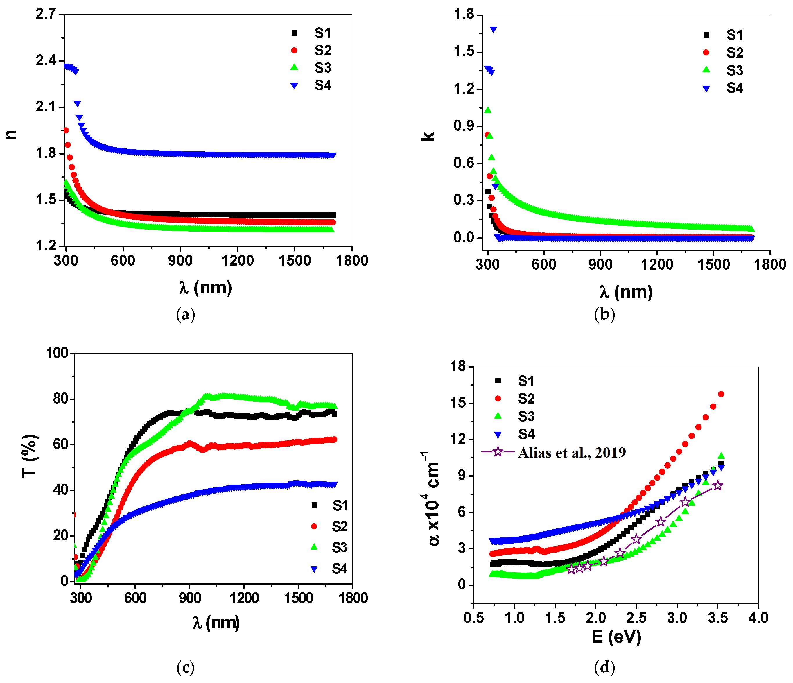
A previous study published by M.F.A. Alias et al. [76] investigated Cu–Sn–S thin films deposited on glass substrates by chemical bath deposition at temperatures ranging from 313 to 343 K. The results demonstrated that the obtained materials had suitable properties for photovoltaic applications. In the present work, we aimed to demonstrate that Cu–Sn–S films with comparable properties can also be deposited using the same chemical bath deposition method at low temperature. To facilitate this comparison, the α spectrum, reported in the previous study (of the sample with a ratio of Cu/Sn/S = 20/10/30 treated at 343 K and a thickness of 27 nm) was included alongside our experimental results. As shown, the agreement between the spectra is very good, supporting the feasibility of low-temperature deposition while achieving comparable optical properties.
Although the two synthesis methods differ in their chemical precursors and deposition conditions, both yield copper–tin sulfide thin films with comparable characteristics. The cited method uses sodium thiosulfate as the sulfur precursor and the films were obtained after 80 min at 313–343 K and varying pH, whereas our method employs thioacetamide, EDTA-Na2, and Tween 20, with deposition conducted for 4 h at 343 K. Despite these differences, the films prepared in this study exhibit a high absorption coefficient, indicating favorable light-absorption properties for potential photovoltaic and optoelectronic applications. In this sense it has been shown that an interlayer can modulate charge extraction and recombination in photovoltaic devices [77]. These results demonstrate that suitable copper–tin sulfide films can be obtained through different chemical bath or precipitation routes, although precursor chemistry and deposition parameters can affect their optical response.
The optical bandgap value for tin disulfide (SnS2), berndtite, is generally in the range of 2.1–2.6 eV for direct transitions, being considered a wide-band n-type semiconductor (~2.6 eV) in [78].
Due to the fact that the exact value depends on the sample preparation (single crystal, thin films, nanostructures) and the type of electronic transition, the Eg values reported in the literature vary as follows: (i) direct bandgap reported to be between 2.2 eV and 2.5 eV at room temperature—2.2 eV was reported in [79]; (ii) indirect bandgap—the basic structure of SnS2 often exhibits a somewhat smaller indirect bandgap, experimentally determined to be around 1.8 eV–2.34 eV [80]. The optical band gap of some chemical bath deposited SnS2 films for thin film solar cells, showed an optical energy band gap in the range of 2.95–2.80 eV [53].
Note that the influence of morphology and size was reported in nanostructured samples (quantum dots and 2D nanoflakes) due to the quantum confinement effect by increasing the optical gap towards 2.6 eV–2.7 eV [81]. On the other hand, for thin films the Eg values can vary over a wide range, from 1.8 eV to 2.9 eV in some mixed chemical phases, depending on the deposition method and thermal treatments.
Tin monosulfide in its stable phase at room temperature (orthorhombic α-SnS, herzenbergite) has a fundamental indirect optical bandgap of about 1.07–1.11 eV, closely followed by a direct bandgap of about 1.21–1.25 eV [82]. As in the case of SnS2, the exact measured value varies depending on the morphology and dimensionality. For example, for thin films obtained by various deposition methods the optical gap value tends to increase slightly due to lattice defects, internal stress storage, or stoichiometry variations, and the experimentally reported values are usually between 1.3 eV and 1.6 eV [83]. Additionally, the bandgap also increases significantly, reaching theoretical and experimental values between 1.4 eV and 1.9 eV for nanostructured materials (e.g., 2D nanoflakes) [84].
Taking into consideration all these data reported in the literature and not having available the density of the states modeled on these materials, we consistently analyzed all samples under the presumption of direct optical transitions. However, the nanostructured morphology of the samples and the phase mixture observed in the case of sample S4 make it difficult to analyze the optical properties of these samples.
The structural and optical characteristics of the S1–S4 samples are presented comparatively in Table 2, providing a comprehensive overview of the variations observed among the investigated samples. The tabulated results highlight the changes in the structural parameters and corresponding optical properties, thereby facilitating a direct comparison and enabling a clearer understanding of the influence of the sample composition or processing conditions on their overall structural, morphological, and optical behavior.
Table 2.
Structure, roughness, transmission, thickness, band gap, and absorption coefficients of S1–S4 samples.
The obtained results demonstrate that both film composition and substrate significantly influence the crystallinity, morphology, and optical response of chalcogenide thin films. In particular, the comparative analysis reveals a strong correlation between the composition control, the Cu:Sn molar ratio, the substrate-induced structural evolution, and the resulting optical characteristics, providing insights into the optimization of these materials for photovoltaic absorber layers. The combined use of complementary characterization techniques enables a comprehensive assessment of the structure–morphology–optical property relationships, which is essential for controlling the performance of chemically deposited chalcogenide films. These findings underscore the potential of copper–tin sulfide and tin sulfide thin films as tunable absorber materials and provide valuable insights for their effective integration into hybrid solar-cell architectures.
Electrical properties were not evaluated in this work. The phases identified by GIXRD nevertheless determine the expected conductivity type: SnS2 is an n-type semiconductor, whereas α-SnS and π-SnS are p-type, with carrier concentrations of 1015–1018 cm−3 and resistivities of 101–104 Ω cm reported for chemically deposited films [52,85,86]. The substrate-dependent phase selection thus implies a change of conductivity type, from n-type SnS2 on glass to p-type SnS on ITO/glass.
4. Conclusions
Copper–tin sulfide and tin sulfide thin films were successfully prepared by chemical bath deposition at low temperature on glass and ITO/glass substrates, proving the suitability of this low-cost and scalable technique for preparing chalcogenide absorber layers for potential photovoltaic applications.
The experimental results indicate that both the film composition and the substrate nature strongly influence the structural, morphological, and optical characteristics of the deposited layers. XRD analysis revealed that Cu–Sn–S films deposited on glass are predominantly amorphous, while SnS films grown on ITO/glass exhibit a crystalline orthorhombic structure, revealing the important role of the substrate in promoting crystallization. On the relatively inert SiO2 surface, the slower nucleation process may favor the oxidation of Sn(II) to Sn(IV) and subsequent formation of sulfur-rich SnS2. In contrast, the chemically active and electrically conducting ITO surface can promote preferential adsorption and heterogeneous nucleation of Sn(II), favoring direct reaction with sulfur-containing species generated from thioacetamide and formation of SnS.
AFM investigations showed significant variations in surface morphology with composition. The Cu:Sn (2:1) film exhibited the highest surface roughness (120.5 nm) and larger grain sizes, whereas the Cu:Sn (1:1) film presented a more homogeneous granular morphology. SnS films displayed characteristic cauliflower-like and granular structures depending on the used substrate.
Optical measurement results showed high absorption coefficients in the visible spectral range, reaching values close to 4 × 104 cm−1, which are favorable for potential photovoltaic applications. Among the investigated samples, the Cu:Sn (1:1) film exhibited the highest optical transmission at 630 nm (64.9%), while the Cu:Sn (2:1) layer showed the largest absorption coefficient and the lowest optical band gap (2.24 eV). Raman spectroscopy confirmed the presence of Sn–S vibrational modes and copper sulfide-related phases.
In conclusion, the results suggest that controlling the composition together with an appropriate choice of substrate provides an effective route for tailoring the structural and optical properties of chalcogenide thin films. These materials show promising characteristics for their integration as absorber or interfacial layers in hybrid solar cell architectures.
Supplementary Materials
The following supporting information can be downloaded at https://www.mdpi.com/article/10.3390/pr14203323/s1, Figure S1: The corresponding direct transition Tauc plots of the samples S1–S4.; Table S1—Eg values obtained from the linear fit analysis.
Author Contributions
Conceptualization, M.G. (Mariuca Gartner), E.R., M.G. (Maxim Ganchev), and V.P.; methodology, M.G. (Mariuca Gartner), M.A., J.M.C.M., S.P., I.A., H.S., M.N., E.R., M.G. (Maxim Ganchev), V.P., S.S.; S.T.; software, M.G. (Mariuca Gartner), M.C., D.M.; validation M.G. (Mariuca Gartner), M.A., J.M.C.M., S.P., I.A., H.S., M.N., M.C., D.M., E.R., M.G. (Maxim Ganchev), V.P., S.S., and S.T.; formal analysis, M.G.(Mariuca Gartner), M.A., J.M.C.M., S.P., I.A., M.N., S.S. and S.T.; investigation, M.G. (Mariuca Gartner), M.A., J.M.C.M., S.P., I.A., M.N., H.S., S.S., and S.T.; resources, M.G. (Mariuca Gartner), M.C., H.S., D.M.; M.G. (Maxim Ganchev),V.P.; data curation, M.G. (Mariuca Gartner), M.A., J.M.C.M., S.P., I.A., M.N.; writing—original draft preparation, M.G. (Mariuca Gartner), M.A., J.M.C.M., S.P., I.A., M.C., E.R., M.G. (Maxim Ganchev), V.P.; writing—review and editing, M.G. (Mariuca Gartner), H.S., and M.C.; visualization, M.G. (Mariuca Gartner); supervision, M.G. (Mariuca Gartner); project administration, M.G. (Mariuca Gartner). All authors have read and agreed to the published version of the manuscript.
Funding
This work is partially supported by the Bulgarian National Science Fund contracts KP06-H77/14.12.2023 and KP06 COST/16/14.12.2023, EU COST Action 21148 ReNewPV, and NSI ESHER, funded by the Bulgarian Ministry of Science and Education.
Data Availability Statement
The original contributions presented in this study are included in the Article/Supplementary Material. Further inquiries can be directed to the corresponding authors.
Acknowledgments
This paper was carried out within the research program “Science of Surfaces and Thin Layers” of the Ilie Murgulescu Institute of Physical Chemistry financed by the Romanian Academy. All authors acknowledge the support of the Collaboration Agreement between the Romanian and Bulgarian Academies of Science.
Conflicts of Interest
The authors declare no conflicts of interest.
References
- Holechek, J.L.; Geli, H.M.E.; Sawalhah, M.N.; Valdez, R. A Global Assessment: Can Renewable Energy Replace Fossil Fuels by 2050? Sustainability 2022, 14, 4792. [Google Scholar] [CrossRef] [Scilit]
- Thomas, P.; Collins, A.R. The impacts of development on energy transition. Renew. Energy 2026, 271, 125871. [Google Scholar] [CrossRef] [Scilit]
- Glavina, A.; Mišić, K.; Baleta, J.; Wang, J.; Mikulčić, H. Economic development and climate change: Achieving a sustainable balance. Clean. Eng. Technol. 2025, 26, 100939. [Google Scholar] [CrossRef] [Scilit]
- Sompolska-Rzechuła, A.; Bąk, I.; Becker, A.; Marjak, H.; Perzyńska, J. The Use of Renewable Energy Sources and Environmental Degradation in EU Countries. Sustainability 2024, 16, 10416. [Google Scholar] [CrossRef] [Scilit]
- Afuye, G.A.; Tolios, G. Quantitative impacts and patterns of greenhouse gas emission trends: Implications for global change and policy. Carbon Manag. 2026, 17, 2622340. [Google Scholar] [CrossRef] [Scilit]
- Islam, S.; Ghosh, S.; Su, W. Transition from Fossil Fuels to Renewables: A Comparative Analysis Between Energy-Rich and Energy-Poor Economies. Commodities 2026, 5, 9. [Google Scholar] [CrossRef] [Scilit]
- Guo, J.; Chen, C.; Dong, X.; Li, X.; Zhao, Q.; Zhang, M.; Yang, C. Multi-functional liquid metal/carbon nanotubes/bacterial cellulose flexible composite film, suitable for electromagnetic shielding, intelligent wearable sensors and joule heater materials. Colloids Surf. A Physicochem. Eng. Asp. 2026, 752, 141829. [Google Scholar] [CrossRef] [Scilit]
- Li, C.; Liu, P.; Zhao, M.; Zhang, Y.; Bao, H.; Yang, M.; Chen, Y.; Zhong, G. Regulation mechanism of dielectric constant on ion transport behavior in vinylidene fluoride-based solid composite electrolytes. Electrochim. Acta 2026, 573, 149499. [Google Scholar] [CrossRef] [Scilit]
- Sharma, V.K.; Monteleone, G.; Braccio, G.; Anyanwu, C.N.; Aneke, N.N. A Comprehensive Review of Green Energy Technologies: Towards Sustainable Clean Energy Transition and Global Net-Zero Carbon Emissions. Processes 2024, 13, 69. [Google Scholar] [CrossRef] [Scilit]
- Formolli, M.; Kleiven, T.; Lobaccaro, G. Assessing solar energy accessibility at high latitudes: A systematic review of urban spatial domains, metrics, and parameters. Renew. Sustain. Energy Rev. 2023, 177, 113231. [Google Scholar] [CrossRef] [Scilit]
- Järvinen, M.; Paulomäki, H.; Oksanen, E.; Khatiwada, D.; El Geneidy, S.; Peura, M.; Kotiaho, J.S.; Herzon, I.; Apajalahti, E.-L.; Dańkowska, A.; et al. A Sustainable Path for Renewable Energy Technologies. In Designing Renewable Energy Systems within Planetary Boundaries. Green Energy and Technology; Järvinen, M., Paulomäki, H., Eds.; Springer: Cham; Switzerland, 2025; pp. 33–127. [Google Scholar] [CrossRef] [Scilit]
- Maka, A.O.M.; Ghalut, T.; Elsaye, E. The pathway towards decarbonisation and net-zero emissions by 2050: The role of solar energy technology. Green Technol. Sustain. 2024, 2, 100107. [Google Scholar] [CrossRef] [Scilit]
- Lazaroiu, A.C.; Gmal Osman, M.; Strejoiu, C.-V.; Lazaroiu, G. A Comprehensive Overview of Photovoltaic Technologies and Their Efficiency for Climate Neutrality. Sustainability 2023, 15, 16297. [Google Scholar] [CrossRef] [Scilit]
- Priya, P.; Stonier, A.A. Emerging innovations in solar photovoltaic (PV) technologies: The perovskite solar cells and more. Energy Rep. 2025, 14, 216–242. [Google Scholar] [CrossRef] [Scilit]
- Areola, R.I.; Adebiyi, A.A.; Reddy, D.J. From Optimization to Investment: A Techno-Economic Assessment of NSGA-II Optimized Grid-Connected Photovoltaic–Energy Storage Systems in Developing Economies. Solar 2026, 6, 31. [Google Scholar] [CrossRef] [Scilit]
- Prakash, K.; Ahmed, I.; Mobin, S.M. Strategic development of stable and efficient lead-free perovskite solar cells. Commun. Mater. 2026, 7, 144. [Google Scholar] [CrossRef] [Scilit]
- Di Sabatino, M.; Hendawi, R.; Garcia, A.S. Silicon Solar Cells: Trends, Manufacturing Challenges, and AI Perspectives. Crystals 2024, 14, 167. [Google Scholar] [CrossRef] [Scilit]
- Machín, A.; Márquez, F. Advancements in Photovoltaic Cell Materials: Silicon, Organic, and Perovskite Solar Cells. Materials 2024, 17, 1165. [Google Scholar] [CrossRef] [Scilit] [PubMed]
- Seyisi, T.; Fouda-Mbanga, B.G.; Mnyango, J.I.; Nthwane, Y.B.; Nyoni, B.; Mhlanga, S.; Hlangothi, S.P.; Tywabi-Ngeva, Z. Major challenges for commercialization of perovskite solar cells: A critical review. Energy Rep. 2025, 13, 1400–1415. [Google Scholar] [CrossRef] [Scilit]
- Berg, D.M.; Djemour, R.; Gütay, L.; Zoppi, G.; Siebentritt, S.; Dale, P.J. Thin film solar cells based on the ternary compound Cu2SnS3. Thin Solid Films 2012, 520, 6291–6294. [Google Scholar] [CrossRef] [Scilit]
- Intal, D.; Ebong, A.U. Thin-film solar photovoltaics: Trends and future directions. Renew. Sustain. Energy Rev. 2026, 226, 116464. [Google Scholar] [CrossRef] [Scilit]
- Njema, G.G.; Kibet, J.K. A review of chalcogenide-based perovskites as the next novel materials: Solar cell and optoelectronic applications, catalysis and future perspectives. Next Nanotechnol. 2025, 7, 100102. [Google Scholar] [CrossRef] [Scilit]
- Alfred, M.O.; Akor, E.; Ayeni, B.C.; Olorunnisola, C.G.; Unuabonah, E.I.; Omorogie, M.O. Chalcogenides: Recent advances in their environmental applications. Energ. Ecol. Environ. 2026, 11, 10–38. [Google Scholar] [CrossRef] [Scilit]
- Sivasamy, R.; Kaliyan, G.; Kaliyamoorthy, S.; Mosquera, E. Chalcogenide Materials for Sustainable Energy and Environmental Applications. In Structural and Chemical Features of Chalcogenides; IntechOpen: London, UK, 2024. [Google Scholar] [CrossRef] [Scilit]
- Menon, K.G.; Venugopalan, A.T.; Punathil, P.; Zoppi, G.; Vijayan, V.T. Chalcogen Incorporation in Cu−Sn−S Absorbers: Structural, Optical, and Photovoltaic Performance of Simulation-Guided CTS and CTSSe Solar Cells. ACS Appl. Energy Mater. 2026, 9, 8311–8323. [Google Scholar] [CrossRef] [Scilit]
- Soonmin, H.; Paulraj, I.; Kumar, M.K.; Sonker, R.; Nandi, P. Recent Developments on the Properties of Chalcogenide Thin Films. In Chalcogenides—Preparation and Applications; IntechOpen: London, UK, 2022. [Google Scholar] [CrossRef] [Scilit]
- Koskela, K.M.; Mora Perez, C.; Eremin, D.B.; Evans, J.M.; Strumolo, M.J.; Lewis, N.S.; Prezhdo, O.V.; Brutchey, R.L. Polymorphic Control of Solution-Processed Cu2SnS3 Films with Thiol-Amine Ink Formulation. Chem. Mater. 2022, 34, 8654–8663. [Google Scholar] [CrossRef] [Scilit] [PubMed]
- Erkan, S.; Atasoy, Y.; Olgar, M.A.; Zan, R. Influence of solvent chemistry and pre-annealing temperature on the structural optical and electrical properties of solution-processed CTS thin films. J. Mater. Sci. Mater. Electron. 2026, 37, 754. [Google Scholar] [CrossRef] [Scilit]
- Ibrahim, N.M.; Mahdi, M.S.; Abdullah, M.M.; Muhammad, K.A. Influence of growth temperature on the structural and optoelectronic properties of SnS thin films deposited by chemical bath deposition on flexible substrates. Appl. Phys. A 2026, 132, 780. [Google Scholar] [CrossRef] [Scilit]
- Porcar-Garcia, S.; Lahlahi, A.; Toca, S.; T. Papanastasiou, D.; Cuadra, J.G.; Muñoz-Roja, D.; Carda, J.B. Non-Conventional Substrates for Photovoltaic Technologies: Materials, Interfaces and Processing Constraints. Solar 2026, 6, 28. [Google Scholar] [CrossRef] [Scilit]
- Priyadarshini, P.; Das, S.; Naik, R. A review on metal-doped chalcogenide films and their effect on various optoelectronic properties for different applications. RSC Adv. 2022, 12, 9599–9620. [Google Scholar] [CrossRef] [Scilit] [PubMed]
- Safrani, T.; Jopp, J.; Golan, Y. A comparative study of the structure and optical properties of copper sulfide thin films chemically deposited on various substrates. RSC Adv. 2013, 3, 23066–23074. [Google Scholar] [CrossRef] [Scilit]
- Zaki, M.Y.; Sava, F.; Simandan, I.D.; Buruiana, A.T.; Mihai, C.; Velea, A.; Galca, A.C. Effect of the stacking order, annealing temperature and atmosphere on crystal phase and optical properties of Cu2SnS3. Sci. Rep. 2022, 12, 7958. [Google Scholar] [CrossRef] [Scilit] [PubMed]
- Vinita, C.K.; Yadav, R.P.; Singh, B.K. Thickness-dependent surface morphology, fractality, and its influence on the opto-electrical performance of SnS thin films for photodetector applications. Emergent Mater. 2025, 8, 5273–5302. [Google Scholar] [CrossRef] [Scilit]
- Ayala-Mató, F.; López-Cruz, L.A.; Barrios-Salgado, E.; Nair, M.T.S.; Nair, P.K. Chemically deposited cubic/orthorhombic SnS superstrate solar cells with ZnS-CdS window and copper selenide back interface layers. J. Alloys Comp. 2026, 1053, 186107. [Google Scholar] [CrossRef] [Scilit]
- Yongke, L.; Xu, J.; Guo, H.; Li, B.; Shi, Z. Emerging Perovskite Solar Cells for Building-Integrated Photovoltaic Applications. IFM 2026, 3, 156–177. [Google Scholar] [CrossRef] [Scilit]
- Frach, P.; Glöß, D.; Goedicke, K.; Fahland, M.; Gnehr, W.-M. High rate deposition of insulating TiO2 and conducting ITO films for optical and display applications. Thin Solid Films 2003, 445, 251–258. [Google Scholar] [CrossRef] [Scilit]
- Ali, K.; Khan, S.A.; Jafri, M.Z.M. Structural and optical properties of ITO/TiO2 anti-reflective films for solar cell applications. Nanoscale Res. Lett. 2014, 9, 175. [Google Scholar] [CrossRef] [Scilit] [PubMed]
- Ge, S.; Sang, D.; Zou, L.; Yao, Y.; Zhou, C.; Fu, H.; Xi, H.; Fan, J.; Meng, L.; Wang, C. A Review on the Progress of Optoelectronic Devices Based on TiO2 Thin Films and Nanomaterials. Nanomaterials 2023, 13, 1141. [Google Scholar] [CrossRef] [Scilit] [PubMed]
- Li, J.; Jiang, L.; Li, X.; Luo, J.; Liu, J.; Wang, M.; Yan, Y. Different Crystallization Behavior of Amorphous ITO Film by Rapid Infrared Annealing and Conventional Furnace Annealing Technology. Materials 2023, 16, 3803. [Google Scholar] [CrossRef] [Scilit] [PubMed]
- Raaif, M.; El-Hossary, F.M.; El-Moula, A.A.A.; Abo El-Kassem, M. A comparative study of the optical, electrical, and wettability properties of amorphous and nanocrystalline ITO/Cu/ITO multilayer thin films prepared by DC pulsed magnetron sputtering. Appl. Phys. A 2025, 131, 603. [Google Scholar] [CrossRef] [Scilit]
- Marcelis, E.J.; ten Elshof, J.E.; Morales-Masis, M. Titanium Dioxide: A Versatile Earth-Abundant Optical Material for Photovoltaics. Adv. Opt. Mater. 2024, 12, 2401423. [Google Scholar] [CrossRef] [Scilit]
- Pereira, J.; Souza, R.; Moita, A. Engineering of Optoelectronic Devices for Renewable Energy Applications. Micromachines 2026, 17, 758. [Google Scholar] [CrossRef] [Scilit] [PubMed]
- Fekadu, G.H.; Tizazu, A. Short Review of Factors Affecting Chemical Bath Deposition Method for Metal Chalcogenide Thin Films. Int. J. Thin Fil. Sci. Tec. 2019, 8, 43–53. Available online: https://www.naturalspublishing.com/files/published/191866y1ppc9no.pdf (accessed on 14 August 2026). [CrossRef] [PubMed]
- Salem, K.H.; Mohammed, K.A.; Shumaran, D.A.; Algburi, S.; Alkhafaji, M.A.; Zabibah, R.S.; Alsultany, F.H.; Sharma, S.; Kozak, D.; Abbas, M.; et al. Deposition of Fe-CdZnS doped chalcogenide based thin films employing chemical bath deposition method: Studies on microstructural morphology, optical, and electrical, properties for photovoltaic applications. Appl. Phys. A 2024, 130, 549. [Google Scholar] [CrossRef] [Scilit]
- Sengupta, S.; Aggarwal, R.; Raula, M. A review on chemical bath deposition of metal chalcogenide thin films for heterojunction solar cells. J. Mat. Res. 2023, 38, 142–153. [Google Scholar] [CrossRef] [Scilit]
- Soonmin, H.; Sunny, G.; Vanalakar, S.A. Studies on Cu2SnS3 thin films: Review. J. Eng. Appl. Sci. 2018, 13, 4152–4159. [Google Scholar]
- Rabkin, A.; Samuha, S.; Abutbul, R.E.; Ezersky, V.; Meshi, L.; Golan, Y. New Nanocrystalline Materials: A Previously Unknown Simple Cubic Phase in the SnS Binary System. Nano Lett. 2015, 15, 2174–2180. [Google Scholar] [CrossRef] [Scilit] [PubMed]
- Abutbul, R.E.; Garcia-Angelmo, A.R.; Burshtein, Z.; Nair, M.T.S.; Nair, P.K.; Golan, Y. Crystal structure of a large cubic tin monosulfide polymorph: An unraveled puzzle. CrystEngComm 2016, 18, 5188–5194. [Google Scholar] [CrossRef] [Scilit]
- Márquez, I.G.; Romano-Trujillo, R.; Gracia-Jiménez, J.M.; Galeazzi, R.; Silva-González, N.R.; García, G.; Coyopol, A.; Nie-to-Caballero, F.G.; Rosendo, E.; Morales, C. Cubic, orthorhombic and amorphous SnS thin films on flexible plastic substrates by CBD. J. Mater. Sci. Mater. Electron. 2021, 32, 15898–15906. [Google Scholar] [CrossRef] [Scilit]
- Rudzinski, W.; Plazinski, W. Theoretical description of the kinetics of solute adsorption at heterogeneous solid/solution interfaces. Appl. Surf. Sci. 2007, 253, 5827–5840. [Google Scholar] [CrossRef] [Scilit]
- Gedi, S.; Minnam Reddy, V.R.; Kotte, T.R.R.; Park, C.; Kim, W.K. Fundamental Aspects and Comprehensive Review on Physical Properties of Chemically Grown Tin-Based Binary Sulfides. Nanomaterials 2021, 11, 1955. [Google Scholar] [CrossRef] [Scilit] [PubMed]
- Gedi, S.; Minnam Reddy, V.R.; Pejjai, B.; Park, C.; Jeon, C.-W.; Kotte, T.R.R. Studies on chemical bath deposited SnS2 films for Cd-free thin film solar cells. Ceram. Int. 2017, 43, 3713–3719. [Google Scholar] [CrossRef] [Scilit]
- Chalapathi, U.; Poornaprakash, B.; Park, S.-H. Chemically deposited cubic SnS thin films for solar cell applications. Sol. Energy 2016, 139, 238–248. [Google Scholar] [CrossRef] [Scilit]
- Mnari, M.; Kamoun, N.; Bonnet; Dachraoui, J.M. Chemical Bath Deposition of tin sulphide thin films in acid solution. Comptes Rendus Chim. 2009, 12, 824–827. [Google Scholar] [CrossRef] [Scilit]
- Comas-Vives, A. Amorphous SiO2 surface models: Energetics of the dehydroxylation process, strain, ab initio atomistic thermodynamics and IR spectroscopic signatures. Phys. Chem. Chem. Phys. 2016, 18, 7475–7482. [Google Scholar] [CrossRef] [Scilit] [PubMed]
- Kosmulski, M. Isoelectric points and points of zero charge of metal (hydr)oxides: 50 years after Parks’ review. Adv. Colloid Interface Sci. 2016, 238, 1–61. [Google Scholar] [CrossRef] [Scilit] [PubMed]
- Harrell, J.; Acikgoz, M.; Lieber Sasson, H.; Visoly-Fisher, I.; Genova, A.; Pavanello, M. Models of Surface Morphology and Electronic Structure of Indium Oxide and Indium Tin Oxide for Several Surface Hydroxylation Levels. J. Phys. Chem. C 2018, 122, 584–595. [Google Scholar] [CrossRef] [Scilit]
- Aparna, N.; Philip, R.S.; Mathew, M. Deposition of SnS thin films on various substrates at room temperature. Appl. Surf. Sci. Adv. 2023, 18, 100510. [Google Scholar] [CrossRef] [Scilit]
- Sall, T.; Mollar, M.; Marí, B. Substrate influences on the properties of SnS thin films deposited by chemical spray pyrolysis technique for photovoltaic applications. J. Mater. Sci. 2016, 51, 7607–7613. [Google Scholar] [CrossRef] [Scilit]
- Sazideh, M.R.; Ehsani, M.H.; Shahidi, M.M.; Rezagholipour Dizaji, H. Growth mechanism of nano-plates structured SnS films on different substrates in glancing angle deposition method. Sci. Rep. 2022, 12, 17913. [Google Scholar] [CrossRef] [Scilit] [PubMed]
- Breuckmann, M.; Wacker, G.; Hanning, S.; Otto, M.; Kreyenschmidt, M. Quantification of C, H, N and O in polymers using WDXRF scattering spectra and PLS regression depending on the spectral resolution. J. Anal. At. Spectrom. 2022, 37, 861–869. [Google Scholar] [CrossRef] [Scilit]
- Gartner, M.; Szekeres, A.; Simeonov, S.; Covei, M.; Anastasescu, M.; Preda, S.; Calderon-Moreno, J.M.; Predoana, L.; Stroescu, H.; Mitrea, D.; et al. Structure, Optical and Electrical Properties of Nb(Zn) Doped Sol–Gel ITO Films: Effect of Substrates and Dopants. Molecules 2024, 29, 5480. [Google Scholar] [CrossRef] [Scilit] [PubMed]
- Gawai, U.P.; Gaikwad, D.K.; Patil, S.L.; Pandey, K.K.; Lalla, N.P.; Dole, B.N. Synthesis, local structure and optical property studies of α-SnS microrods by synchrotron X-ray pair distribution function and micro-Raman shift. RSC Adv. 2020, 10, 21277–21282. [Google Scholar] [CrossRef] [Scilit] [PubMed]
- Wang, C.; Tang, K.; Yang, Q.; Qian, Y. Raman scattering, far infrared spectrum and photoluminescence of SnS2 nanocrystallites. Chem. Phys. Lett. 2002, 357, 371–375. [Google Scholar] [CrossRef] [Scilit]
- Kwon, S.H.; Kim, B.H.; Kim, D.W.; Yoon, H.; Yoon, Y.J. Vastly enhanced photoresponsivities of phase-controlled tin sulfide thin films. Nanotechnology 2020, 31, 375702. [Google Scholar] [CrossRef] [Scilit] [PubMed]
- Sofi, A.H.; Shah, M.A.; Asokan, K. Structural, Optical and Electrical Properties of ITO Thin Films. J. Electron. Mater. 2018, 47, 1344–1352. [Google Scholar] [CrossRef] [Scilit]
- Berengue, O.M.; Rodrigues, A.D.; Dalmaschio, C.J.; Lanfredi, A.J.C.; Leite, E.R.; Chiquito, A.J. Structural characterization of indium oxide nanostructures: A Raman analysis. J. Phys. D. Appl. Phys. 2010, 43, 045401. [Google Scholar] [CrossRef] [Scilit]
- Tompkins, H.G. WVASE32 Software Training Manual; J.A. Woollam Co., Inc.: Lincoln, NE, USA, 2006. [Google Scholar]
- Bruggeman, D.A.G. Berechnung verschiedener physikalischer Konstanten von heterogenen Substanzen. III. Die elastischen Konstanten der quasiisotropen Mischkörper aus isotropen Substanzen. Ann. Phys. 1937, 421, 160–178. [Google Scholar] [CrossRef] [Scilit]
- Jakhar, A.; Jamdagni, A.; Bakshi, A.; Verma, T.; Shukla, V.; Jain, P.; Sinha, N.; Arun, P. Refractive index of SnS thin nano-crystalline films. Solid State Commun. 2013, 168, 31–35. [Google Scholar] [CrossRef] [Scilit]
- Tauc, J.; Grigorovici, R.; Vancu, A. Optical Properties and Electronic Structure of Amorphous germanium. Phys. Status Solidi B 1966, 15, 627–637. [Google Scholar] [CrossRef] [Scilit]
- Guddeti, P.R.; Devi, P.M.B.; Reddy, K.R. Optical and electrical investigations on Cu2SnS3 layers prepared by two-stage process. Chin. J. Phys. 2020, 67, 458–472. [Google Scholar] [CrossRef] [Scilit]
- Hasan, B.A.; Shallal, I.H. Structural and optical properties of SnS thin films. J. Nano. Adv. Mat. 2014, 2, 43–49. [Google Scholar] [CrossRef] [Scilit]
- Cifuentes, C.; Botero, M.; Romero, E.; Calderón, C.; Gordillo, G. Optical and structural studies on SnS films grown by co-evaporation. Braz. J. Phys. 2006, 36, 1046–1049. [Google Scholar] [CrossRef] [Scilit]
- Alias, M.F.A.; Taher, B.Y.; Naji, I.S.; Iqbal, S.; Kayani, A.; Mabrook, M.F.; Al-Douri, A.A.J. Effect of Deposition Parameters on the Compositional and Optical Properties Of Cu2SnS3 Thin Films Prepared By Chemical Bath Deposition. Chalcogenide Lett. 2019, 16, 577. [Google Scholar] [CrossRef]
- Podapangi, S.K.; Mancini, L.; Takhellambam, D.; Xu, J.; Castriotta, L.A.; Mattioli, G.; Raglione, V.; Palmeri, F.; Caschera, D.; Sobolev, A.P.; et al. Improved Perovskite Solar Cells with an Environmentally Friendly Phthalocyanine Hole Extracting Interlayer. ACS Appl. Energy Mater. 2026, 9, 2541–2554. [Google Scholar] [CrossRef] [Scilit] [PubMed]
- Chakraborty, N.; Das, B.; Roy, A.; Dey, P.; Das, B.; Chattopadhyay, K.K. Wide-Bandgap 2D SnS2 -Based All-Optical Photonic Devices with Strong Nonlinear Optical Response due to Spatial Self-Phase Modulation. ACS Appl. Opt. Mater. 2024, 2, 1454–1465. [Google Scholar] [CrossRef] [Scilit]
- Ullah, S.; Bouich, A.; Ullah, H.; Mari, B.; Mollar, M. Comparative study of binary cadmium sulfide (CdS) and tin disulfide (SnS2) thin buffer layers. Sol. Energy 2020, 208, 637–642. [Google Scholar] [CrossRef] [Scilit]
- Avellaneda, D.; Sánchez-Orozco, I.; Martínez, J.A.A.; Shaji, S.; Krishnan, B. Thin films of tin sulfides: Structure, composition and optoelectronic properties. Mater. Res. Express 2018, 6, 016409. [Google Scholar] [CrossRef] [Scilit]
- Matyszczak, G.; Krawczyk, K.; Yedzikhanau, A.; Jastrzębski, C.; Dłużewski, P.; Fidler, A.; Płociński, T.; Lawniczak-Jablonska, K.; Wolska, A.; Drzewiecka-Antosik, A. Ultrasound-Assisted Synthesis of SnS2 Quantum Dots Using Acetone as Solvent. Materials 2024, 18, 82. [Google Scholar] [CrossRef] [Scilit] [PubMed]
- Banai, R.E.; Burton, L.A.; Choi, S.G.; Hofherr, F.; Sorgenfrei, T.; Walsh, A.; To, B.; Cröll, A.; Brownson, J.R.S. Ellipsometric characterization and density-functional theory analysis of anisotropic optical properties of single-crystal α-SnS. J. Appl. Phys. 2014, 116, 013511. [Google Scholar] [CrossRef] [Scilit]
- Huang, P.-C.; Huang, J.-L.; Wang, S.-C.; Shaikh, M.O.; Lin, C.-Y. Photoelectrochemical properties of orthorhombic and metastable phase SnS nanocrystals synthesized by a facile colloidal method. Thin Solid Films 2015, 596, 135–139. [Google Scholar] [CrossRef] [Scilit]
- Zhang, Y.; Shang, B.; Li, L.; Lei, J. Coupling effects of strain on structural transformation and bandgap engineering in SnS monolayer. RSC Adv. 2017, 7, 30327–30333. [Google Scholar] [CrossRef] [Scilit]
- Vidal, J.; Lany, S.; D’Avezac, M.; Zunger, A.; Zakutayev, A.; Francis, J.; Tate, J. Band-structure, optical properties, and defect physics of the photovoltaic semiconductor SnS. Appl. Phys. Lett. 2012, 100, 032104. [Google Scholar] [CrossRef] [Scilit]
- Burton, L.A.; Whittles, T.J.; Hesp, D.; Linhart, W.M.; Skelton, J.M.; Hou, B.; Webster, R.F.; O’Dowd, G.; Reece, C.; Cherns, D.; et al. Electronic and optical properties of single crystal SnS2: An earth-abundant disulfide photocatalyst. J. Mater. Chem. A 2016, 4, 1312–1318. [Google Scholar] [CrossRef] [Scilit]



Disclaimer/Publisher’s Note: The statements, opinions and data contained in all publications are solely those of the individual author(s) and contributor(s) and not of MDPI and/or the editor(s). MDPI and/or the editor(s) disclaim responsibility for any injury to people or property resulting from any ideas, methods, instructions or products referred to in the content. |
© 2026 by the authors. Licensee MDPI, Basel, Switzerland. This article is an open access article distributed under the terms and conditions of the Creative Commons Attribution (CC BY) license.