


Abstract
The strategic integration of the tunable band gap and high carrier mobility of MoS2 with the exceptional electrical conductivity of graphene offers a compelling route to circumvent the intrinsic sensing limitations of each material in isolation. Within the resulting van der Waals heterostructures, synergistic interlayer electronic coupling substantially reshapes the optoelectronic response. In particular, the MoS2/graphene interface exhibits an ultraviolet absorption coefficient of approximately 3.5 × 105 cm−1 at 350 nm, an enhancement of about 20% relative to pristine MoS2. First-principles density functional theory (DFT) calculations further show that tuning the interlayer spacing induces a finite band gap in graphene, attaining 67.8 meV at a compressed separation of 2.3 Å. Building on these electronic insights, the gas-sensing performance of the MoS2/graphene heterostructure was evaluated toward CO, CO2, NO, and HF gases. The adsorption energies, supported by electronegativity analysis, were consistently negative for oxidizing (CO2, NO), reducing (CO), and corrosive (HF) molecules, namely −70 meV, −51 meV, −363 meV, and −127 meV for CO, CO2, NO, and HF, respectively, a trend corroborated by electronegativity analysis. This energetically favorable adsorption underscores the strong gas–surface interactions enabled by the heterointerface, revealing a superior sensing response compared to either MoS2 or graphene alone. These results highlight the promising potential of MoS2/graphene heterostructures for next-generation, high-sensitivity gas-monitoring technologies.
1. Introduction
Graphene, one of the most influential scientific discoveries of the twenty-first century, is a single atomic layer of sp2-hybridized carbon atoms arranged in a hexagonal lattice and stabilized by sp2 hybridization. Since its isolation [1], its exceptional physicochemical properties have attracted intense research interest. These include an ultrahigh theoretical specific surface area (~2630 m2·g−1) [2,3], outstanding mechanical strength [4,5,6,7,8], high optical transparency from the visible to the infrared [9], and exceptionally high carrier mobility (~200,000 cm2·V−1·s−1) [10,11,12,13]. Despite these advantages, the absence of an intrinsic band gap hinders the integration of graphene into electronic and photonic devices. This challenge has motivated the exploration of alternative two-dimensional (2D) semiconductors and the engineering of van der Waals heterostructures that combine graphene with other layered materials offering controllable electronic structure. Among these, molybdenum disulfide (MoS2) and related transition metal dichalcogenides (TMDs) have emerged as highly promising candidates [14,15,16,17,18]. TMDs possess a graphite-like layered structure described by the formula MX2, where M is a transition metal (e.g., Mo, W) and X is a chalcogen (e.g., S, Se). Their intrinsic anisotropy leads to unique electrical, thermal, mechanical, and chemical characteristics. MoS2 is the most widely studied TMD [19], existing in three major polymorphs: 1T (tetragonal), 2H (hexagonal), and 3R (rhombohedral) [20,21,22]. The 2H phase is the most thermodynamically stable, and consists of a molybdenum layer sandwiched between two sulfur planes through strong covalent Mo-S bonds. With a layer-dependent band gap tunable from 1.2 to 1.9 eV, MoS2 offers a versatile platform for optoelectronic and sensing technologies [23,24]. It further provides excellent chemical stability and notable carrier mobility [25,26]. Consequently, MoS2 has been deployed across diverse domains, including solid lubricants [27,28], gas sensors [29,30,31], DNA biosensors [32,33], lithium-ion batteries [34,35], photodetectors [36,37,38], photocatalysis [39,40,41], electrocatalysis [42], solar cells [43] light emitting diodes [44] and supercapacitors [45]. While bulk MoS2 exhibits an indirect band gap of ~1.2 eV, its few-layer form transitions to a direct band gap of 1.8–1.9 eV [46,47,48], a nanoscale transformation that unlocks strong optical absorption and emission, making it a compelling alternative to gapless graphene for next-generation optoelectronics [49], and offering a way around graphene’s zero-gap constraint [50]. These structural and electronic features enable the formation of stable monolayers with narrow yet tunable band gaps [51]. However, the modest carrier mobility of MoS2 (~0.1–100 cm2·V−1·s−1) [52,53] limits its use in high-speed devices. To combine graphene’s exceptional electronic transport with the semiconducting functionality of MoS2, hybrid MoS2/graphene heterostructures have attracted significant attention [54]. Advances in synthesis have enabled solution-processed graphene/MoS2 networks prepared using L-cysteine, yielding three-dimensional architectures with excellent electrochemical performance for lithium-ion batteries [55]. Other notable examples include MoS2 nanoparticle-decorated reduced graphene oxide with enhanced electrocatalytic activity for hydrogen evolution [56], graphene/MoS2 nanofiber-based gas sensors [57], Schottky diodes grown by chemical vapor deposition [58], and high-performance field-effect transistors [59]. In parallel, recent experimental work has demonstrated the potential of heterojunction materials for gas-sensing applications [60]. Collectively, these reports highlight the transformative potential of MoS2/graphene interfaces across electrochemical, electronic, and sensing technologies.
In this study, we employ first-principles DFT to analyze the optical and electronic properties of monolayer MoS2 and evaluate its suitability for optoelectronic and gas-sensing applications. By systematically tuning the interlayer separation, we investigate how the formation of a MoS2/graphene heterostructure can induce a finite band gap in graphene, thereby enhancing its sensitivity toward hazardous gases such as CO, CO2, HF, and NO. In particular, we examine the influence of interlayer coupling on the band structure, density of states, and optical absorption, and correlate these modifications with the adsorption energetics at the heterointerface. This integrated approach provides a comprehensive framework for designing MoS2/graphene heterostructures as high-performance, multifunctional platforms for advanced optoelectronics and next-generation gas-sensing technologies.
2. Methodology
DFT calculations were performed using the Quantum ESPRESSO suite, employing the plane-wave pseudopotential framework to probe the structural stability and optical response of the MoS2/graphene heterostructure. Exchange-correlation effects were treated using the Perdew–Burke–Ernzerhof (PBE) functional within the generalized gradient approximation (GGA) [61], and long-range dispersion interactions were explicitly accounted for through the Grimme van der Waals (vdW) correction [62], which is essential for accurately describing interlayer coupling in van der Waals heterostructures. Self-consistent field (SCF) calculations were converged to 10−4 eV, and for monolayer MoS2, atomic geometries were optimized until the residual forces were below 0.01 eV·Å−1 for monolayer MoS2. The Brillouin zone was sampled along the Γ-M-K-Γ path using a 6 × 6 × 1 Monkhorst–Pack mesh, with a 2 × 2 × 1 supercell and kinetic energy cutoffs of 60 Ry for the wavefunctions and 600 Ry for the charge density. For graphene, wavefunction and charge-density cutoffs of 50 and 460 Ry, respectively, were applied, and structural relaxation was performed until the forces fell below 0.02 eV·Å−1. The graphene band structure was computed using a dense 150 × 150 × 1 k-point grid along the high-symmetry path, ensuring accurate resolution of its Dirac-cone dispersion. For the MoS2/graphene interface, a more stringent relaxation criterion was adopted (10−3 eV·Å−1 for forces and 10−5 eV for the SCF energy). The heterostructure was constructed by combining a √7 × √7 × 1 graphene supercell with a 2 × 2 × 1 MoS2 supercell, yielding a 26-atom cell comprising 14 C, 4 Mo, and 8 S atoms. The initial in-plane lattice mismatch, evaluated relative to the MoS2 supercell before a common periodic cell was imposed, was approximately 2.25%. After matching, both layers shared common in-plane lattice parameters of a = b = 6.4351 Å, and γ = 120°. A vacuum spacing of 15 Å was introduced along the out-of-plane direction to eliminate spurious interlayer interactions. The interlayer distance d, defined as the vertical separation between the carbon plane and the nearest sulfur plane, was imposed between 2.3 and 3.2 Å by fixing the out-of-plane atomic coordinates. Calculations at 2.1 and 2.0 Å were also attempted but did not reach SCF convergence and were therefore excluded. The adsorption energies of CO, CO2, NO, and HF molecules on the MoS2/graphene surface were subsequently evaluated using the same PBE-GGA framework. Each gas/heterostructure configuration was optimized within a 15 Å vacuum region to avoid periodic image effects, and the initial vertical separation between the molecule and the surface was set at 2.5 Å to ensure a consistent and unbiased starting geometry. Collectively, this computational approach provides a robust and high-fidelity description of the MoS2/graphene interface and its molecular adsorption behavior, establishing a solid foundation for assessing its potential in next-generation sensing and optoelectronic applications.
3. Results and Discussion
3.1. Properties of MoS2
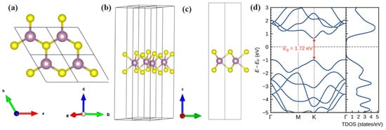
Monolayer MoS2 adopts a hexagonal lattice in which each Mo atomic plane is covalently bonded to two S planes, forming an S-Mo-S sandwich, as illustrated in Figure 1a–c. The electronic band structure and the corresponding total density of states (DOS) shown in Figure 1d reveal a direct band gap of 1.72 eV at the K point, in close agreement with the experimental value of 1.80 eV [63]. This direct band gap implied that optical transitions from the valence band (VB) to the conduction band (CB) occur without a change in crystal momentum, a hallmark of efficient light-matter interaction in 2D semiconductors. The emergence of this direct band gap is intrinsically linked to the absence of interlayer coupling, as the system consists of a single, electronically isolated MoS2 sheet.
Figure 1.
Lattice structure and electronic properties of monolayer MoS2: (a) top view; (b) three-dimensional view; (c) side view of the relaxed hexagonal S-Mo-S lattice (yellow spheres: S atoms; purple spheres: Mo atoms); (d) calculated total DOS and electronic band structure along the high-symmetry path Γ-M-K-Γ, showing a direct band gap of ~1.72 eV at the K point.
The structural parameters of MoS2 were determined using the PBE-GGA functional and are summarized in Table 1. The calculated values show excellent agreement with experimental measurements. providing a robust foundation for subsequent electronic and optical property analyses.
Table 1.
Comparison of lattice parameters of MoS2 monolayer between different approaches and the experiment.
The optical response of monolayer MoS2 was investigated over the 350–1000 nm spectral range, with a focus on its complex dielectric function, which fundamentally dictates the material’s interaction with electromagnetic radiation. As a central descriptor of light-matter coupling, the dielectric function governs excitonic effects, absorption resonances, and overall optoelectronic performance. The real εr(ω), and imaginary εi(ω), components of ε(ω) were extracted using the Kramers–Kronig transformation, providing a rigorous and internally consistent framework for quantifying the optical behavior of MoS2 at the monolayer limit [67]. The complex dielectric function is expressed as:
The real component of the dielectric function, εr(ω) describes the polarization response of the material under an external electromagnetic field, whereas the imaginary component, εi(ω), quantifies the dissipative part of the interaction, providing direct insight into the material’s light-absorption capability. Several key optical properties, including the refractive index n(ω), extinction coefficient k(ω), absorption coefficient α(ω), and reflectance R(ω), can be derived directly from these dielectric components. The absorption coefficient α(ω) specifies the rate at which light intensity decays as it propagates through the material and is directly governed by both k(ω) and the photon energy. Likewise, the reflectance R(ω) at the material surface depends on the combined contributions of n(ω) and k(ω). All these quantities were evaluated using the following standard relationships [68,69,70]:
where c is the speed of light in a vacuum and ω representing the frequency of the incident wave.
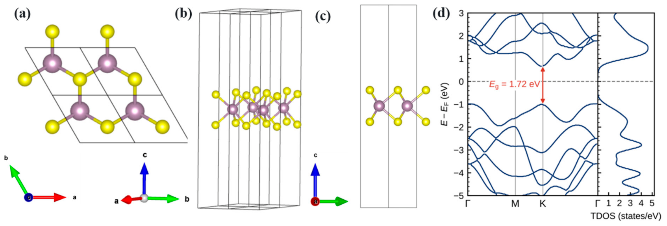
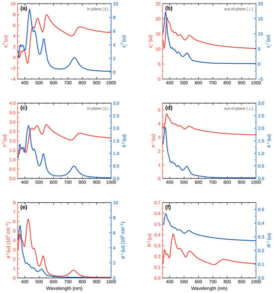
The real and imaginary components of the dielectric function of monolayer MoS2, evaluated along both the in-plane (parallel) and out-of-plane (perpendicular) directions, are presented in Figure 2a,b.
Figure 2.
Real and imaginary components of dielectric constant of MoS2 monolayer: (a) along the parallel direction; (b) along the vertical direction. Refractive index and extinction coefficient: (c) along the parallel direction; (d) along the vertical direction. (e) Absorption coefficient; (f) reflectance along the parallel and the vertical direction.
Along the in-plane direction, εi(ω) exhibits a pronounced maximum at 425 nm, consistent with previously reported values [71,72], which indicates strong optical absorption at this wavelength. The corresponding εr(ω) values oscillate between −1 and 8 across the visible region before stabilizing in the infrared, reflecting the dispersive nature of the monolayer’s electronic polarization. In the out-of-plane direction, εi(ω) displays a sharp peak at 380 nm, followed by a secondary maximum near 525 nm, both characteristic of strong optical transitions in the UV–visible range (Figure 2b). Beyond these features, εi(ω) gradually decreases toward zero in the infrared, confirming that monolayer MoS2 acts as an efficient absorber in the UV–vis spectral window while exhibiting minimal absorption at longer wavelengths.
Along the parallel (in-plane) direction of monolayer MoS2, the refractive index n(ω) exhibits a broad peak in the visible region, reaching a maximum of ~2.7 within the range of 450–550 nm. A secondary peak of ~2.5 appears in the near-IR region around 800 nm (Figure 2c). These elevated n(ω) values indicate that light propagates more slowly through the monolayer at these wavelengths, reflecting strong light-matter coupling between the incident electromagnetic field and the Mo-S lattice. This behavior is consistent with prior theoretical studies [72]. In the same in-plane direction, the extinction coefficient k(ω) displays a dominant peak in the visible region with a maximum of ~2.7, followed by a secondary peak near 1.2, before stabilizing at 0.03 in the IR region. Along the vertical (out-of-plane) direction, which corresponds to the monolayer thickness, n(ω) presents a pronounced peak near 380 nm with a maximum value of ~4.7 (Figure 2d). This feature indicates noticeable attenuation of light propagation through the thickness in the UV–visible range. The corresponding k(ω) profile also shows a dominant peak around 370 nm, reaching ~2, confirming significant absorption of UV light. Beyond this region, both n(ω) and k(ω) decrease markedly toward the visible spectrum and subsequently stabilize in the infrared domain. Figure 2e presents the absorption coefficient α(ω) along the parallel direction, showing strong absorption in the UV and visible regions. α(ω) is approximately 2.8 × 105 cm−1 at 350 nm and reaches a maximum of about 6.3 × 105 cm−1 near 425 nm. Beyond this main peak, absorption generally decreases with increasing wavelength, with weaker features around 530 and 740 nm, before becoming very weak in the IR region [46,73,74,75]. Figure 2f illustrates the reflectance R(ω) of monolayer MoS2 along the parallel direction, showing a broad high-reflectance region in the visible spectrum, indicative of substantial light reflection at these wavelengths. Along the perpendicular direction, strong reflectance is similarly observed in the UV region, in agreement with previous studies [76,77].
3.2. Properties of Graphene
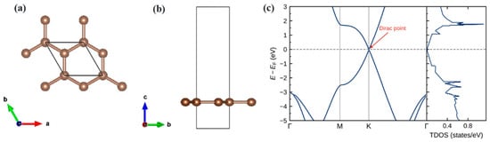
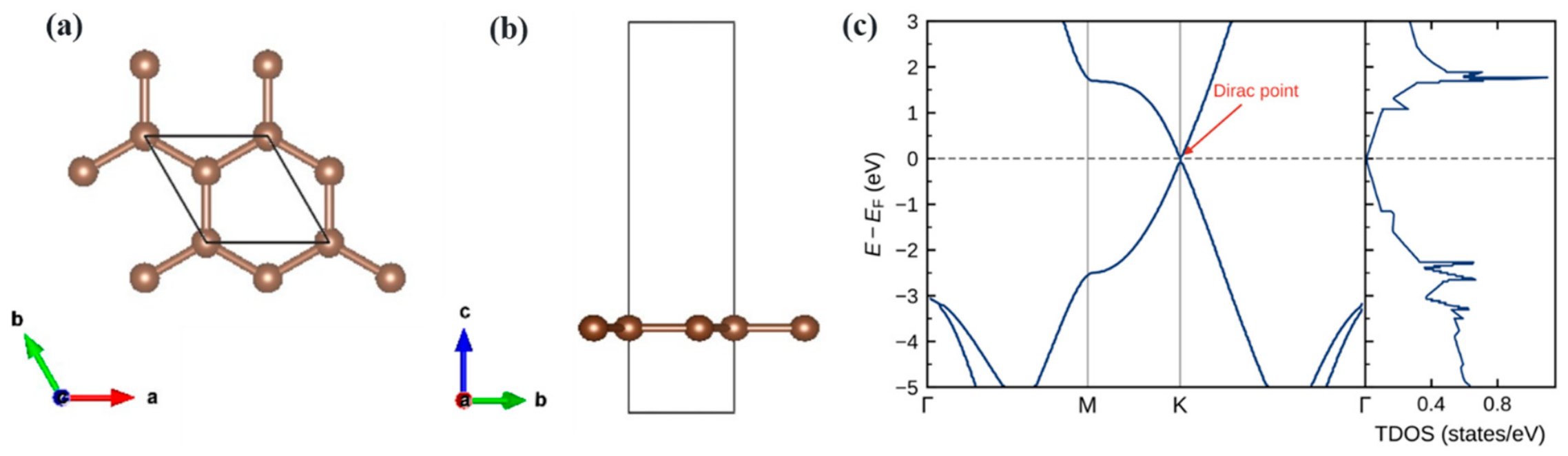
Graphene consists of a single atomic layer of carbon arranged in a 2D hexagonal lattice (Figure 3b), in which each carbon atom forms three σ-bonds with its nearest neighbors, creating the characteristic honeycomb network (Figure 3a). As a first step, the atomic geometry of graphene was optimized so that all subsequent calculations were based on fully relaxed atomic coordinates, thereby minimizing structural defects and enabling accurate prediction of its intrinsic properties. The optimized C-C bond length is 1.42 Å, in excellent agreement with the experimental value [78]. The lattice constant and the cell volume of graphene are a = 2.47 Å and V = 47.44 Å3. According to the DOS and band structure shown in Figure 3c, the CB and VB touch at the K point in the first Brillouin zone, confirming the zero band-gap energy of graphene.
Figure 3.
Crystal structure of Gr: (a) top view, and (b) side view; (c) DOS and band structure of Gr.
3.3. Properties of MoS2/Graphene
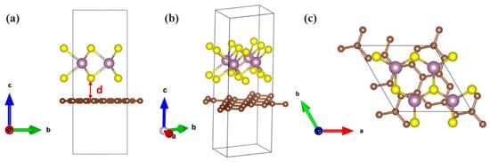
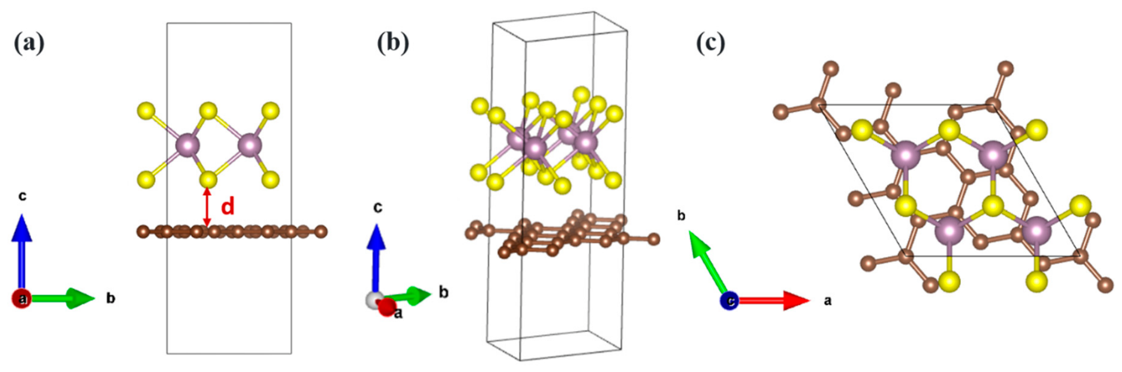
Graphene’s zero-band-gap nature imposes a fundamental limitation on its direct use as a semiconductor in optoelectronic applications. To address this constraint, a van der Waals heterostructure consisting of monolayer MoS2 and graphene was constructed. By systematically tuning the interlayer spacing, we investigated how interfacial coupling modulates the electronic and optical properties of the hybrid system. Figure 4 presents the side, three-dimensional, and top views of the MoS2/graphene heterostructure for interlayer distances ranging from 2.30 Å to 3.20 Å. This controlled variation enables a detailed assessment of the influence of interlayer separation on the emergent electronic characteristics of the combined structure, offering insights into band-engineering strategies for next-generation 2D optoelectronic devices.
Figure 4.
Configuration of MoS2/graphene heterostructure: (a) side view; (b) three-dimensional view; and (c) top view.
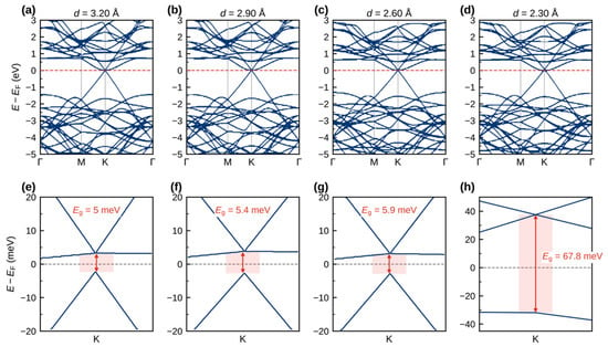
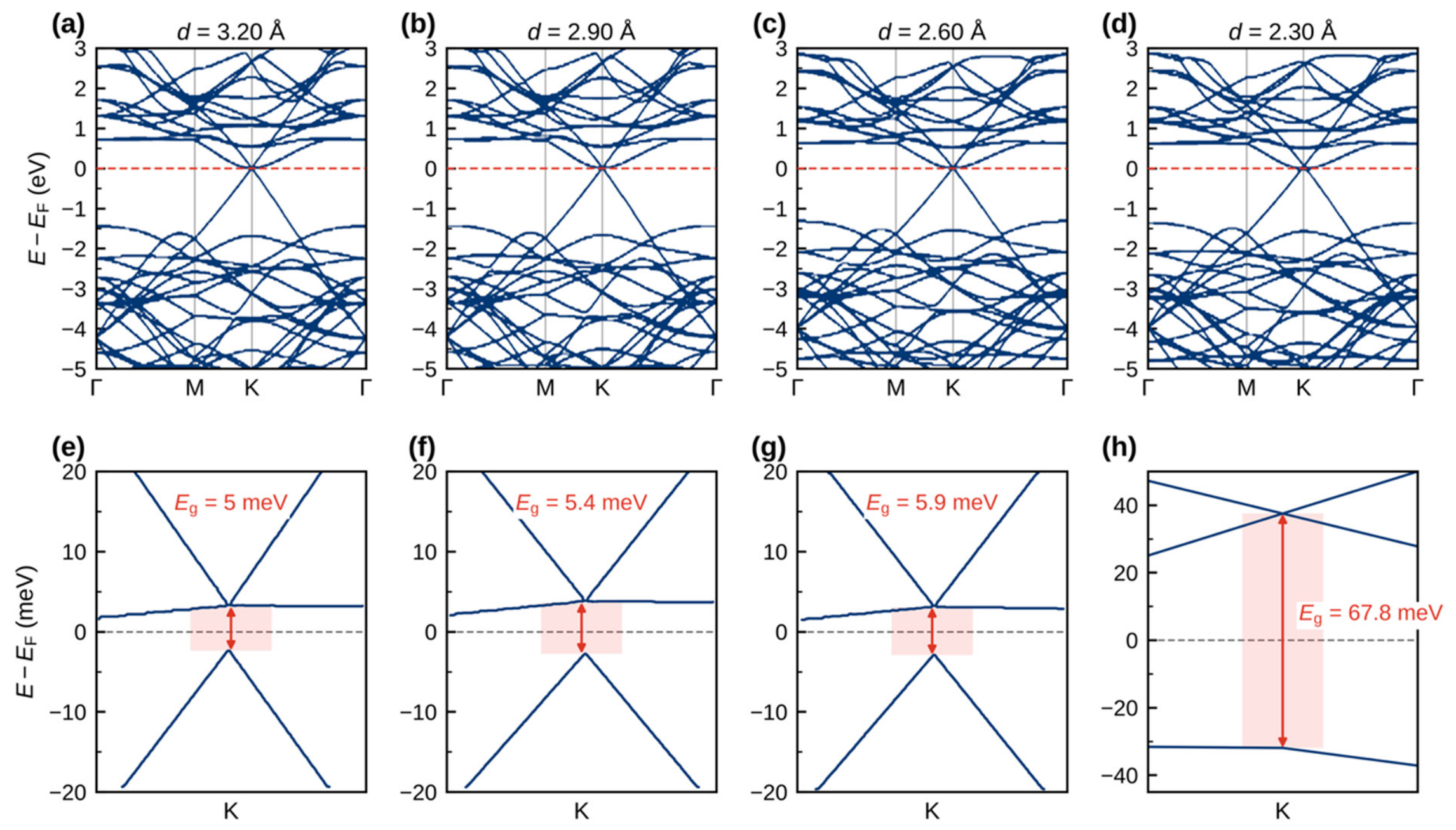
Figure 5a–d present the electronic band structures of the MoS2/graphene heterostructure for each considered interlayer distance. A clear trend emerges, reducing the separation between the MoS2 and graphene layers strengthens the interlayer interaction, which in turn induces progressive shifts in both the CB and VB. As highlighted in the magnified views shown in Figure 5e–h, this enhanced coupling results in a gradual opening of the band gap. The appearance of this gap is most plausibly attributed to modifications in the on-site energies of the carbon atoms in the graphene sheet, arising from the perturbation induced by the adjacent of the MoS2 layer. Such interlayer-coupling-driven band reconfiguration underscores the potential of vdW assembly as an effective strategy for engineering electronic gaps in semi-metallic 2D materials.
Figure 5.
Bands structure of MoS2/graphene heterostructure at various interlayer distances: (a) d = 3.2 Å; (b) d = 2.9 Å; (c) d = 2.6 Å; (d) d = 2.3 Å; (e–h) shows the zoom in of the band structure near fermi energy of 3.2; 2.9; 2.6; and 2.3 Å, respectively.
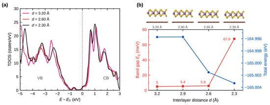
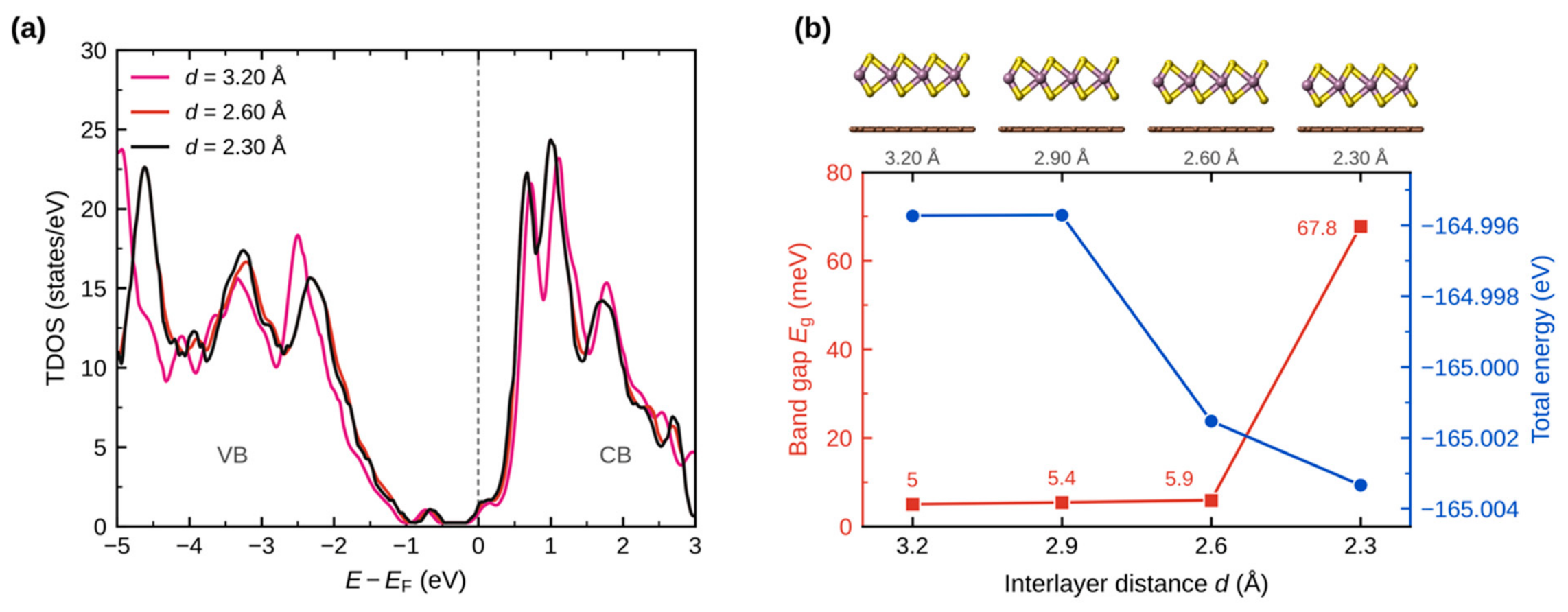
The stacking of MoS2 with graphene enhances interlayer charge transfer, which directly contributes to the opening of a finite band gap in otherwise gapless graphene. Among the converged configurations investigated, the largest band gap, 67.8 meV, was obtained at an interlayer separation of 2.3 Å. In contrast, increasing the spacing to 3.2 Å substantially weakens the electronic coupling, reducing the band gap to 5 meV. This trend is corroborated by the total DOS (TDOS) shown in Figure 6a, as the interlayer distance decreases, a pronounced depletion emerges around the Fermi level. For larger separations, a finite TDOS persists at the Fermi energy, whereas at 2.3 Å the TDOS nearly vanishes, in full agreement with the band-structure analysis, which indicates a widening of the band gap at reduced spacing.
Figure 6.
(a) Total density of states (DOS) of the MoS2/graphene heterostructure at various interlayer distances; (b) band gap energy (red curve) and total energy of the system (blue curve) as a function of interlayer distance.
Figure 6b further supports this interpretation: the total energy of the heterostructure (blue curve) decreases monotonically with decreasing interlayer distance, reaching its lowest value among the converged configurations investigated at 2.3 Å. Calculations at 2.1 and 2.0 Å were performed alongside the other configurations during the original study but did not converge; consequently, these points were excluded from Figure 6b. Enhanced overlap between the S 3p and out-of-plane C 2p orbitals at these compressed separations may contribute to these convergence difficulties. The simultaneous increase in band-gap energy (red curve) and decrease in total energy indicate that the 2.3 Å configuration exhibits both the lowest calculated energy and the largest band gap within the investigated range. However, because this point lies at the boundary of the sampled range, the present results do not establish an equilibrium interlayer separation. Together, these results underscore the strong dependence of the heterostructure’s electronic structure on interlayer coupling strength, highlighting van der Waals spacing as a powerful tuning parameter for band-gap engineering in MoS2/graphene systems.
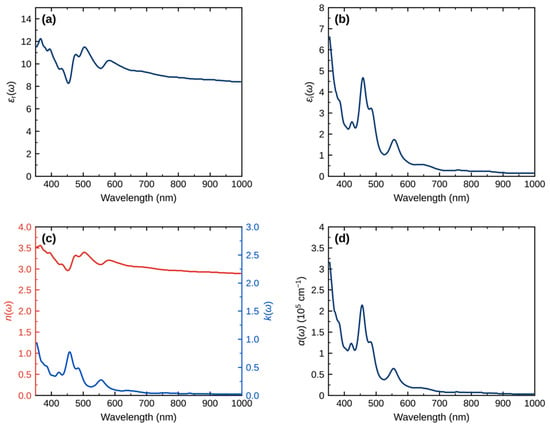
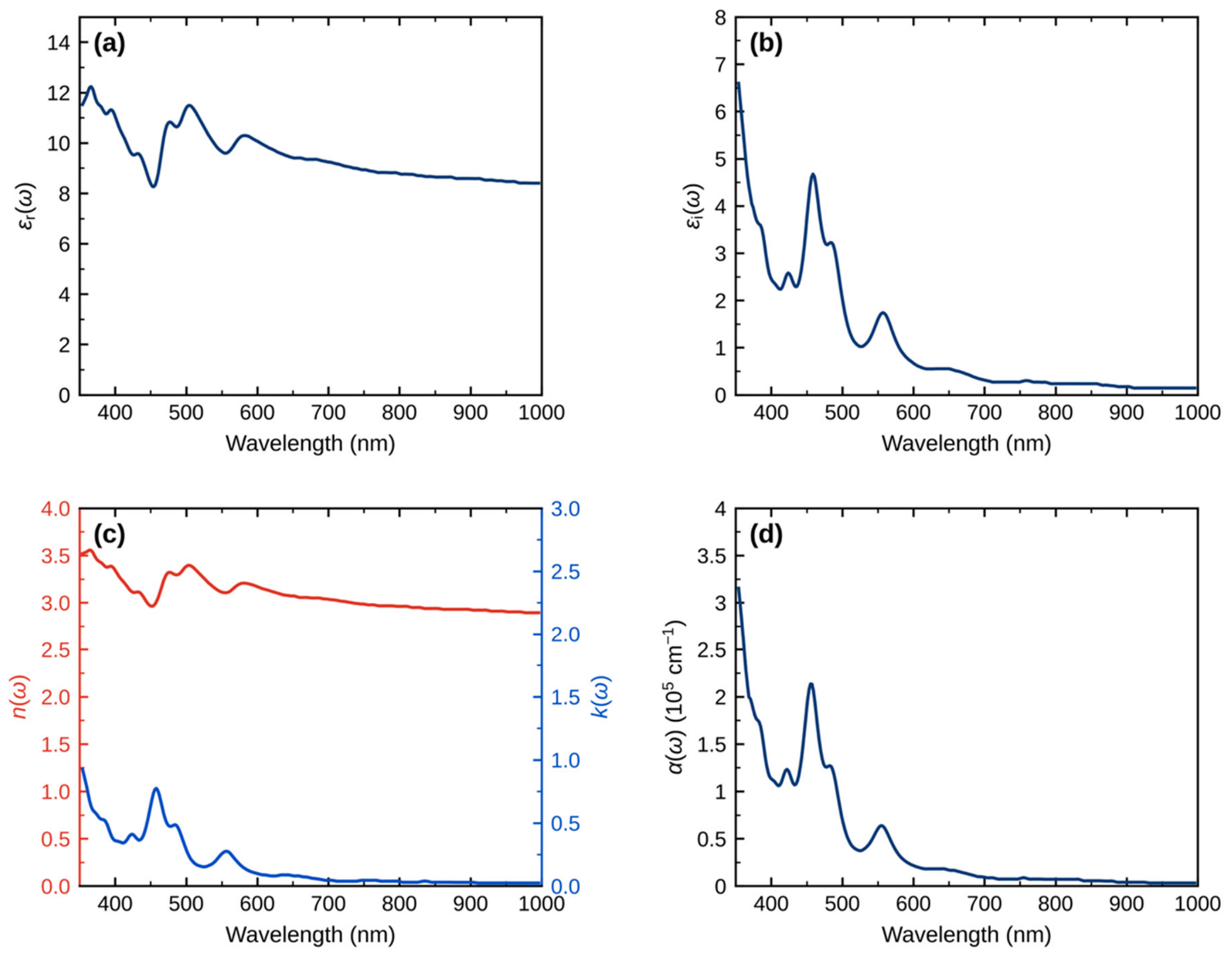
In the following analysis, we focus on the MoS2/graphene heterostructure with an interlayer spacing of 2.3 Å, which is treated as a compressed configuration chosen to probe the effects of enhanced interlayer coupling on the optical properties. The goal is to elucidate how the incorporation of graphene modifies the optical response of MoS2, particularly through the key descriptors ε(ω), n(ω), k(ω), and α(ω). As shown in Figure 7, the real part of the dielectric function, εr(ω), displays pronounced peaks in the UV range (Figure 7a), indicative of enhanced polarization effects under high-energy photon excitation. The imaginary part, εi(ω), likewise exhibits strong UV peaks (Figure 7b), confirming substantial light absorption in this spectral region.
Figure 7.
Optical properties of MoS2/Graphene: (a) dielectric function real component; (b) dielectric function imaginary component; (c) refractive index (red curve) and extinction coefficient (bleu curve); (d) absorption coefficient.
Further insight is provided by the refractive index n(ω) and extinction coefficient k(ω) (Figure 7c,d). Both quantities attain their highest values in the UV, reflecting intensified light-matter interaction and a corresponding reduction in photon group velocity, characteristic of strong optical confinement. The absorption coefficient α(ω) also reaches its maximum in the UV region, where high-amplitude absorption peaks with high amplitudes are observed. Beyond this range, α(ω) decreases sharply across the visible and infrared regions, demonstrating that the optical response of the heterostructure is dominated by UV-driven excitations. At 350 nm in the UV region, the MoS2/graphene heterostructure exhibits an absorption coefficient approximately 1.2 times that of pristine MoS2, corresponding to an increase of about 20%. This pronounced improvement highlights the synergistic interplay between MoS2 and graphene, indicating that interlayer coupling within the heterostructure can significantly amplify optical activity and broaden its applicability for UV-sensitive optoelectronic technologies.
3.4. Gas Sensing
To investigate the adsorption energies (Eads) of selected gas molecules, namely CO2, CO, HF, and NO, on the MoS2/graphene heterostructure, first-principles DFT simulations were performed within the framework of DFT using the PBE-GGA exchange-correlation functional [79]. All calculations were carried out using the Quantum ESPRESSO package [80]. The adsorption energy was computed according to [81]:
where EMoS2/Graphene + Gaz is the total energy of the heterostructure with the gas molecule adsorbed, EMoS2/Graphene is the energy of the pristine heterostructure, and EGaz is the energy of the isolated gas molecule.
Eads = EMoS2/Graphene + Gaz − EMoS2/Graphene − EGaz
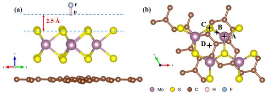
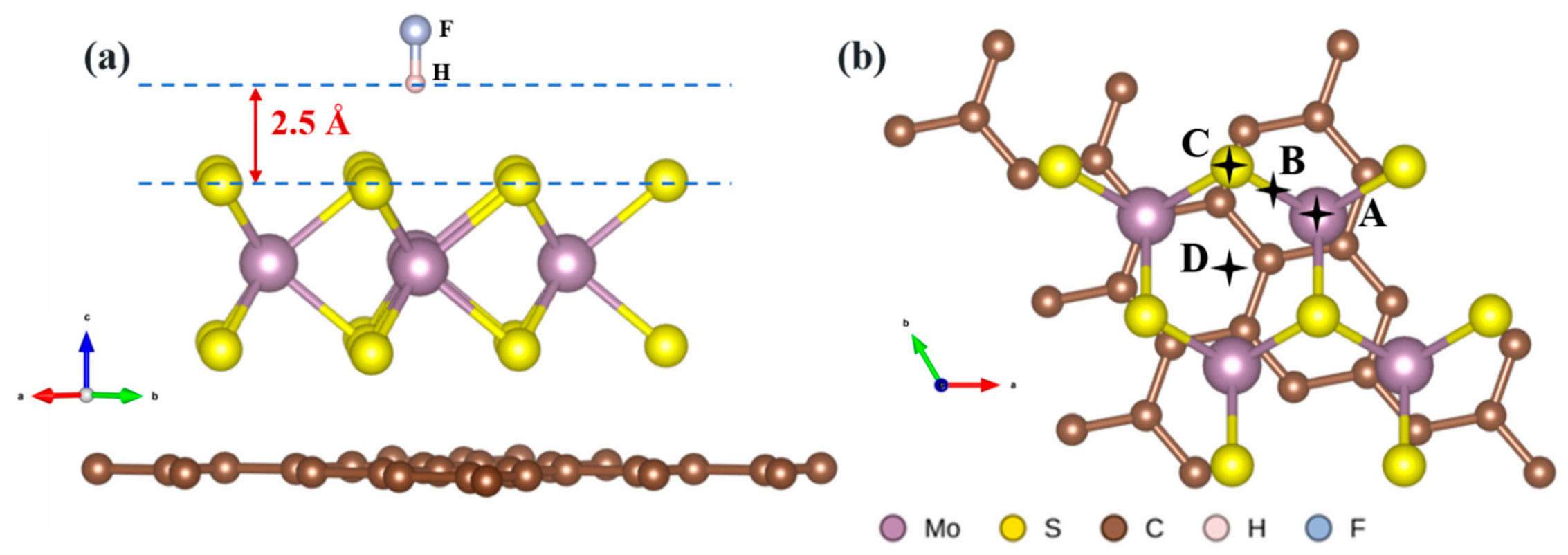
To eliminate spurious interactions between periodic images, a 15 Å vacuum region was introduced perpendicular to the surface to separate periodic images. The initial gas–surface separation was set to 2.5 Å before relaxation. For CO, four initial adsorption sites were investigated (Figure 8b): on top of the Mo atom (A), at the Mo-S bridge site (B), on top of the S atom (C), and at the hollow site at the center of the MoS2 unit cell (D). Site B gave the lowest adsorption energy for CO among the four sites. For CO2, HF, and NO, site B was used as a common starting configuration, followed by structural relaxation.
Figure 8.
Configurations used for gas sensing evaluation: (a) MoS2/Graphene heterostructure used as the basis of the gas sensor; (b) interaction of gas molecules with MoS2/Graphene placed at various positions: (A) above the Mo atom, (B) between the S and Mo atoms, (C) above the S atom and (D) at the center of the MoS2 unit cell.
Using DFT simulations, we investigate the complex gas-detection behavior of our nanostructures toward gas molecules such as CO, CO2, NO, and HF. We aim to uncover subtle structural changes induced by optimization processes and assess their influence on the gas adsorption energies. Table 2 shows the optimized crystalline structures of MoS2 obtained during the adsorption study of CO gas on four distinct sites (A, B, C, and D). For CO2, NO, and HF gases, site B was used as the common starting configuration for structural relaxation. These results are compared with our previous work on MoS2 alone [31].
Table 2.
Structural comparison after adsorption of different gas molecule CO, CO2, NO, and HF at the surface of the MoS2/Graphene.
Table 2 summarizes three key parameters for each gas molecule, the intrinsic bond length of the adsorbate, the equilibrium distance between the molecule and the MoS2/graphene surface, and the corresponding adsorption energy (Eads). For CO, the adsorption energies range from −70 to −62 meV, with site B giving the most negative value (−70 meV) among the four sites examined. Using site B as the common starting configuration, the calculated adsorption energies for CO2, HF, and NO are −51, −127, and −363 meV, respectively. Among the configurations examined, NO shows the strongest binding to the heterostructure, confirming its exceptional sensitivity to the MoS2/graphene surface toward NO. A comparison with the adsorption behavior on the individual materials reveals that the effect of heterostructure formation depends on the nature of the adsorbed gas. On pristine graphene, CO exhibits only weak physisorption (≈−10.2 meV), and on MoS2 the interaction is even weaker (≈−5 meV) at site B. In contrast, adsorption on the MoS2/graphene heterostructure is dramatically strengthened, reaching −70 meV at the same site. A similar enhancement is observed for HF, for which graphene alone yields adsorption energies of about −100 meV, compared with −127 meV on the heterostructure. For NO, the improvement is even more pronounced, where the adsorption on graphene is limited to approximately −29 meV, whereas the heterostructure achieves a much larger interaction energy of −363 meV. For CO2, adsorption is stronger on pristine graphene (−250 meV) than on the heterostructure (−51 meV).
These results demonstrate that integrating graphene with MoS2 leverages the high surface area and conductivity of graphene together with the strong binding affinity of MoS2, producing a synergistic effect that enhances charge transfer and adsorption strength. Consequently, the MoS2/graphene hybrid exhibits significantly improved gas-sensing performance for three of the four hazardous gases investigated with particularly outstanding sensitivity toward NO, consistent with earlier findings [87].
Moreover, the adsorption process induces subtle structural modifications in the gas molecules, including slight bond-length contractions. Structural relaxation also leads to gas-dependent changes in the gas–surface separation: the distance increases for CO, CO2, and NO, whereas it decreases for HF. These differences highlight the influence of the nature of the adsorbed molecule on the structural response of the MoS2/graphene heterostructure and reflect the role of interfacial interactions in modulating adsorption behavior.
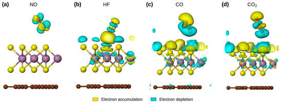
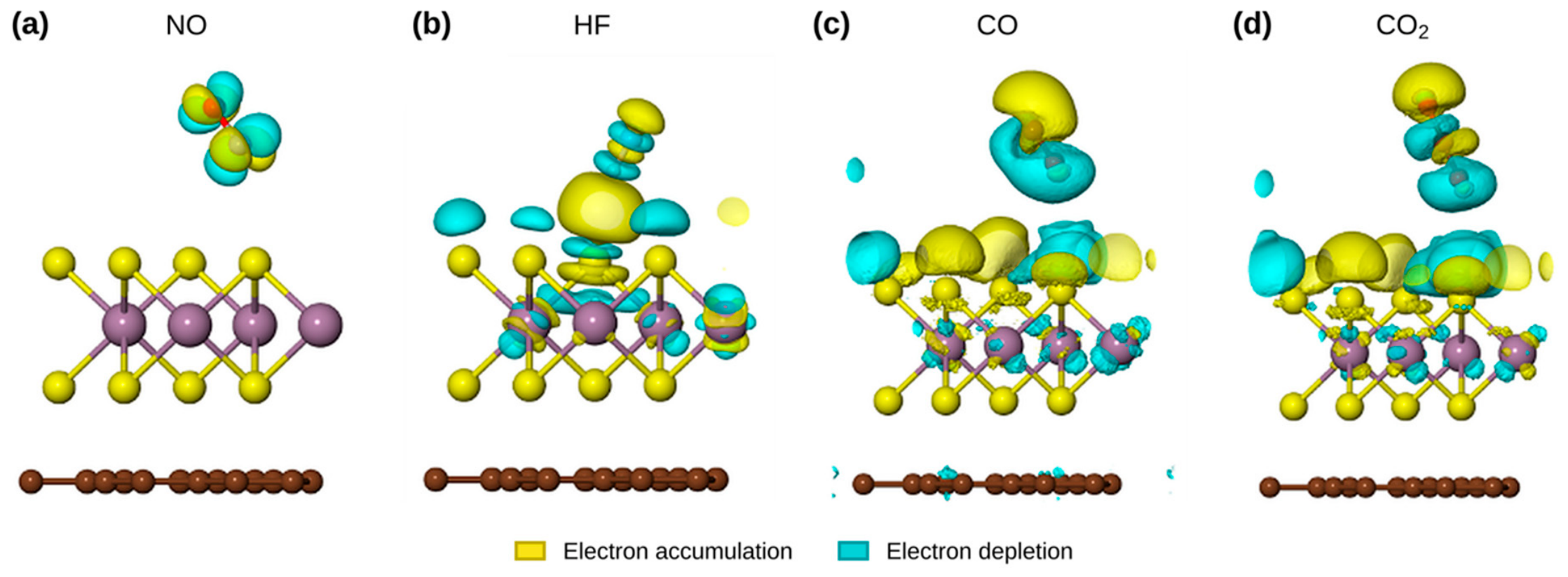
To elucidate the electronic origin of these adsorption responses, Bader charge analysis [88] was performed for all four target molecules on the MoS2/graphene heterostructure (Table 2, Figure 9). The resulting charge-transfer landscape reveals four distinct regimes that correlate directly with both the magnitude of interfacial charge redistribution and the strength of the underlying surface-molecule interaction. For HF, a moderate net charge transfer of approximately 0.036 e from the heterostructure to the molecule is observed, identifying HF as a weak electron acceptor. The accumulated electron density is preferentially localized on the fluorine atom, consistent with its high electronegativity, and the overall pattern is characteristic of a predominantly physisorptive interaction. In contrast, both CO and CO2 display essentially negligible charge transfer of approximately 0.005 e, confirming their behavior as very weak electron acceptors whose adsorption is governed almost entirely by van der Waals forces, with CO coupling to the surface even more weakly than HF.
Figure 9.
Charge density difference for gas molecules (a) NO, (b) HF, (c) CO and (d) CO2 adsorbed on MoS2/Graphene heterostructure. Yellow and cyan isosurfaces denote electron accumulation (Δρ > 0) and depletion (Δρ < 0), respectively. The positive and negative isosurfaces were plotted with magnitudes of (a) 2.8 × 10⁻³, (b) 4.0 × 10⁻⁴, (c) 2.0 × 10⁻⁵ and (d) 3.0 × 10⁻⁵ e Bohr−3.
A markedly different regime is observed for NO, which exhibits a substantially higher charge transfer of approximately 0.057 e, identifying it as a strong electron acceptor. The transferred density is concentrated on the nitrogen atom, signaling partial occupation of NO’s antibonding π* orbital and pointing to a more covalent, hybridized interaction with the heterostructure. The NO-MoS2/graphene system therefore approaches a chemisorption-like regime, a behavior attributable to the radical (open-shell) electronic structure of NO and the resulting orbital availability for charge exchange.
Considered collectively, the Bader analysis establishes a clear hierarchy of interfacial activity, NO ≫ HF > CO2 ≈ CO, in which NO emerges as both the most strongly bound and the most electronically perturbing analyte. This hierarchy mirrors the trend observed in the adsorption-energy data discussed above, providing internally consistent computational evidence that the selectivity of MoS2/graphene heterostructures toward radical, redox-active species is governed not by geometric accessibility alone, but by the orbital-resolved charge-transfer pathways enabled at the heterointerface. This insight is directly relevant to the rational design of selective electronic noses and chemiresistive sensors.
Figure 9 visualizes the charge-density difference (CDD) maps obtained upon adsorption of (a) NO, (b) HF, (c) CO, and (d) CO2 on the MoS2/graphene heterostructure, where the yellow and cyan iso-surfaces denote regions of charge accumulation and depletion, respectively. The CDD distributions provide a real-space counterpart to the Bader analysis discussed above and resolve four distinct interfacial coupling regimes. In panel (a), NO induces a pronounced and spatially extended charge redistribution, with strong localization across both the molecule and the underlying MoS2/graphene region, a hallmark of chemisorption-like coupling driven by the radical (open-shell) electronic structure of NO. In panel (b), HF produces a moderate redistribution that is preferentially concentrated around the fluorine atom, reflecting its role as a weak electron acceptor whose binding remains largely physisorptive. By contrast, panels (c) and (d) reveal that CO and CO2 generate only faint and diffuse redistribution patterns, consistent with negligible interfacial electron transfer and a purely physisorbed regime. The integrated CDD response therefore follows the hierarchy NO > HF > CO ≈ CO2, in full quantitative agreement with the Bader-derived charge-transfer trend, and unambiguously identifies NO as the analyte that most strongly perturbs the electronic structure of the MoS2/graphene heterointerface. To determine whether this preferential coupling is preserved in realistic gas mixtures, additional calculations were performed in which a NO molecule was introduced in the presence of CO2 as a co-adsorbate. Under these conditions, the adsorption energy of NO is computed to be −294.6 meV, only modestly reduced relative to its isolated value of −363 meV. This limited destabilization (≈19% reduction in binding strength) demonstrates that the presence of CO2 does not meaningfully disrupt the NO-surface interaction, and that the active sites of MoS2 within the heterostructure retain their pronounced affinity for NO even in a CO2-rich atmosphere. This behavior is mechanistically consistent with the substantially stronger interfacial charge transfer for NO (0.057 e), approximately 11 times that for CO2 (0.005 e), which is approximately 11 times higher. This difference suggests stronger electronic coupling between NO and the MoS2/graphene heterostructure, whereas CO2 exhibits weaker charge transfer and less pronounced interfacial interactions. These findings establish that the MoS2/graphene heterostructure exhibits a high intrinsic selectivity toward NO, robust against CO2 interference, and they reinforce its potential as a foundational platform for selective, low-cross-talk, room-temperature gas-sensing devices for environmental, industrial, and biomedical monitoring applications.
4. Conclusions
In summary, this work provides a comprehensive first-principles DFT investigation of the structural, electronic, optical, and gas-sensing properties of a MoS2/graphene van der Waals heterostructure. Our analysis demonstrates that tuning the interlayer spacing serves as an effective strategy for engineering a finite band gap in graphene, with a maximum value of 67.8 meV at a separation of 2.3 Å. This proximity-induced modulation of the electronic structure is further supported by the depletion of the DOS at the Fermi level and the concurrent reduction in total energy. Such control over gap opening is essential for enabling the integration of graphene into semiconducting, optoelectronic, and photonic platforms. The optical analysis reveals that the MoS2/graphene heterostructure exhibits an absorption coefficient approximately 1.2 times that of pristine MoS2, corresponding to an increase of about 20% at 350 nm. driven by stronger polarization, increased dielectric response, and intensified light-matter coupling at short wavelengths. This improved optical performance highlights the potential of the heterostructure for UV photodetectors, optical modulators, and energy-harvesting devices. Equally important is the heterostructure’s potential for gas-sensing applications, as suggested by the calculated adsorption energies. Among the gases studied (CO, CO2, NO, HF), NO exhibits the strongest adsorption, reaching −363 meV, which far exceeds the values obtained for pristine graphene or MoS2. The dramatic enhancement in adsorption energy, e.g., from −29 meV on graphene to −363 meV on the heterostructure, demonstrates a strong synergistic interplay between graphene’s high conductivity and MoS2’s strong binding affinity. This synergy leads to improved charge transfer, deeper potential wells, and structurally responsive adsorption geometries. These theoretical findings suggest that the MoS2/graphene heterostructure is a promising candidate for gas sensing, with preferential NO adsorption among the gases investigated. Experimental validation represents an important direction for future work to assess its sensitivity, selectivity, and performance under realistic operating conditions.
Author Contributions
A.B. (Abderrahim Bayou), A.K., M.A., A.A.-S. and E.M.N. investigation, formal analysis, writing—original draft, A.B. (Abdelkrim Batan) data curation, validation, B.A., B.H. and M.J. conceptualization, validation, supervision. All the authors contributed equally to writing and reviewing the manuscript. All authors have read and agreed to the published version of the manuscript.
Funding
This research received no external funding.
Institutional Review Board Statement
Not applicable.
Informed Consent Statement
Not applicable.
Data Availability Statement
All data of this work are made available from the corresponding author upon request.
Acknowledgments
The authors are grateful to the Region of HDF for financial support.
Conflicts of Interest
The authors declare no conflicts of interest.
References
- Novoselov, K.S. Nobel Lecture: Graphene: Materials in the Flatland. Rev. Mod. Phys. 2011, 83, 837–849. [Google Scholar] [CrossRef] [Scilit]
- Zhang, S.; Wang, H.; Liu, J.; Bao, C. Measuring the specific surface area of monolayer graphene oxide in water. Mater. Lett. 2020, 261, 127098. [Google Scholar] [CrossRef] [Scilit]
- Zheng, C.; Zhou, X.; Cao, H.; Wang, G.; Liu, Z. Synthesis of porous graphene/activated carbon composite with high packing density and large specific surface area for supercapacitor electrode material. J. Power Sources 2014, 258, 290–296. [Google Scholar] [CrossRef] [Scilit]
- Papageorgiou, D.G.; Kinloch, I.A.; Young, R.J. Mechanical properties of graphene and graphene-based nanocomposites. Prog. Mater. Sci. 2017, 90, 75–127. [Google Scholar] [CrossRef] [Scilit]
- Pang, Y.; Yang, J.; Curtis, T.E.; Luo, S.; Huang, D.; Feng, Z.; Morales-Ferreiro, J.O.; Sapkota, P.; Lei, F.; Zhang, J.; et al. Exfoliated Graphene Leads to Exceptional Mechanical Properties of Polymer Composite Films. ACS Nano 2019, 13, 1097–1106. [Google Scholar] [CrossRef] [Scilit] [PubMed]
- Yang, K.; Wu, C.; Zhang, G. A state of review for graphene-based materials in preparation methods, characterization, and properties. Mater. Sci. Eng. B 2024, 310, 117698. [Google Scholar] [CrossRef] [Scilit]
- Shekhawat, A.; Ritchie, R.O. Toughness and strength of nanocrystalline graphene. Nat. Commun. 2016, 7, 10546. [Google Scholar] [CrossRef] [Scilit] [PubMed]
- Park, W.-Y.; Han, J.; Moon, J.; Joo, S.; Wada, T.; Ichikawa, Y.; Ogawa, K.; Kim, H.S.; Chen, M.; Kato, H. Mechanically Robust Self-Organized Crack-Free Nanocellular Graphene with Outstanding Electrochemical Properties in Sodium Ion Battery. Adv. Mater. 2024, 36, 2311792. [Google Scholar] [CrossRef] [Scilit] [PubMed]
- Lim, M.; Kim, H.-D.; Shim, H.C.; Kim, K.-S.; An, B.-S.; Kim, J.-H. Optically transparent and infrared tunable flexible camouflage device. Nano Energy 2024, 131, 110189. [Google Scholar] [CrossRef] [Scilit]
- Gosling, J.H.; Makarovsky, O.; Wang, F.; Cottam, N.D.; Greenaway, M.T.; Patanè, A.; Wildman, R.D.; Tuck, C.J.; Turyanska, L.; Fromhold, T.M. Universal mobility characteristics of graphene originating from charge scattering by ionised impurities. Commun. Phys. 2021, 4, 30. [Google Scholar] [CrossRef] [Scilit]
- Guo, W.; Zhang, M.; Xue, Z.; Chu, P.K.; Mei, Y.; Tian, Z.; Di, Z. Extremely High Intrinsic Carrier Mobility and Quantum Hall Effect Of Single Crystalline Graphene Grown on Ge(110). Adv. Mater. Interfaces 2023, 10, 2300482. [Google Scholar] [CrossRef] [Scilit]
- Zhou, W.; Ma, T.; Tian, Y.; Jiang, Y.; Yu, X. Dielectric engineered graphene transistors for high-performance near-infrared photodetection. iScience 2024, 27, 109314. [Google Scholar] [CrossRef] [Scilit] [PubMed]
- Kotbi, A.; Lejeune, M.; Oughaddou, H.; Rajput, N.; Zhang, X.; Belhadi, J.; Zakaria, Y.; Richert, D.; Piquemal, F.; Morán-Meza, J.; et al. Eco-Friendly Deposition of Catalyst-Free Graphene on Diverse Substrates. Adv. Sustain. Syst. 2025, 9, 2500105. [Google Scholar] [CrossRef] [Scilit]
- Mouloua, D.; Kotbi, A.; Deokar, G.; Kaja, K.; El Marssi, M.; EL Khakani, M.A.; Jouiad, M. Recent Progress in the Synthesis of MoS2 Thin Films for Sensing, Photovoltaic and Plasmonic Applications: A Review. Materials 2021, 14, 3283. [Google Scholar] [CrossRef] [Scilit] [PubMed]
- Getaneh, S.A.; Temam, A.G.; Workneh, G.A.; Nwanya, A.C.; Ejikeme, P.M.; Ezema, F.I. Advances in MoS2-Based ternary nanocomposites for high-performance electrochemical energy storage. Hybrid Adv. 2024, 7, 100333. [Google Scholar] [CrossRef] [Scilit]
- Ouyang, W.; Sofer, R.; Gao, X.; Hermann, J.; Tkatchenko, A.; Kronik, L.; Urbakh, M.; Hod, O. Anisotropic Interlayer Force Field for Transition Metal Dichalcogenides: The Case of Molybdenum Disulfide. J. Chem. Theory Comput. 2021, 17, 7237–7245. [Google Scholar] [CrossRef] [Scilit] [PubMed]
- Raghunathan, M.; Kapoor, A.; Kumar, P.; Laxshmivarahan, A.; Tripathi, S.C.; Ahmad, I.; Pal, D.B. Nanostructured transition metal dichalcogenides-based colorimetric sensors: Synthesis, characterization, and emerging applications. Luminescence 2024, 39, e4833. [Google Scholar] [CrossRef] [Scilit] [PubMed]
- Szary, M.J.; Radomski, P. Unveiling the Chemical Underpinnings behind the Enhanced Adsorption Interaction of NO2 on MoS2, MoSe2, and MoTe2 Transition Metal Dichalcogenides. J. Phys. Chem. C 2023, 127, 21374–21386. [Google Scholar] [CrossRef] [Scilit]
- Obodo, P.C.; Obodo, K.O.; Aigbe, U.O.; Aigbodion, V. Recent Advances in Molybdenum Disulfide (MoS2) and MXene-based Heterostructures for Photovoltaic and Water Splitting Applications: A Review. ChemistrySelect 2025, 10, e202404995. [Google Scholar] [CrossRef] [Scilit]
- Coutinho, S.S.; Tavares, M.S.; Barboza, C.A.; Frazão, N.F.; Moreira, E.; Azevedo, D.L. 3R and 2H polytypes of MoS2: DFT and DFPT calculations of structural, optoelectronic, vibrational and thermodynamic properties. J. Phys. Chem. Solids 2017, 111, 25–33. [Google Scholar] [CrossRef] [Scilit]
- Banu, S.L.; Veerapandy, V.; Fjellvåg, H.; Vajeeston, P. First-Principles Insights into the Relative Stability, Physical Properties, and Chemical Properties of MoSe2. ACS Omega 2023, 8, 13799–13812. [Google Scholar] [CrossRef] [Scilit] [PubMed]
- Gu, M.; Rao, A.M.; Zhou, J.; Lu, B. Molecular modulation strategies for two-dimensional transition metal dichalcogenide-based high-performance electrodes for metal-ion batteries. Chem. Sci. 2024, 15, 2323–2350. [Google Scholar] [CrossRef] [Scilit] [PubMed]
- Thayil, R.; Parne, S.R.; Ramana, C.V. 2D MoS2 for Next-Generation Electronics and Optoelectronics: From Material Properties to Manufacturing Challenges and Future Prospects. Small 2025, 21, 2412467. [Google Scholar] [CrossRef] [Scilit] [PubMed]
- Jones, L.A.H.; Xing, Z.; Swallow, J.E.N.; Shiel, H.; Featherstone, T.J.; Smiles, M.J.; Fleck, N.; Thakur, P.K.; Lee, T.-L.; Hardwick, L.J.; et al. Band Alignments, Electronic Structure, and Core-Level Spectra of Bulk Molybdenum Dichalcogenides (MoS2, MoSe2, and MoTe2). J. Phys. Chem. C 2022, 126, 21022–21033. [Google Scholar] [CrossRef] [Scilit] [PubMed]
- Mir, S.H.; Yadav, V.K.; Singh, J.K. Recent Advances in the Carrier Mobility of Two-Dimensional Materials: A Theoretical Perspective. ACS Omega 2020, 5, 14203–14211. [Google Scholar] [CrossRef] [Scilit] [PubMed]
- Schmidt, H.; Wang, S.; Chu, L.; Toh, M.; Kumar, R.; Zhao, W.; Neto, A.H.C.; Martin, J.; Adam, S.; Özyilmaz, B.; et al. Transport Properties of Monolayer MoS2 Grown by Chemical Vapor Deposition. Nano Lett. 2014, 14, 1909–1913. [Google Scholar] [CrossRef] [Scilit] [PubMed]
- Zhao, X.; Perry, S.S. The Role of Water in Modifying Friction within MoS2 Sliding Interfaces. ACS Appl. Mater. Interfaces 2010, 2, 1444–1448. [Google Scholar] [CrossRef] [Scilit] [PubMed]
- Kabir, M.H.; Dias, D.; Marjuban, S.M.H.; Avais, M.; Castaneda, H.; Liang, H. Effects of urea-functionalized MoS2 on hydrophilic lubrication. Tribol. Int. 2025, 203, 110384. [Google Scholar] [CrossRef] [Scilit]
- Tian, X.; Wang, S.; Li, H.; Li, M.; Chen, T.; Xiao, X.; Wang, Y. Recent advances in MoS2-based nanomaterial sensors for room-temperature gas detection: A review. Sens. Diagn. 2023, 2, 361–381. [Google Scholar] [CrossRef] [Scilit]
- Liu, H.; Zhang, S.; Cheng, Q.; Wang, L.; Wang, S. A Mini Review on the Recent Progress of MoS2-Based Gas Sensors. Catal. Lett. 2024, 154, 1375–1384. [Google Scholar] [CrossRef] [Scilit]
- Alqaydi, M.; Kotbi, A.; Rajput, N.S.; Bouchalkha, A.; Gagou, Y.; El Marssi, M.; Kasmi, C.; Jouiad, M. Gas sensing capabilities of MoS2 and WS2: Theoretical and experimental study. Emergent Mater. 2025, 8, 5799–5811. [Google Scholar] [CrossRef] [Scilit]
- Yan, L.; Shi, H.; Sui, X.; Deng, Z.; Gao, L. MoS2-DNA and MoS2 based sensors. RSC Adv. 2017, 7, 23573–23582. [Google Scholar] [CrossRef] [Scilit]
- Nguyen, S.H.; Vu, P.K.T.; Tran, M.T. Absorbance biosensors-based hybrid MoS2 nanosheets for Escherichia coli detection. Sci. Rep. 2023, 13, 10235. [Google Scholar] [CrossRef] [Scilit] [PubMed]
- Zhao, L.; Wang, Y.; Wei, C.; Huang, X.; Zhang, X.; Wen, G. MoS2-based anode materials for lithium-ion batteries: Developments and perspectives. Particuology 2024, 87, 240–270. [Google Scholar] [CrossRef] [Scilit]
- Yoo, J.; Zewdie, G.M.; Shin, H. Advancements in MoS2-based anodes for Li-ion batteries: Recent progress, challenges, and future directions. Inorg. Chem. Front. 2025, 12, 2587–2612. [Google Scholar] [CrossRef] [Scilit]
- Xu, Y.; Wang, Y.; Zhang, C.; Wu, H.; Tan, C.; Hu, G.; Wang, Z. The role of trap states in MoS2-based photodetectors. Nanoscale 2025, 17, 9245–9252. [Google Scholar] [CrossRef] [Scilit] [PubMed]
- Kwak, D.; Polyushkin, D.K.; Mueller, T. In-sensor computing using a MoS2 photodetector with programmable spectral responsivity. Nat. Commun. 2023, 14, 4264. [Google Scholar] [CrossRef] [Scilit] [PubMed]
- Bayou, A.; Asbani, B.; Rajput, N.; Mouloua, D.; Campos, A.; Lahmar, A.; Hoummada, K.; Ouaghaddou, H.; Zhang, X.; El Marssi, M.; et al. Unlocking Superior Photodetection Properties of Electrodeposited MoS2 Quantum Dots. Small 2025, 21, e08001. [Google Scholar] [CrossRef] [Scilit] [PubMed]
- Alfa, I.; Hafeez, H.Y.; Mohammed, J.; Abdu, S.; Suleiman, A.B.; Ndikilar, C.E. A recent progress and advancement on MoS2-based photocatalysts for efficient solar fuel (hydrogen) generation via photocatalytic water splitting. Int. J. Hydrog. Energy 2024, 71, 1006–1025. [Google Scholar] [CrossRef] [Scilit]
- Das, S.; Acharya, L.; Biswal, L.; Parida, K. Augmented photocatalysis induced by 1T-MoS2 bridged 2D/2D MgIn2S4@1T/2H-MoS2 Z-scheme heterojunction: Mechanistic insights into H2O2 and H2 evolution. Nanoscale Adv. 2024, 6, 934–946. [Google Scholar] [CrossRef] [Scilit] [PubMed]
- Bayou, A.; Asbani, B.; Doubi, Y.; Rajput, N.; Campos, A.; El Marssi, M.; Jouiad, M. Superior photoelectrochemical performance of electrodeposited 1T/2H–MoS2 quantum dots for hydrogen evolution. Int. J. Hydrog. Energy 2025, 139, 107–115. [Google Scholar] [CrossRef] [Scilit]
- Bayou, A.; Asbani, B.; Guilbert, G.; Rajput, N.; Lahem, D.; Jouiad, M. Interface-engineered 1T/2H-MoS2 on 3D nickel foam enables accelerated hydrogen evolution kinetics. Int. J. Hydrog. Energy 2026, 266, 157065. [Google Scholar] [CrossRef] [Scilit]
- Anushya, G.; Benjamin, M.; Sarika, R.; Pravin, J.C.; Sridevi, R.; Nirmal, D. A review on applications of molybdenum disulfide material: Recent developments. Micro Nanostructures 2024, 186, 207742. [Google Scholar] [CrossRef] [Scilit]
- Im, H.; Kim, J.; Kim, J.; Kim, S. Scalable Bilayer MoS2-Based Vertically Inverted p–i–n Light-Emitting Diodes. Adv. Mater. Interfaces 2024, 11, 2300319. [Google Scholar] [CrossRef] [Scilit]
- Asbani, B.; Doubi, Y.; Bayou, A.; Rajput, N.; Jouiad, M. MoS2 quantum dots based next-generation micro-supercapacitors. J. Energy Storage 2026, 153, 121060. [Google Scholar] [CrossRef] [Scilit]
- Tan, F.; Li, J.; Fang, X.; Guan, L. The optical properties of few-layer MoS2 by DFT calculations. Physica E Low. Dimens. Syst. Nanostruct. 2024, 155, 115813. [Google Scholar] [CrossRef] [Scilit]
- Gusakova, J.; Wang, X.; Shiau, L.L.; Krivosheeva, A.; Shaposhnikov, V.; Borisenko, V.; Gusakov, V.; Tay, B.K. Electronic Properties of Bulk and Monolayer TMDs: Theoretical Study Within DFT Framework (GVJ-2e Method). Phys. Status Solidi A 2017, 214, 1700218. [Google Scholar] [CrossRef] [Scilit]
- Bayou, A.; Asbani, B.; Kotbi, A.; Lejeune, M.; Rajput, N.; Doubi, Y.; Jouiad, M. Mixed-phase electrodeposited MoS2 quantum dots for solar-driven dye removal. J. Photochem. Photobiol. A Chem. 2026, 474, 116987. [Google Scholar] [CrossRef] [Scilit]
- Conley, H.J.; Wang, B.; Ziegler, J.I.; Haglund, R.F., Jr.; Pantelides, S.T.; Bolotin, K.I. Bandgap Engineering of Strained Monolayer and Bilayer MoS2. Nano Lett. 2013, 13, 3626–3630. [Google Scholar] [CrossRef] [Scilit] [PubMed]
- Ulian, G.; Valdrè, G. Facile band gap tuning in graphene–brucite heterojunctions. Sci. Rep. 2023, 13, 23090. [Google Scholar] [CrossRef] [Scilit] [PubMed]
- Thomas, N.; Mathew, S.; Nair, K.; O’DOwd, K.; Forouzandeh, P.; Goswami, A.; McGranaghan, G.; Pillai, S. 2D MoS2: Structure, mechanisms, and photocatalytic applications. Mater. Today Sustain. 2021, 13, 100073. [Google Scholar] [CrossRef] [Scilit]
- Zhang, Y.; Zhao, H.L.; Huang, S.; Hossain, M.A.; van der Zande, A.M. Enhancing Carrier Mobility in Monolayer MoS2 Transistors with Process-Induced Strain. ACS Nano 2024, 18, 12377–12385. [Google Scholar] [CrossRef] [Scilit] [PubMed]
- Cheng, Z.; He, S.; Han, X.; Zhang, X.; Chen, L.; Duan, S.; Zhang, S.; Xia, M. Improving electron mobility in MoS2 field-effect transistors by optimizing the interface contact and enhancing the channel conductance through local structural phase transition. J. Mater. Chem. C 2024, 12, 2794–2802. [Google Scholar] [CrossRef] [Scilit]
- Kandhasamy, D.M.; Muthu Mareeswaran, P.; Chellappan, S.; Namasivayam, D.; Aldahish, A.; Chidambaram, K. Synthesis and Photoluminescence Properties of MoS2/Graphene Heterostructure by Liquid-Phase Exfoliation. ACS Omega 2022, 7, 629–637. [Google Scholar] [CrossRef] [Scilit] [PubMed]
- Chang, K.; Chen, W. L-Cysteine-Assisted Synthesis of Layered MoS2/Graphene Composites with Excellent Electrochemical Performances for Lithium Ion Batteries. ACS Nano 2011, 5, 4720–4728. [Google Scholar] [CrossRef] [Scilit] [PubMed]
- Li, Y.; Wang, H.; Xie, L.; Liang, Y.; Hong, G.; Dai, H. MoS2 Nanoparticles Grown on Graphene: An Advanced Catalyst for the Hydrogen Evolution Reaction. J. Am. Chem. Soc. 2011, 133, 7296–7299. [Google Scholar] [CrossRef] [Scilit] [PubMed]
- Vu, S.; Siaj, M.; Izquierdo, R. Graphene-Based Fiber Materials for Gas Sensing Applications: State of the Art Review. Materials 2024, 17, 5825. [Google Scholar] [CrossRef] [Scilit] [PubMed]
- Yoon, H.S.; Joe, H.-E.; Kim, S.J.; Lee, H.S.; Im, S.; Min, B.-K.; Jun, S.C. Layer dependence and gas molecule absorption property in MoS2 Schottky diode with asymmetric metal contacts. Sci. Rep. 2015, 5, 10440. [Google Scholar] [CrossRef] [Scilit] [PubMed]
- Liu, B.; Chen, Y.; You, C.; Liu, Y.; Kong, X.; Li, J.; Li, S.; Deng, W.; Li, Y.; Yan, H.; et al. High performance photodetector based on graphene/MoS2/graphene lateral heterostrurcture with Schottky junctions. J. Alloys Compd. 2019, 779, 140–146. [Google Scholar] [CrossRef] [Scilit]
- Zhu, H.; Cheng, Z.; Yuan, Z.; Meng, F.; Zhao, Y. Highly Sensitive EMC Semiconductor Gas Sensor to Overcome Thermal Drift for Thermal Runaway Warning of Lithium Batteries. IEEE Trans. Instrum. Meas. 2025, 74, 9529109. [Google Scholar] [CrossRef] [Scilit]
- Jambrina, P.G.; Aldegunde, J. Chapter 20—Computational Tools for the Study of Biomolecules. In Tools for Chemical Product Design; Computer-Aided Chemical Engineering; Martín, M., Eden, M.R., Chemmangattuvalappil, N.G., Eds.; Elsevier: Amsterdam, The Netherlands, 2016; Volume 39, pp. 583–648. [Google Scholar] [CrossRef] [Scilit]
- Hua, R.; Diao, C.; Jiang, Y.; Shi, L.; Zhang, C.; Dong, R.Y.; Dong, Y. Effect of van der Waals models on the phonon behavior and thermal conductivity of 2D graphene stacked structure. Int. J. Heat Mass Transf. 2025, 248, 127202. [Google Scholar] [CrossRef] [Scilit]
- Jagosz, J.; Willeke, L.; Gerke, N.; Becher, M.J.M.J.; Plate, P.; Kostka, A.; Rogalla, D.; Ostendorf, A.; Bock, C. Wafer-Scale Demonstration of Polycrystalline MoS2 Growth on 200 mm Glass and SiO2/Si Substrates by Plasma-Enhanced Atomic Layer Deposition. Adv. Mater. Technol. 2024, 9, 2400492. [Google Scholar] [CrossRef] [Scilit]
- Nguyen, C.V.; Hieu, N.N.; Nguyen, D.T. Dispersion-Corrected Density Functional Theory Investigations of Structural and Electronic Properties of Bulk MoS2: Effect of Uniaxial Strain. Nanoscale Res. Lett. 2015, 10, 433. [Google Scholar] [CrossRef] [Scilit] [PubMed]
- Kumar, A.; Ahluwalia, P.K. A first principle Comparative study of electronic and optical properties of 1H—MoS2 and 2H—MoS2. Mater. Chem. Phys. 2012, 135, 755–761. [Google Scholar] [CrossRef] [Scilit]
- Wilson, J.A.; Yoffe, A.D. The transition metal dichalcogenides discussion and interpretation of the observed optical, electrical and structural properties. Adv. Phys. 1969, 18, 193–335. [Google Scholar] [CrossRef] [Scilit]
- Gupta, S.; Pimenidou, P.; Garcia, M.; Das, S.; Dimakis, N. Dataset of optical and electronic properties for MoS2-graphene vertical heterostructures and MoS2-graphene-Au heterointerfaces. Data Brief. 2023, 49, 109341. [Google Scholar] [CrossRef] [Scilit] [PubMed]
- Makboul, W.; Asbani, B.; Bayou, A.; Rajput, N.; Hartiti, B.; Mounkachi, O.; Jouiad, M. Stabilization of nanoscale ferroelectricity in La-doped HfO2 via defect-engineered phase control: Experimental and theoretical insights. J. Alloys Compd. 2026, 1066, 188202. [Google Scholar] [CrossRef] [Scilit]
- Niu, L.; Conquest, O.J.; Verdi, C.; Stampfl, C. Electronic and Optical Properties of 2D Heterostructure Bilayers of Graphene, Borophene and 2D Boron Carbides from First Principles. Nanomaterials 2024, 14, 1659. [Google Scholar] [CrossRef] [Scilit] [PubMed]
- Prandini, G.; Rignanese, G.M.; Marzari, N. Photorealistic modelling of metals from first principles. npj Comput. Mater. 2019, 5, 129. [Google Scholar] [CrossRef] [Scilit]
- Abbas, A.H.; Mortazavi, S.Z.; Reyhani, A.; Almaamori, M.H.; Khanlary, M.R. Engineering WS2/MoS2 thin films via pulsed laser deposition: Structural and optical characterization. J. Mater. Sci. Mater. Electron. 2025, 36, 1128. [Google Scholar] [CrossRef] [Scilit]
- Bouarissa, A.; Gueddim, A.; Bouarissa, N.; Maghraoui-Meherzi, H. Optical response and magnetic moment of MoS2 material. Optik 2020, 208, 164080. [Google Scholar] [CrossRef] [Scilit]
- Hu, J.-Q.; Shi, X.-H.; Wu, S.-Q.; Ho, K.-M.; Zhu, Z.-Z. Dependence of Electronic and Optical Properties of MoS2 Multilayers on the Interlayer Coupling and Van Hove Singularity. Nanoscale Res. Lett. 2019, 14, 288. [Google Scholar] [CrossRef] [Scilit] [PubMed]
- Liu, J.; Jin, Y.; Lei, B.; Zhao, X.; Huang, Y.; Zhang, L.; Zhu, Y. Studies on Electronic Structure and Optical Properties of MoS2/X (X = WSe2, MoSe2, AlN, and ZnO) Heterojunction by First Principles. Catalysts 2024, 14, 678. [Google Scholar] [CrossRef] [Scilit]
- Gerbi, Z.D. Electronic and optical properties of molybdenum disulfide (MoS2) mono layer using density functional theory (DFT) calculations. AIP Adv. 2025, 15, 25313, Retraction in AIP Adv. 2026, 16, 069901. [Google Scholar] [CrossRef] [Scilit]
- Kassaye Sibhatu, A.; Teshome, T.; Akin-Ojo, O.; Yimam, A.; Asres, G.A. DFT investigation of the electronic and optical properties of hexagonal MX2/ZrXO (M = W, Mo and X = S, Se) van der Waals heterostructures for photovoltaic solar cell application. RSC Adv. 2022, 12, 30838–30845. [Google Scholar] [CrossRef] [Scilit] [PubMed]
- Lahourpour, F.; Boochani, A.; Parhizgar, S.S.; Elahi, S.M. Structural, electronic and optical properties of graphene-like nano-layers MoX2(X:S,Se,Te): DFT study. J. Theor. Appl. Phys. 2019, 13, 191–201. [Google Scholar] [CrossRef] [Scilit]
- Yang, G.; Li, L.; Lee, W.B.; Ng, M.C. Structure of graphene and its disorders: A review. Sci. Technol. Adv. Mater. 2018, 19, 613–648. [Google Scholar] [CrossRef] [Scilit] [PubMed]
- Perdew, J.P.; Burke, K.; Ernzerhof, M. Generalized gradient approximation made simple. Phys. Rev. Lett. 1996, 77, 3865–3868. [Google Scholar] [CrossRef] [Scilit] [PubMed]
- Carnimeo, I.; Affinito, F.; Baroni, S.; Baseggio, O.; Bellentani, L.; Bertossa, R.; Delugas, P.D.; Ruffino, F.F.; Orlandini, S.; Spiga, F.; et al. Quantum ESPRESSO: One Further Step toward the Exascale. J. Chem. Theory Comput. 2023, 19, 6992–7006. [Google Scholar] [CrossRef] [Scilit] [PubMed]
- Brach, A.; Zaari, H.; Benyoussef, A.; Oubram, O.; Bahmad, L. First-Principles Investigation of a Bilayer g-C3N4/Bilayer h-BN Van der Waals Type-II Heterostructure for Photocatalytic Water Splitting. J. Phys. Chem. C 2026, 130, 12904–12916. [Google Scholar] [CrossRef] [Scilit]
- Wang, W.; Zhang, Y.; Shen, C.; Chai, Y. Adsorption of CO molecules on doped graphene: A first-principles study. AIP Adv. 2016, 6, 25317. [Google Scholar]
- Ehlert, C.; Piras, A.; Gryn’ova, G. CO2 on Graphene: Benchmarking Computational Approaches to Noncovalent Interactions. ACS Omega 2023, 8, 35768–35778. [Google Scholar]
- Abbas, H.G.; Debela, T.T.; Hussain, S.; Hussain, I. Inorganic molecule (O2, NO) adsorption on nitrogen- and phosphorus-doped MoS2 monolayer using first principle calculations. RSC Adv. 2018, 8, 38656–38666. [Google Scholar] [CrossRef] [Scilit] [PubMed]
- Gao, H.; Liu, Z. DFT study of NO adsorption on pristine graphene. RSC Adv. 2017, 7, 13082–13091. [Google Scholar] [CrossRef] [Scilit]
- Song, E.H.; Zhu, Y.F.; Jiang, Q. Density functional theory calculations of adsorption of hydrogen fluoride on titanium embedded graphene. Thin Solid Films 2013, 546, 124–127. [Google Scholar] [CrossRef] [Scilit]
- Zhao, S.; Xue, J.; Kang, W. Gas adsorption on MoS2 monolayer from first-principles calculations. Chem. Phys. Lett. 2014, 595–596, 35–42. [Google Scholar] [CrossRef] [Scilit]
- Tang, W.; Sanville, E.; Henkelman, G. A grid-based Bader analysis algorithm without lattice bias. J. Phys. Condens. Matter 2009, 21, 084204. [Google Scholar] [CrossRef] [Scilit] [PubMed]

Disclaimer/Publisher’s Note: The statements, opinions and data contained in all publications are solely those of the individual author(s) and contributor(s) and not of MDPI and/or the editor(s). MDPI and/or the editor(s) disclaim responsibility for any injury to people or property resulting from any ideas, methods, instructions or products referred to in the content. |
© 2026 by the authors. Licensee MDPI, Basel, Switzerland. This article is an open access article distributed under the terms and conditions of the Creative Commons Attribution (CC BY) license.