


Abstract
In this paper, a novel high-shielding-effectiveness energy-selective surface (HSE–ESS) is proposed. In previous solutions regarding energy-selective surfaces (ESSs) presented in the literature, PIN diodes are usually employed as nonlinear transmission components; however, these diodes may be burnt by powerful high-power microwave (HPM) beams, causing ESSs to lose their shielding effectiveness (SE). To date, no studies have focused on maintaining the SE performance of ESSs after PIN diode failure. To address these limitations, we introduce shape memory alloys (SMAs) into ESS design. The consequences of PIN diode failure are offset by the physical deformation of SMA components caused by high-amplitude-current heating. This characteristic, featuring 30 dB SE, can be defined as high shielding effectiveness (HSE). After completing the design and performing accurate numerical simulations, we fabricated a prototype using PCB technology and characterized it in an anechoic environment, verifying the overall method. In particular, the SMA components proved to be an effective medium for guaranteeing electrical continuity under thermal stress conditions, thus paving the way for their extended adoption in ESSs by substituting or acting as a back-up for PIN diodes. Overall, this approach enhances the reliability and SE of ESSs by adding SMA components.
1. Introduction
High-power microwaves (HPMs) can dramatically damage radar systems and other electronic equipment [1,2]. They can damage low-noise amplifiers and pose a serious threat to the stability and reliability of communication systems [3]. Furthermore, HPMs can threaten the operational safety of unmanned aerial vehicles [4] and CMOS devices [5]. To address this issue, energy-selective surfaces (ESSs) are widely used in radome applications and have attracted a significant amount of research attention for their ability to provide effective protection against HPMs. Indeed, ESSs are sensitive to the power density or field intensity of incident waves [6,7]. Specifically, ESSs exhibit low insertion loss (IL) under low-power incident waves and shielding effectiveness (SE) under high-power impinging radiation. In order to respond promptly, ESSs are usually equipped with PIN diodes, which serve as a switching component to change the working state [8,9,10]. In order to enhance protection performance, research on ESSs has focused heavily on ultra-wideband [11,12,13,14], dual-band [15,16,17], independently controllable polarization [18], high SE levels (30 dB) [19], and ultrahigh SE levels (40 dB) [20]. The relative bandwidth in ultra-wideband applications can be 80%, but there is only single polarization. With dual polarization, the bandwidth can be 61.5%. Using double-resonance design, ESSs can be endowed with two switchable working bands. Furthermore, polarization-independent control capability can be achieved by printing structures on different sides of a substrate for different polarizations. High SE levels can be realized with reflection resonance or transmission resonance far away from the shielding band. However, PIN diodes may be burnt by HPM beams exceeding their tolerance power [21]. To date, there has been no research focused on maintaining the SE performance of ESSs after the PIN diodes have been burnt. Although it is possible to manufacture PIN diodes with higher tolerance to enhance the reliability of ESSs, doing so introduces greater challenges in the manufacture of PIN diodes. To fill this literature gap and thus enable ESSs to maintain their SE performance after the PIN diodes have burnt out, we introduce a shape memory alloy (SMA) into an ESS. This characteristic—where an ESS can still exhibit SE after the PIN diodes have been burnt, along with a high SE level (30 dB)—can be called high shielding effectiveness (HSE). Therefore, ESSs with HSE can be termed high-shielding-effectiveness energy-selective surfaces (HSE–ESSs).
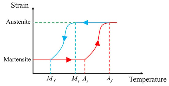
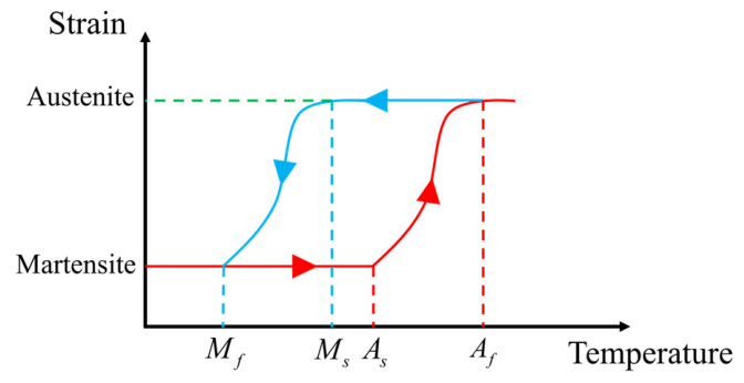
An SMA is a kind of phase change material that modifies its shape with temperature variations [22], including Cu alloys (such as Cu–Zn, Cu–Sn), Ni alloys (such as Ni–Al and Ni–Ti), and Fe alloys (such as Fe–Pd and Fe–Pt) [23]. Based on their shape memory effect (SME) characteristics, SMAs can be categorized into three types: (1) one-way SME; (2) two-way SME; and (3) pseudoelastic or superelastic SMAs. In this research, we use a two-way SME SMA, which has two changeable phases: martensite and austenite. Martensite can remain stable at low temperatures, while austenite can remain stable at high temperatures. An SMA phase transition temperature diagram is shown in Figure 1. When the SMA component is heated from a low temperature to a high one, martensite starts changing to austenite at temperature As and finishes changing at temperature Af. When the SMA component is cooled from a high temperature to a low one, austenite starts changing into martensite at temperature Ms and finishes changing at temperature Mf. This characteristic helps to keep the SMA in a high-temperature form, which is highly suitable for our research. SMAs can be heated quickly via a large current [24]. Although frequency-selective surfaces (FSSs) using phase-change materials, such as VO2, graphene, and SMAs, have been widely proposed in the literature [25,26,27,28], they have a critical drawback; namely, the response time constant, which can be significantly long. The phase change will affect the conductivity of VO2 and graphene in terms of terahertz, while SMAs can be used in microwave bands; e.g., SMA antennae [29,30] and reconfigurable metasurfaces [31,32]. Therefore, we use PIN diodes to provide an immediate response and SMA components to ensure HSE.
Figure 1.
SMA phase transition temperature diagram.
The remainder of this paper is organized as follows: Section 2 describes the design and the equivalent circuit analysis of the proposed HSE–ESS solution. Section 3 is devoted to comparing and discussing the numerical and experimental results. Section 4 compares the results of this work with the state of the art and analyzes how the time delay between PIN diode failures and the SMA components change to high-temperature shape influence SE performance of whole ESS. Finally, our conclusions are provided.
2. Materials and Methods
All the design processes and numerical simulations in this study were carried out using the numerical solver CST Studio Suite (Dassault Systemes, Paris, France), with a tetrahedral type of mesh and a unit cell boundary.
2.1. ESS Design
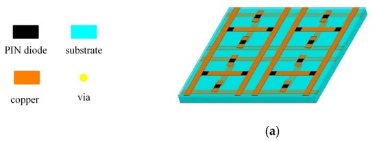
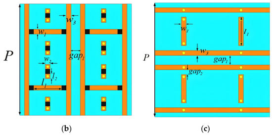
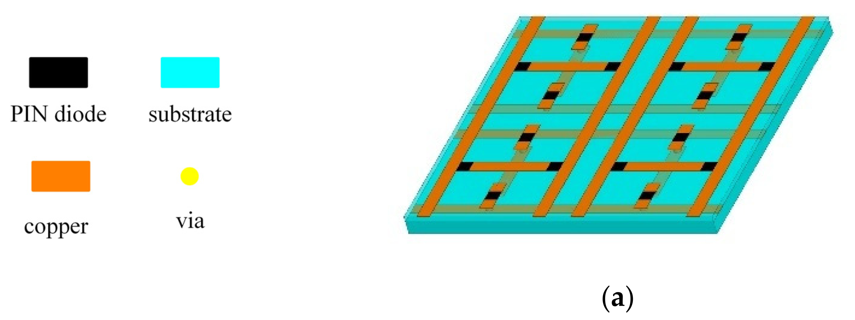
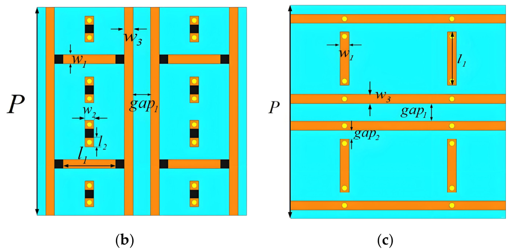
The ESS changes its working response between transmission and SE modes when the PIN diodes are turned “off” and “on”, respectively. The corresponding unit cell structures are shown in Figure 2, where an oblique view is shown in Figure 2a, containing 3 layers. The top and middle layer structures are the same but rotated 90°, with PIN diodes soldered on the top layer, as shown in Figure 2b and Figure 2c, respectively. The ESS is a series LC and PIN diode structure etched on different layers with polarization-independent switching capacity. The long copper lines enable parallel inductance. A standard 35 μm thick piece of copper was employed, returning to a FR-4 substrate, with relative dielectric constant and loss tangent of εr = 4.4 and tanδ = 0.02, respectively. The two substrate layers present in the design are of different thicknesses; i.e., h1 = 0.4 mm, and h2 = 1 mm. SMP1321-011LF PIN diodes (Skyworks Solutions Inc, Irvine, CA, USA) were employed. Two PIN diodes connected in series have their ends connected to a long strip of copper that can reach the boundary of the full ESS structure directly, such that they can be fed in parallel.
Figure 2.
Structure of the energy-selective surface (ESS): (a) oblique view, (b) top layer, and (c) middle layer. The parameters are as follows: p = 24 mm, l1 = 6 mm, l2 = 1 mm, w1 = 1 mm, w2 = 1 mm, w3 = 1 mm, h1 = 0.4 mm, h2 = 1 mm, gap1 = 2 mm, and gap2 = 1 mm.
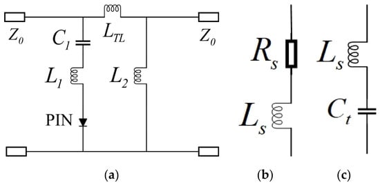
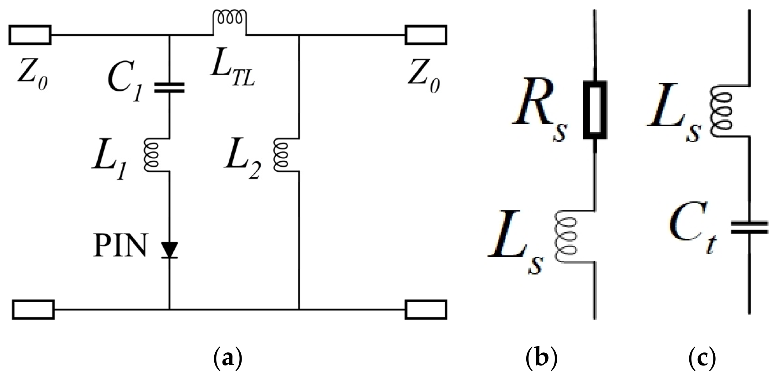
The geometric design is also analyzed through an equivalent circuit model (ECM), as shown in Figure 3a. ECMs have proven to be an effective means of analyzing metasurface structures. With regard to our design, the PIN diode includes a parasitic inductance Ls in series with a small resistor Rs in the “on” state and a parasitic inductor Ls in series with capacitor Ct in the “off” state, as shown in Figure 3b and Figure 3c, respectively.
Figure 3.
Equivalent circuit model (ECM): (a) ESS unit cell, (b) PIN diode in the “on” state, and (c) PIN diode in the “off” state. The parameters are as follows: L1 = 3.6 nH, L2 = 4.4 nH, C1 = 0.18 pF, Rs = 3 Ω, Ls = 1.5 nH, and Ct = 0.1 pF.
The inductance can be calculated approximately as follows [33]:
where l, w, and t are the length, width, and thickness of the metallic strip.
The capacitance can be calculated approximately as follows [34]:
where l and g are the length and distance of the metallic gap, ε0 is the vacuum dielectric constant, and εr is the relative dielectric constant of the substrate, leading to an average effective value of εeff = (εr+1)/2. Because there are 2 PIN diodes in 1 unit cell linked in series, the equivalent parameters are Ls_eff = 2Ls and Ct_eff = Ct/2. When the PIN diodes are in the “off” state, the admittance of the ESS unit cell is as follows:
By setting Yoff = 0, the transmission frequency foff can be obtained as
Conversely, when the PIN diodes are in the “on” state, the admittance of the ESS unit cell is
Similarly, by setting Yon = 0, the transmission frequency fon can be obtained as
By computing the values through the lumped parameters reported in the caption for Figure 3 and substituting them into (4) and (6), we obtain foff = 6.2 GHz and fon = 3.3 GHz. Because fon is far away from foff, it could be a reflection band for foff when the PIN diodes are “on”. Therefore, we use the “off” state of the PIN diodes as the transmission mode and the “on” state as the SE mode.
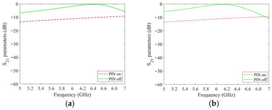
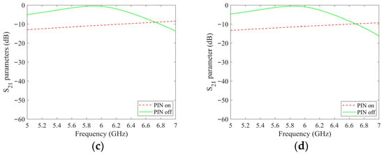
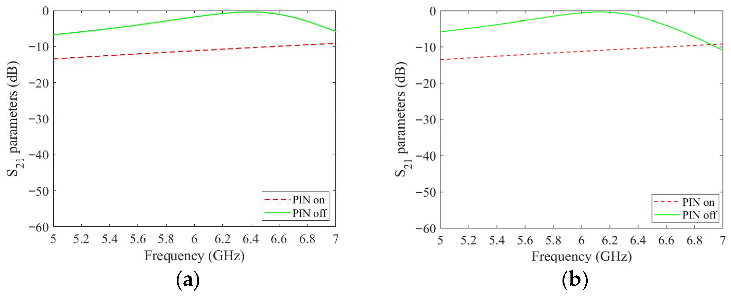
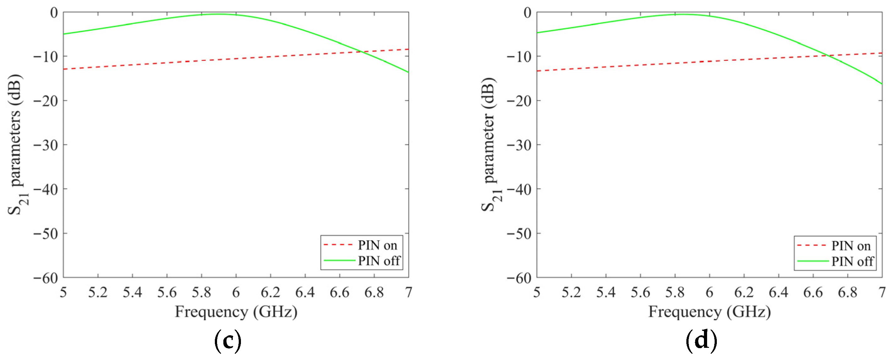
The simulation results for the ESS are shown in Figure 4, where Figure 4a,b pertain to TE polarization, while Figure 4c,d refer to TM polarization. Comparing the operating mode of the PIN diodes in the perpendicular direction with respect to a certain polarization reveals that they do not have an impact and, so, the response is independently controllable in terms of polarization. Furthermore, when the PIN diodes are “off”, the transmission frequency center is 6.3 GHz with a −3 dB transmission band from 5.78 to 6.79 GHz for TE polarization, whereas it is 5.9 GHz with a −3 dB transmission band from 5.34 to 6.29 GHz for TM polarization with a low IL. Conversely, when the PIN diodes are “on”, a −10 dB SE at the corresponding transmission band can be observed.
Figure 4.
S21 parameter simulation results for the ESS: (a) TE results when the PIN diodes in the y direction are “on”; (b) TE results when the PIN diodes in the y direction are “off”; (c) TM results when the PIN diodes in the x direction are “on”; and (d) TM results when the PIN diodes in the x direction are “off”.
2.2. HSE Design
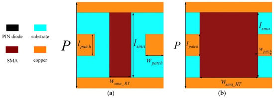
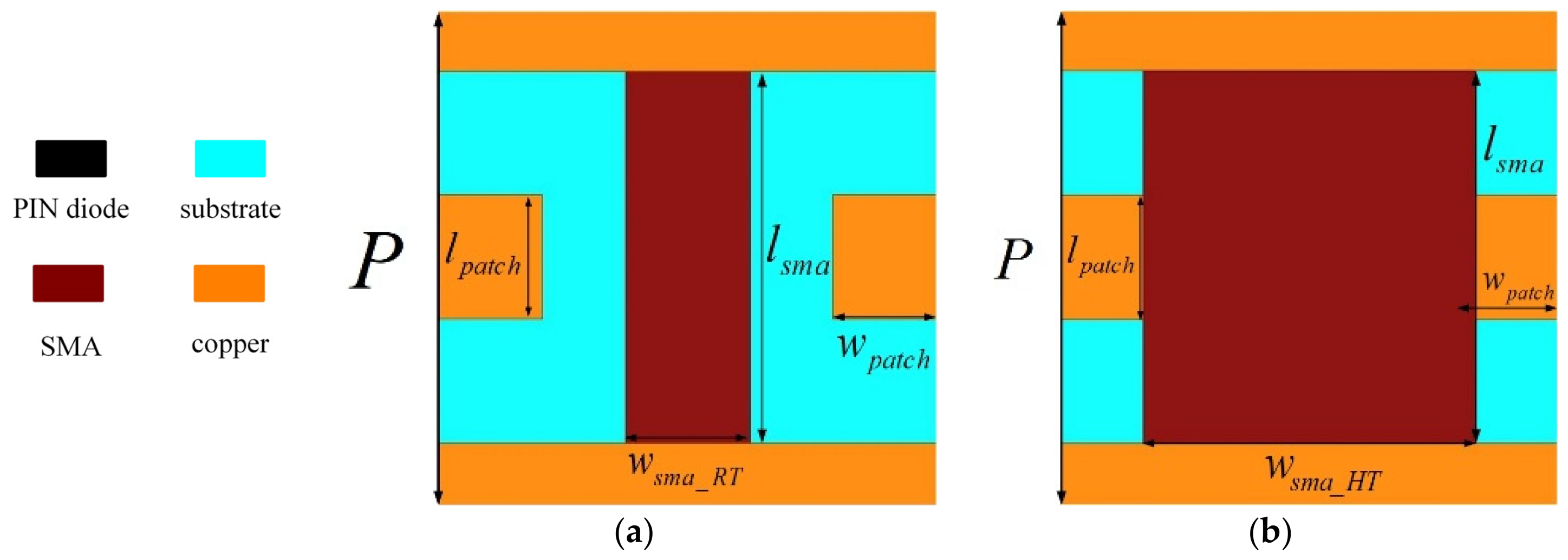
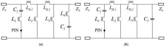
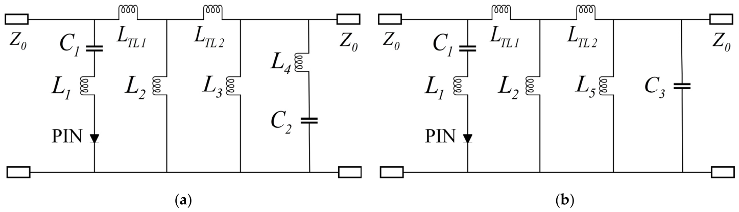
As mentioned earlier, the main aim of this study is to introduce an SMA in order to maintain the SE of the ESS, even in the event of PIN diode failure. Thus, we added SMA components to the bottom of the ESS, as shown in Figure 5. However, since SMA components require a certain (although limited) amount of time to change shape, we also need the PIN diodes in the HSE-ESS to respond immediately before they fail. In the simulation, we designed the SMA to have different widths, corresponding to different temperatures. Specifically, when SMA components function at low temperatures, they assume a narrow shape, and their width is denoted as wSMA_RT. Correspondingly, when SMA components operate at high temperatures, they have a wider area, and this width is denoted as wSMA_HT. Figure 5a portrays the SMA components’ behavior when operating at room temperature, while Figure 5b depicts the SMA components as a wide strip touching the patch when they are subjected to high temperatures. When the SMA components operate at high temperatures, the bottom side of the ESS is near the metal ground, which can be used for the HSE mode. When the SMA components operate at room temperature, they are in the transmission mode. To demonstrate the influence of transmission resonance caused by adding SMA components, Figure 6 shows the ECMs of SMA components working at room temperature and PIN diodes in the “off” state, while TE polarization is shown in Figure 6a and TM polarization is shown in Figure 6b.
Figure 5.
Bottom-side structures of the ESS: (a) SMA operating at room temperature and (b) SMA operating at high temperatures. The parameters are as follows: lSMA = 16 mm, wSMA_RT = 6 mm, wSMA_HT = 16 mm, lpatch = 8 mm, and wpatch = 6 mm.
Figure 6.
ECMs of SMA components working at room temperature: (a) TE polarization and (b) TM polarization. The parameters are as follows: L3 = 7.6 nH, L4 = 4.2 nH, L5 = 7.2 nH, C2 = 5 fF, and C3 = 0.06 pF.
For TE polarization, the total admittance of the HSE–ESS unit cell can be expressed as follows:
where m1 = C1 + Ct_eff, m2 = −C1Ct_eff(L1 + Ls_eff + L2 + LTL1), m3 = −(L3 + L4)C2, n1 = L2 + LTL1, n2 = C1 + Ct_eff, n3 = −C1Ct_eff(L1 + Ls_eff), n4 = L3 + LTL2, n5 = −C2(L3LTL2 + L4LTL2 + L3L4), a1 = m2n5 + n1n2m3, c1 = m1n4 + n1n2, and b1 = m1n5 + m2n4 + n1n3 + n1n2m3.
By setting YTE = 0, we can obtain two transmission frequencies, fTE1 and fTE2 as follows:
Conversely, for TM polarization, the total admittance of the HSE–ESS unit cell can be expressed as follows:
where m4 = −L5C3, n6 = L5 + LTL2, n7 = −L5LTL2C2, a2 = m2n7 + n1n2m4, b2 = m1n7 + m2n6 + n1n3 + n1n2m4, and c2 = m1n6 + n1n2.
By setting YTM = 0, we can obtain two transmission frequencies, fTM1 and fTM2, as follows:
By computing the values via the lumped parameters reported in the caption for Figure 6, we obtain fTE1 = 7.3 GHz, fTE2 = 27.2 GHz, fTM1 = 6.6 GHz, and fTM2 = 14.9 GHz. In comparison to the transmission centers shown in Figure 4, fTE1 and fTM1 are near the transmission centers of TE and TM polarization, respectively, which can still be used as a transmission mode.
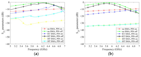
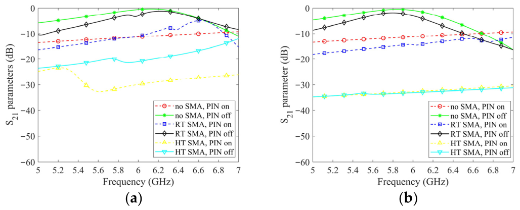
In order to clearly and explicitly demonstrate the influence of SMA, we compare the S21 parameters through numerical simulations in three different configurations: no SMA, SMA components working at room temperature, and SMA components working at high temperatures (Figure 7). Because the operating state of vertical PIN diodes has no influence as in this case, we only show the simulation results for vertical PIN diodes in the “off” state. The six operating states of PIN diodes and SMA components are as follows. (1) Transmission mode: PIN diodes are in the “off” state, and no SMA or SMA components are operating at room temperature. (2) SE mode: The PIN diodes are in the “on” state, and no SMA or SMA components are operating at room temperature. (3) HSE mode: SMA components are operating at high temperatures, and PIN diodes are in failure mode. Figure 7a shows that the −3 dB transmission band is 5.85–6.48 GHz, while the transmission center is 6.22 GHz with 1.2 dB IL for TE polarization. The SE level is nearly 30 dB. Figure 7b shows that the −3 dB transmission band is 5.59–5.98 GHz, while the transmission center is 5.8 GHz with 1.9 dB IL for TE polarization. The SE level is more than 30 dB. Comparing the transmission modes reveals that adding SMA components will add about 1 dB IL, and the transmission bandwidth will become slightly narrower. By comparing the SE and HSE modes, we can observe that adding SMA components improves the SE by about 20 dB. Furthermore, regarding the HSE mode, we can observe that the HSE-ESS will maintain SE for both TE and TM polarization, regardless of whether the PIN diodes are active, ensuring the desired HSE protection. Comparing the ECM analysis and simulation results, we can observe that the ECM analysis of the ESS unit cell is more correct than that for the HSE–ESS unit cell. ECM analysis requires the dimensions of the unit cell to be significantly smaller than the wavelength. The dimensions of the proposed HSE–ESS unit cell are twice those of the ESS unit cell, which is not small enough with respect to the expectations for ECM analysis. This weakens the quasi-static hypothesis, leading to the difference between the ECM analysis and simulation results.
Figure 7.
S21 parameter simulation results regarding the HSE–ESS: (a) TE polarization and (b) TM polarization. RT: room temperature, HT: high temperature.
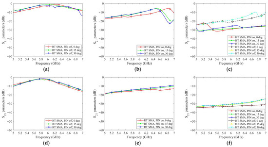
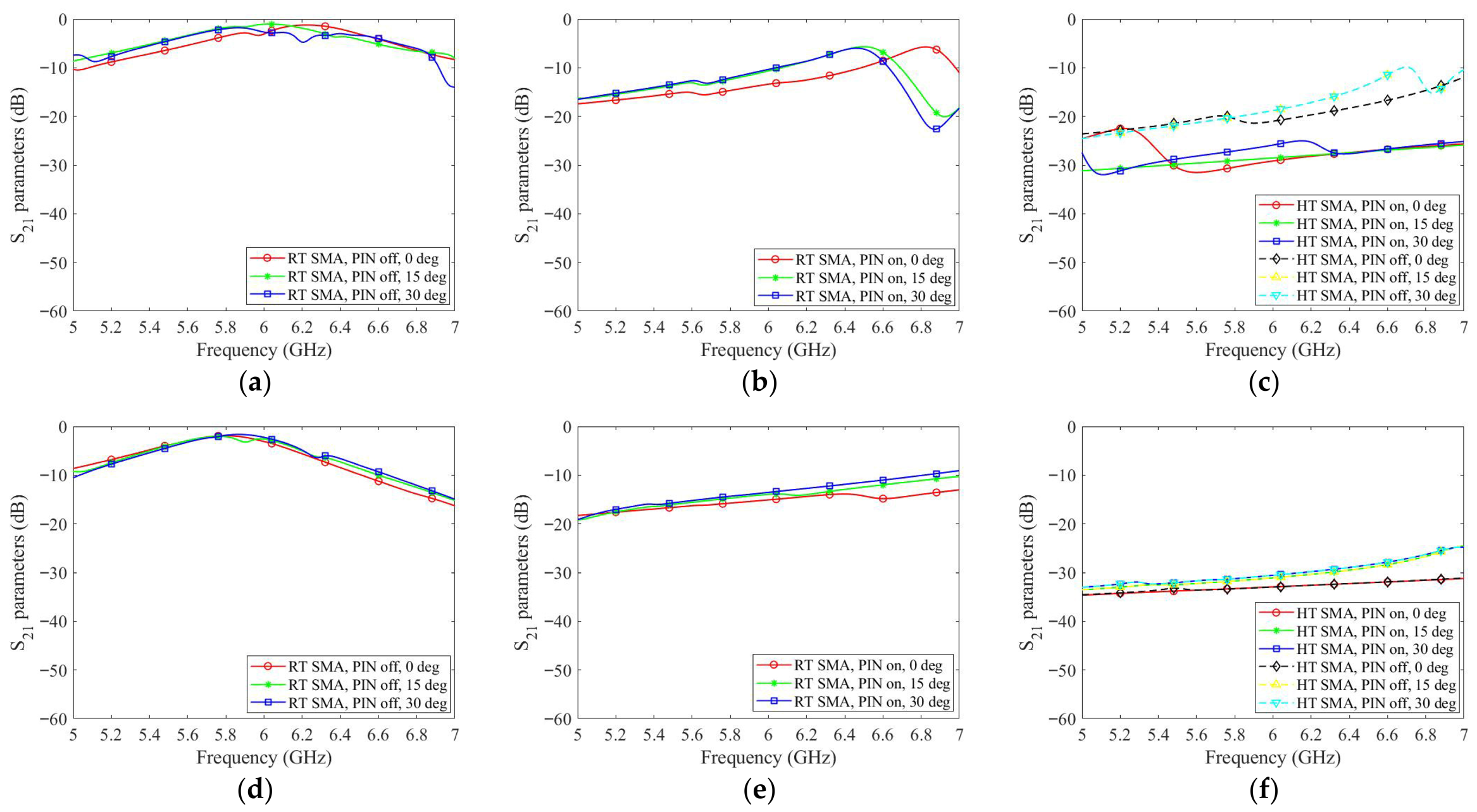
The transmission, SE, and HSE modes of TE polarization are shown in Figure 8a, Figure 8b, and Figure 8c, respectively, while the different working modes of TM polarization are shown in Figure 8d–f. We can observe that the angle stability is 30°. The incident angle has very little influence, especially for TM polarization.
Figure 8.
Angle stability of the HSE–ESS: (a) Transmission mode of TE polarization; (b) SE mode of TE polarization; (c) HSE mode of TE polarization; (d) transmission mode of TM polarization; (e) SE mode of TM polarization; and (f) HSE mode of TM polarization.
2.3. Automatic Heating Circuit
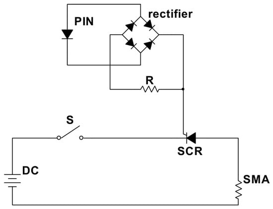
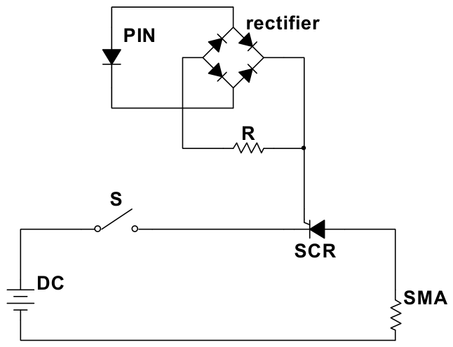
SMA components need to be heated automatically when the HSE–ESS is affected by incident HPMs. The automatic heating circuit includes PIN diodes in the lossy layer and is linked to the SMA components in the bottom layer of the ESS metasurface. We use PIN diodes as sensors and a silicon-controlled rectifier (SCR) as the switching component of the automatic heating circuit, as shown in Figure 9. An SCR is a special kind of electronic switch with 1 control port and 2 load ports. When high voltage is applied to the control port of the SCR, the SCR’s 2 load ports will connect and keep connecting, regardless of whether the control port remains active. Once the SCR is active, it can only be turned off when the load path changes to open-road. Therefore, even if the PIN diodes are burnt, the heating path for SMA components will not be influenced. The mechanical switch is normally closed. Therefore, when HPM beams are incident to the HSE–FSR, the circuit works automatically: (i) the HPMs polarize the PIN diodes and generate current for the rectifier; (ii) the rectifier outputs direct current (DC) to the SCR’s control port; (iii) electricity from the DC source is conducted to the SMA components, and heating continues; (iv) the mechanical switch is turned off when the SMA components no longer need to be heated; (v) finally, the mechanical switch is turned on to reset the circuit, and the PIN diodes—which might be burnt–are replaced for the next time the circuit will be used.
Figure 9.
Automatic heating circuit for the SMA.
3. Experimental Results
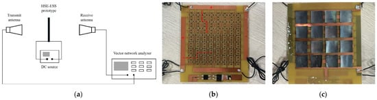
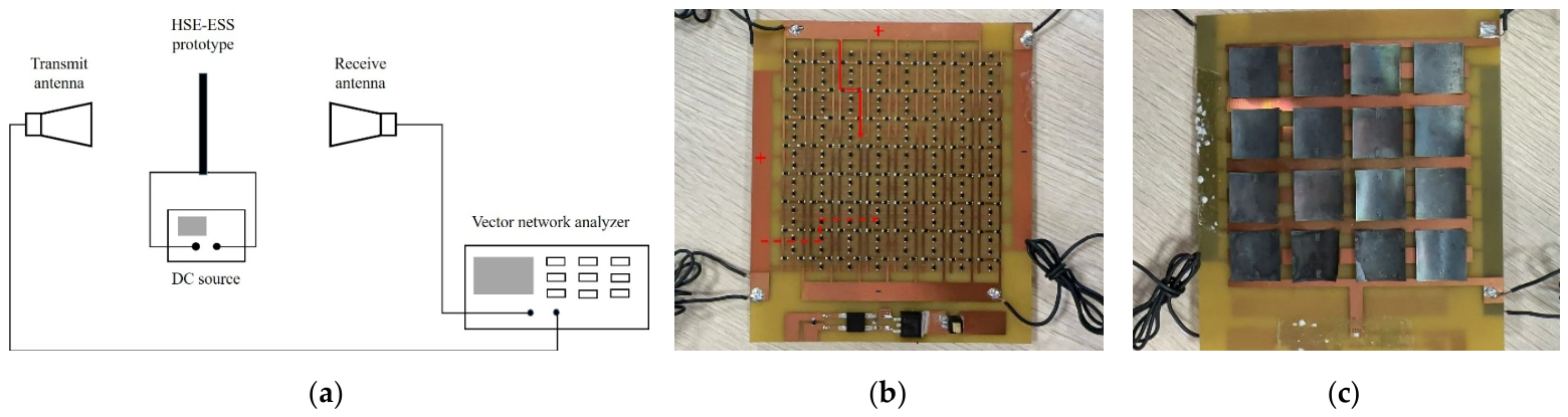
We fabricated a prototype comprising a 10 × 10 array through printed circuit board technology, as shown in Figure 10. The overall dimensions are 120 mm × 137.5 mm × 1.4 mm. According to the design process, the top and middle layers were etched on 0.4 mm and 1 mm thick FR-4 substrates, respectively. All the lumped components were inserted into the prototype via surface-mounting technology, while the SMA components were soldered onto the bottom layer copper via laser welding. The selected SMA is a type of NiTi alloy that undergoes high-temperature deformation at approximately 60 °C to 80 °C. Because all the PIN diodes are connected in parallel, extra bias wires are not necessary. Since the HSE–ESS does not have an absorptive feature, we only measured the transmission S21 parameter using standard free-space measurement technology. Here, DC voltage was used to simulate the situation where HPMs polarize the PIN diodes. In particular, we adopted horn antennas (operating between 2 GHz and 18 GHz (Schwarzbeck)) connected to a Vector Network Analyzer (N5245A (Agilent, Santa Clara, CA, USA)). The distance from the antennas to the HSE–ESS panel was fixed at 1.5 m, thus ensuring the far-field condition for the employed horn antennas.
Figure 10.
Fabricated HSE-ESS prototype: (a) measurement schematic; (b) feeding mode of the top layer (solid line) and middle layer (dotted line); and (c) SMA components of the bottom layer.
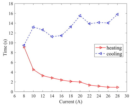
We used a constant-current source to evaluate the relationship between the deformation time of the SMA components and the current magnitude, as shown in Figure 11. As depicted, the SMA components change their shape faster when a larger heating current is applied, up until the deformation time is less than 1 s. Conversely, the cooling time increases when the SMA components are heated to high temperatures via a higher heating current. This is because there is more heat energy in SMA components under a higher heating current.
Figure 11.
Relationship between deformation time and current.
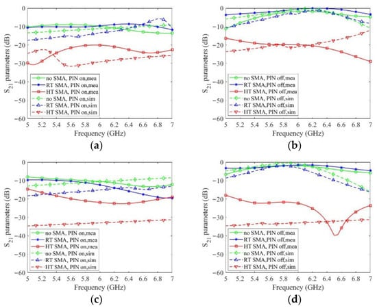
The comparisons between the measured and simulation results are shown in Figure 12. In order to demonstrate the effect of adding SMA components, we compare situations without an SMA, with SMA components operating at room temperature, and with SMA components operating at high temperatures under the same polarization and with the same operating state of the PIN diodes. Figure 12a,b show that the experimental results exhibit good agreement with the simulation for TE polarization. Conversely, Figure 12c,d show that the SE levels in the measured results for the high-temperature SMA are worse than those in the simulation for TM polarization. This phenomenon is the result of the lack of an absorption frame outside the HSE–ESS sample during measurement. Therefore, scattering and diffraction both occur at the edge of the finitely large sample, leading to a higher transmission coefficient. Furthermore, the SMA samples were arc-shaped at room temperature, which is unlike the simulation setting, where everything is perfectly planar, which may also explain the discrepancies. All the experimental results show that adding SMA components can significantly improve the SE of ESSs. Reasonably adjusting the structure of the SMA layer can provide a universal method for turning an ESS into an HSE–ESS.
Figure 12.
Comparisons between the measured and simulation-sourced results: (a) TE polarization when the PIN diodes are in the “on” state; (b) TE polarization when the PIN diodes are in the “off” state; (c) TM polarization when the PIN diodes are in the “on” state; and (d) TM polarization when the PIN diodes are in the “off” state.
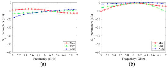
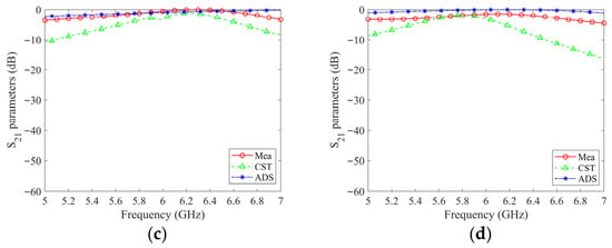
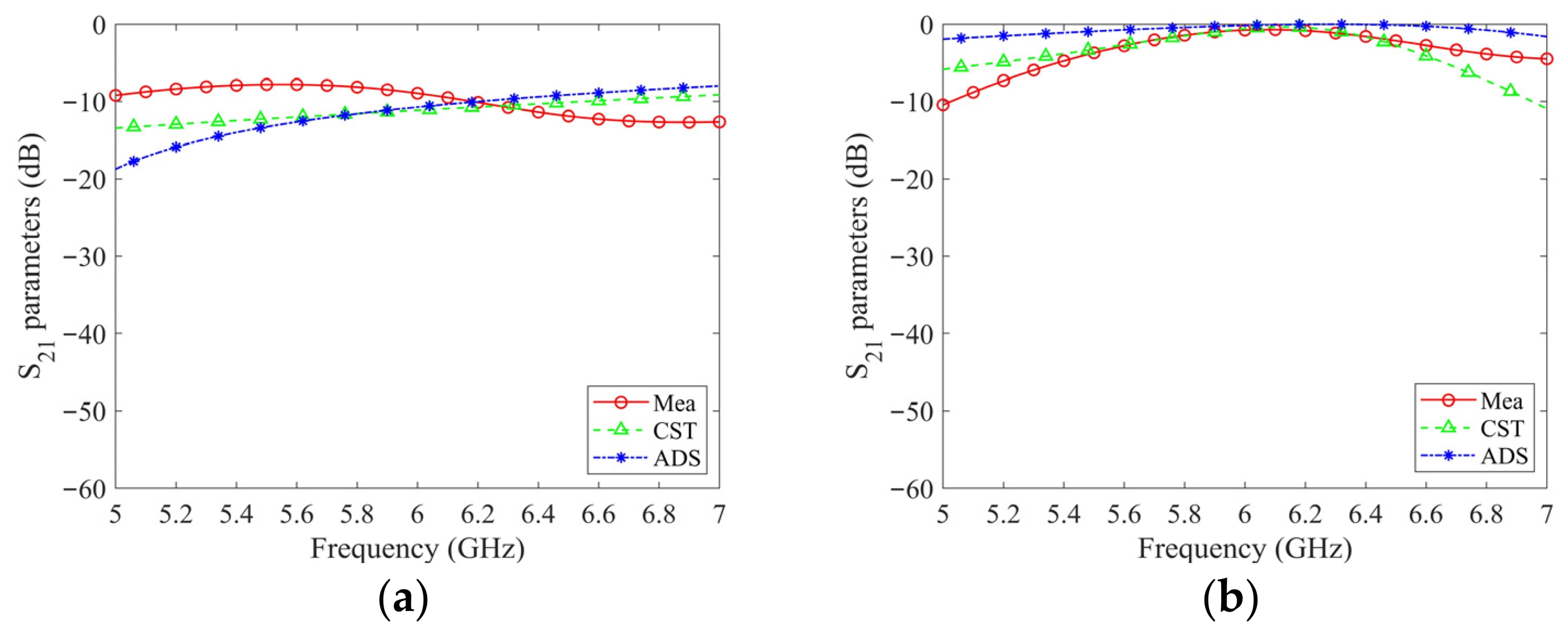
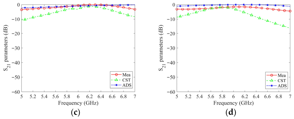
Furthermore, we ran an advanced design system (ADS) simulation based on ECM analysis and compared the measurement, CST, and ADS results, as shown in Figure 13. Figure 13a,b compare the results obtained for PIN diodes operating in the “on” and “off” states, respectively, without SMA components, while (c) and (d) show TE and TM polarization, respectively, when the PIN diodes are “off” and the SMA components are operating at room temperature. The results of the comparison verified those from the ECM analysis.
Figure 13.
Comparison of the measurement, CST, and ADS results: (a) PIN diodes in the “on” state without SMA components, (b) PIN diodes in the “off” state without SMA components, (c) PIN diodes in the “off” state with SMA components operating at room temperature for TE polarization, and (d) PIN diodes in the “off” state with SMA components operating at room temperature for TM polarization.
4. Discussion
The simulation performances for our ESS and relevant state-of-the-art ESSs with respect to HPM protection are compared in Table 1. SE levels, including for the whole working band and the maximum, are provided. The whole-working-band SE level achieved in this work is higher than in others, due to the addition of SMA components. Furthermore, the proposed design maintains its unique HPM protection capacity even when the PIN diodes eventually fail. Combining high SE, an independently switchable polarization capacity, and reliability even when PIN diodes fail, the proposed design represents a competitive solution in harsh EM environments. Therefore, adding SMA components may become a universal method for enhancing the SE and reliability of ESSs in the future.
Table 1.
Simulation performance comparison.
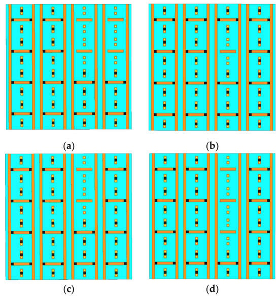
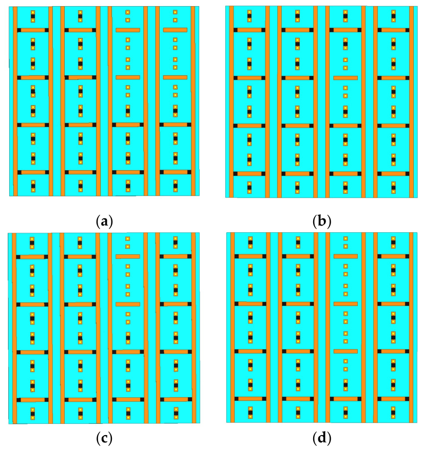
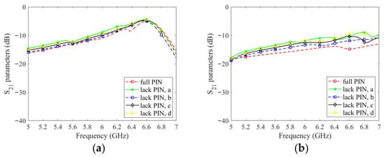
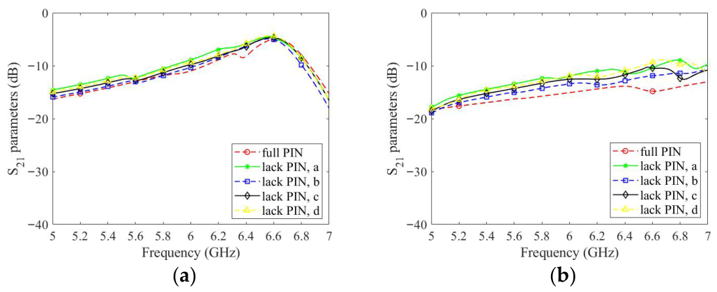
Furthermore, we ran several simulations of removing some PIN diodes from the HSE–ESS structure with SMA components operating at room temperature, in order to analyze the influence of the time delay on the transition of the SMA components. In the simulations, we combined four unit cells together into one big unit cell and then removed some PIN diodes, as shown in Figure 14, which depicts the following situations: (a) removing all PIN diodes from one basic unit cell; (b) removing all PIN diodes from 1/4 basic unit cell; (c) removing 1/2 PIN diodes from one basic unit cell; and (d) removing all PIN diodes from 1/2 basic unit cell and an adjacent 1/4 basic unit cell. The simulation results are shown in Figure 15, where a, b, c, and d correspond to Figure 14a, Figure 14b, Figure 14c, and Figure 14d, respectively. As shown, the ESS can still maintain SE even when some PIN diodes are burnt, providing more time for the SMA components to change shape and improve the SE performance. Although the ESS can still maintain SE when only a small number of PIN diodes are burnt, the burning out of PIN diodes due to HPMs is unpredictable, especially for prolonged HPM emission, which is highly likely to burn all PIN diodes. The ESS requires most of the PIN diodes to avoid being burnt during the entire duration of HPM emission. Research on burning PIN diodes using a high-power source, accounting for repetition frequency (20 Hz) and peak power (2 kw), has been reported in [21], which indicated that burning the I layer of PIN diodes requires 20 pulses (in 1 s). Another measurement used 157 pulses (in 1.57 s) to burn PIN diodes, using a high-power source with a repetition frequency of 100 Hz and high voltage (280 V) [35]. With a large enough current and thin enough SMA component dimensions [22], SMA components can finish the transition before the PIN diodes fail. In other words, the influence of the time delay on the SMA components’ transition can be reduced by using a large enough current and thinner SMA components. This reduces the duration for which PIN diodes must be spared from being burnt from the entirety of HPM emission to a short period, significantly enhancing the reliability of ESSs, especially when continuous HPM emission occurs.
Figure 14.
Simulation settings regarding the removal of some PIN diodes: (a) removing all PIN diodes of 1 basic unit cell; (b) removing all PIN diodes of 1/4 basic unit cell; (c) removing all PIN diodes of 1/2 basic unit cell in 1 series; and (d) removing all PIN diodes of 1/2 basic unit–cell and adjacent 1/4 basic unit cell in a series.
Figure 15.
Simulation results regarding the removal of some PIN diodes: (a) TE polarization and (b) TM polarization.
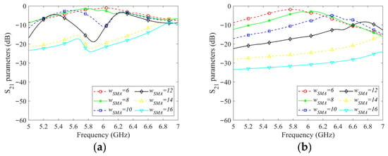
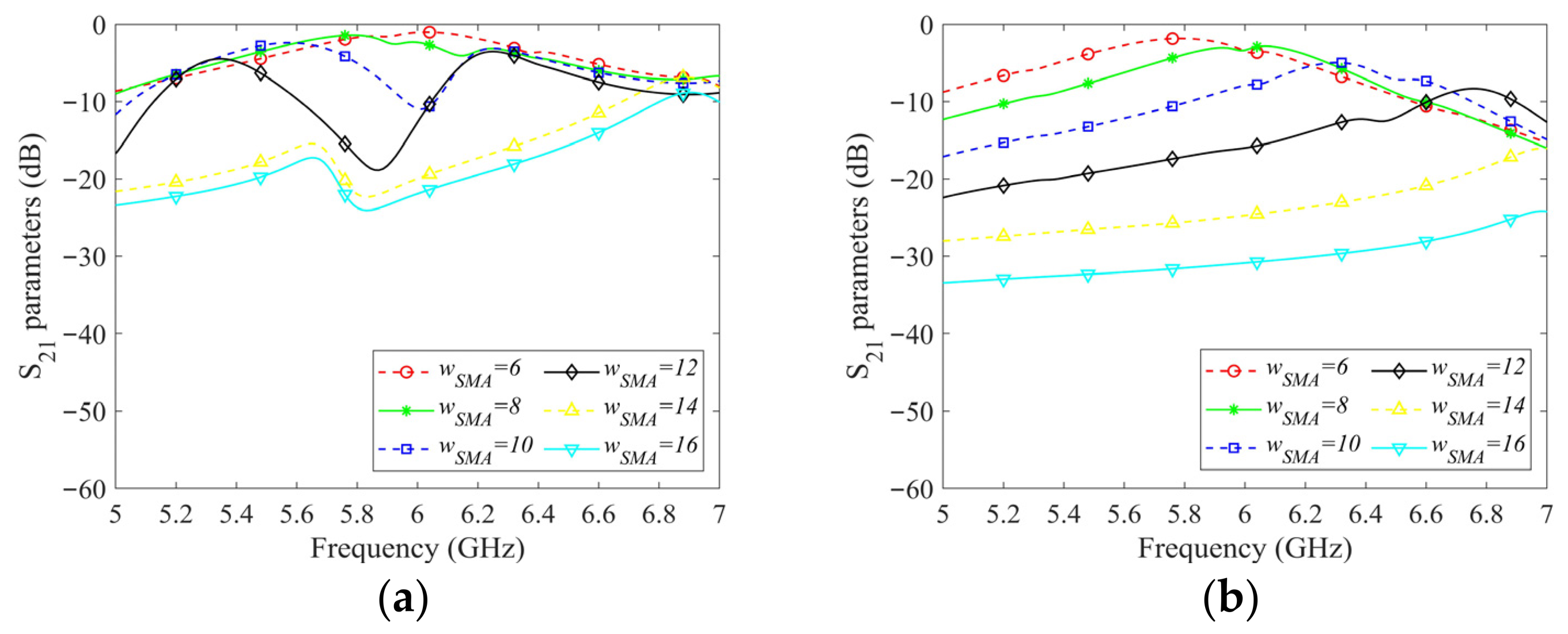
Furthermore, to analyze the influence of the deformation of the SMA components, we ran simulations of the HSE-ESS unit cell with different widths of SMA components with PIN diodes in the “off” state, as shown in Figure 16. Figure 16a shows the simulation results for TE polarization, while Figure 16b shows those for TM polarization. Evidently, the SE is higher with wider SMA components. Until wSMA = 14 mm or even later, corresponding to the moment the SMA components make contact with the copper patch, the HSE–ESS is in HSE mode. Therefore, the key point of HSE is that the SMA components must touch the copper patch; additionally, when the SMA components cover a greater area, the SE will be higher.
Figure 16.
Simulation results for the HSE-ESS with SMA components with different widths with PIN diodes in the “off” state.
Furthermore, according to our method of fabricating SMA components, the demission of SMA is already the smallest with a change in shape in only one direction. This causes different responses to TE and TM polarization. If SMA components can be made smaller or reshaped both horizontally and vertically, the responses to TE and TM polarization will be more similar. With the development of SMA fabrication technology, the HSE-ESS’s performance can be expected to improve further.
5. Conclusions
In this paper, we proposed a novel HSE-ESS with independently switching polarization capacity including SMA components for high-power performance preservation. In particular, the SMA components can be used as a back-up for the PIN diodes when a high current leads to their failure. We performed accurate numerical simulations and acquired experimental measurements from fabricated prototypes, confirming their excellent HSE protection capabilities. The results indicate that adding SMA components can be a valuable and universal method for turning an ESS into an HSE-ESS. Furthermore, the reliability requirement for PIN diodes is also reduced, which enhances the reliability of ESSs.
Based on the measured heating and cooling times of the SMA components, a more intelligent heating circuit to control the temperature of SMA components should be developed in the future. This intelligent heating circuit will need to use a high current to quickly heat the SMA components (i.e., within 1 s) and a small circuit to retain shape at high temperatures, thus avoiding long cooling times. Although the SMA components can sustain hundreds of heating–cooling cycles, the tolerance of PIN diodes may not be so high. If too many PIN diodes are burnt by multiple HPM strikes, the proposed HSE–ESS will no longer provide automatic protection against HPMs. However, we can still use a heating circuit to heat the SMA components and ensure HPM protection if more HPM strikes are expected to happen later. A more reliable approach would be to replace the damaged PIN diodes after encountering HPM strikes, if possible. No matter how badly the PIN diodes are damaged, the HSE–ESS can maintain SE performance, with the SMAs serving as a back-up.
Furthermore, based on width analysis of the SMA components, we may obtain higher SE levels if we fabricate SMA components with larger dimensions. By more reasonably designing the shape of the SMA components and unit cell structures, we can further enhance the SE of HSE–ESSs and their protection from extreme HPM strikes.
Author Contributions
Conceptualization, A.M. and Z.L.; methodology, W.L.; software, Z.L.; validation, H.Y.; resources, W.L.; formal analysis, Z.L.; data curation, Z.L. and H.Y.; writing—original draft preparation, Z.L.; writing—review and editing, D.B.; visualization, Z.L.; supervision, W.L. and A.M. All authors have read and agreed to the published version of the manuscript.
Funding
This research received no external funding.
Institutional Review Board Statement
Not applicable.
Informed Consent Statement
Not applicable.
Data Availability Statement
The original contributions presented in this study are included in the article.
Conflicts of Interest
The authors declare no conflicts of interest.
Abbreviations
The following abbreviations are used in this manuscript:
| HPM | High-Power Microwave |
| ESS | Energy-Selective Surface |
| IL | Insertion Loss |
| SE | Shielding Effectiveness |
| SMA SME | Shape Memory Alloy Shape Memory Effect |
| HSE | High Shielding Effectiveness |
| HSE–ESS | High-Shielding-Effectiveness Energy-selective Surface |
| FSS | Frequency-Selective Surface |
| ECM | Equivalent Circuit Model |
| SCR | Silicon-Controlled Rectifier |
| DC | Direct Current |
References
- Eleftheriades, G.V. Protecting the weak from the strong. Nature 2014, 505, 490–491. [Google Scholar] [CrossRef] [Scilit]
- Benford, J.; Swegle, J.A.; Schamiloglu, E. High Power Microwaves; IEEE: New York, NY, USA, 2007. [Google Scholar]
- Huang, Z.; Zhang, Y.; Ge, X. Damage Effects and Protection on Low-Noise Amplifiers Under High-Power Microwaves. IEEE Trans. Electromagn. Compat. 2025, 67, 842–853. [Google Scholar] [CrossRef] [Scilit]
- Mao, Q.; Xiang, Z.; Huang, L.; Meng, J.; Wang, H.; Yang, C.; Cui, Y. High-Power Microwave Pulse-Induced Failure on Unmanned Aerial Vehicle System. IEEE Trans. Plasma Sci. 2023, 51, 1885–1893. [Google Scholar] [CrossRef] [Scilit]
- Liang, Q.-S.; Chai, C.-C.; Wu, H.; Liu, Y.-Q.; Li, F.-X.; Yang, Y.-T. Mechanism Analysis and Thermal Damage Prediction of High-Power Microwave Radiated CMOS Circuits. IEEE Trans. Device Mater. Reliab. 2021, 21, 444–451. [Google Scholar] [CrossRef] [Scilit]
- Yang, C.; Liu, P.-G.; Huang, X.-J. A Novel Method of Energy Selective Surface for Adaptive HPM/EMP Protection. IEEE Antennas Wirel. Propag. Lett. 2013, 12, 112–115. [Google Scholar] [CrossRef] [Scilit]
- Yang, G.H.; Yang, X.; Zhang, K.; Wang, Y.; Zhang, T. An L-band narrowband energy selective surface design. In Proceedings of the 2019 Cross Strait Quad-Regional Radio Science and Wireless Technology Conference (CSQRWC), Taiyuan, China, 18–21 July 2019. [Google Scholar]
- Ning, H.; Ke, W.; Jihong, Z.; Song, Z.; Zhaofeng, W.; Chenxi, L.; Peiguo, L. Design of Ultrawideband Energy-Selective Surface for High-Power Microwave Protection. IEEE Antennas Wirel. Propag. Lett. 2019, 18, 669–673. [Google Scholar] [CrossRef] [Scilit]
- Wang, X.; Deng, L.; Chen, L.; Qu, M.; Liu, X.; Chen, W. An S-Band Dual-Polarization Energy Selective Surface with Low-Cost Design. In Proceedings of the 2023 International Applied Computational Electromagnetics Society Symposium (ACES-China), Hangzhou, China, 15–18 August 2023; pp. 1–3. [Google Scholar]
- Shangyu, L.; Guohui, Y.; Kuang, Z.; Yingsong, L. Surface Simulation and Design of C-band Energy Selective Surface. In Proceedings of the 2022 International Applied Computational Electromagnetics Society Symposium (ACES-China), Xuzhou, China, 9–12 December 2022; pp. 1–4. [Google Scholar]
- Wu, Z.; Liu, P.; Deng, B.; Tian, T.; Zha, S.; Ni, X. An Ultrabroadband Energy Selective Surface with Nonreciprocal Performance for HIRF Protection. IEEE Trans. Electromagn. Compat. 2023, 65, 1202–1210. [Google Scholar] [CrossRef] [Scilit]
- Tian, T.; Huang, X.; Xu, Y.; Liu, P.; Liu, C.; Hu, N.; Zhang, J.; Wu, Z. A Wideband Energy Selective Surface with Quasi-Elliptic Bandpass Response and High-Power Microwave Shielding. IEEE Trans. Electromagn. Compat. 2024, 66, 224–233. [Google Scholar] [CrossRef] [Scilit]
- Xia, R.; Ren, J.; Xue, Z. A Tunable Ultra-Broadband Energy Selective Surface Design. In Proceedings of the 2024 IEEE 7th Information Technology, Networking, Electronic and Automation Control Conference (ITNEC), Chongqing, China, 20–22 September 2024; pp. 931–935. [Google Scholar]
- Zhang, J.; Kang, F.; Liu, Z.; Qu, Z.; Xu, M.; Zha, S.; Liu, P. Design of Ultrawideband Energy-Selective Surface Based on Triple-Layer Structure and Semiconductor for HIRF Prevention. IEEE Trans. Antennas Propag. 2025, 73, 9619–9624. [Google Scholar] [CrossRef] [Scilit]
- Zhong, S.; Chen, M.; Xu, G.; Chen, Y. Dual-Band Energy-Selective Surface with Enhanced Independence Based on Two-Layer Diode-Loaded FSS. IEEE Trans. Antennas Propag. 2024, 72, 5011–5020. [Google Scholar] [CrossRef] [Scilit]
- Liu, X.; Chen, X.; Han, L.; Su, J.; Ma, R.; Zhang, W. Dual-Band Energy-Selective Surface with Wide Absorption Band. IEEE Trans. Microw. Theory Tech. 2025, 73, 10241–10249. [Google Scholar] [CrossRef] [Scilit]
- Du, Y.; Zhang, Y.; Yu, W.; Luo, G.Q. Design of Dual-Band Energy Selective Surface Based on Diode-Loaded LC Resonators. In Proceedings of the 2025 18th IEEE United Conference on Millimeter Waves and Terahertz Technologies (UCMMT), Nanjing, China, 25–28 August 2025. [Google Scholar]
- Wang, X.; Zhou, D.; Yang, L.; Liu, Q.; Wang, Z.; Xu, H. A Novel Energy-Selective Surface with a Covert Passband for High-Power Microwave Protection. IEEE Trans. Antennas Propag. 2026, 74, 1138–1143. [Google Scholar] [CrossRef] [Scilit]
- Ning, H.; Yuting, Z.; Jihong, Z.; Peiguo, L.; Hui, X.; Filippo, C. High-Performance Energy Selective Surface Based on Equivalent Circuit Design Approach. IEEE Trans. Antennas Propag. 2022, 70, 4526–4538. [Google Scholar] [CrossRef] [Scilit]
- Li, C.; Zhang, T.; Bao, H.; Ding, D. Design of a Broadband Energy-Selective Surface with Ultrahigh Shielding Efficiency. IEEE Antennas Wirel. Propag. Lett. 2024, 23, 4303–4307. [Google Scholar] [CrossRef] [Scilit]
- Zhao, J.; Chen, Q.; Zhao, G.; Chen, C.; Chen, Z. Damage accumulation mechanism in PIN diode limiters induced via multiple microwave pulses. Sci. Rep. 2020, 10, 1709. [Google Scholar] [CrossRef] [Scilit]
- Yuan, H.; Fauroux, J.C.; Chapelle, F.; Balandraud, X. A review of rotary actuators based on shape memory alloys. J. Intell. Mater. Syst. Struct. 2017, 28, 1863–1885. [Google Scholar] [CrossRef] [Scilit]
- Barbarino, S.; Saavedra Flores, E.I.; Ajaj, R.M.; Dayyani, I.; Friswell, M.I. A review on shape memory alloys with applications to morphing aircraft. Smart Mater. Struct. 2014, 23, 063001. [Google Scholar] [CrossRef] [Scilit]
- Velázquez, R.; Pissaloux, E.E. Modelling and temperature control of shape memory alloys with fast electrical heating. Int. J. Mech. Control 2012, 13, 3–10. [Google Scholar]
- Scott, S.; Nordquist, C.D.; Cich, M.J.; Jordan, T.S.; Rodenbeck, C.T. A frequency selective surface with integrated limiter for receiver protection. In Proceedings of the Antennas and Propagation Society International Symposium (APSURSI), Chicago, IL, USA, 10 November 2012; IEEE: New York, NY, USA, 2012; pp. 1–2. [Google Scholar]
- Xu, G.; Li, Q.; Su, H.; Huang, H.; Wang, S. VO2-Based metasurface for dynamically tunable terahertz surface plasmonic waves. Mater. Res. Express 2024, 11, 075801. [Google Scholar] [CrossRef] [Scilit]
- Nguyen, P.T.H.; Nguyen, Q.H.; Huynh, S.T.; Mai, T.H.; Nguyen, T.T.; Bui, T.S.; Le, M.T.; La, D.D. Flexible Metamaterial Absorber in Paper Substrate using Graphene Conductive Ink for WiMAX Applications. J. Electron. Mater. 2025, 54, 3949–3956. [Google Scholar] [CrossRef] [Scilit]
- Park, E.; Lee, M.; Jeong, H.; Phon, R.; Kim, K.; Park, S.; Lim, S. 3-D/4-D-Printed Reconfigurable Metasurfaces for Controlling Electromagnetic Waves. Proc. IEEE 2024, 112, 1000–1032. [Google Scholar] [CrossRef] [Scilit]
- Kowalewski, J.; Mahler, T.; Reichardt, L.; Zwick, T. Shape Memory Alloy (SMA)-Based Pattern-Reconfigurable Antenna. IEEE Antennas Wirel. Propag. Lett. 2013, 12, 1598–1601. [Google Scholar] [CrossRef] [Scilit]
- Taoum, J.; Shammas, E.; Costantine, J. An Unconventional Shape Memory Alloy Low-Power Ratchet for Reconfiguring the Polarization of a Moiré Pattern-Based Antenna. IEEE Trans. Antennas Propag. 2022, 70, 10095–10103. [Google Scholar] [CrossRef] [Scilit]
- Lor, C.; Lim, S. Multi-functional anisotropic metasurface using mechanical shape memory alloy spring. In Proceedings of the 2022 13th International Conference on Information and Communication Technology Convergence (ICTC), Jeju Island, Republic of Korea, 19–21 October 2022; pp. 847–849. [Google Scholar]
- Zhang, K.; Ma, T.; Liu, J.; Tian, X.; Zhu, J.; Tan, C. Dynamically tunable and polarization-insensitive dual-band terahertz metamaterial absorber based on TiNi shape memory alloy films. Results Phys. 2021, 23, 104001. [Google Scholar] [CrossRef] [Scilit]
- Bahl, I.J.; Bhartia, P. Microwave Solid State Circuit Design; Wiley-Interscience: New York, NY, USA, 1989. [Google Scholar]
- Sarabandi, K.; Behdad, N. A Frequency Selective Surface with Miniaturized Elements. IEEE Trans. Antennas Propag. 2007, 55, 1239–1245. [Google Scholar] [CrossRef] [Scilit]
- Wang, D. Experimental Investigation on the EMP damage characteristics of PIN diode limiter. Chin. J. Ship Res. 2015, 10, 65–69. [Google Scholar] [CrossRef]

Disclaimer/Publisher’s Note: The statements, opinions and data contained in all publications are solely those of the individual author(s) and contributor(s) and not of MDPI and/or the editor(s). MDPI and/or the editor(s) disclaim responsibility for any injury to people or property resulting from any ideas, methods, instructions or products referred to in the content. |
© 2026 by the authors. Licensee MDPI, Basel, Switzerland. This article is an open access article distributed under the terms and conditions of the Creative Commons Attribution (CC BY) license.