


Abstract
Current applications in photovoltaic power generation and energy storage require isolated, efficient, and reliable DC-DC converter topologies. However, the design of the nanocrystalline-core medium-frequency transformer (MFT), as a key element of these isolated topologies, often overlooks the impact of specific operating conditions, such as non-sinusoidal input signals and variations in total harmonic distortion (THD). This work introduces an innovative design method customized for a high-efficiency Central-Tapped medium-frequency transformer (CT-MFT) integrated into a SiC-based central-tapped phase-shift full-bridge (CT-PSFB) converter. Unlike earlier proposals, this work considers key parameters in the transformer design, including non-sinusoidal excitation waveforms and changes in THD during converter operation. After the CT-MFT is designed, the CT-MFT/CT-PSFB structure is simulated and validated using a tailor-made prototype. The experimental results confirm the structure’s effectiveness: the CT-MFT achieves 99.65% efficiency, and the CT-PSFB achieves 94.7% average efficiency, with THD up to 22.5% and 97.66% peak efficiency.
1. Introduction
The ongoing development of the power grid is driven by the increasing penetration of solar power generation, the rise of electric vehicles, and the growing use of energy storage systems, in which the smart grid and the solid-state transformer play vital roles [1,2,3,4,5,6,7]. Power electronics, especially AC-DC and DC-DC power converters, have become key elements for applications such as electromobility and hybrid vehicles, regulating high voltages from a DC bus to low voltages in the range of 320–800 V [3,4,5]. In this way, new energy environments require reliable and efficient interconnection topologies, which serve as the building blocks for the future power grid.
Electromobility is regarded as one of the alternatives for reducing global warming and greenhouse gas emissions. Advanced battery charger architectures for electromobility are evolving rapidly to increase the efficiency, integration, and flexibility of charging systems. The major trends include multi-stage converters, renewable-energy integration, modularity, and smart management systems [6,7,8].
Various DC-DC converters have been proposed for battery charging. For instance, Ref. [8] proposes a high-efficiency battery charger for light electric vehicles based on an isolated bridgeless topology connected to a series resonant circuit. The design reduces switching losses by achieving zero current switching (ZCS). The converter shows an efficiency of 95.2% in a 1.7 kW prototype, working within an input voltage range of 120 to 240 V. From another point of view, [9] presents a study on charger systems for electric bicycles; the main challenges are poor energy quality and grid stability problems. The proposed solution is wireless power transfer (WPT) as a solution, as in [10], where a wireless charger for electric bicycles is developed based on inductive power transfer (IPT) and controlled from the primary side through a forward converter in peak current mode. This design optimizes energy efficiency and ensures safe operation under variable load and misalignment, reaching a maximum efficiency of 87.52%.
DC-DC converters fall into two main categories: isolated and non-isolated. Isolated topologies include configurations such as the single active bridge (SAB), the phase-shift full-bridge (PSFB), the dual active bridge (DAB), and the triple active bridge (TAB) [1,11,12,13,14,15,16]. These converters stand out for their high power density, galvanic isolation, and ability to integrate into smart charging systems, fast-charging stations, and grid-to-vehicle (G2V) technologies. These converters have inverter bridges and a medium- or high-frequency transformer (commonly single-phase), which acts as an isolation element between the voltage stages [11,12,13,14,15,16,17]. In Ref. [12], hybrid fuzzy sliding mode controllers are part of a CT-PSFB converter. This strategy increases the converter’s robustness to disturbances, making it ideal for high-energy-density applications, such as battery charging, by maintaining zero-voltage switching (ZVS) capability.
As regards transformer design, recent publications have proposed various methodologies for single-phase devices working in the range of 1 to 20 kHz [18,19]. However, only [20] considers the integration of a center tap from the first stage of the magnetic design. Despite the superior results reported in this proposal, where efficiencies of 97% are achieved at full load using two-level signals, the operational tests are limited to specific operating ranges where the supply voltage is varied. In real-world applications, such operating conditions are rare, as high-efficiency isolated topologies, including PSFB, SAB, and DAB, maintain a constant DC input voltage. In these topologies, power flow is controlled and varied through phase shifts in the legs of the full bridge (FB), which subjects the transformer to excitation conditions drastically different from those of a two-level power supply [4,6,13,20]. The main impact of this modulation strategy is the continuous variation in the THD of the signals applied to the MFT. This highlights the need to propose a detailed design that not only incorporates a center tap in the secondary winding but also ensures its proper operation and integration into converters where the CT-MFT is affected by variable non-sinusoidal supply signals.
Based on prototype validation of CT-MFTs used in high-efficiency converters, specific operating points or defined ranges are typically established [12,20,21,22], generally around the conditions at which the device achieves its maximum efficiency. These testing conditions overlook the fact that, as the prototype deviates from its nominal parameters, the converter’s response becomes undefined and its operation tends to degrade or become unpredictable, especially under light load conditions [20,22]. To overcome these limitations in CT-MFTs, this paper proposes and validates a CT-MFT design method that incorporates specific adjustments and considerations to ensure proper operation under different waveforms, total harmonic distortion (THD) levels, and load variations. This approach is essential for evaluating the performance of topologies under real variations in supply waveforms, rather than solely at specific operating points.
The main contributions of this work are:
- (i)
- A CT-MFT design method that explicitly accounts for non-sinusoidal, variable THD excitation—covering two-level and multilevel waveforms—rather than a single operating point.
- (ii)
- The integration of a center tap into the magnetic design from the first stage, together with the adjustments required to handle the resulting intermittent secondary currents and peak voltages.
- (iii)
- Experimental validation on a nanocrystalline-core prototype within a SiC-based CT-PSFB converter, sustaining an efficiency above 94.7% across the full 0–90° phase range and up to a 22.5% variation in THD.
The paper is organized as follows: Section 2 details the operating characteristics of the CT-PSFB converter, analyzing the input waveforms and total harmonic distortion as a function of the phase angle. Section 3 presents the proposed design method (CT-MFT), introducing the adaptations required for operation with a non-sinusoidal input and a center-tapped winding. Section 4 focuses on analyzing the topology’s performance through simulation. Subsequently, Section 5 evaluates the experimental results of the prototype. Finally, Section 6 presents the discussion and conclusions of the findings.
2. Operating Characteristics of CT-PSFB
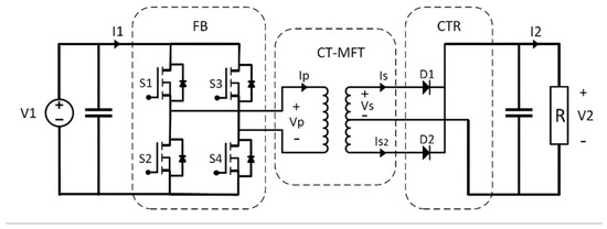
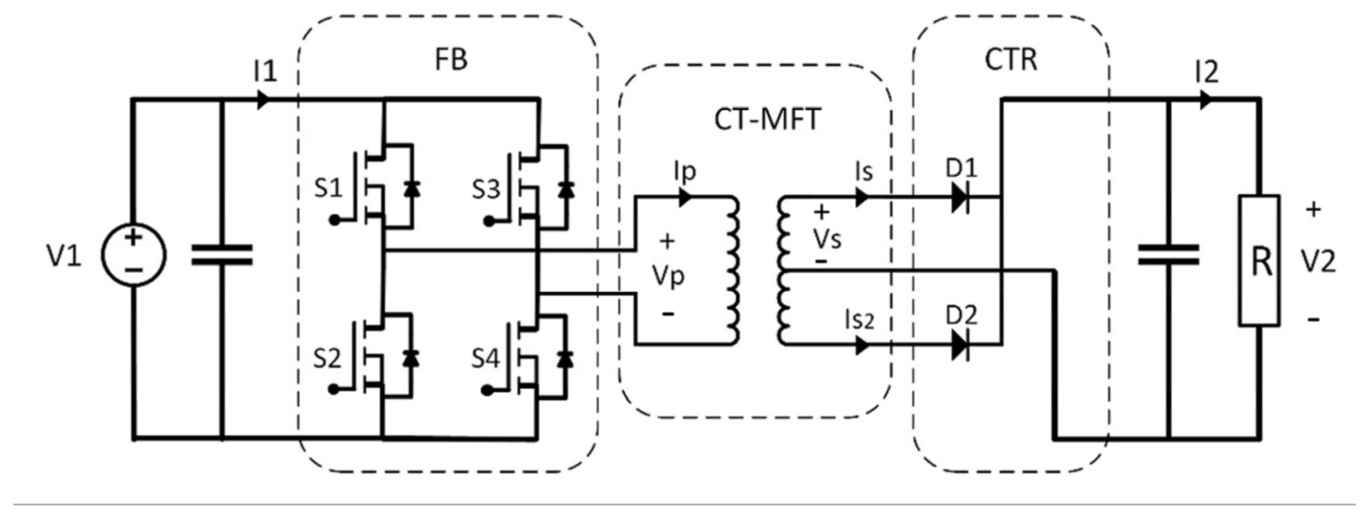
The PSFB topology has attracted increasing attention because of its simple structure and its ability to provide galvanic isolation, and was selected in this research due to the limitations in unidirectional applications [2,7,8,11]. The CT-PSFB consists of three stages: the active stage, the isolation stage, and the passive stage. The active stage consists of four active semiconductor devices (S1 to S4), connected in a FB structure. The isolation stage consists of the CT-MFT, and the detailed T model is presented in Section 3.3. Finally, the passive stage consists solely of two semiconductor diodes (D1 and D2) that form part of the center-tapped rectifier (CTR) structure. The structure of the CT-PSFB is shown in Figure 1.
Figure 1.
DC−DC CT-PSFB topology.
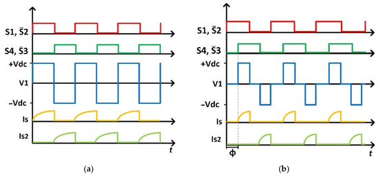
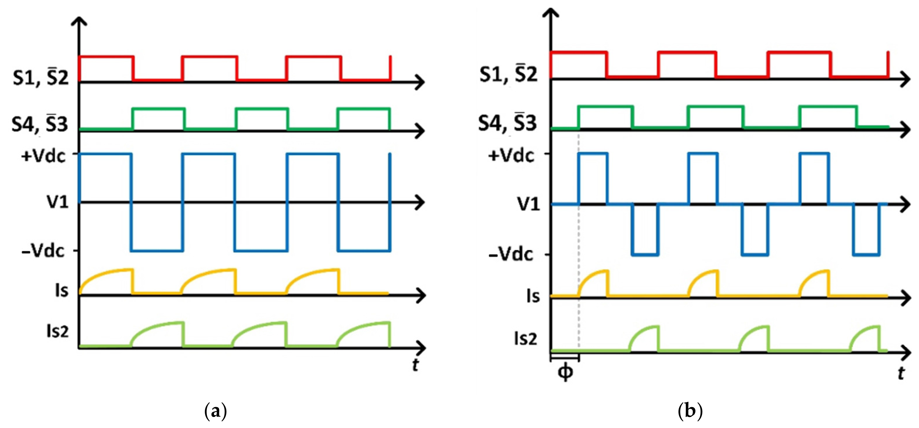
In the FB stage, the DC power supply is converted into medium-frequency AC power. In this range, SiC MOSFETs and a nanocrystalline core have demonstrated adequate performance. In Figure 1, Vp is the RMS voltage in the CT-MFT primary. The waveform of Vp depends directly on the phase angle (). The angle changes the signal and the THD value of the transformer power supply. The modulation implemented for the converter’s operation considers two main signals and two complementary signals. The main signals correspond to the modulations of S1 and S4, according to the diagram in Figure 1. The complementary signals are S2 and S3; each one includes a dead time to allow turn-off and turn-on in each leg of the FB. Each modulation runs at the nominal frequency with a 50% duty cycle. In this research, two angles serve as the references; they are at the limits of the modulation and cover the full 0° to 90° operating range. Under these conditions, the waveform in the CT-MFT power supply for the smallest angle is a two-level waveform, with a 50% duty cycle. At 90°, the waveform is a three-level waveform. Figure 2 shows the modulation, primary voltage, and secondary current waveforms for = 0° and 90°, respectively.
Figure 2.
CT-PSFB waveforms, (a) phase angle = 0°, and (b) phase angle = 90°.
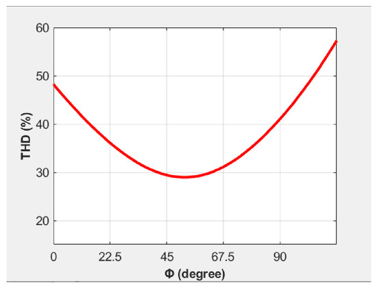
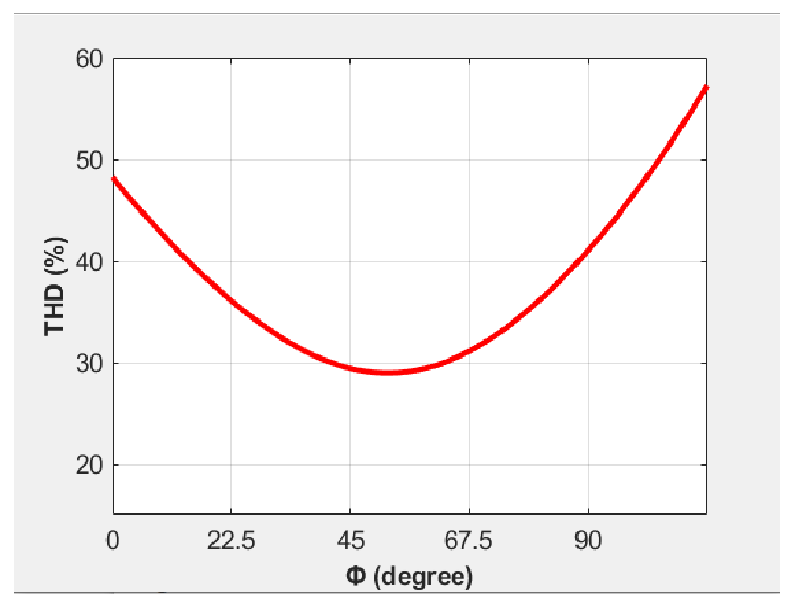
The THD behavior between 0° and 90° has a maximum of 48.34% at 0° and a minimum of 28.99% near 50°, as shown in Figure 3.
Figure 3.
Total Harmonic Distortion percentage related to .
3. CT-MFT Design Method for Non-Sinusoidal Voltage Feeding
A well-structured MFT design methodology allows specific operating conditions and characteristics to be addressed, for example, by considering a center tap and a non-sinusoidal power supply. The design method is key to overcoming specific technical constraints in converters. One of the main constraints is the difference in nominal operating voltages. Recent design methodologies focus on increasing efficiency and power density, as well as on lossless switching and modulation [12,13,23]. Design methodologies are continuously improving; however, there are specific configuration designs and operating conditions that have not been previously taken into consideration, such as feeding the MFT with a two- or three-level non-sinusoidal power supply while integrating a center tap in one of the secondary windings. Therefore, the first step in this work is to start with design methodologies for high-efficiency single-phase transformers.
The proposed design method takes [20] as a starting point. The adjustments in the methodology are carried out to achieve high performance and efficiency at different THD levels of the signal feeding the MFT. The incorporation of a center tap in the secondary winding changes the final size and power of the MFT. The changes in voltage level have a direct impact on the form factor (kf) and size of the prototype. Section 3.1 lists the steps involved in designing the transformer, detailing the considerations and updates needed when working under specific power supply conditions, such as two-level and multilevel power supplies with a range of different THD values. Section 3.2 addresses losses in the CT-MFT. Finally, Section 3.3 presents the T model of the CT-MFT in detail. By including improvements for specific conditions, the method ensures high-efficiency, reliable performance.
3.1. CT-MFT Design Methodology
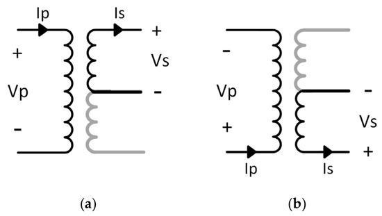
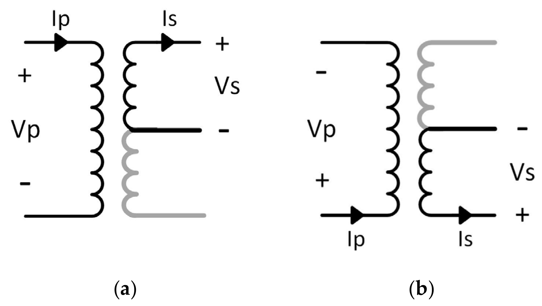
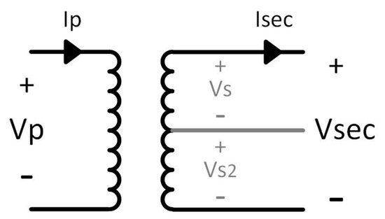
The CT-MFT can operate in two modes. This is advantageous and distinguishes it from other MFT configurations; the first mode, shown in Figure 4, uses the tap and one of the winding ends to transfer power.
Figure 4.
The first operating mode of the CT-MFT: (a) tap and upper winding, and (b) tap and lower winding.
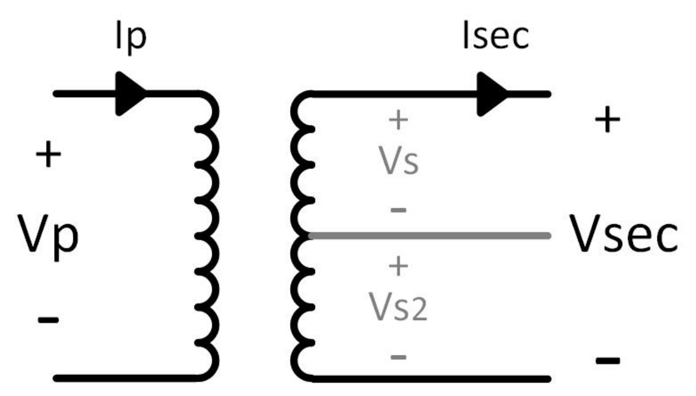
The second mode uses the full secondary winding to transfer power as a monophase transformer; the secondary voltage (Vsec) is present at the ends of the winding, as shown in Figure 5. The center tap takes part intermittently in the converter operation, as described in [20,21].
Figure 5.
The second option of CT-MFT operation.
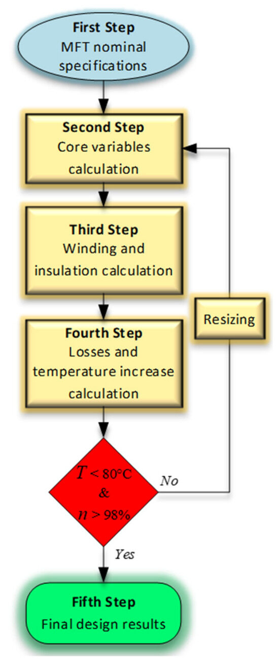
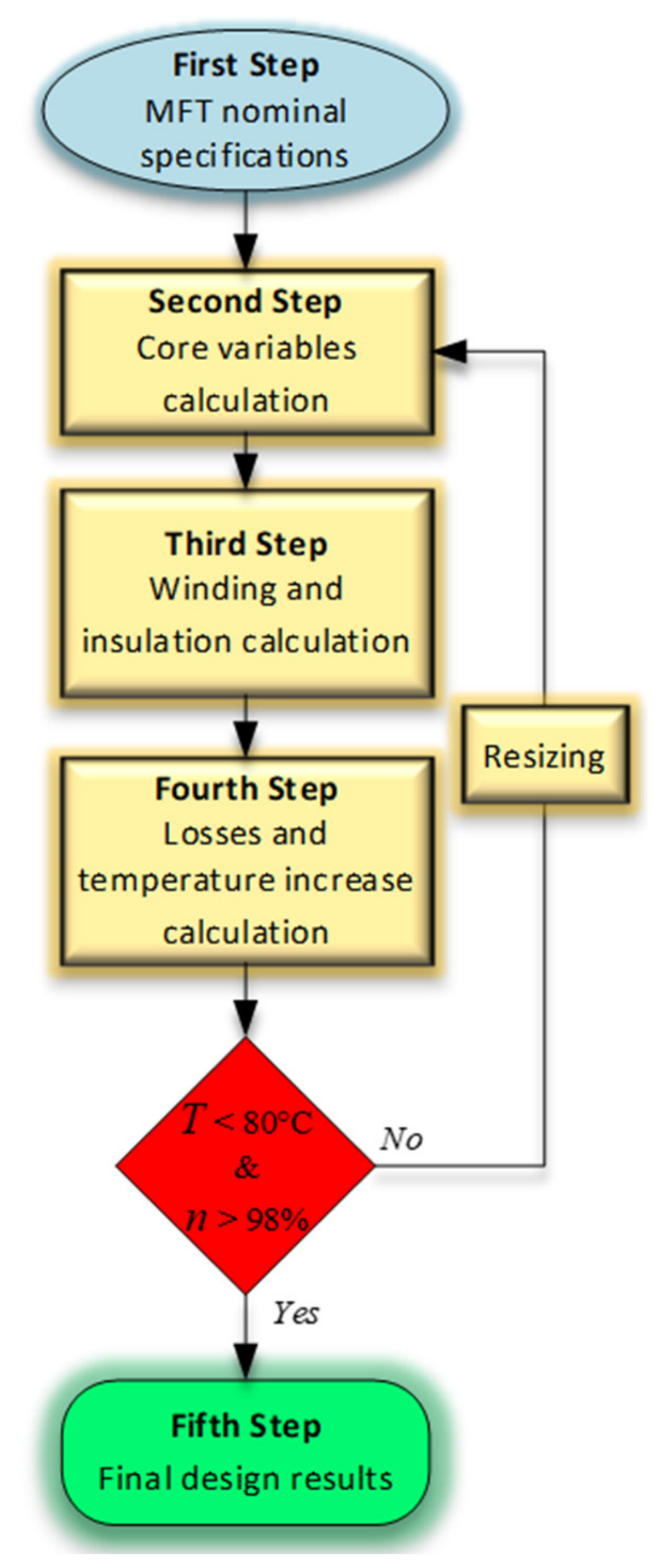
The new design methodology considers both operating modes but focuses mainly on the first mode because it is the most demanding operating condition for the CT-MFT. The steps of the proposed method are shown in Figure 6.
Figure 6.
Design steps of the CT-MFT.
First, the nominal MFT parameters are listed. Operating values are obtained directly from the application of interest. Such parameters are the primary and secondary voltages (Vp, Vs, and Vs2), output current (Is) (altogether considering the center tap), as well as the operating frequency (f), current density (J), turns ratio (a), waveform coefficient (kf), window utilization factor (ku), output power (Pout), input power (Pin), and converter output power (P2). For the CT-MFT to work properly with the CT-PSFB converter, three constraints are considered:
- (1)
- The waveform factor (kf);
- (2)
- The current density (J);
- (3)
- The effect of the tap on the secondary winding.
To address the first constraint, the waveform factors are kf = 4 for two-level signals, kf = 4.44 for sinusoidal signals, and for three-level signals kf is obtained with Equations (1) and (2), over the range 0° < < 180°.
is the angle of the positive voltage pulse in radians, and rad is the phase angle in radians. When the phase angle is in the range of 0° < < 180°, the value of kf increases, resulting in a decrease in the core size of the prototype. Therefore, for the first limitation, the design needs to be based on the device’s smallest operating phase angle. On the other hand, the most demanding case of kf occurs with a two-level signal ( = 0°), resulting in the largest core size in the prototype. By addressing this constraint, the CT-MFT operates without other limitations across the entire range of the CT-PSFB converter. Regarding the second constraint, it is common in MFT designs to use current densities (J) between 200 A/cm2 and 400 A/cm2 [18,19,20,24,25]. Regarding the skin and proximity effects, these are not relevant at medium frequencies for current densities up to 400 A/cm2 [19]. Therefore, this work uses a current density of 300 A/cm2, as it best balances winding resistance, thermal behavior, and core window area constraints. This increases the reliability and efficiency of the MFT prototype. The third constraint concerns the effect of non-sinusoidal waveforms with different THD levels on the CT-MFT. The design considers the tap in the secondary winding and the first operating mode. Additionally, values and operating conditions are considered to avoid performance degradation and are listed below:
- (1)
- The largest peak voltage;
- (2)
- Intermittent currents in the secondary winding, with respect to the tap;
- (3)
- Adjustment parameter in the output power (Pout).
The output power of the transformer in point three is Pout = P2 (U), where U is a factor applied due to the intermittent current in the secondary (U = 1.41), which corresponds to point 2 [24]. In this way, with the integration of the tap, the size of the prototype increases.
In the second step, two main characteristics are considered. Both are related to the core. These include its size, waveform, and center tap, which influence it, as well as its saturation limit. Some core materials are silicon steel, amorphous, nanocrystalline, and ferrite [17,20,26,27,28,29]. In the medium-frequency range (1 kHz to 20 kHz), silicon steel is an option, but due to its low flux density, an MFT cannot achieve high power densities [18]. The nanocrystalline core in an MFT excels in performance, efficiency, and power density due to its high permeability, low core losses, and high saturation flux density. This research uses nanocrystalline material and toroidal geometry due to their various advantages at 5 kHz [19,20].
The variables to be calculated are window area (Wa), effective core cross-section (Ac), area product (Ap), flux density (Bac), outside diameter (OD), core inside diameter (ID), and core length (HT). As a first step, the area product (Ap) is obtained to set the core size and thus determine the total power rating (Ptot) of the MFT, where Ptot = Pin + Pout, and Pin and Pout are described in the first step. The higher Pout, the higher the core size. In the second step, the value of flux density, Bac, is selected. For this work, this value is Bac = 0.75 × Bmax, where Bmax is the maximum flux density of the nanocrystalline material. Operating at 75% of Bmax provides a safety margin against transient overvoltages, preventing magnetic saturation while maximizing core utilization and power density. This value is selected to ensure reliable operation and prevent performance degradation [19,20].
In the third step, the primary and secondary winding turns (Np and Ns, respectively) and insulation are calculated. The MFT prototype in this work uses solid round copper wire. Besides determining Np and Ns, it is also necessary to obtain the cross-sectional area of the conductor for both windings (Awp for the primary and Aws for the secondary), the rated current at the input (Iin), the minimum distance between conductors (dcon), the insulation voltage required (Uins), and the dielectric strength of the insulation (Eins). The waveform and its peak value in each winding shape the calculation of all these variables. The sinusoidal signal is the most demanding for the MFT. The insulation for dry-type transformers is dins = (Uins/S × Eins), where dins is the minimum distance between conductors, and S is the safety margin. The maximum voltage in the secondary is twice the nominal voltage at the load; this is Vsec = Vs + Vs2. This is considered in the calculations.
In the fourth step, both the efficiency of the MFT prototype and the increase in core temperature are calculated. In this work, the goal is to achieve an efficiency (n) greater than 98% while keeping the temperature (T) below 80°C. To obtain these two values, the total losses in the transformer (Pt) are calculated, as described in [30], which in turn depend on four other parameters. These are the core losses (Pc), the copper losses (Pw), the magnetization inductance (Lm), and the total dispersion inductance (Ld) [19]. Copper losses are calculated as Pw = Pp + Ps, where Pp represents the primary winding losses, and Ps represents the secondary winding losses. Section 3.2 discusses these calculations in detail.
Regarding the increase in temperature in the core, Equations (3) and (4) are used [18,24].
where Tr is the increase in temperature in °C, Pt is the total loss in W, At is the transformer surface area in cm2, and Ks is a constant related to the core structure (Ks = 41.3 for laminated cores), Ac is the effective core cross-section, and Wa is the window area. If the efficiency and temperature increase targets are not met in the first iteration of step 4, then the area product and core size are adjusted by repeating steps 2 through 4 iteratively until the targets are reached. This iterative process is shown as the resizing block in Figure 6.
As a final step, the design results are collected, setting up the core variables (Wa, Ac, Ap), the winding variables (Np, Ns, Awp, Aws), and the required insulation properties. In these final design results, the core variables have values greater than the required core size. This is because the iterations converge on the commercial size of the next larger core. With the final design, the equivalent model of the CT-MFT is determined.
3.2. CT-MFT Losses
Losses in the CT-MFT are divided into winding losses and core losses. The former are calculated using Equations (5) and (6).
where Ip and Is are the CT-MFT primary and secondary currents, respectively, and Rp and Rs are the primary and secondary winding resistances, calculated using Equations (7) and (8), respectively.
MLT1 and MLT2 are the mean turn lengths of the primary and secondary windings, respectively. Np and Ns are the numbers of turns per winding, µΩ/cm1 and µΩ/cm2 are the resistances per centimeter of the primary and secondary winding conductors, respectively. The losses in the secondary winding are calculated for the nominal load and by considering the first operating mode. In this mode, half of the winding operates every 180°, but the power is continuously delivered to the nominal load.
Regarding the core losses, these depend on two factors: (a) operating frequency and (b) core material. Toroidal nanocrystalline cores have high permeability values and low specific core losses. The losses in nanocrystalline cores (Pc) are Pc = (P5k) × Wc, where P5k is the loss in the nanocrystalline material at the operating frequency in W/kg and Wc is the core weight in kg. Pc = 4.1 W at 5 kHz.
3.3. T Model of the CT-MFT
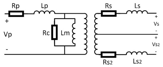
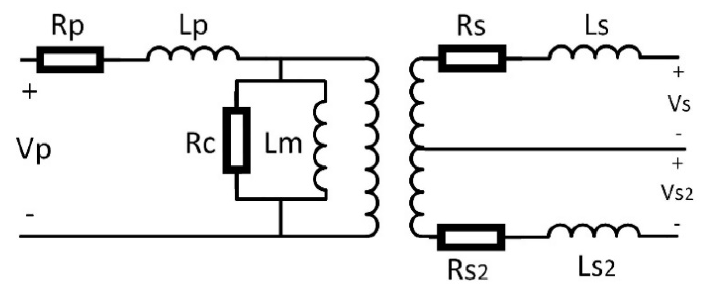
The T model of the transformer is selected because it represents the key parameters affecting the performance of the CT-MFT. The primary winding considers the resistance and inductance of the winding. The magnetization branch models the magnetization inductance and core losses. Each half of the center tap in the secondary winding has the same inductance and resistance. The model is simulated as described in Section 4.2. Table 1 lists the parameters for the design proposed in this paper. The implementation of the CT-MFT is described in Section 5. The detailed CT-MFT model is shown in Figure 7.
Table 1.
CT−MFT data for simulation.
Figure 7.
T model of the CT−MFT.
4. Performance Analysis of the CT-PSFB Topology
The performance analysis of the CT-PSFB structure requires a model capable of accurately describing each stage of the structure. The model must include semiconductor losses, as these affect the efficiency and reliability of the full converter.
Section 4.1 presents the loss models implemented for the semiconductor devices. Section 4.2 analyzes the efficiency of the CT-MFT under a sinusoidal power supply, which is a demanding condition for its evaluation. Finally, Section 4.3 examines the behavior of the CT-PSFB topology, focusing on the response of power, output voltage, and efficiency for the entire operating range evaluated.
4.1. Losses in the Semiconductors
SiC diodes and MOSFETs are both used as part of the electronic configuration of the CT-PSFB. The losses are obtained with (9) and (10) [30], respectively.
where Pdiode is the loss in the diode, Vf is the turn-on voltage, IF(rms) and IF(avg) are the RMS and average currents flowing through the diode, and RDon is the on-state resistance. MOSFETs have two loss mechanisms: switching losses and conduction losses. The switching losses are Pon and Poff. Conduction losses are determined by the on-state resistance (Ron) and IMrms, the RMS current through the device [30].
4.2. Performance of the CT-MFT
For the purposes of this work, the evaluation of the CT-MFT design considers the linear region of the B vs. H curve. This is valid because the flux density (Bac) is below the maximum flux density (Bmax). The CT-MFT data for simulation are presented in Table 1.
The first analysis corresponds to the CT-MFT with a resistive load and sinusoidal input, which represents the maximum instantaneous voltage. The measurement results and the efficiency obtained in the simulation are presented in Table 2.
Table 2.
CT-MFT efficiency with sinusoidal input.
4.3. Performance of the DC-DC CT-PSFB Converter
To estimate the efficiency of the converter, the phase angle varies from 0° to 90°. The input voltage and load remain fixed at nominal values to isolate the topology’s behavior under phase shift variations, an approach that is highly useful in constant load applications for regulating power transfer. The parameters of the MOSFETs are estimated using Equations (9) and (10) for the diodes. The T model data of the CT-MFT are detailed in Table 1.
Table 3 presents the efficiency and measurements of the CT-PSFB operating at 25° and 90° phase angles. The differences in efficiency are due to variations in the turn-on time of the semiconductor devices and changes in the power values supplied.
Table 3.
Efficiency of the CT-PSFB operating with different phase angles.
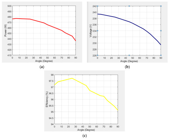
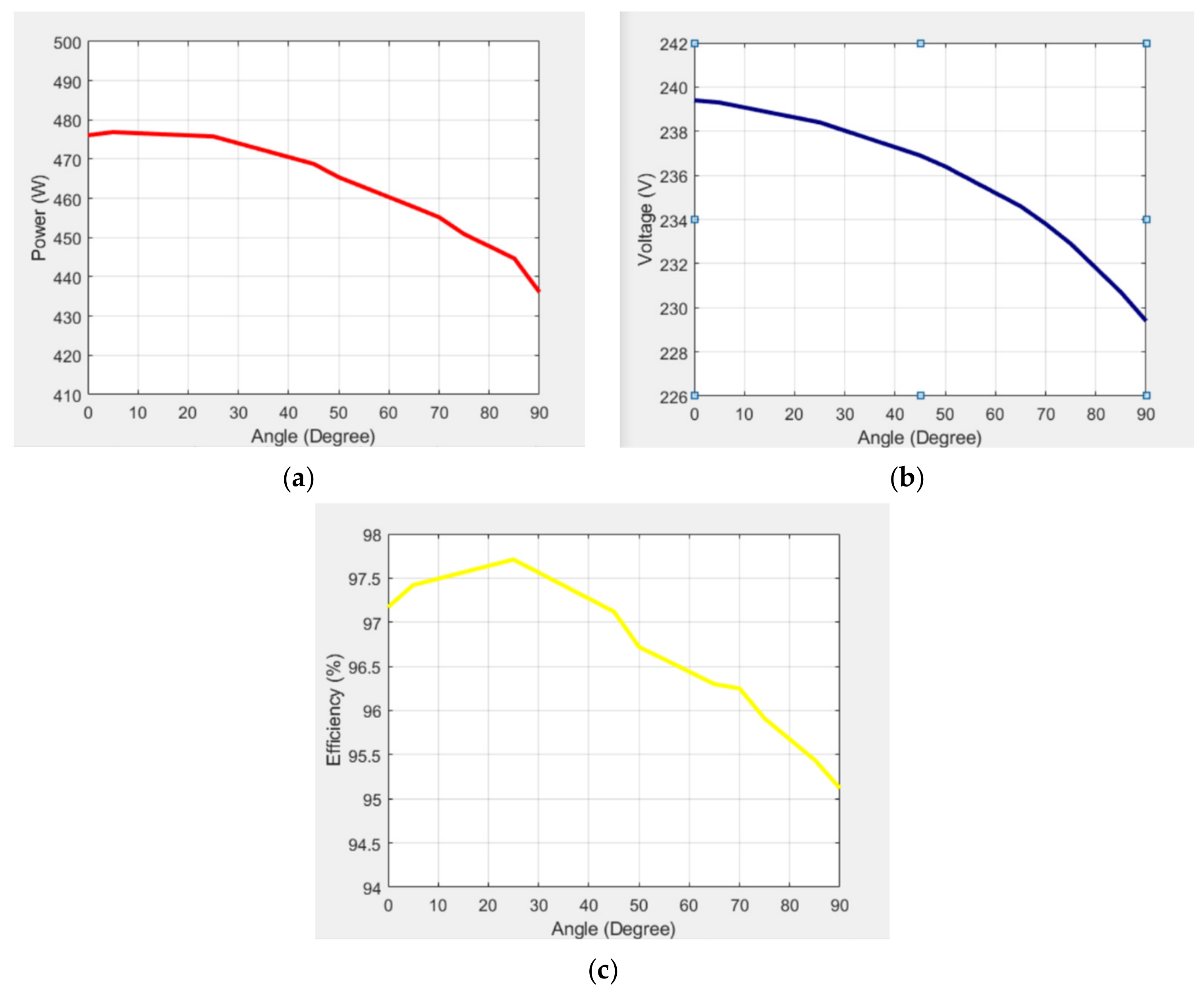
Figure 8 illustrates the relationships between power, output voltage, and efficiency with respect to the phase angle in the converter. The output voltage is affected by the phase angle, which allows the voltage to be regulated under a fixed load. This characteristic is especially important in batteries, where the terminal voltage is related to the state of charge (SOC) [1,4,10]. The system operates with an efficiency greater than 95% in the range of 0° to 90°, despite the waveform and THD variations in the transformer power supply.
Figure 8.
CT-PSFB simulation at different phase angle: (a) Power in the load, (b) Voltage in the load (V2) and, (c) Efficiency.
5. Experimental Validation
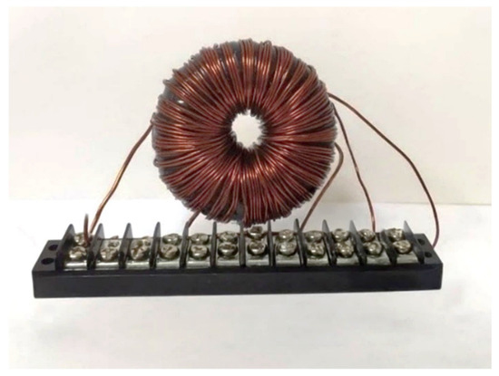
To experimentally validate the CT-MFT, a laboratory prototype is implemented. The data are presented in Table 4. The secondary winding is built symmetrically, aligning one turn of the upper winding (Ns_u) next to one of the lower windings (Ns_L), to ensure an equivalent model and identical induced voltage at both ends. Figure 9 shows the final prototype.
Table 4.
CT-MFT data.
Figure 9.
CT-MFT prototype, P2 = 500 W and 5 kHz.
5.1. Efficiency of CT-MFT Prototype
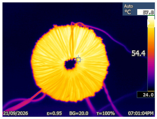
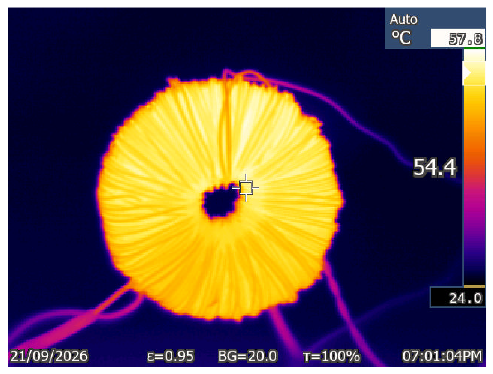
The CT-MFT prototype reaches an efficiency of 99.65% under sinusoidal conditions. The resulting waveforms are presented in Figure 10. (Tektronix TBS1104 oscilloscope; Beaverton, OR, USA, Fluke 80i 1000s current probe; Everett, WA, USA, and Agilent 6834B power supply; Santa Clara, CA, USA). Furthermore, to evaluate the CT-MFT temperature rise, Figure 11 provides a steady-state thermographic profile captured at a controlled ambient temperature of 25 °C (Fluke Ti32).
Figure 10.
CT-MFT prototype voltages (CH1-yellow is Vp and CH2-magenta is Vs) and currents (CH3-violet is Ip and CH4-green is Is). Efficiency = 99.65%.
Figure 11.
Steady-state thermography of the CT-MFT. The central marker shows a representative region temperature of 54.4 °C (peak scale at 57.8 °C).
5.2. Efficiency of DC-DC CT-PSFB Prototype
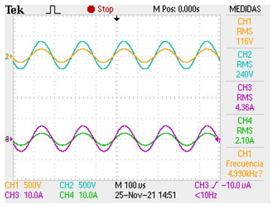
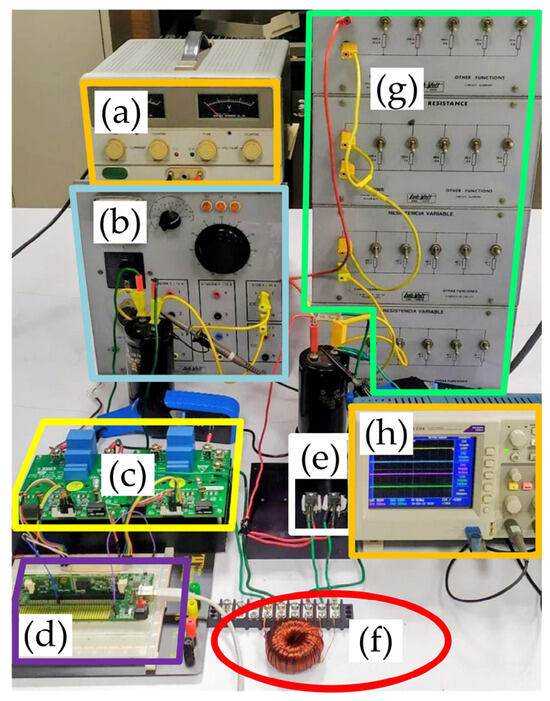
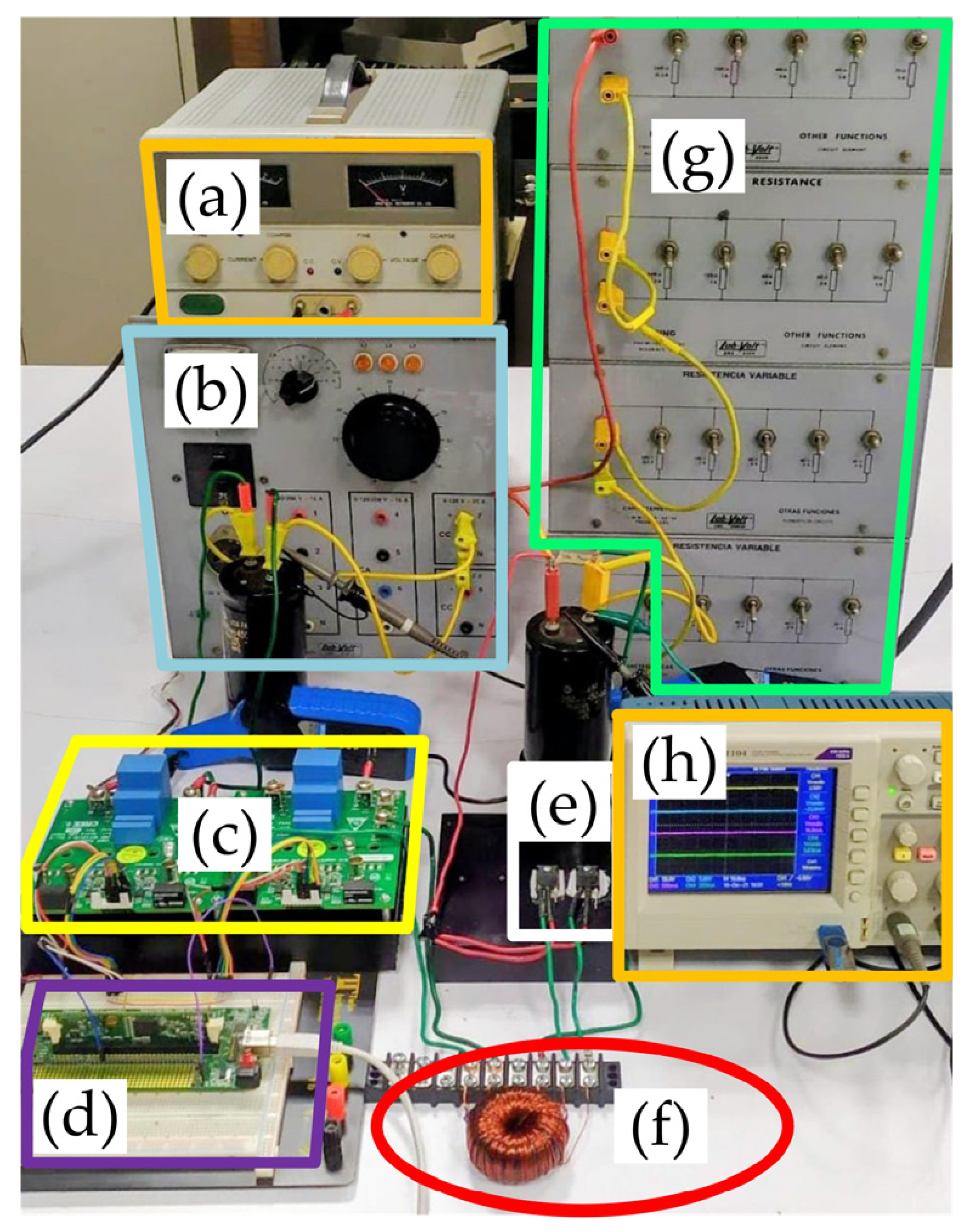
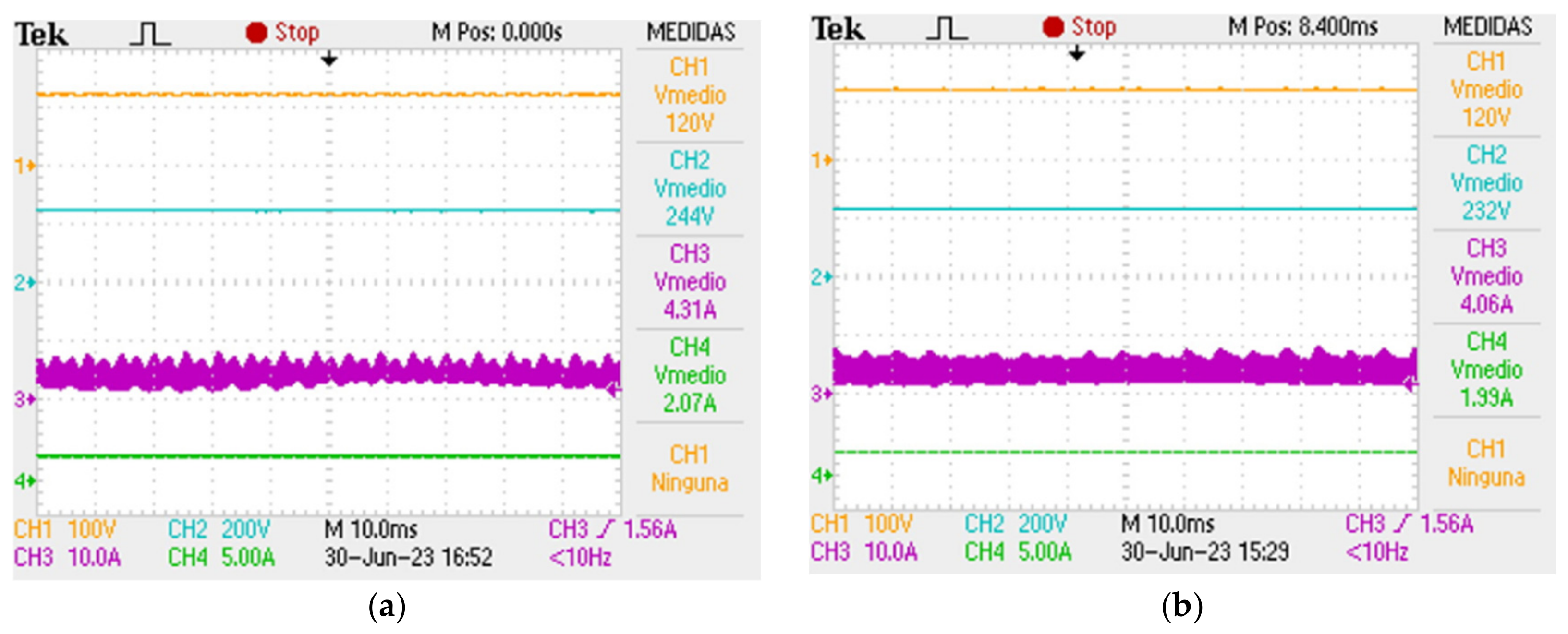
Figure 12 shows the CT-PSFB converter including the CT-MFT prototype. Figure 13 shows the input–output waveforms of this configuration.
Figure 12.
CT-PSFB topology, (a) 12 V DC source, (b) DC source 0–120 V, (c) FB (C2M0080120D), (d) DSP (S28335), (e) diodes (C4D20120D), (f) CT-MFT, (g) load, and (h) oscilloscope.
Figure 13.
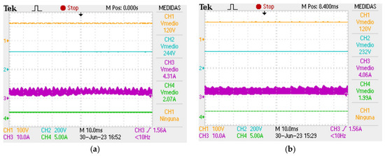
CT-PSFB converter waveforms at the source (V1 is CH1-yellow, I1 is CH3-purple) and load (V2 is CH2-cyan, I2 is CH4-green), (a) 25° with 97.66% efficiency, and (b) 90° with 94.76% efficiency.
The highest efficiency is 97.66% at a phase angle of 25° and a 244 V load voltage. On the other hand, for the 90° angle, the efficiency is 94.76% at a 232 V load voltage. The latter is the lowest efficiency obtained. The resulting waveforms are presented in Figure 12.
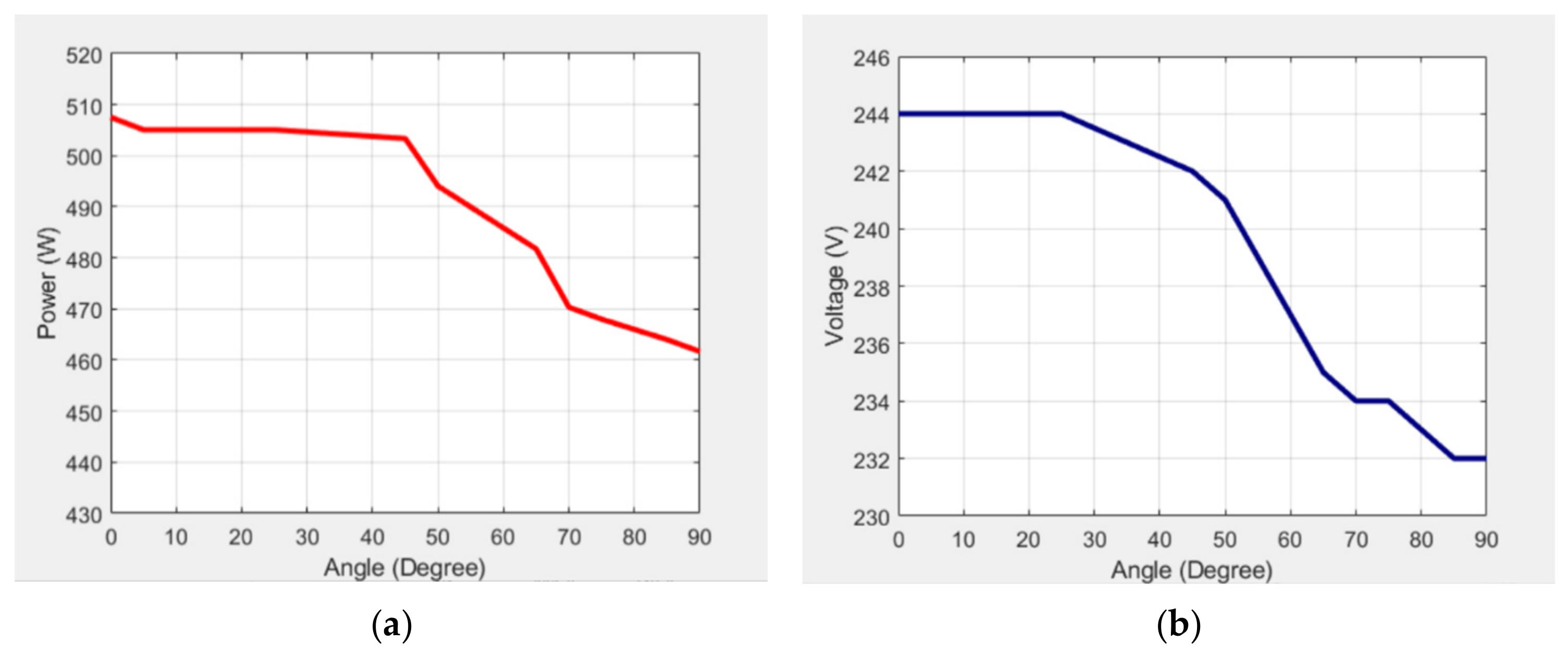
Furthermore, when comparing the simulation results with the experimental efficiency values presented above, a maximum deviation of only 0.34% is found. This minimal discrepancy is directly attributed to the inherent measurement tolerances of the equipment used, specifically the oscilloscope probes (voltage ±1.75% errors and ±1.5% 5mA errors in Hantek CC-65 current clamps). Subsequently, Figure 14 shows the behavior of the output power and the load voltage vs. the phase angle. As can be observed, the power varies from 502 W to 460 W. In this 42 W variation range, the converter efficiency does not fall below 94.76%. Regarding the 12 V variation in the load voltage, this margin is meaningful because various applications require precise control of the voltage. If there is a variation in the supply voltage, it is possible to compensate for it through converter modulation. Likewise, the load voltage can be fixed through modulation, ensuring a controllable power supply.
Figure 14.
CT-PSFB prototype at different phase angles: (a) Power (Pout), and (b) Voltage in the load (V2).
The experimental results confirm the effectiveness of the proposed design, validating its performance both through efficiency tests with a sinusoidal power supply and within the CT-PSFB topology under non-sinusoidal waveforms. The converter maintains an efficiency greater than 94.76% across the entire operating range and reaches a maximum value of 97.66%, showing the viability of the model for applications in high-efficiency isolated DC-DC converters that incorporate a center tap in a winding.
6. Discussion
The proposed design method for the CT-MFT ensures adequate device performance from the conceptual stage by considering non-sinusoidal input conditions and center-tapped configurations. Furthermore, the choice of nanocrystalline material for the core [20,21] and SiC for the semiconductors [23,30] ensures reliability and high efficiency in the CT-PSFB. Galvanically isolated DC-DC converters are essential, and the tailor-made transformer is a critical component for proper connection. This device ensures efficient and safe interconnection in solar generation, electromobility, and energy storage applications [1,2,3,4,5,6,7,8,9]. To validate this approach, Table 5 presents a comparison of various DC-DC converters based on isolated topologies.
Table 5.
Comparison of DC-DC converters.
Table 5 reveals that references focused on the custom design of transformers tend to omit the experimental efficiency of the converter [1,11,12,13,14,15,16,17,18,25]. This omission, coupled with the absence of information on the core material, limits the reproducibility of the prototypes, as it does not provide a clear reference for the performance of the prototype and its design. Similarly, the lack of a detailed model overlooks various effects present in high-efficiency transformers and DC-DC topologies. Generally, only leakage inductance is considered, while the rest of the transformer effects are ignored.
Regarding the number of elements, this research stands out for using a minimal number of semiconductors, eliminating two devices in the rectification stage. Although Refs. [12,20] achieve the same reduction in the number of devices, they have operational limitations. Ref. [12] focuses its contribution on the control strategy, omitting power, converter efficiency, and the detailed design of the CT-MFT. On the other hand, Ref. [20] reports competitive efficiency; however, the CT-MFT’s power supply is restricted to two levels and nominal power. The proposed method allows for variations in the phase angle while maintaining high performance; furthermore, the validated prototype achieves an efficiency of 97.66% at full load. Thus, isolated topologies requiring a CT-MFT can directly incorporate the proposed method, ensuring high efficiency and reliability.
7. Conclusions
This paper presents a customized design method for center-tapped medium-frequency transformers driven by non-sinusoidal input waveforms with varying signal levels and THD. Its application is focused on high-efficiency isolated converters that require versatility across a range of operating conditions, rather than just a single operating point. To this end, a high-efficiency CT-MFT was designed and validated in the CT-PSFB topology. The operating range corresponds to two-level and multilevel signals with different THD values.
The detailed model of the topology was simulated, and the experimental validation confirms that the use of silicon carbide (SiC) semiconductors and a nanocrystalline core ensures proper operation. The experimental results confirm the CT-MFT’s excellent performance, operating at an efficiency of 99.65% under the most demanding signals and at rated power. Likewise, validation of the CT-PSFB converter confirmed superior performance, showing a peak efficiency of 97.66% at 25° of operation and efficiency exceeding 94.7% across the entire study range (0° to 90° of phase). Similarly, the tests confirmed variations of 22.5% in the THD of the feed signal. On the other hand, the main disadvantage of this proposal is the reduction in power density. This occurs due to an increase in the final size and winding volume of the CT-MFT prototype, a direct consequence of the transformer’s utilization factor and the requirement for a doubled secondary winding to include the center tap. However, the topology offers significant advantages. Foremost, conduction losses are substantially reduced because two passive semiconductors are eliminated; during rectification, only one forward-biased diode voltage drop occurs per half-cycle, increasing the converter’s overall efficiency. The design method stipulates that the CT-MFT design should be based on the smallest phase angle to which it will be subjected and the need for a center tap; both parameters affect the final size of the prototype.
These results demonstrate the effectiveness of the topology and confirm that the proposed method ensures proper operation of the CT-MFT in converters that alter its input waveform, without compromising performance.
Author Contributions
Conceptualization, J.O.-M. and G.A.A.-R.; methodology, J.O.-M. and G.A.A.-R.; software, J.O.-M. and G.A.A.-R.; validation, J.O.-M., G.A.A.-R. and V.V.-R.; formal analysis, J.O.-M. and G.A.H.-P.; investigation, J.O.-M. and G.A.A.-R.; resources, E.L.M.-G.; data curation, J.O.-M. and V.V.-R.; writing—original draft preparation, J.O.-M.; writing—review and editing, G.A.H.-P., E.L.M.-G. and V.V.-R.; visualization, G.A.A.-R. and J.O.-M.; supervision, E.L.M.-G. and V.V.-R.; project administration, E.L.M.-G.; funding acquisition, E.L.M.-G. All authors have read and agreed to the published version of the manuscript.
Funding
This research received no external funding.
Data Availability Statement
The original contributions presented in this study are included in the article.
Acknowledgments
The authors thank the UCEMICH (Universidad de la Cienega del estado de Michoa-cán de Ocampo) and PGIIE (Programa de Graduados e Investigación en Ingeniería Eléc-trica, TNM/ITM) for supporting our research and projects, which led to the writing of the present paper.
Conflicts of Interest
The authors declare no conflicts of interest.
Abbreviations
The following abbreviations are used in this manuscript:
| MFT | Medium-frequency transformer |
| THD | Total harmonic distortion |
| CT-MFT | Central-tapped medium-frequency transformer |
| CT-PSFB | Central-tapped phase-shift full-bridge |
| ZCS | Zero current switching |
| WPT | Wireless power transfer |
| IPT | Inductive power transfer |
| SAB | Single active bridge |
| PSFB | Phase-shift full-bridge |
| DAB | Dual active bridge |
| TAB | Triple active bridge |
| G2V | Grid-to-vehicle |
| ZVS | Zero-voltage switching |
| SOC | State of charge |
| Φ | Phase angle |
| Vp | RMS voltage in the CT-MFT primary |
| kf | Waveform coefficient |
| Vsec | Secondary voltage |
| Vs | Secondary voltage in upper wind |
| Vs2 | Secondary voltage in lower wind |
| Is | Output current |
| f | Operating frequency |
| J | Current density |
| a | Turns ratio |
| ku | Window utilization factor |
| Pout | Output power |
| Pin | Input power |
| P2 | Converter output power |
| Θon | Angle of the positive voltage pulse in radians |
| Φrad | Phase angle in radians |
| U | Factor applied due to the intermittent current in the secondary |
| Wa | Window area |
| Ac | Effective core cross-section |
| Ap | Area product |
| Bac | Flux density |
| OD | Outside diameter |
| ID | Core inside diameter |
| HT | Core length |
| Ptot | Total power rating |
| Bmax | Maximum flux density of the nanocrystalline material |
| Np | Primary winding turns |
| Ns | Secondary winding turns |
| Awp | Primary conductor area |
| Aws | Secondary conductor area |
| Iin | Rated current at the input |
| dcon | Minimum distance between conductors |
| Uins | Insulation voltage required |
| Eins | Dielectric strength of the insulation |
| S | Safety margin |
| n | Efficiency |
| T | Temperature |
| Pt | Total losses in the transformer |
| Pc | Core losses |
| Pw | Copper losses |
| Lm | Magnetization inductance |
| Ld | Total dispersion inductance |
| Tr | Increase in temperature in °C |
| At | Transformer surface area in cm2 |
| Ks | A constant related to the core structure |
| Ip | CT-MFT primary current |
| Is | CT-MFT secondary current |
| Rp | Primary winding resistance |
| Rs | Secondary winding resistance upper |
| Rs2 | Secondary winding resistance lower |
| Lp | Primary dispersion inductance |
| Ls | Secondary dispersion inductance upper |
| Ls2 | Secondary dispersion inductance lower |
| Rc | Magnetization resistance |
| Lm | Magnetizing inductances |
| MLT1 | Mean turn length of the primary winding |
| MLT2 | Mean turn length of the secondary winding |
| Pc | Losses in nanocrystalline cores |
| P5k | Losses in the nanocrystalline material at the operating frequency in W/kg |
| Wc | Core weight in kg |
| Pdiode | Losses in the diode |
| Vf | Turn-on voltage of the diode |
| IF(rms) | RMS current flowing through the diode |
| IF(avg) | Average current flowing through the diode |
| RDon | On-state resistance in the diode |
| Pon | On-state switching losses in MOSFETs |
| Poff | Off-state switching losses in MOSFETs |
| Ron | On-state resistance in MOSFETs |
| IMrms | RMS current through MOSFETs |
| Ns_u | Turn of the upper winding |
| Ns_L | Turn of the lower winding |
| µr | Relative permeability |
| P | Converter output power |
References
- Gabriel, M.T.; Mansour, D.-E.A.; Shoyama, M.; Abdelkader, S.M. Design and performance evaluation of a battery-integrated PV system utilizing triple-active bridge based solid-state transformer topology. J. Energy Storage 2025, 114, 115646. [Google Scholar] [CrossRef] [Scilit]
- Mojlish, S.A.K.; Sutanto, D.; Muttaqi, K.M. Impacts of ultra-fast charging of electric vehicles on power grids: State-of-the-art technologies, case studies, and a proposed improvement using a solid-state transformer. J. Energy Storage 2025, 107, 114913. [Google Scholar] [CrossRef] [Scilit]
- Zhaksylyk, A.; Rasool, H.; Abramushkina, E.; Chakraborty, S.; Geury, T.; El Baghdadi, M.; Hegazy, O. Review of Active Front-End Rectifiers in EV DC Charging Applications. Batteries 2023, 9, 150. [Google Scholar] [CrossRef] [Scilit]
- Abraham, D.S.; Verma, R.; Kanagaraj, L.; Giri Thulasi Raman, S.R.; Rajamanickam, N.; Chokkalingam, B.; Marimuthu Sekar, K.; Mihet-Popa, L. Electric Vehicles Charging Stations’ Architectures, Criteria, Power Converters, and Control Strategies in Microgrids. Electronics 2021, 10, 1895. [Google Scholar] [CrossRef] [Scilit]
- Darwish, A. A modular step-up DC/DC converter for electric vehicles. Energies 2024, 17, 6305. [Google Scholar] [CrossRef] [Scilit]
- Ali, A.; Mousa, H.H.H.; Shaaban, M.F.; Azzouz, M.A.; Awad, A.S.A. A Comprehensive Review on Charging Topologies and Power Electronic Converter Solutions for Electric Vehicles. J. Mod. Power Syst. Clean Energy 2024, 12, 675–694. [Google Scholar] [CrossRef] [Scilit]
- Shahed, M.T.; Rashid, A.B.M.H. Battery charging technologies and standards for electric vehicles: A state-of-the-art review, challenges, and future research prospects. Energy Rep. 2024, 11, 5978–5998. [Google Scholar] [CrossRef] [Scilit]
- Jeong, S.-G.; Kwon, J.-M.; Kwon, B.-H. High-efficiency bridgeless single-power-conversion battery charger for light electric vehicles. IEEE Trans. Ind. Electron. 2019, 66, 215–222. [Google Scholar] [CrossRef] [Scilit]
- Bunyamin, W.M.H.W.; Baharom, R.; Munim, W.N.W.A.; Zolkiffly, M.Z.; Ahmad, A.S. Advancements in electrical systems for E-bike battery charging: A technical examination of conventional and wireless power transfer technologies. Int. J. Power Electron. Drive Syst. 2024, 15, 1617–1632. [Google Scholar] [CrossRef] [Scilit]
- Yildiriz, E.; Bayraktar, M. Design and Implementation of a Wireless Charging System Connected to the AC Grid for an E-Bike. Energies 2022, 15, 4262. [Google Scholar] [CrossRef] [Scilit]
- Sayed, K.; Ali, Z.M.; Aldhaifallah, M. Phase-Shift PWM-Controlled DC–DC Converter with Secondary-Side Current Doubler Rectifier for On-Board Charger Application. Energies 2020, 13, 2298. [Google Scholar] [CrossRef] [Scilit]
- Lee, Y.J.; Bak, Y.; Lee, K.-B. Control Method for Phase-Shift Full-Bridge Center-Tapped Converters Using a Hybrid Fuzzy Sliding Mode Controller. Electronics 2019, 8, 705. [Google Scholar] [CrossRef] [Scilit]
- Ataullah, H.; Iqbal, T.; Khalil, I.U.; Ali, U.; Blazek, V.; Prokop, L.; Ullah, N. Analysis of the Dual Active Bridge-Based DC-DC Converter Topologies, High-Frequency Transformer, and Control Techniques. Energies 2022, 15, 8944. [Google Scholar] [CrossRef] [Scilit]
- Cai, X.; Liu, Y.; Zhu, Y.; Zhou, Y.; Luo, C.; Liu, Q. ISOS-SAB DC/DC Converter for Large-Capacity Offshore Wind Turbine. Energies 2024, 17, 5071. [Google Scholar] [CrossRef] [Scilit]
- Predescu, D.-M.; Roșu, Ș.-G. Solid state transformers: A review—Part I: Stages of conversion and topologies. Technologies 2025, 13, 74. [Google Scholar] [CrossRef] [Scilit]
- Predescu, D.-M.; Roșu, Ș.-G. Solid-state transformers: A review—Part II: Modularity and applications. Technologies 2025, 13, 50. [Google Scholar] [CrossRef] [Scilit]
- Gao, S.; Chen, W.; Zhao, H.; Liu, C. Full-Bridge Intermediate-Frequency Converter with Low Voltage and Current Stress on Auxiliary Switching Devices. Energies 2026, 19, 852. [Google Scholar] [CrossRef] [Scilit]
- Huang, P.; Mao, C.; Wang, D.; Wang, L.; Duan, Y.; Qiu, J.; Xu, G.; Cai, H. Optimal Design and Implementation of High-Voltage High-Power Silicon Steel Core Medium-Frequency Transformer. IEEE Trans. Ind. Electron. 2017, 64, 4391–4401. [Google Scholar] [CrossRef] [Scilit]
- Sandoval-Valencia, T.; Ruiz-Robles, D.; Ortíz-Marín, J.; Franco, J.A.; Hernandez-Escobedo, Q.; Moreno-Goytia, E. Isolated High-Gain DC-DC Converter with Nanocrystalline-Core Transformer: Achieving 1:16 Voltage Boost for Renewable Energy Applications. Technologies 2024, 12, 246. [Google Scholar] [CrossRef] [Scilit]
- Ortíz-Marín, J.; Ruiz-Robles, D.; Moreno-Goytia, E.L.; Venegas-Rebollar, V. Design and implementation of a Central-Tapped Medium Frequency Transformer with nanocrystalline core for high-efficiency DC-DC SAB converters. Electr. Power Syst. Res. 2024, 227, 109900. [Google Scholar] [CrossRef] [Scilit]
- Lim, C.-Y.; Jeong, Y.; Moon, G.-W. Phase-Shifted Full-Bridge DC–DC Converter With High Efficiency and High-Power Density Using Center-Tapped Clamp Circuit for Battery Charging in Electric Vehicles. IEEE Trans. Power Electron. 2019, 34, 10945–10959. [Google Scholar] [CrossRef] [Scilit]
- Qin, G.; Ma, H.; Lei, J.; Hao, C. Advanced Control Strategies for Enhancing the Performance of Phase-Shifted Full-Bridge Series Resonant DC–DC Converters in Photovoltaic Micro-Inverters. Energies 2025, 18, 387. [Google Scholar] [CrossRef] [Scilit]
- Ortíz-Marín, J.; Gallo-Reyes, D.; Ruiz-Robles, D.; Venegas-Rebollar, V. Analyzing Power Losses and Performance of an Isolated DC-DC Converter for Renewable Energies Systems. Electronics 2023, 12, 1110. [Google Scholar] [CrossRef] [Scilit]
- McLyman, C.W.T. Transformer and Inductor Design Handbook, 4th ed.; CRC Press: Boca Raton, FL, USA, 2011; ISBN 978-1-4398-3688-0. [Google Scholar]
- Bahmani, M.A.; Thiringer, T.; Kharezy, M. Design Methodology and Optimization of a Medium-Frequency Transformer for High-Power DC–DC Applications. IEEE Trans. Ind. Appl. 2016, 52, 4225–4233. [Google Scholar] [CrossRef] [Scilit]
- Khatua, M.; Kumar, A.; Pervaiz, S.; Chakraborty, S.; Afridi, K.K. A Single-Stage Isolated AC–DC Converter Based on the Impedance Control Network Architecture. IEEE Trans. Power Electron. 2021, 36, 10366–10382. [Google Scholar] [CrossRef] [Scilit]
- Jafari, M.; Malekjamshidi, Z.; Lei, G.; Wang, T.; Platt, G.; Zhu, J. Design and Implementation of an Amorphous High-Frequency Transformer Coupling Multiple Converters in a Smart Microgrid. IEEE Trans. Ind. Electron. 2017, 64, 1028–1037. [Google Scholar] [CrossRef] [Scilit]
- Guo, Z.; Cao, B.; Chen, C.; Huang, A.Q. A Review of High-Power Medium Frequency Transformers in Medium Voltage Power Electronics: State of the Art, Challenges, and Solutions. IEEE Trans. Power Electron. 2026, 41, 9422–9436. [Google Scholar] [CrossRef] [Scilit]
- Ruiz, D.; Ortíz, J.; Moreno, E.; Fuerte, C.; Venegas, V.; Vargas, A.; Vergara, H. Ferrites and Nanocrystalline Alloys Applied to DC–DC Converters for Renewable Energies. Appl. Sci. 2022, 12, 709. [Google Scholar] [CrossRef] [Scilit]
- Gallo-Reyes, D.; Alvarez-Marin, I.; Ortiz-Marin, J.; Ruiz-Robles, D.; Venegas-Rebollar, V.; Moreno-Goytia, E.L. Accurate analytical calculation of losses and efficiency in full-bridge DC-DC converter. In Proceedings of the 2022 IEEE International Autumn Meeting on Power, Electronics and Computing (ROPEC), Ixtapa, Mexico, 9–11 November 2022; pp. 1–6. [Google Scholar] [CrossRef] [Scilit]

Disclaimer/Publisher’s Note: The statements, opinions and data contained in all publications are solely those of the individual author(s) and contributor(s) and not of MDPI and/or the editor(s). MDPI and/or the editor(s) disclaim responsibility for any injury to people or property resulting from any ideas, methods, instructions or products referred to in the content. |
© 2026 by the authors. Licensee MDPI, Basel, Switzerland. This article is an open access article distributed under the terms and conditions of the Creative Commons Attribution (CC BY) license.