


Abstract
Lead halide-based perovskite solar cells have gained significant attention from academia and the photovoltaic industry due to their exceptional optical and electrical characteristics. The primary problem with Pb-based perovskite pertains to its toxicity and solubility in water within the external environment. These concerns regarding hazards to the environment are constraining the application of lead-based perovskite in both consumer and industrial contexts. To offer a viable alternative to lead-based hazardous perovskite solar cells, we examined an inverted (p-i-n) perovskite structure with three distinct absorber layers based on cesium bismuth halides (Cs3Bi2I9, Cs3Bi2Cl9, Cs3Bi2Br9) and conducted a comparative analysis utilizing SCAPS-1D software (version 3.3.08). The comparison analysis of our design against starting parameters indicated that the optimal power conversion efficiency (PCE) of 10.01% was recorded for Cs3Bi2I9, 7.56% for Cs3Bi2Br9, and 4.34% for Cs3Bi2Cl9. Following careful optimization of the thickness of charge-transport layers (CTLs), doping concentrations of CTLs, and all three absorber layers, the overall efficiencies of the three inverted structures were enhanced from 10.01% to 14.08% for Cs3Bi2I9, from 4.34% to 5.28% for Cs3Bi2Cl9, and from 7.56% to 11.05% for Cs3Bi2Br9, respectively. The other performance enhancement, open-circuit voltage, increased from 1.08 V to 1.37 V for Cs3Bi2I9, from 1.26 V to 1.47 V for Cs3Bi2Cl9, and from 1.20 V to 1.47 V for Cs3Bi2Br9. This comparative analysis of proposed perovskite devices demonstrates that Cs3Bi2X-based perovskite devices possess significant potential to replace conventional hazardous solar cells in the renewable and clean energy sectors.
1. Introduction
The energy requirements are escalating swiftly due to industrialization and commercialization in both developed and underdeveloped countries [1,2]. Conventional methods of power generation utilizing coal, gas, and gasoline are inadequate to address the energy issue intensified by population growth, and these resources are finite and will deplete over time [3]. Conventional energy sources are limited and negatively affect human health by increasing carbon emissions, which contribute to global warming and worsen diseases such as asthma and cardiovascular conditions [4]. It is imperative to identify alternate methods, such as renewable energy sources (solar, wind, biogas, etc.), for power generation to address the energy problem. Among all renewable energy sources, solar cells are a prominent contender for ecologically sustainable and cost-effective power generation [5,6]. The need for solar cells has expanded over time; nonetheless, a primary worry is the elevated cost of manufacturing solar cells for large-scale integration. Perovskite solar cells are considered a leading prospect in the solar cell market due to their expected lowered manufacturing costs in the near future [6,7].
The chemical composition of the perovskite material is ABX3, where X represents halogen atoms (anions, e.g., chlorine (Cl), bromine (Br), and iodine (I)), B represents divalent cations (lead (Pb2+), tin (Sn2+), bismuth (Bi2+), etc.), and A represents monovalent cations such as methylammonium cation (CH3NH3+ or MA+), formamidinium cation (HC(NH2)2+ or FA+), and caesium (Cs+). In the crystalline structure of perovskite, the A ion is mostly surrounded by eight three-dimensional configurations formed by corner-sharing octahedral BX6 units [8,9]. The chemical structure of perovskite is derived from calcium titanium oxide (CaTiO2), discovered in 1839 [10]. Perovskite solar cells exhibit enhanced optical and electrical characteristics, including elevated absorption coefficients, robust carrier mobility, prolonged carrier lifetimes, significant binding energy, and adjustable band gaps, in comparison to conventional solar cells. Perovskite solar cells will continue to increase in efficiency over time, reaching 30%, and will soon be able to undergo additional modifications from an industrial perspective [10,11,12].
Recent studies indicate that mixed perovskite solar cells (Sn-Pb based) are considered efficient for tandem solar cells due to their suitable band gap values [13,14]. Pb-based organic–inorganic perovskite solar cells have attracted significant interest due to their high-power conversion efficiency values, reaching up to 25.8%. However, the large-scale commercialization of these Pb-based perovskites remains constrained by their toxic characteristics and water solubility [15]. Thus, it is essential to identify alternative, environmentally friendly candidates from the functional group, such as Sn, Ge, and Bi, to replace the toxic characteristics of Pb-based perovskite. Nonetheless, the inadequate stability resulting from suboptimal oxidation states and elevated defect rates (both surface and interfacial) in tin-based perovskite presents a significant challenge that restricts the efficiency of pure tin-based perovskite for large-scale integration [16,17].
Suboptimal oxidation is the unfavourable and spontaneous transition of tin (Sn) from its stable +2 oxidation state (Sn2+) to the +4 oxidation state (Sn4+) within the perovskite crystal lattice. This instability generates Sn4+ impurities and a significant concentration of tin vacancies, which serve as flaws that critically undermine the material’s electrical characteristics and long-term stability. Similarly, the suboptimal efficiency is the resulting constraint in the performance of the photovoltaic response. The elevated defect density resulting from inadequate oxidation causes substantial energy losses, mainly by diminishing the open-circuit voltage and total power output, hindering the device from attaining its theoretical efficiency potential.
To enhance the stability of perovskite layers, various heterovalent materials are incorporated through compositional and interfacial engineering in experimental studies. Notably, Bi3+ and Sb3+ have demonstrated relatively superior stability, garnering significant interest from researchers [18,19]. Furthermore, Bi3+ exhibits optoelectronic properties comparable to those of Pb2+, attributable to its strong ionic radius and electronic band structure [20,21]. Cs3Bi2X9 is a prominent candidate for researchers in the field of Bi-based perovskite solar cells, attributed to its superior efficiency and enhanced stability [22].
In this study, we simulated and optimized the performance of three perovskites (Cs3Bi2I9, Cs3Bi2Cl9, and Cs3Bi2Br9) using the SCAPS-1D (Solar Cell Capacitance Simulator -1 Dimension) simulation tool. The primary objective of this research is to compare the performance of these three perovskites through key performance analyses, including variations in the thickness of the hole-transport layer and electron-transport layer, doping concentrations of charge-transport layers, and the three absorber layers. Common charge-transport layers, including Spiro-OMeTAD and TiO2, were employed in simulation models for three distinct inverted (P-i-N) structures. To the best of our knowledge, a comprehensive analysis and performance optimization of these three absorber layers has not been reported in simulation studies. Initially, the control devices were simulated without any parametric optimization of performance parameters, resulting in suboptimal efficiency and other performance metrics. Following the careful optimization of the thickness of the hole-transport layer and electron-transport layer, as well as the acceptor density (doping concentration of hole-transport layer, donor density of hole-transport layer and absorber layers), the performance parameters (open -circuit voltage VOC, short-circuit current (JSC), fill factor (FF), power conversion efficiency (PCE)) exhibited significant enhancement compared to control structures. Additionally, it was observed that the optimization of performance parameters was crucial for the improvement of optical properties, specifically quantum efficiency (%) across all optimized structures. A detailed comparison of performance parameters of perovskite devices was performed to identify optimized performance and device characterization. This comparative analysis and performance optimization of three perovskite structures (Cs3Bi2I9, Cs3Bi2Cl9, and Cs3Bi2Br9) presents significant theoretical and practical implications for laboratory fabrication.
2. Mathematical Modelling and Device Simulation Setup
The mathematical modelling and design of our proposed perovskite solar cells were carried out using a well-established simulation software known as SCAPS-1D. This simulation software, which may create up to seven layers, was created by Gent University in Belgium [23]. This simulation tool was originally employed for the design and simulation of single junction solar cells; however, it has since been expanded to include the design of perovskite and tandem solar cells. Coupled fundamental equations are generally employed in SCAPS-1D for the simulation as well as for analysis of the proposed solar cells: (1) the Poisson equation, (2) the equation of continuity for electrons, and (3) the equation of continuity for holes. The equations are computed in SCAPS-1D to ascertain the optical (quantum efficiency) and electrical (J-V analysis) properties of perovskite solar cells [24,25,26,27,28,29]. The mathematical equations defining the coupled modelling and simulations of the proposed solar cell are presented below.
These equations illustrate the following key parametric values: —generation rate of hole; —generation rate of electron; τn—electron lifetime; τp—hole lifetime; D—diffusion coefficient; q—electronic charge; ψ—electrostatic potential; μn—electron mobility; μp—hole mobility; n(x)—concentration of free electrons; p(x)—concentration of free hole; nt(x)—concentration of trapped electrons; pt(x)—concentration of trapped holes; ND+(x)—ionized acceptor concentrations; — electron current density; —hole current density; and NA−(x)—ionized donor concentrations, where ξ is the electric field and x is thickness. Additionally, and are the diffusion coefficients for free electrons and holes.
In our simulation, we selected the inverted structure (p-i-n) for the design of the proposed perovskite devices widely known as an inverted structure. In this arrangement, the letters signify the order of the functional layers: a p-type hole-transport layer (HTL), an intrinsic (i) perovskite absorber layer, and an n-type electron-transport layer (ETL). This configuration is different from the traditional n-i-p (or “standard”) structure. The “p” layer (e.g., NiOₓ, PEDOT:PSS, Spiro-OMeTAD, etc.) is initially deposited on the substrate to selectively extract holes, followed by the deposition of the “n” layer (e.g., TiO2, PCBM, C60, etc.) on top of the perovskite to selectively extract electrons. The designation “intrinsic” for the perovskite layer signifies that its principal role is light absorption and charge creation, rather than intentional doping for charge transfer. This p-i-n configuration is frequently used due to its low-temperature manufacturing, reduced hysteresis, and compatibility with flexible substrates and tandem cell applications. Therefore, the p-i-n structural arrangements are as follows: 1- (FTO/Spiro-OMeTAD/Cs3Bi2I9/TiO2), 2- (FTO/Spiro-OMeTAD/Cs3Bi2Cl9/TiO2), and 3- (FTO/Spiro-OMeTAD/Cs3Bi2Br9/TiO2). The work function energies (5.1 eV and 4.4 eV) for the back and FTO metal electrodes were applied to all three perovskite structures in our study.
Table 1 and Table 2 present the material and interface properties for the FTO, TiO2, Spiro-OMeTAD, and perovskite layers (Cs3Bi2X9) utilized in our simulation. The values, along with the standard thickness ranges, were obtained from published literature [27,28,29,30,31,32,33,34,35,36]. The “trap density measure quantifies material imperfections that might entrap and liberate charge carriers. This process results in energy loss by recombination, substantially affecting the efficiency of the solar cell. The examination of our device was conducted under conventional testing circumstances (300 K temperature, 1000 W/m2 illumination).
Table 1.
Essential simulation parameters for the SCAPS-1D modelling of Cs3Bi2X9 (X = I, Cl, Br)-based perovskite solar cells.
Table 2.
Simulation parameters for defect states at the FTO/hole-transport layer (HTL), HTL/perovskite, and perovskite/electron-transport layer (ETL) interfaces.
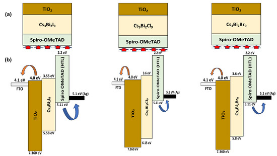
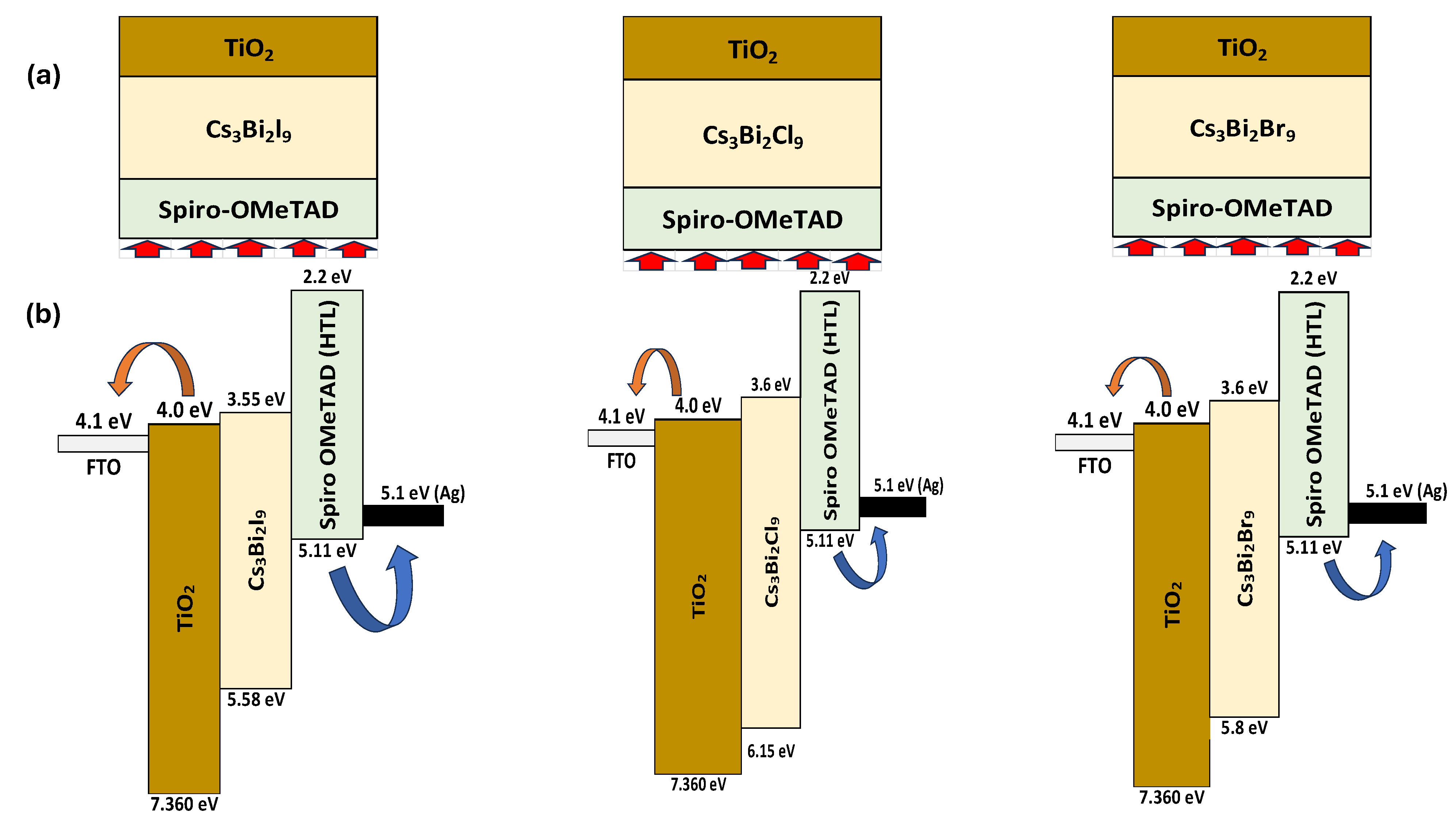
Figure 1a,b presents the device representation of our three inverted perovskite structures along with their proposed band gap alignment diagram. The parametric values for all perovskite, charge-transporting layers, and interfacing layers were obtained from reputable literature sources and are listed in Table 1 and Table 2 [27,28,29,30,31,32,33,34,35,36], as discussed earlier. The thermal velocities of electrons and holes were standardized at 107 cm/s. The absorption coefficient values for all perovskite and charge-transporting layers utilized the default standardized built-in values from SCAPS-1D. The absorption coefficient values of SCAPS-1D were determined using a prominent mathematical equation for absorption coefficients, as presented below [37]:
Figure 1.
(a) Diagram of all three perovskite devices and (b) band gap alignment of perovskite structures.
In the equation above, A and B are arbitrary constants; h represents Planck’s constant; ν denotes the optical frequency of photons; and Eg signifies the band gap energy of perovskite materials. The thickness and doping concentrations of perovskite and other charge-transporting layer parameters were utilized in the initial stage without optimization.
3. Results and Discussion
3.1. Electrical J-V and Optical QE (%) Analysis for Perovskite Devices
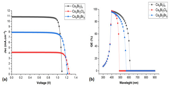
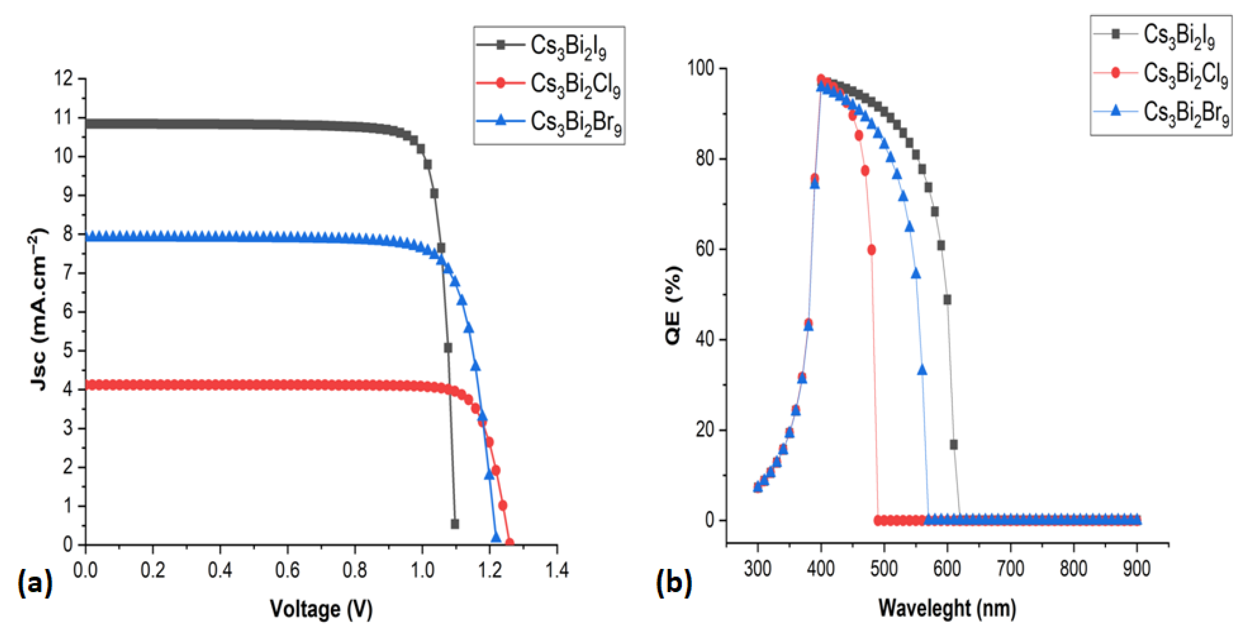
The electrical and optical characteristics of the perovskite photovoltaic devices were examined via J-V and QE methodologies under standardized testing settings. The device architecture, characterized by the layer configuration of FTO Glass (400 nm)/TiO2 (50 nm)/Perovskite (500 nm)/Spiro-OMeTAD (500 nm), was simulated utilizing the parameters specified in Table 1 and Table 2. The performance parameters obtained from device simulations are listed in Table 3, while the graphical representations of the J-V and QE analyses are shown in Figure 2. Cs3Bi2I9 exhibited the highest performance parameters, achieving a power conversion efficiency of up to 10.01%, open-circuit voltage of 1.08 V, short-circuit current of 10.84 mA.cm−2, and fill factor of 85.37%. In contrast, Cs3Bi2I9-based perovskite demonstrated intermediate performance with a power conversion efficiency of up to 7.56%, open-circuit voltage of 1.20 V, short-circuit current of 7.91 mA.cm−2, and fill factor of 79.50%. Cs3Bi2Cl9 showed the lowest performance parameters, with a power conversion efficiency of up to 4.34%, open-circuit voltage of 1.26 V, short-circuit current of 4.12 mA.cm−2, and fill factor of 83.50%. The Cs3Bi2Cl9 perovskite exhibited distinct behaviour at a higher open-circuit voltage of 1.26 V compared to the other two devices, although other performance parameters were significantly degraded. The higher short-circuit current value of the Cs3Bi2I9-based device is attributed to lower recombination currents in comparison to the other two perovskite devices [38]. A comparable trend was observed in the fill factor value for the Cs3Bi2I9-based device, attributed to reduced series resistance and recombination rates [39]. The performance parameters of all devices were calculated without optimizing thickness, doping concentrations, and layer defects. The optimized results, along with graphical representations, are presented in the subsequent section. The analysis of optical properties indicated a similar trend across the visible light spectrum from 300 nm to 900 nm (Cs3Bi2I9 > Cs3Bi2Br9 > Cs3Bi2Cl9). The quantum efficiency of Cs3Bi2I9 indicates superior absorption capability and enhanced charge carrier generation across the light spectrum, resulting in improved performance parameters relative to other Cs-based perovskite devices [40].
Table 3.
J-V characteristic (performance parameters) for all perovskite devices.
Figure 2.
(a) Graphical representation of J-V analysis (electrical) for perovskite devices and (b) QE (%) analysis of all Cs-based perovskite devices.
The higher quantum efficiency value of the Cs3Bi2I9-based perovskite device also justifies our electrical analysis results and performance parameters. The tentative comparison between all Cs-based perovskite devices can be analyzed from Table 3.
Based on our best investigation, we concluded that Cs3Bi2Cl9 had the lowest QE (%) against the light spectrum between 300 and 900 nm, which resulted in poor performance characteristics and absorption. This performance degradation is attributed to inadequate surface morphology, increased surface defects, reduced carrier lifetime, and carrier diffusion issues [41].
3.2. Impact of Hole-Transport Layer Thickness Variation on Performance Parameters of Devices
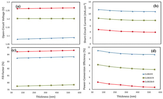
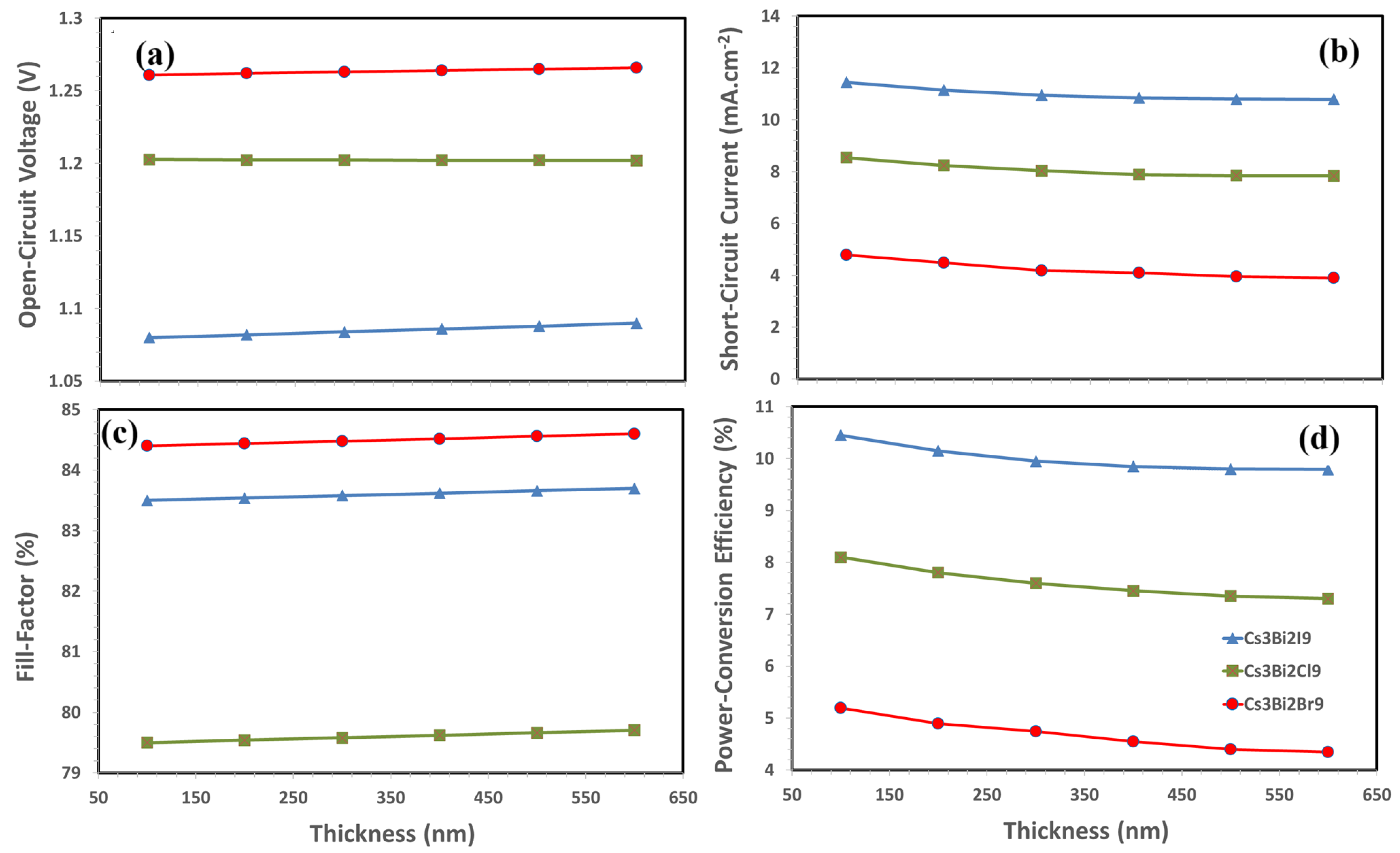
The thickness of the hole-transport layer was varied from 100 nm to 600 nm to assess its effect on the performance parameters of all three perovskite devices, while maintaining constant values for other parameters in the simulation analysis. The results are shown in Figure 3. No significant changes in open-circuit voltage were observed with variations in hole-transport layer thickness across all devices, exhibiting behaviour similar to that of short-circuit, see Figure 3a,b. In the case of short-circuit current, degradation was observed with variations in the thickness of the hole-transport layer ranging from 100 nm to 600 nm. The decline in short-circuit current was linked to increased recombination currents; as the thickness of the hole-transport layer increased, the devices experienced elevated recombination rates and diminished charge carrier mobility towards the electrode [42,43,44]. In the case of fill factor (see Figure 3c), a minor degradation was observed with variations in the thickness of the hole-transport layer for all perovskite devices, attributed to increased series resistance associated with greater hole-transport layer thickness [45,46]. The PCE (See Figure 3d) of all devices decreased as a result of the decline in short-circuit current and fill factor values with increased thickness of the hole-transport layer for Cs3Bi2I9 (10.41% to 9.84%), Cs3Bi2Br9 (8.09% to 7.50%), and Cs3Bi2Cl9 (4.93% to 4.27%), respectively. Figure 3 illustrates the graphical representations of the variation in thickness of the hole-transport layer on the performance parameters for all three perovskite devices. The optimized thickness value was determined to be 100 nm for all perovskite structures based on simulation results [47].
Figure 3.
Effect of thickness variation in hole-transport layer on performance of perovskite devices: (a) open-circuit voltage, (b) short-circuit current, (c) fill factor, and (d) power conversion efficiency.
3.3. Impact of Thickness of Electron-Transport Layer on Performance Parameter of Cs-Based Perovskite
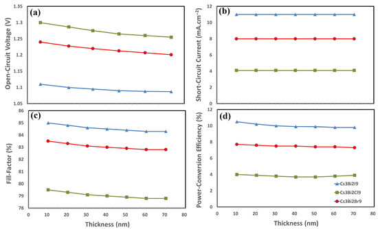
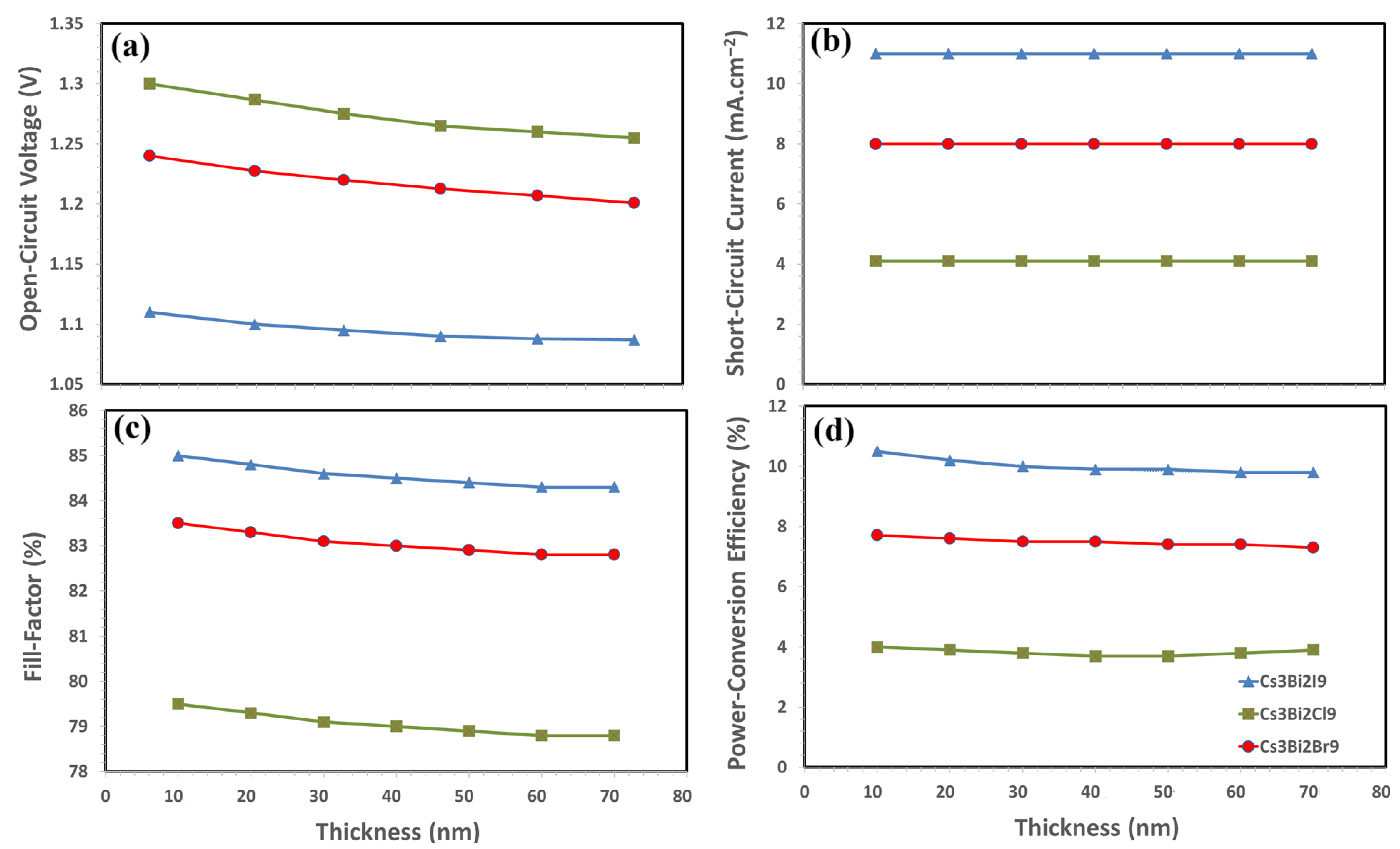
The thickness of the electron-transport layer significantly influences the performance parameters of a specific perovskite device. The electron-transport layer thickness of all perovskite samples ranged from 10 nm to 70 nm, and performance parameters were subsequently analyzed. It was observed that as the thickness of the electron-transport layer increased, the values of open-circuit voltage for all devices tended to degrade significantly. We attributed these open-circuit voltage losses to inadequate diffusion lengths and the limited carrier extraction capability of charge carriers at the tentative electrode [48,49,50]. Surprisingly, no significant degradation was observed in short-circuit current with respect to the variation in electron-transport layer thickness across all perovskite devices. Similar degradation was observed in terms of fill factor (%), with consistent degradation noted as the thickness of the electron-transport layer increased. The consistent degradation was attributed to increased series resistance, which further leads to elevated recombination rates in perovskite structures [51]. The power conversion efficiency of perovskite devices is primarily influenced by the open-circuit voltage, fill factor, and short-circuit current density. The ultimate power conversion efficiency decreased from 10.31% to 9.89% for Cs3Bi2I9, from 7.84% to 7.55% for Cs3Bi2Br9, and from 4.46% to 4.31% for Cs3Bi2Cl9. Figure 4 presents graphical representations for three perovskite devices. Our simulation analysis indicates that the optimized thickness for the electron-transport layer in all devices is approximately 10 nm, which demonstrates superior performance parameters across varying thicknesses.
Figure 4.
Effect of thickness variation in electron-transport layer on performance of perovskite devices: (a) open-circuit voltage, (b) short-circuit current, (c) fill factor, and (d) power conversion efficiency.
3.4. Impact of Acceptor Density of Hole-Transport Layer on Performance Parameters
To assess the overall impact of acceptor density in the hole-transport layer on all perovskite devices, we varied its value from 1015 cm−3 to 1020 cm−3 at the logarithmic scale, while maintaining constant values for other structural parameters. Simulation results were subsequently computed. The simulation results and the effect of varying acceptor density in the hole-transport layer on performance parameters are presented in Figure 5a–d. We observed a slight increase in open-circuit voltage values, as shown in Figure 5a for Cs3Bi2I9, while the open-circuit voltage values for Cs3Bi2Cl9 initially increase and then become constant. In contrast, Cs3Bi2Br9 exhibited a more significant increase with variations in the acceptor density of the hole-transport layer. This improvement in open-circuit voltage for Cs3Bi2Br9 is attributed to the enhanced electric field at the hole-transport layer/perovskite interface, which facilitates greater charge accumulation or extraction from the absorber layer, resulting in a lower dark saturation current [52,53]. No significant changes were observed in the short-circuit current with respect to variations in acceptor density of the hole-transport layer across all devices, see Figure 5b. Our observations indicate significant improvement in the variation in acceptor density of the hole-transport layer for fill factor (%) across all devices, as shown in Figure 5c, which may contribute to the reduction of overall series resistances (layers and metal contacts) in the devices [54]. The observed enhancement was consistent across the devices, leading to tentative improvements in the power conversion efficiency values for all structures (Figure 5d): Cs3Bi2I9 (8.94% to 10.14%), Cs3Bi2Cl9 (3.85% to 5.04%), and Cs3Bi2Br9 (6.59% to 8.74%). Our observations indicate that the optimized acceptor density for the hole-transport layer in all perovskite structures is approximately 1020 cm−3. This value demonstrates significant improvements compared to the control doping concentration of 1018 cm−3. When the doping concentration in the hole-transport layer reached 1020 cm−3, higher performance was observed. However, further increases in acceptor density may result in reduced hole mobility due to the generation of deep Coulomb trap states [55,56]. Figure 5 illustrates the impact of varying doping concentration on the performance parameters of the devices.
Figure 5.
Effect of acceptor density NA (cm−3) of hole-transport layer on performance parameters of all perovskite devices: (a) open-circuit voltage, (b) short-circuit current, (c) fill factor, and (d) and power conversion efficiency.
3.5. Impact of Donor Density Variation ND (cm−3) of Electron-Transport Layer on Performance Parameters
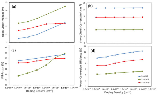
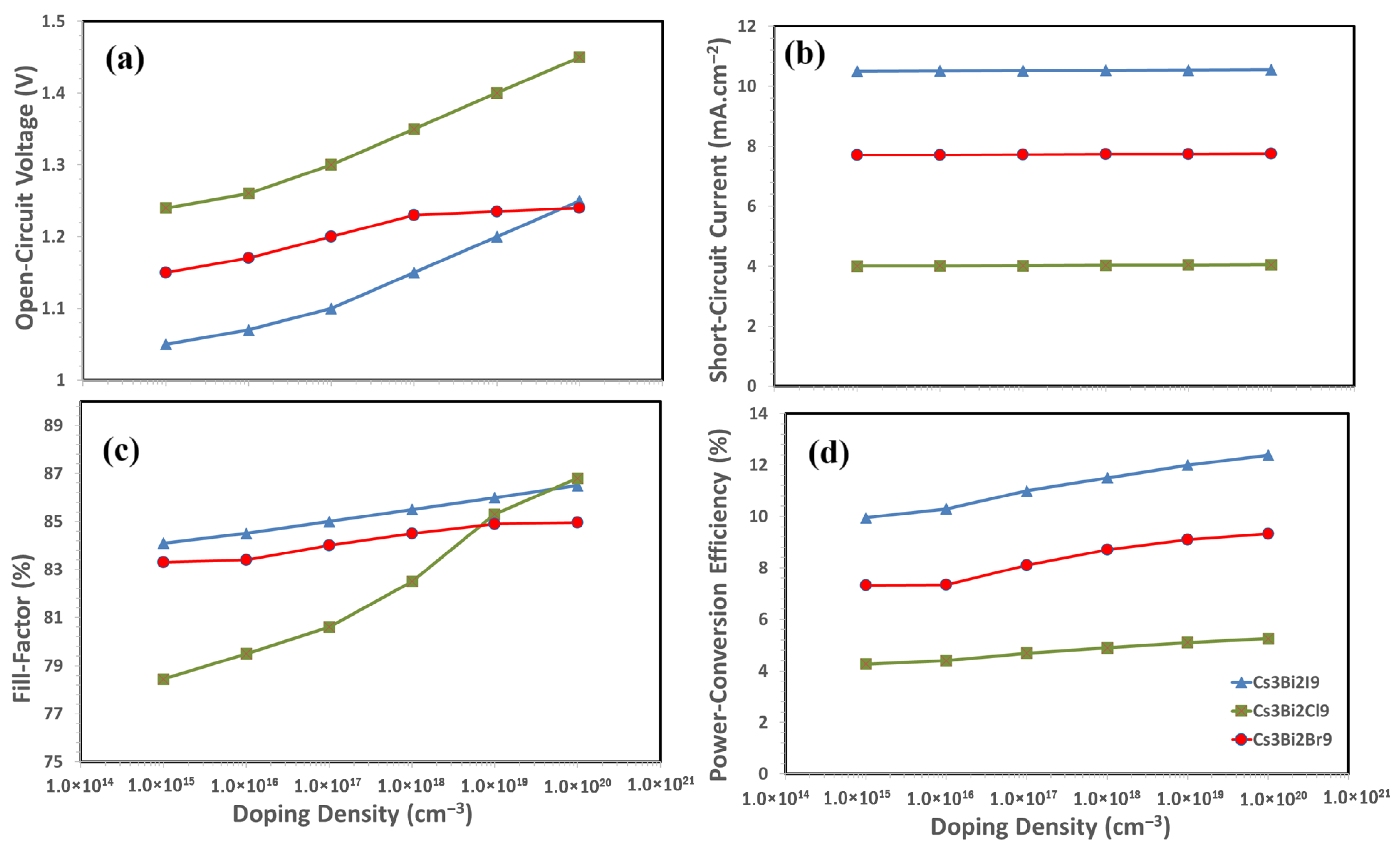
The acceptor density of the electron-transport layer was varied from 1015 cm−3 to 1020 cm−3 on a logarithmic scale to assess its impact on the performance of all three perovskite structures, as shown in Figure 6a–d. The performance parameters, excluding short-circuit current (see Figure 6b), of all devices improved with increased donor density of the electron-transport layer [57,58]. The open-circuit voltage increased for all devices as a function of electron-transport layer doping density, respectively. A similar trend was observed regarding FF improvements, attributed to increased doping concentration in the electron-transport layer, which tentatively enhanced FF values for all perovskite structures by reducing series resistance (layers and interface) in perovskite devices. Additionally, a significant electric field was established at the perovskite/electron-transport layer interface, which likely inhibited interfacial recombination and altered the movement of charge carriers towards the electrodes [59,60]. The enhancements in open-circuit voltage (see Figure 6a) and fill factor (see Figure 6c) values resulting from increased donor concentration in the electron-transport layer tentatively elevated the PCE (see Figure 6d) of all structures: from 9.95% to 12.39% for Cs3Bi2I9, from 4.27% to 5.25% for Cs3Bi2Cl9, and from 7.32% to 9.32% for Cs3Bi2Br9. Simulation results indicated that a doping concentration of 1020 cm−3 in the electron-transport layer was optimized, leading to improved performance parameters for all perovskite devices [61,62]. Figure 6 illustrates the relationship between the doping (donor) concentration of the electron-transport layer and the performance parameters, including open-circuit voltage, short-circuit current, fill factor, and power conversion efficiency.
Figure 6.
Representational effect of donor density (ND cm−3) of electron-transport layer on performance parameters of all perovskite devices: (a) open-circuit voltage, (b) short-circuit current, (c) fill factor, and (d) power conversion efficiency.
3.6. Impact of Doping Concentration ND (cm−3) of Absorber Layer on Performance Parameters of Devices
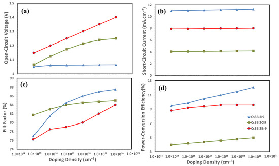
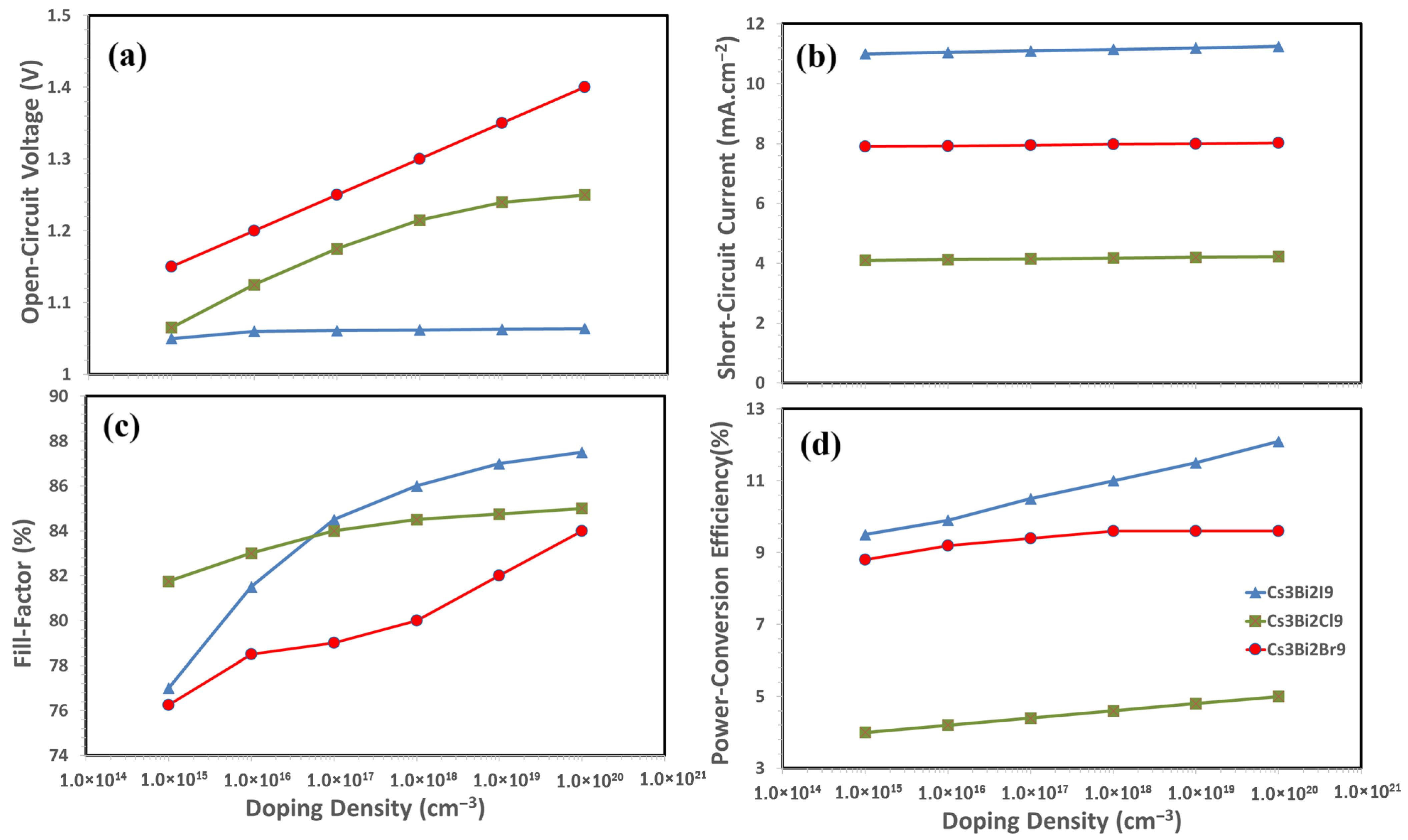
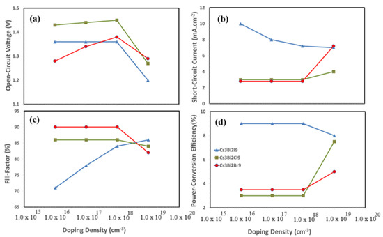
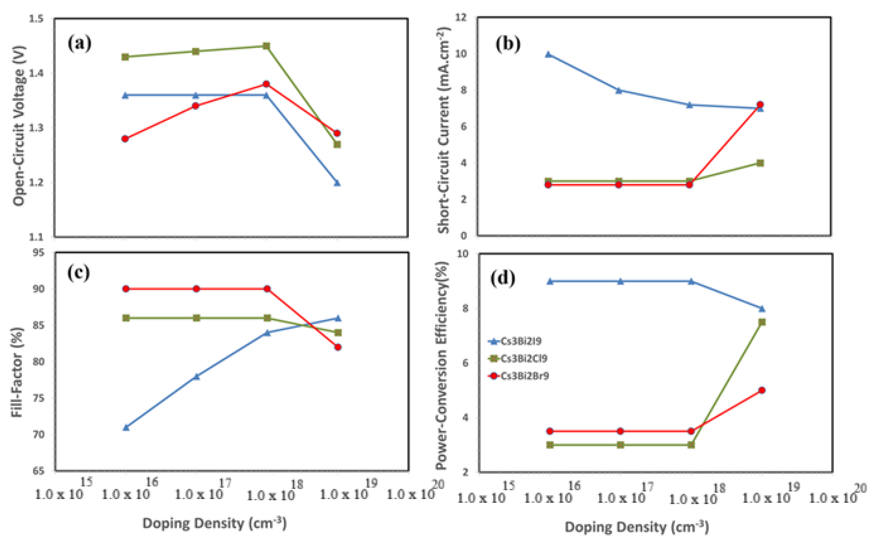
The doping concentration of the absorber layer is crucial for enhancing device performance. Consequently, we simulated the proposed perovskite structures while varying the doping concentration of the absorber layer from 1016 cm−3 to 1019 cm−3, and we computed the corresponding performance parameters. The results are shown in Figure 7a–d. We observed that increasing the doping concentrations of the absorber led to a degradation in the open-circuit voltage values of all devices (Figure 7a). The increased open-circuit voltage losses were attributed to a greater number of vacancy defects resulting from variations in deep doping concentration within the absorber layer of all devices [63]. Literature studies indicate that vacancy defects can alter the nature of the absorber layer from n-type to p-type as doping concentration increases, establishing a direct relationship between vacancy defects and open-circuit voltage losses [64,65]. The decline in open-circuit voltage associated with increased doping concentration in absorber layers can be explained using the following mathematical equation:
Figure 7.
Representational effect of donor density (ND cm−3) of Absorber layers on performance parameters of all perovskite devices: (a) open-circuit voltage, (b) short-circuit current, (c) fill factor, and (d) and power conversion efficiency.
In the equation presented above, n represents the ideality factor, VT denotes the thermal voltage, I0 signifies the dark saturation current, and IG indicates the light-generated current. An increase in doping concentration results in a corresponding rise in dark saturation current, which, according to the equation, leads to a degradation of open-circuit voltage. A similar trend was observed in the short-circuit current (Figure 7b) degradation of Cs3Bi2I9 with varying doping concentrations, indicating a general mechanism. However, the other two devices, Cs3Bi2Cl9 and Cs3Bi2Br9, exhibited atypical behaviour, as short-circuit current values improved with changes in doping concentration, representing a special case. The fill factor values of Cs3Bi2Cl9 and Cs3Bi2Br9 (see Figure 7c) tended to degrade with increasing doping concentration within both absorber layers due to the transformation from n-type to p-type, also referred to as vacancy defects. The overall PCE for Cs3Bi2Cl9 and Cs3Bi2Br9 improved, whereas Cs3Bi2I9 exhibited degradation at higher doping concentrations, indicating a generalized trend. The graphical representation of these performance parameters is provided in Figure 7. Our calculations indicate a recommended doping concentration of 1019 cm−3 for Cs3Bi2Cl9 and Cs3Bi2Br9, and 1016 cm−3 for Cs3Bi2I9.
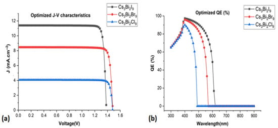
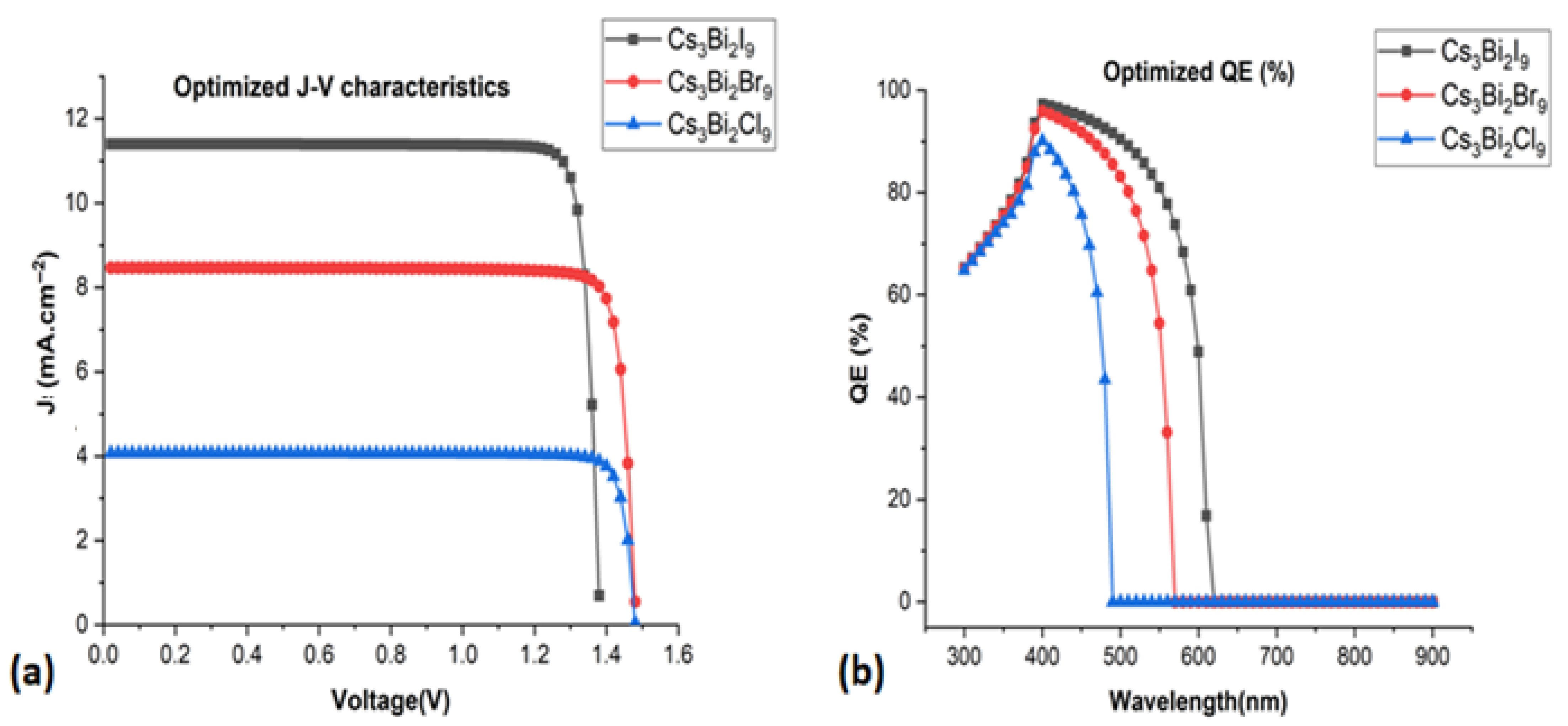
The power conversion efficiency (see Figure 8a) of Cs3Bi2I9 increased from 10.01% to 14.08% following parameter optimization, while Cs3Bi2Cl9 improved from 4.34% to 5.28%, and Cs3Bi2Br9 rose from 7.56% to 11.05%. The optimized performance parameters of perovskite devices, as shown in Table 4, demonstrate that all devices exhibited superior performance relative to the initial unoptimized perovskite structure. Similar improvements were observed in the J-V curve and QE, indicating that the optical and electrical properties have been altered compared to unoptimized perovskite structures.
Figure 8.
Graphical representation of performance optimization for all the perovskite devices, (a) Optimized J-V characteristic curve, (b) Optimized QE for the devices.
Table 4.
Optimized Performance Parameters for all the perovskite devices.
4. Conclusions
A comparative investigation of the performance of three cesium-based perovskite solar cells (Cs3Bi2I9, Cs3Bi2Cl9, and Cs3Bi2Br9) was performed using a series of simulations. In this study, three inverted perovskite structures were proposed for simulations and performance optimization analysis: FTO/Spiro-OMeTAD/Cs3Bi2I9/TiO2, FTO/Spiro-OMeTAD/Cs3Bi2Cl9/TiO2, and FTO/Spiro-OMeTAD/Cs3Bi2Br9/TiO2. Parametric optimization for perovskite devices is essential for enhancing performance and achieving improvements. In our simulation and modelling, we varied key layer parameters, including the thickness of charge-transport layers, absorber layers, and the doping concentrations of electron-transport layers, hole-transport layers, and all three absorber layers, to enhance device performance. A significant enhancement in PCE values was observed for all three perovskite structures when compared to unoptimized configurations. The power conversion efficiencies increased from 10.01% to 14.08% for Cs3Bi2I9, from 4.34% to 5.28% for Cs3Bi2Cl9, and from 7.56% to 11.05% for Cs3Bi2Br9. The optical properties were enhanced across the visible spectrum following the optimization of the parametric values for all devices. Cs3Bi2I9 exhibited superior performance in terms of power conversion efficiency and quantum efficiency values relative to the other two Cs-based perovskite devices. The comparison of the electrical and optical performances of perovskite devices, following parametric optimization, reveals the following trend: Cs3Bi2I9 > Cs3Bi2Br9 > Cs3Bi2Cl9. This study’s concept and simulation analysis may significantly aid in the design of environmentally friendly perovskite solar cells, in contrast to toxic Pb-based perovskite alternatives. This work represents a significant advancement in the design of environmentally friendly and cost-effective perovskite, with implications for both theoretical and laboratory research in the future.
Author Contributions
M.A.: Conceptualization, Methodology, Software, Validation, Formal Analysis, Investigation, Data Curation, and Writing—Original Draft and Visualization. S.A.M.: Supervision, Project Administration, Resources, and Writing—Review and Editing. A.N.M.A.: Supervision and Writing—Review and Editing. M.S.A.: Supervision and Writing—Review and Editing. All authors have read and agreed to the published version of the manuscript.
Funding
This research work was funded by Umm Al-Qura University, Saudi Arabia under grant number: 25UQU4330024GSSR02.
Institutional Review Board Statement
Not applicable.
Informed Consent Statement
Not applicable.
Data Availability Statement
The original contributions presented in this study are included in the article. Further inquiries can be directed to the corresponding author.
Acknowledgments
The authors extend their appreciation to Umm Al-Qura University, Saudi Arabia for funding this research work through grant number: 25UQU4330024GSSR02.
Conflicts of Interest
The authors declare no conflicts of interest.
References
- Gyamfi, B.A.; Adebayo, T.S.; Agozie, D.Q.; Bekun, F.V.; Koy, A. Is sustainable energy consumption, technological advancement and urbanization fast addressing south Asia’s green energy expansion deficits? Environ. Dev. Sustain. 2025, 27, 19969–19998. [Google Scholar] [CrossRef] [Scilit]
- Reddy, A.K.; Goldemberg, J. Energy for the developing world. Sci. Am. 1990, 263, 110–119. [Google Scholar] [CrossRef] [Scilit]
- Holdren, J.P. Population and the energy problem. Popul. Environ. 1991, 12, 231–255. [Google Scholar] [CrossRef] [Scilit]
- Rice, M.B.; Thurston, G.D.; Balmes, J.R.; Pinkerton, K.E. Climate change. A global threat to cardiopulmonary health. Am. J. Respir. Crit. Care Med. 2014, 189, 512–519. [Google Scholar] [CrossRef] [Scilit]
- Moiz, S.A.; Alshaikh, M.S.; Alahmadi, A.N. Organic Bioelectronics: Diversity of Electronics Along with Biosciences. Biosensors 2025, 15, 587. [Google Scholar] [CrossRef] [Scilit]
- Yang, C.; Hu, W.; Liu, J.; Han, C.; Gao, Q.; Mei, A.; Zhou, Y.; Guo, F.; Han, H. Achievements, challenges, and future prospects for industrialization of perovskite solar cells. Light Sci. Appl. 2024, 13, 227. [Google Scholar] [CrossRef] [Scilit]
- Nazir, G.; Lee, S.Y.; Lee, J.H.; Rehman, A.; Lee, J.K.; Seok, S.I.; Park, S.J. Stabilization of perovskite solar cells: Recent developments and future perspectives. Adv. Mater. 2022, 34, 2204380. [Google Scholar] [CrossRef] [Scilit]
- Akkerman, Q.A.; Manna, L. What defines a halide perovskite? ACS Energy Lett. 2020, 5, 604–610. [Google Scholar] [CrossRef] [Scilit]
- Lee, Y.H.; Luo, J.; Son, M.-K.; Gao, P.; Cho, K.T.; Seo, J.; Zakeeruddin, S.M.; Grätzel, M.; Nazeeruddin, M.K. Enhanced Charge Collection with Passivation Layers in Perovskite Solar Cells. Adv. Mater. 2016, 28, 3966–3972. [Google Scholar] [CrossRef] [Scilit]
- Jošt, M.; Kegelmann, L.; Korte, L.; Albrecht, S. Monolithic Perovskite Tandem Solar Cells: A Review of the Present Status and Advanced Characterization Methods Toward 30% Efficiency. Adv. Energy Mater. 2020, 10, 1904102. [Google Scholar] [CrossRef] [Scilit]
- Moiz, S.A.; Alahmadi, A.N.; Alshaikh, M.S. Design Optimization of Cesium Contents for Mixed Cation MA1− xCsxPbI3-Based Efficient Perovskite Solar Cell. Nanomaterials 2025, 15, 1085. [Google Scholar] [CrossRef] [Scilit]
- Yang, M.; Bai, Y.; Meng, Y.; Tian, R.; Sun, K.; Lu, X.; Pan, H.; Wang, J.; Zhou, S.; Zhang, J.; et al. Sn-Pb Perovskite with Strong Light and Oxygen Stability for All-Perovskite Tandem Solar Cells. Adv. Mater. 2025, 37, 2415627. [Google Scholar] [CrossRef] [Scilit]
- Sun, Y.; Lai, Y.; Yang, Y. Progress of Hole-Transport Layers in Mixed Sn-Pb Perovskite Solar Cells. Small 2024, 20, 2406991. [Google Scholar] [CrossRef] [Scilit] [PubMed]
- Li, B.; Chang, B.; Pan, L.; Li, Z.; Fu, L.; He, Z.; Yin, L. Tin-based defects and passivation strategies in tin-related perovskite solar cells. ACS Energy Lett. 2020, 5, 3752–3772. [Google Scholar] [CrossRef] [Scilit]
- Cao, F.; Bian, L.; Li, L. Perovskite solar cells with high-efficiency exceeding 25%: A review. Energy Mater. Devices 2024, 2, 9370018. [Google Scholar] [CrossRef] [Scilit]
- Lanzetta, L.; Webb, T.; Zibouche, N.; Liang, X.; Ding, D.; Min, G.; Westbrook, R.J.E.; Gaggio, B.; Macdonald, T.J.; Islam, M.S.; et al. Degradation mechanism of hybrid tin-based perovskite solar cells and the critical role of tin (IV) iodide. Nat. Commun. 2021, 12, 2853. [Google Scholar] [CrossRef] [Scilit]
- Al-Anesi, B.; Grandhi, G.K.; Pecoraro, A.; Sugathan, V.; Viswanath, N.S.M.; Ali-Löytty, H.; Liu, M.; Ruoko, T.; Lahtonen, K.; Manna, D.; et al. Antimony-Bismuth Alloying: The Key to a Major Boost in the Efficiency of Lead-Free Perovskite-Inspired Photovoltaics. Small 2023, 19, 2303575. [Google Scholar] [CrossRef] [Scilit]
- Vargas, B.; Coutiño-Gonzalez, E.; Ovalle-Encinia, O.; Sánchez-Aké, C.; Solis-Ibarra, D. Efficient Emission in Halide Layered Double Perovskites: The Role of Sb3+ Substitution in Cs4Cd1–x Mn x Bi2Cl12 Phosphors. J. Phys. Chem. Lett. 2020, 11, 10362–10367. [Google Scholar] [CrossRef] [Scilit]
- Arfin, H.; Kshirsagar, A.S.; Kaur, J.; Mondal, B.; Xia, Z.; Chakraborty, S.; Nag, A. ns2 electron (Bi3+ and Sb3+) doping in lead-free metal halide perovskite derivatives. Chem. Mater. 2020, 32, 10255–10267. [Google Scholar] [CrossRef] [Scilit]
- Chen, X.; Jia, M.; Xu, W.; Pan, G.; Zhu, J.; Tian, Y.; Wu, D.; Li, X.; Shi, Z. Recent progress and challenges of bismuth-based halide perovskites for emerging optoelectronic applications. Adv. Opt. Mater. 2023, 11, 2202153. [Google Scholar] [CrossRef] [Scilit]
- Wang, J.; Li, Y.; Ma, L.; Shen, G.; Yang, Q. Air-Stabilized Lead-Free Hexagonal Cs3Bi2I9 Nanocrystals for Ultrahigh-Performance Optical Detection. Adv. Funct. Mater. 2022, 32, 2203072. [Google Scholar] [CrossRef] [Scilit]
- Ghosh, B.; Wu, B.; Mulmudi, H.K.; Guet, C.; Weber, K.; Sum, T.C.; Mhaisalkar, S.; Mathews, N. Limitations of Cs3Bi2I9 as lead-free photovoltaic absorber materials. ACS Appl. Mater. Interfaces 2018, 10, 35000–35007. [Google Scholar] [CrossRef] [Scilit]
- Verschraegen, J.; Burgelman, M. Numerical modeling of intra-band tunneling for heterojunction solar cells in scaps. Thin Solid Film. 2007, 515, 6276–6279. [Google Scholar] [CrossRef] [Scilit]
- Moiz, S.A.; Alzahrani, M.S.; Alahmadi, A.N. Electron transport layer optimization for efficient PTB7: PC70BM bulk-heterojunction solar cells. Polymers 2022, 14, 3610. [Google Scholar] [CrossRef] [Scilit]
- Moiz, S.A.; Alahmadi, A.N.; Alshaikh, M.S. Lead-free FACsSnI3 based perovskite solar cell: Designing hole and electron transport layer. Nanomaterials 2023, 13, 1524. [Google Scholar] [CrossRef] [Scilit] [PubMed]
- Pindolia, G.; Shinde, S.M.; Jha, P.K. Optimization of an inorganic lead free RbGeI3 based perovskite solar cell by SCAPS-1D simulation. Sol. Energy 2022, 236, 802–821. [Google Scholar] [CrossRef] [Scilit]
- Moiz, S.A.; Alahmadi, A.N.M.; Aljohani, A.J. Design of a novel lead-free perovskite solar cell for 17.83% efficiency. IEEE Access 2021, 9, 54254–54263. [Google Scholar] [CrossRef] [Scilit]
- Karthick, S.; Velumani, S.; Bouclé, J. Chalcogenide BaZrS3 perovskite solar cells: A numerical simulation and analysis using SCAPS-1D. Opt. Mater. 2022, 126, 112250. [Google Scholar] [CrossRef] [Scilit]
- Islam, T.; Jani, R.; Shorowordi, K.M.; Hoque, Z.; Gokcek, A.M.; Vattipally, V.; Nishat, S.S.; Ahmed, S. Numerical simulation studies of Cs3Bi2I9 perovskite solar device with optimal selection of electron and hole transport layers. Optik 2021, 231, 166417. [Google Scholar] [CrossRef] [Scilit]
- Kim, S.Y.; Park, D.A.; Park, N.G. Synthetic powder-based thin (<0.1 μm) Cs3Bi2Br9 perovskite films for air-stable and viable resistive switching memory. ACS Appl. Electron. Mater. 2022, 4, 2388–2395. [Google Scholar]
- Tailor, N.K.; Satapathi, S. The impact of Cs3Bi2Cl9 single crystal growth modality on its symmetry and morphology. J. Mater. Res. Technol. 2020, 9, 7149–7157. [Google Scholar] [CrossRef] [Scilit]
- Hock, R.; Mayer, T.; Jaegermann, W. P-type doping of spiro-MeOTAD with WO3 and the spiro-MeOTAD/WO3 interface investigated by synchrotron-induced photoelectron spectroscopy. J. Phys. Chem. C 2012, 116, 18146–18154. [Google Scholar] [CrossRef] [Scilit]
- Fellmeth, T.; Clement, F.; Biro, D. Analytical modeling of industrial-related silicon solar cells. IEEE J. Photovolt. 2013, 4, 504–513. [Google Scholar] [CrossRef] [Scilit]
- Rombach, F.M.; Haque, S.A.; Macdonald, T.J. Lessons learned from spiro-OMeTAD and PTAA in perovskite solar cells. Energy Environ. Sci. 2021, 14, 5161–5190. [Google Scholar] [CrossRef] [Scilit]
- Moiz, S.A.; Masud, M.I. Enhancing CaV0.5Fe0.5O3-Based Lead-Free Perovskite Solar Cell Efficiency by over 23% via Transport Layer Engineering. Nanomaterials 2025, 15, 1646. [Google Scholar] [CrossRef] [Scilit] [PubMed]
- Moiz, S.A.; Alshaikh, M.S.; Alahmadi, A.N. Simulation design of novel non-fluorine polymers as electron transport layer for lead-free Perovskite solar cells. Polymers 2023, 15, 4387. [Google Scholar] [CrossRef] [Scilit]
- Burgelman, M.; Decock, K.; Niemegeers, A.; Verschraegen, J.; Degrave, S. SCAPS Manual; University of Ghent: Ghent, Belgium, 2016. [Google Scholar]
- Ataei, M.; Adelifard, M.; Hosseini, S.S. Physical properties and photovoltaic performance of perovskite solar cells based on lead-free A3Bi2I9 (A= CH3NH3, Cs) active layers. J. Electron. Mater. 2021, 50, 571–579. [Google Scholar] [CrossRef] [Scilit]
- Toki, G.F.I.; Hossain, M.K.; Pandey, R.; Bhattarai, S.; Tawfeek, A.M.; Mohammad, S.; Habib, A.M.J.; Mahmud, N.; Rahman, F.; Sasikumar, P.; et al. Optimizing lead-free Cs3Bi2I9 perovskite solar cells: Exploring absorber and charge transport layers parameters for improved efficiency. J. Opt. 2024, 53, 4554–4570. [Google Scholar] [CrossRef] [Scilit]
- Jokar, E.; Chien, C.H.; Tsai, C.M.; Fathi, A.; Diau, E.W.G. Robust tin-based perovskite solar cells with hybrid organic cations to attain efficiency approaching 10%. Adv. Mater. 2019, 31, 1804835. [Google Scholar] [CrossRef] [Scilit]
- Vandewal, K.; Ma, Z.; Bergqvist, J.; Tang, Z.; Wang, E.; Henriksson, P.; Tvingstedt, K.; Andersson, M.R.; Zhang, F.; Inganäs, O. Quantification of Quantum efficiency and energy losses in low bandgap polymer: Fullerene solar cells with high open-circuit voltage. Adv. Funct. Mater. 2012, 22, 3480–3490. [Google Scholar] [CrossRef] [Scilit]
- Zhou, X.; Han, J. Design and simulation of C2N based solar cell by SCAPS-1D software. Mater. Res. Express 2020, 7, 126303. [Google Scholar] [CrossRef] [Scilit]
- Moiz, S.A.; Jee, S.W.; Um, H.D.; Lee, J.H. Electrical characterization of metal–silicon microwire interface using conductive atomic force microscope. Jpn. J. Appl. Phys. 2010, 49, 045003. [Google Scholar] [CrossRef] [Scilit]
- Tumusange, M.S.; Chen, L.; Mainali, M.K.; Frye, B.M.; Amonette, E.J.; Bordovalos, A.V.; Song, Z.; Yan, Y.; Podraza, N.J. Monitoring degradation and carrier collection losses of narrow bandgap perovskite solar cells with different organic hole transport layers by spectroscopic ellipsometry and external quantum efficiency. Sol. Energy 2025, 288, 113243. [Google Scholar] [CrossRef] [Scilit]
- Kim, G.W.; Shinde, D.V.; Park, T. Thickness of the hole transport layer in perovskite solar cells: Performance versus reproducibility. RSC Adv. 2015, 5, 99356–99360. [Google Scholar] [CrossRef] [Scilit]
- Mudassar, M.M.; Arshad, M.; Salman, M.U.; Mahmood, A.; Al-Masry, W.; Asim, M.; Atiq, S. Significance of the direct relation between the fill factor and hole transport layer thickness in perovskite-based solar cells for green energies. RSC Adv. 2025, 15, 33830–33843. [Google Scholar] [CrossRef] [Scilit] [PubMed]
- Du, T.; Xu, W.; Xu, S.; Ratnasingham, S.R.; Lin, C.T.; Kim, J.; Briscoe, J.; McLachlan, M.A.; Durrant, J.R. Light-intensity and thickness dependent efficiency of planar perovskite solar cells: Charge recombination versus extraction. J. Mater. Chem. C 2020, 8, 12648–12655. [Google Scholar] [CrossRef] [Scilit]
- Raoui, Y.; Ez-Zahraouy, H.; Tahiri, N.; El Bounagui, O.; Ahmad, S.; Kazim, S. Performance analysis of MAPbI3 based perovskite solar cells employing diverse charge selective contacts: Simulation study. Sol. Energy 2019, 193, 948–955. [Google Scholar] [CrossRef] [Scilit]
- Li, Z.; Xie, X.; Ai, Z.; Han, Y.; Zhu, T.; Ma, R.; Liu, H.; Lu, X.; Wei, Q.; Li, M.; et al. Electron Extraction Optimization for Carbon-Based Hole-Conductor-Free Perovskite Photovoltaics with Record 1.41 V VOC. Adv. Mater. 2025, 37, 2502436. [Google Scholar] [CrossRef] [Scilit]
- Karimov, K.S.; Moiz, S.A.; Tahir, M.M.; Ahmed, N.; Tariq, R.; Abbas, S.Z.; Zafar, Q. Nickel phthalocynanine-metal Schottky diode as photodetector. J. Optoelectron. Adv. Mater. 2014, 16, 1430–1435. [Google Scholar]
- Chen, J.; Park, N.G. Causes and solutions of recombination in perovskite solar cells. Adv. Mater. 2019, 31, 1803019. [Google Scholar] [CrossRef] [Scilit]
- Zhao, X.-Y.; Zhang, X.-S.; Liu, X.; Gong, X.-K.; Yuan, X.-R.; Zhou, B.-Z.; Xu, J.-P.; Kong, L.-N.; Li, L. Improving efficiency of silicon solar cells by integrating SiO2-coated lead-free Cs3Bi2Br9 perovskites quantum dots as luminescence down-shifting layer. Colloids Surf. A Physicochem. Eng. Asp. 2024, 682, 132887. [Google Scholar] [CrossRef] [Scilit]
- Jayawardane, S.T.; Akmal, M.D.; Jayaneththi, Y.H.; Fernando, T.V.; Hu, D.; Abeygunawardhana, P.K.; Sewvandi, G.A. Simulation-based performance analysis of lead-free bismuth perovskite solar cells: A comparative study of Cs3Bi2I9 and (CH3NH3) 3Bi2I9-based perovskite solar cells. Adv. Theory Simul. 2024, 7, 2400206. [Google Scholar] [CrossRef] [Scilit]
- Mohandes, A.; Moradi, M.; Nadgaran, H. Numerical simulation of inorganic Cs2AgBiBr6 as a lead-free perovskite using device simulation SCAPS-1D. Opt. Quantum Electron. 2021, 53, 319. [Google Scholar] [CrossRef] [Scilit]
- Salah, M.M.; Abouelatta, M.; Shaker, A.; Hassan, K.M.; Saeed, A. A comprehensive simulation study of hybrid halide perovskite solar cell with copper oxide as HTM. Semicond. Sci. Technol. 2019, 34, 115009. [Google Scholar] [CrossRef] [Scilit]
- Oga, H.; Saeki, A.; Ogomi, Y.; Hayase, S.; Seki, S. Improved understanding of the electronic and energetic landscapes of perovskite solar cells: High local charge carrier mobility, reduced recombination, and extremely shallow traps. J. Am. Chem. Soc. 2014, 136, 13818–13825. [Google Scholar] [CrossRef] [Scilit]
- Jayan, K.D.; Sebastian, V.; Kurian, J. Simulation and optimization studies on CsPbI3 based inorganic perovskite solar cells. Sol. Energy 2021, 221, 99–108. [Google Scholar] [CrossRef] [Scilit]
- Sun, X.; Li, Y.; Liu, D.; Liu, R.; Zhang, B.; Tian, Q.; Fan, B.; Wang, X.; Li, Z.; Shao, Z.; et al. VOC of inverted perovskite solar cells based on n-doped PCBM exceeds 1.2 V: Interface energy alignment and synergistic passivation. Adv. Energy Mater. 2023, 13, 2302191. [Google Scholar] [CrossRef] [Scilit]
- Xu, L.; Molaei Imenabadi, R.; Vandenberghe, W.G.; Hsu, J. W Minimizing performance degradation induced by interfacial recombination in perovskite solar cells through tailoring of the transport layer electronic properties. APL Mater. 2018, 6, 036104. [Google Scholar] [CrossRef] [Scilit]
- Moiz, S.A.; Khan, I.A.; Younis, W.A.; Masud, M.I.; Ismail, Y.; Khawaja, Y.M. Solvent induced charge transport mechanism for conducting polymer at higher temperature. Mater. Res. Express 2020, 7, 095304. [Google Scholar] [CrossRef] [Scilit]
- Chen, S.H.; Chan, S.H.; Lin, Y.T.; Wu, M.C. Enhanced power conversion efficiency of perovskite solar cells based on mesoscopic Ag-doped TiO2 electron transport layer. Appl. Surf. Sci. 2019, 469, 18–26. [Google Scholar] [CrossRef] [Scilit]
- Abdelaziz, S.; Zekry, A.; Shaker, A.; Abouelatta, M. Investigating the performance of formamidinium tin-based perovskite solar cell by SCAPS device simulation. Opt. Mater. 2020, 101, 109738. [Google Scholar] [CrossRef] [Scilit]
- Liu, W.; Liu, N.; Ji, S.; Hua, H.; Ma, Y.; Hu, R.; Zhang, J.; Chu, L.; Li, X.; Huang, W. Perfection of perovskite grain boundary passivation by rhodium incorporation for efficient and stable solar cells. Nano-Micro Lett. 2020, 12, 119. [Google Scholar] [CrossRef] [Scilit]
- Yang, J.; Kawai, H.; Wong, C.P.Y.; Goh, K.E.J. Electrical doping effect of vacancies on monolayer MoS2. J. Phys. Chem. C 2019, 123, 2933–2939. [Google Scholar] [CrossRef] [Scilit]
- Elango, I.; Selvamani, M.; Ramamurthy, P.C.; Kesavan, A.V. Studying VOC in lead free inorganic perovskite photovoltaics by tuning energy bandgap and defect density. Ceram. Int. 2022, 48, 29414–29420. [Google Scholar] [CrossRef] [Scilit]

Disclaimer/Publisher’s Note: The statements, opinions and data contained in all publications are solely those of the individual author(s) and contributor(s) and not of MDPI and/or the editor(s). MDPI and/or the editor(s) disclaim responsibility for any injury to people or property resulting from any ideas, methods, instructions or products referred to in the content. |
© 2025 by the authors. Licensee MDPI, Basel, Switzerland. This article is an open access article distributed under the terms and conditions of the Creative Commons Attribution (CC BY) license (https://creativecommons.org/licenses/by/4.0/).