Abstract
This article presents a novel impedance-source-based direct current (DC)-to-alternating current (AC)/DC converter (Z-Source DAD Converter). The Z-Source DAD converter converts the input DC voltage into AC or DC with buck or boost in the load voltage. This Z-Source DAD conversion circuit is a single-stage power conversion system. This converter circuit converts the input DC voltage into variable-magnitude output DC voltage or converts the DC voltage into a variable-magnitude output AC voltage. The higher voltage magnitude in boost mode can be controlled by controlling the shoot-through (ST) state timing of the converter. MATLAB-Simulink simulation and microcontroller-based hardware circuit results are presented to demonstrate power conversion with the buck and boost features of the Z-Source DAD converter for both types of output voltages. The simulation and experimental results show that the Z-Source DAD converter converts the given DC supply into AC or DC with buck or boost in the output load voltage.
1. Introduction
In power electronics converter circuits, such as the voltage source inverter (VSI), the output alternating current (AC) voltage is less than the input direct current (DC) voltage. In current source inverters (CSI), the output AC voltage is higher than the input DC voltage. The Z-Source inverter eliminates the above restriction and will act as a buck or boost inverter [1]. In the DC–DC buck converter, the output DC voltage is always lower than the input DC voltage; in the DC–DC boost converter, the output is always greater than the input DC voltage. The Z-Source converter will buck or boost the DC voltage [1]. A considerable amount of literature is available to demonstrate the features of the Z-Source inverter/converter [2,3,4,5]. However, the Z-Source converter output will be of either AC or DC [6,7,8].
This proposed Z-Source DC-to-AC/DC (DAD) converter converts the input DC voltage to AC output voltage with buck or boost in the magnitude of the AC load voltage. Also, the Z-Source DAD converter converts the input DC voltage with buck or boost in the voltage level for the DC load. Therefore, at any time point, this Z-Source DAD converter converts the input DC voltage into output AC or DC voltage with buck or boost capability. This converter will play an important role in non-conventional energy-source-fed electrical applications, particularly in solar photovoltaic systems where the input is DC voltage (i.e., from solar panels), and the load can be either AC or DC.
At present, most of the photovoltaic (PV) power generation systems employ two-stage power conversion circuits. To increase the PV system efficiency the first power conversion circuit is used to operate the solar PV system at the Maximum Power Point (MPP) of the panel. The second power conversion circuit is used to get the desired output voltage to satisfy the load or grid requirement. In recent developments, the Z-source inverter or converter is integrated with the MPP technique to reduce the number of power conversion stages, which significantly improves the systems efficiency and performance [9,10,11,12]. However, the existing converters will give only one type of output (either AC or DC). The proposed Z-source DAD converter will give either AC or DC for the given DC input, which gives flexibility in choosing the AC or DC load without bothering about the converter configuration.
The nature of the Z-Source DAD converter output (AC or DC) is selected by adjusting the switching pattern of the power switches used in the converter circuit. The value of the load voltage is varied by adjusting the duty cycle (D) or Modulation Index (MI) combined with the shoot-through (ST) zero state duration of the converter/inverter. This ST state can be obtained in the converter by switching the power switches of the same column or leg ON at the same time [1,13]. During this dead time, the inductor stores the energy, which is released when the converter is operating in any one of the active states [13]. This unique property imbues the boost capability of the Z-Source DAD converter. During the ST time, there is no energy flow between the input and the output; therefore, this ST state is also called the zero state [13]. This ST state is used only for boost mode operation and it is not required for buck mode operation.
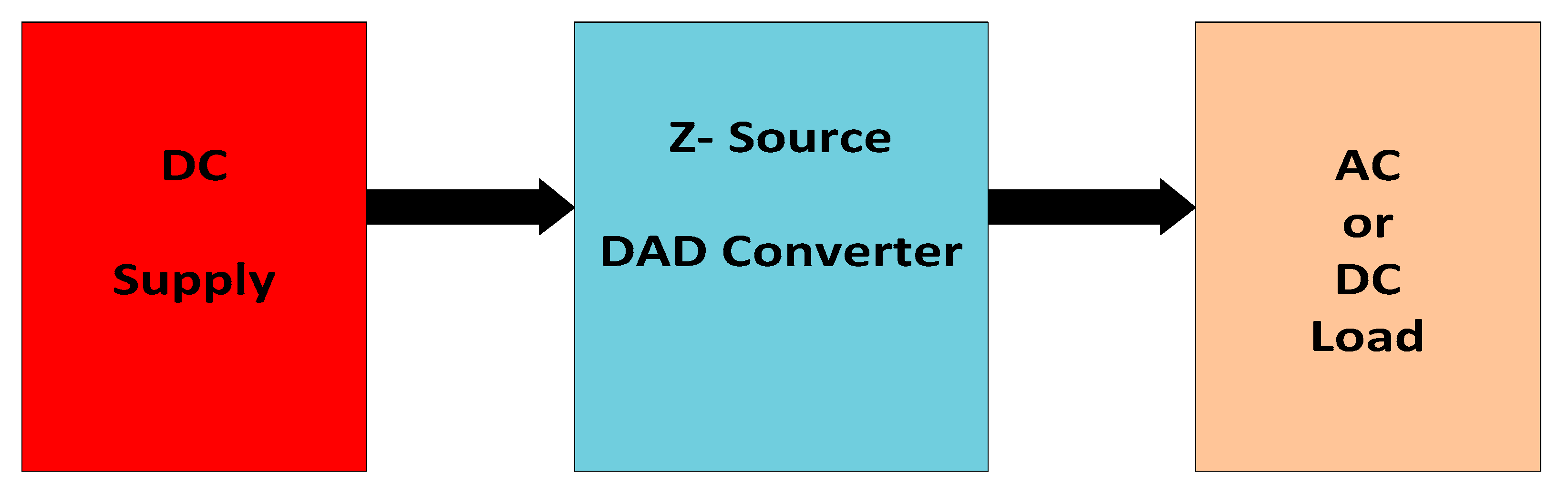
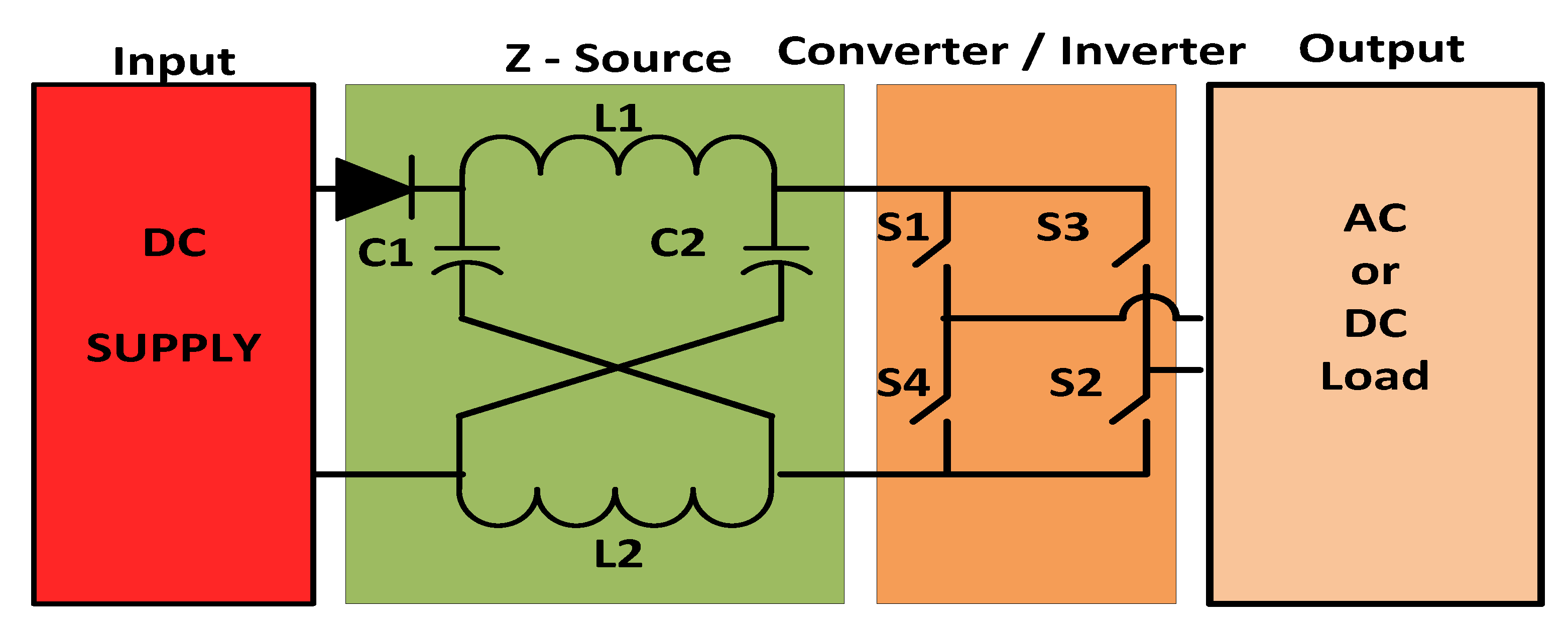
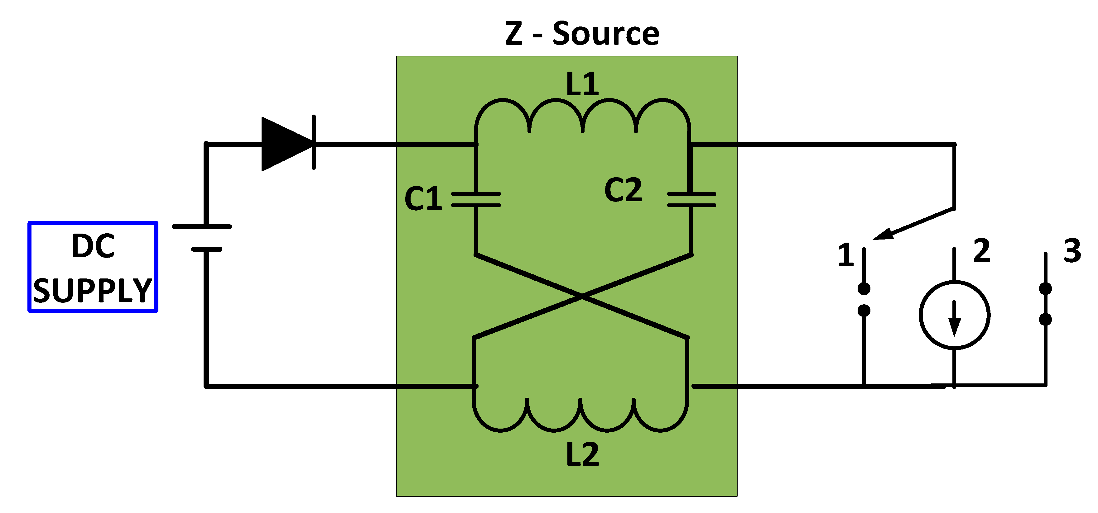
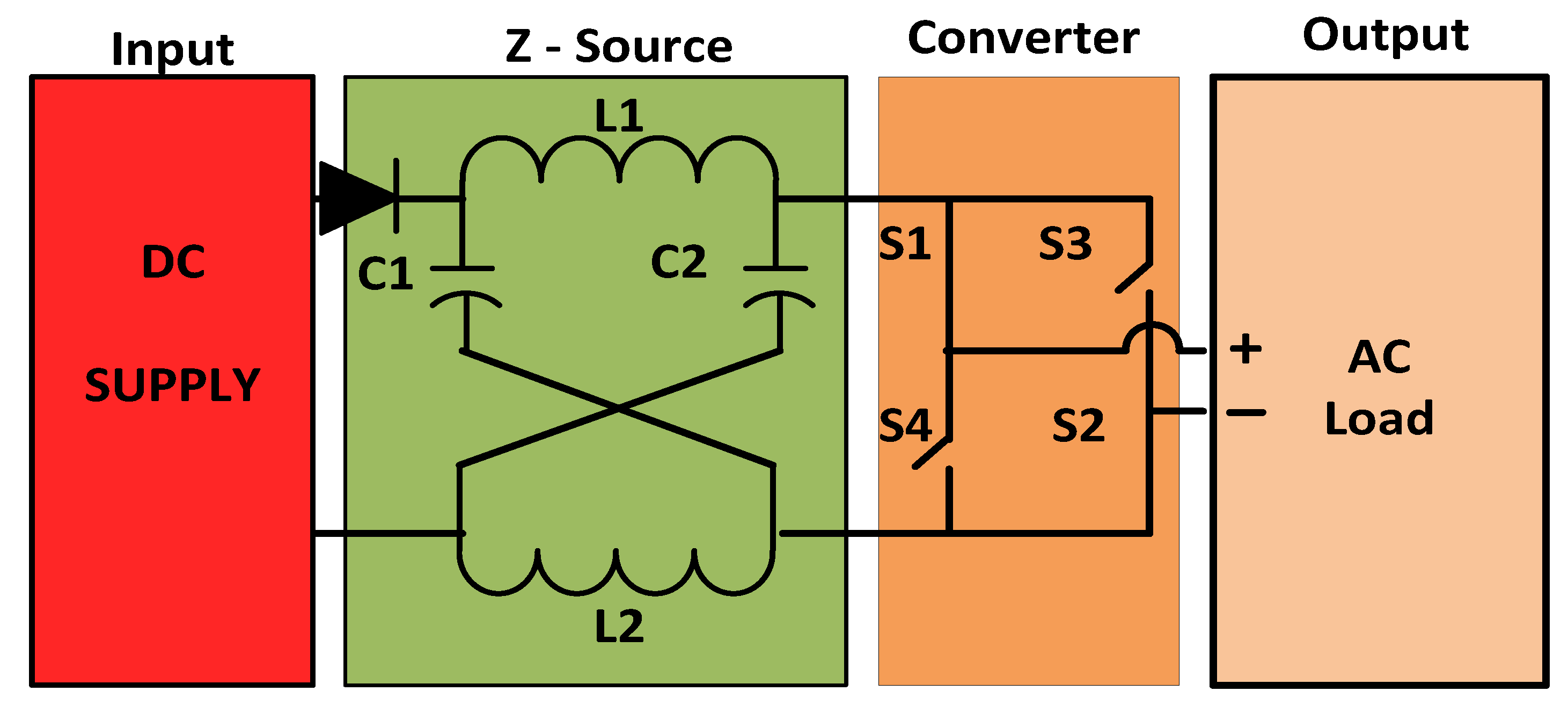
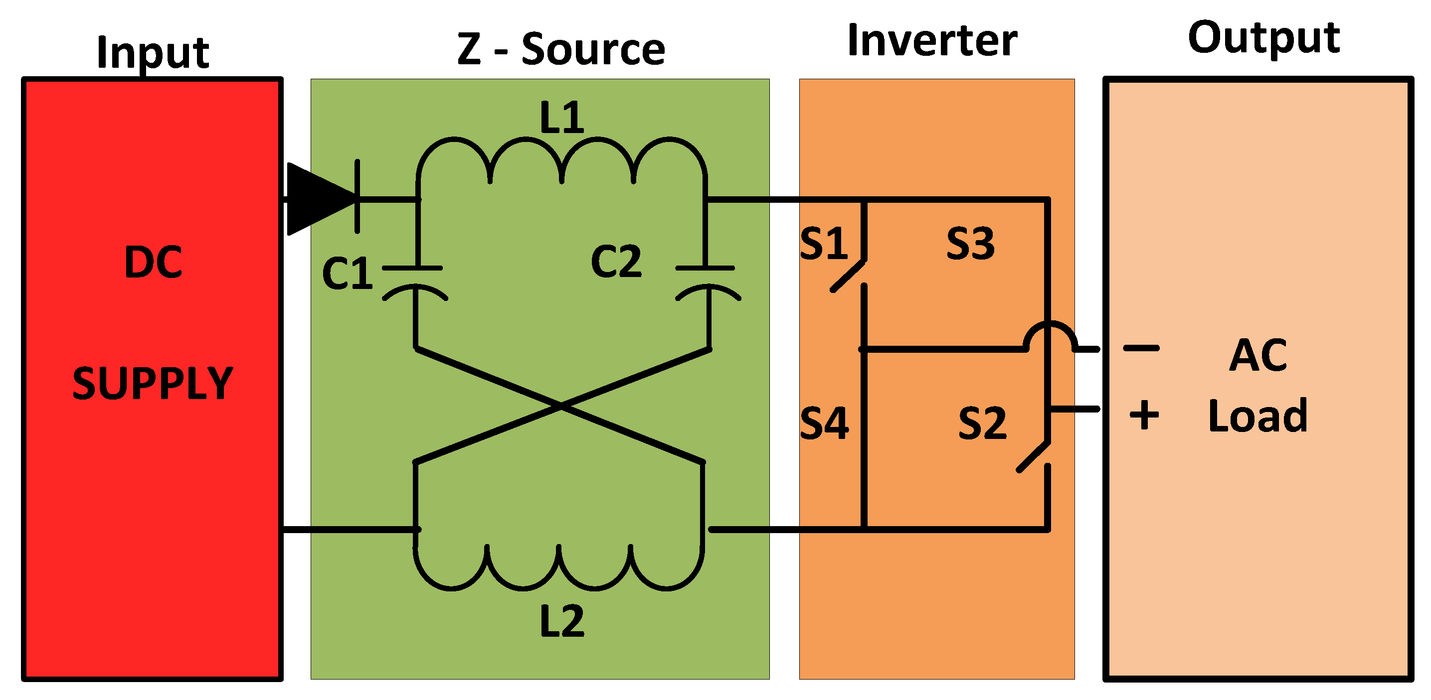
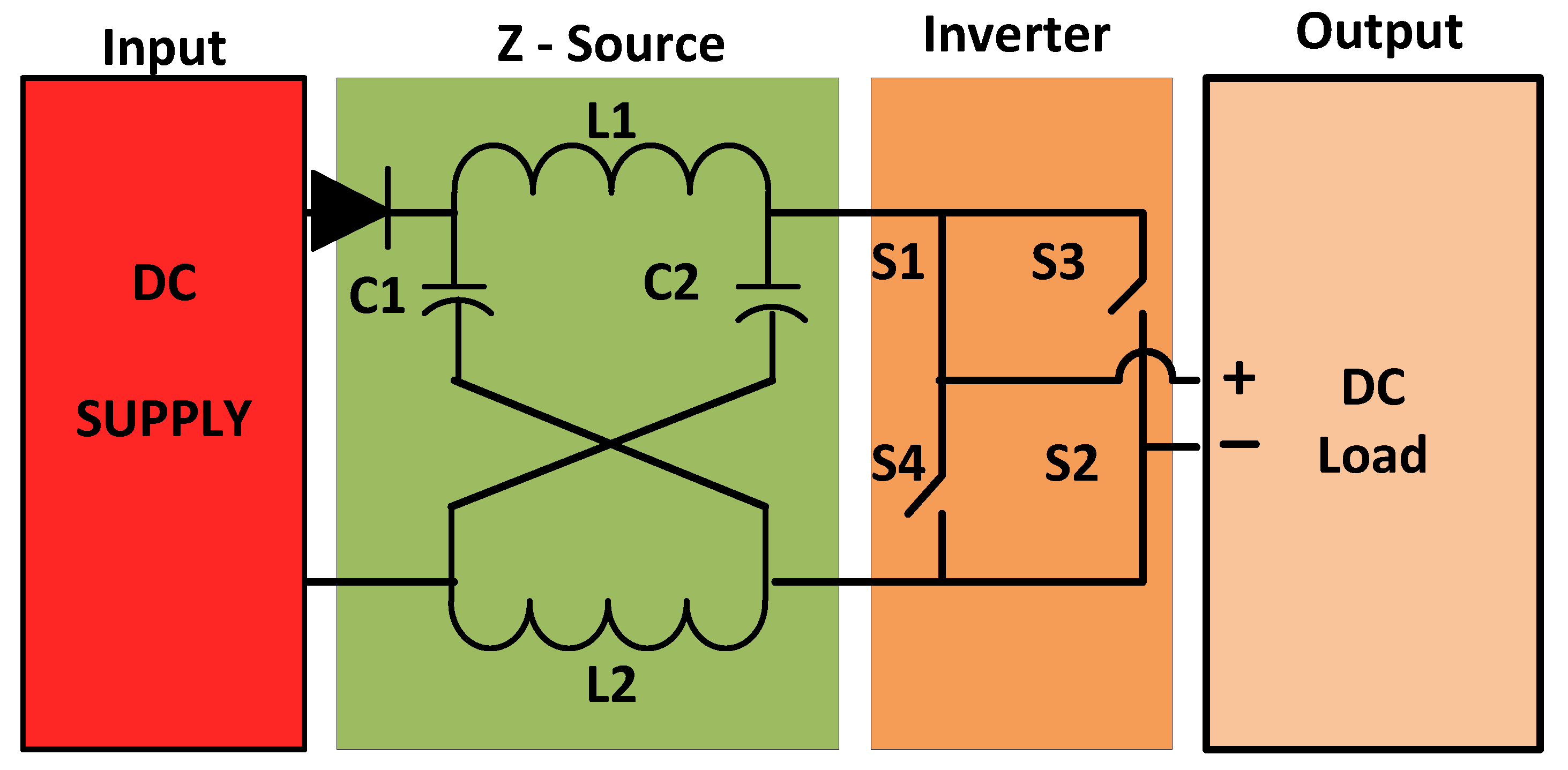
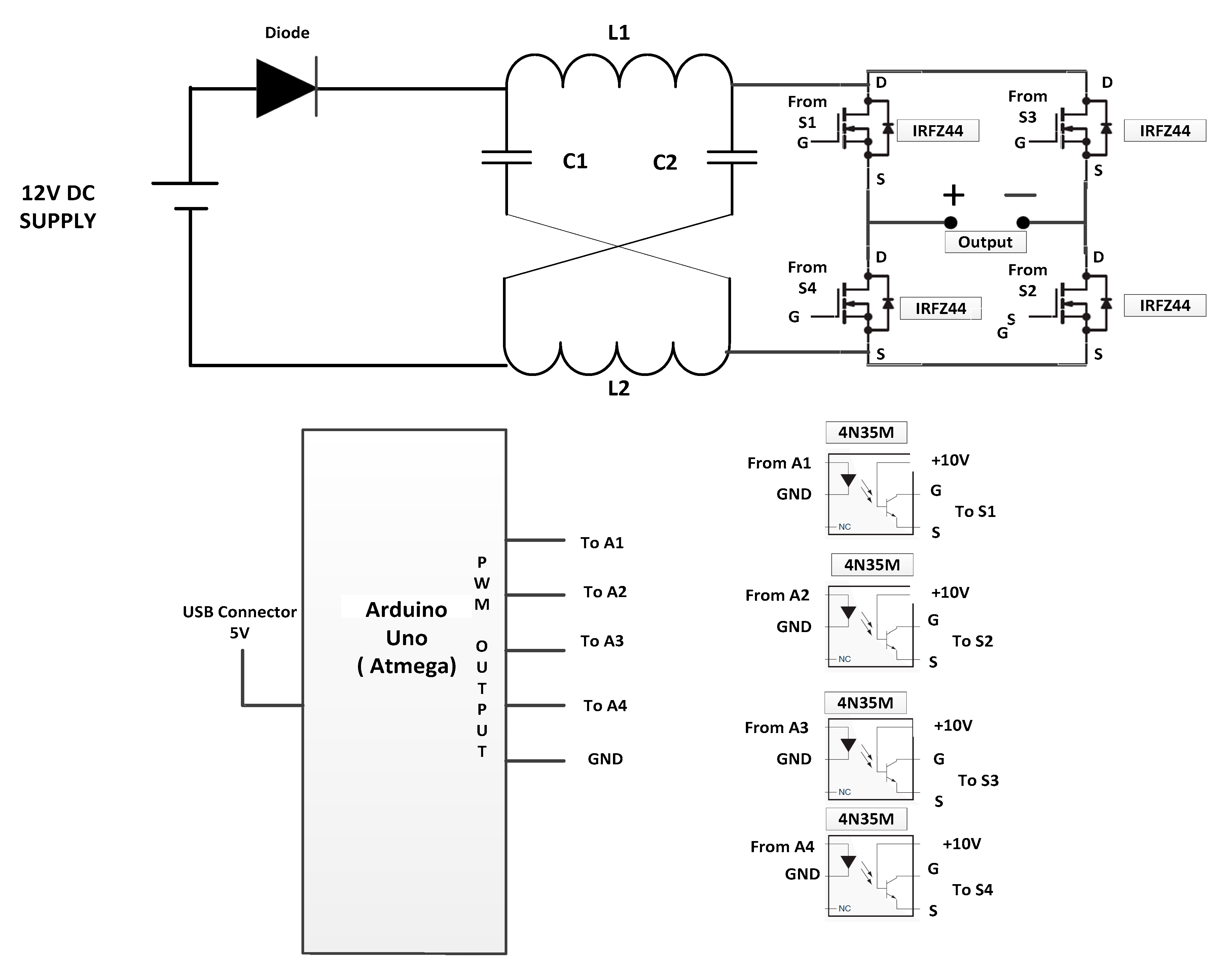
2. Z-Source DAD Converter
The Z-Source DAD converter consists of an impedance source network connected between the input DC supply and the converter circuit, as shown in Figure 1. The Z-Source arrangement creates the buck and boost ability of the inverter and the converter circuit [1,13].
Figure 1.
Z-Source direct current (DC)-to-alternating current (AC)/DC (DAD) converter system.
This Z-Source network employs split inductors and split capacitors arranged in an X shape. This Z-Source network is a two-port network with split inductors L1 and L2 and split capacitors C1 and C2 [1,13]. These components are arranged in an X shape between the system input supply and the converter circuit, as shown in Figure 2. This arrangement, along with the converter circuit, can directly convert the input DC to output AC or DC of higher or lower magnitude by controlling the duty cycle or MI along with the shoot-through duration. The circuit arrangement of the Z-Source DAD converter is shown in Figure 2.
Figure 2.
Simplified circuit arrangement of Z-Source DAD converter. (L1, L2 split inductors, C1, C2 split capacitors, S1–S4 switches).
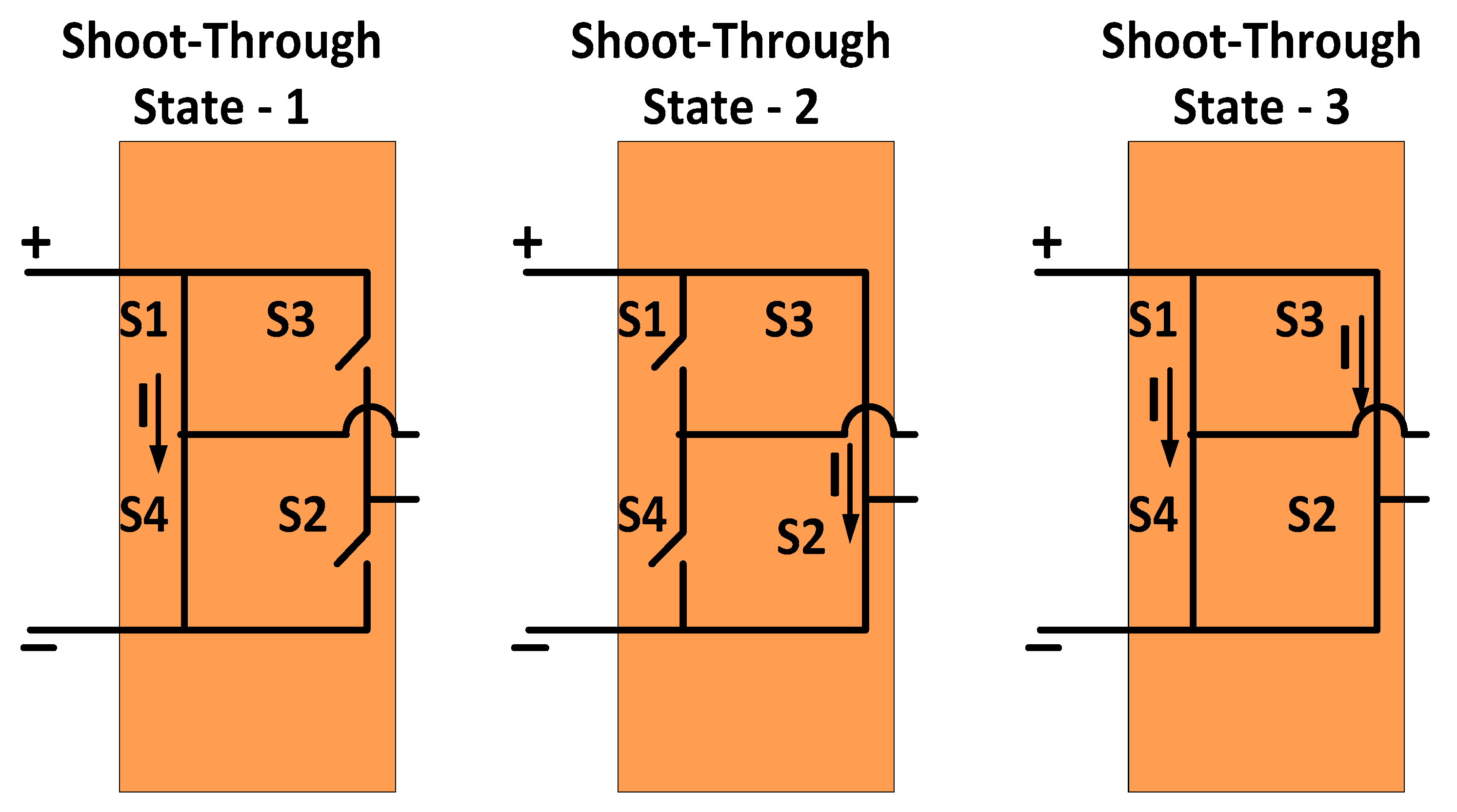
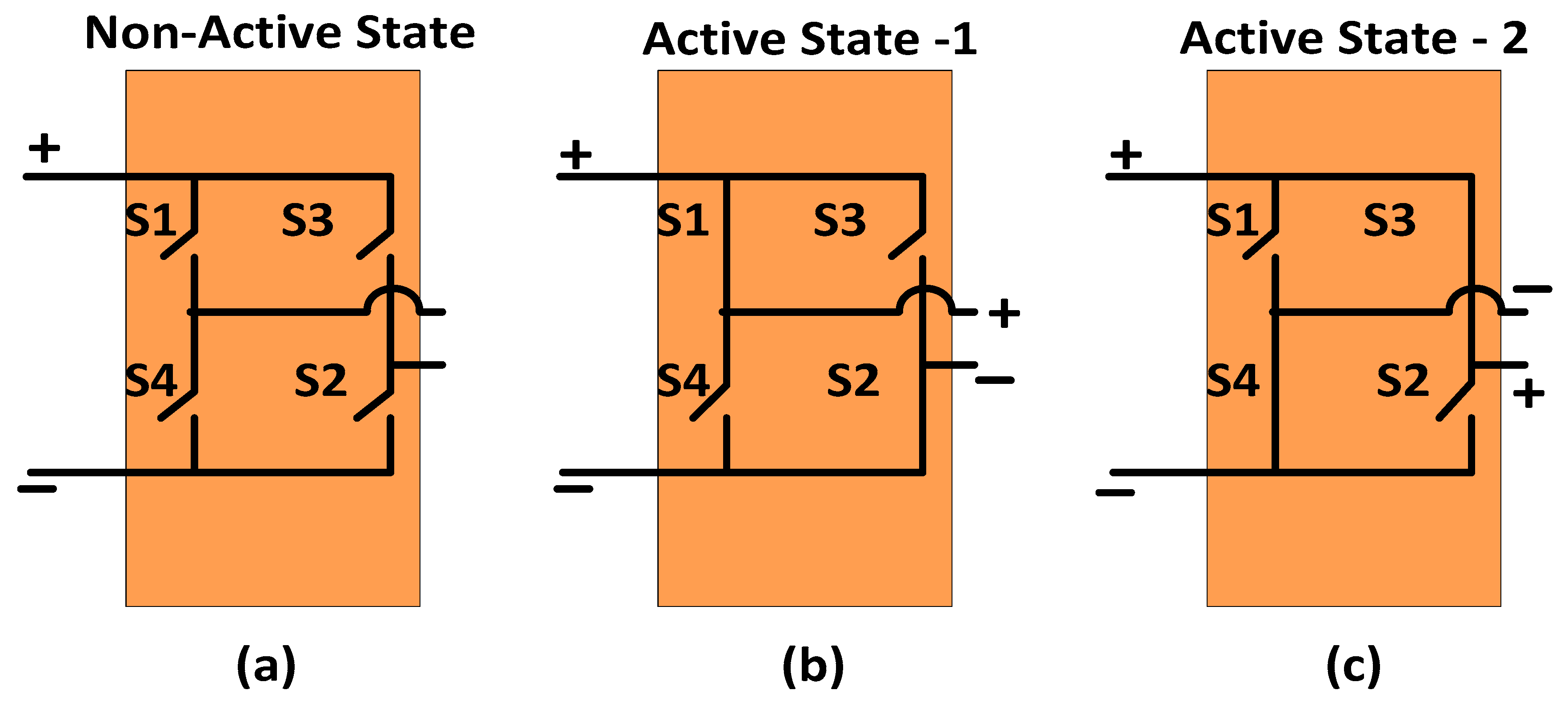
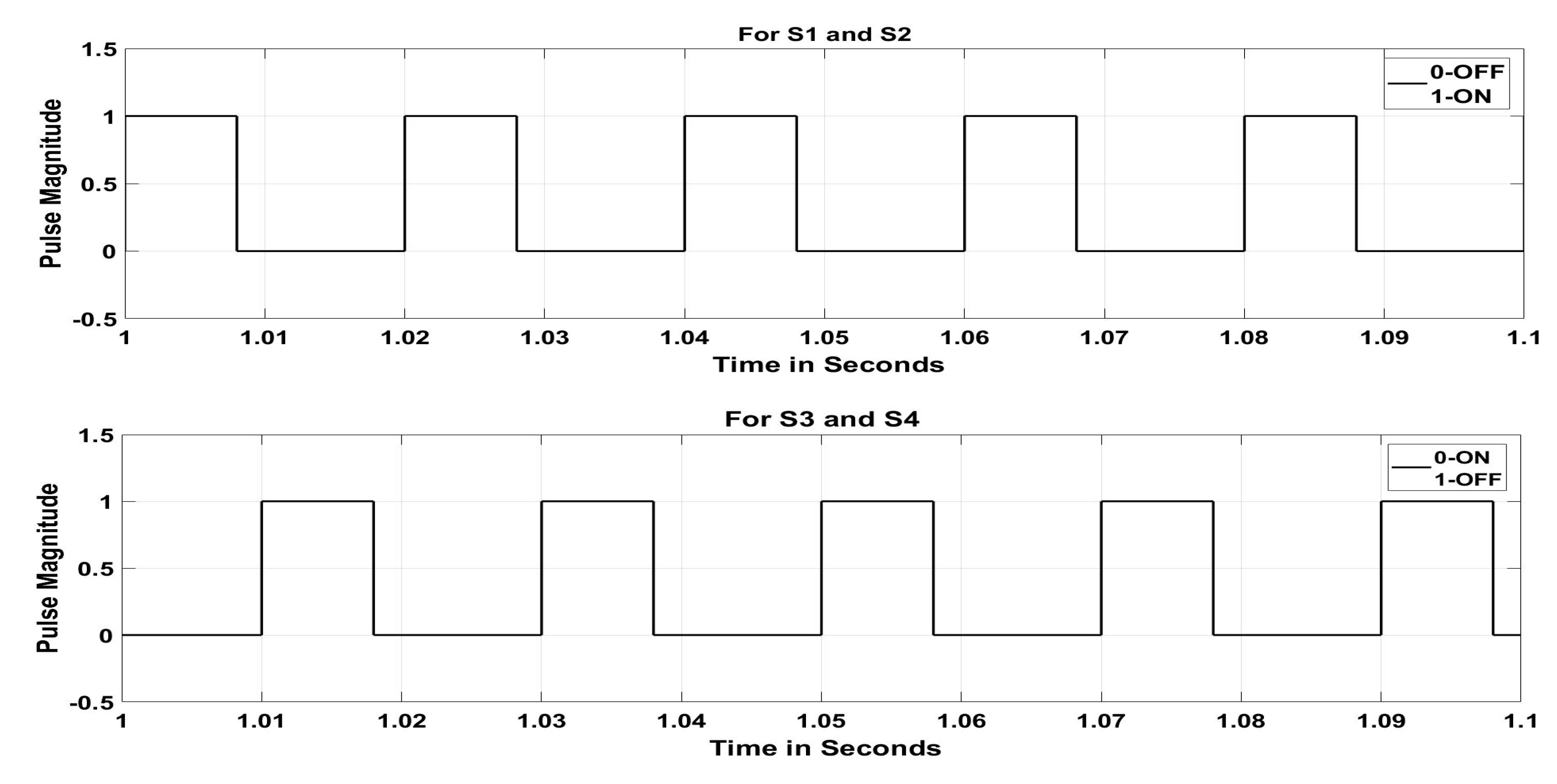
3. Operating Principle
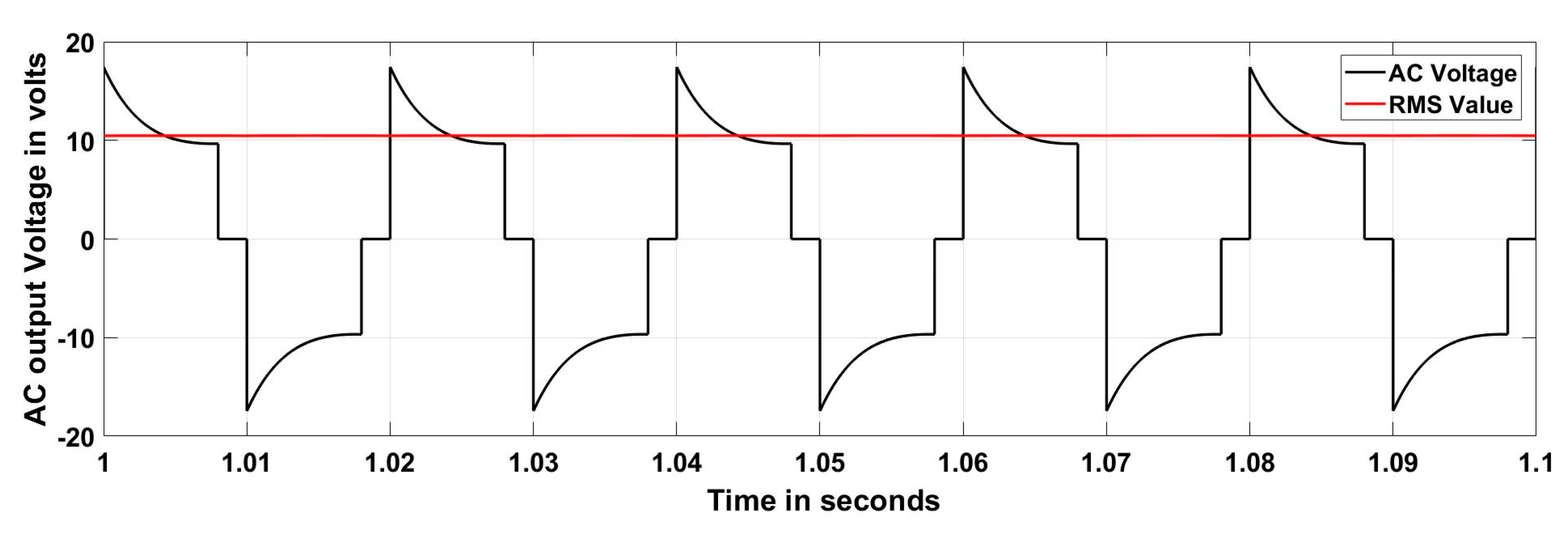
As shown in Figure 3, the Z-Source DAD converter can operate in three states: (1: open state, 2: active state, and 3: shoot-through (ST) state). In the active state, the energy transfer occurs between the input and the load, whereas in the open state and zero state, no energy transfer takes place between the input and the load. In the ST state, the switches S1–S4 or S2–S3 are switched on, which leads to the short circuit of the Z-source network. During this time, the diode is reverse-biased, and energy is transferred from C1 to L1 and C2 to L2.
Figure 3.
Operating states of the Z-Source DAD converter. (1: open state, 2: active state, 3: shoot-through (ST) state).
The ST state is initiated by closing the S1–S4 or S3–S2 of the converter. The ST state can be achieved in three ways, as shown in Figure 4. ST state-1 can be achieved by closing the first and fourth switches, ST state-2 by closing the second and third switches, and ST state-3 by closing all the switches. Any one of the ST states can be used to obtain the shoot-through. The ST time duration decides the magnitude of the boost in the output voltage. Therefore, any one of the ST states is implemented in the converter or inverter circuit to produce a higher-value load voltage. The ST state is not required for buck mode operation where the output AC or DC voltage is less than the input DC voltage.
Figure 4.
ST zero states.
In the non-active state, all the switches are open. Therefore, no energy is drawn from the supply, and no energy is supplied to the load. During active state-1, S1 and S2 are turned on, then the load receives positive voltage; in active state-2, S3 and S4 are turned on, then the load receives negative voltage. Figure 5 shows the non-active and active states. The non-active state and active state durations determine the output voltage in buck mode, whereas the ST duration along with the active and non-active durations determines the magnitude of the output voltage in boost mode operation. On the basis of the load requirement, the DAD converter output is switched over between AC or DC with buck or boost in the load voltage for the given DC input supply.
Figure 5.
Non-active and active states: (a) non-active state, (b) active state-1, and (c) active state-2.
3.1. Inverter Mode
In this mode input, DC voltage is converted into AC voltage. For this purpose, switches 1 and 2 are turned on for the first half cycle (positive) duration, as shown in Figure 6, and switches 3 and 4 are turned on for the next (negative) half cycle, as shown in Figure 7. This mode produces the buck mode of operation, and the output voltage is:
where M is the Modulation Index, and Vdc is the DC link voltage.
Figure 6.
Z-Source DAD converter, inverter mode (positive half cycle).
Figure 7.
Z-Source DAD converter, inverter mode (negative half cycle).
For boost mode, an ST state is used to achieve the boost in the voltage. The ST state is the zero state of the inverter. During this time, no energy transfer occurs between the input and output, therefore this state is also called a zero state. With the help of the ST state, the boost in magnitude of the output voltage is controlled [14,15,16,17]. In this mode, the output AC voltage is:
where
where T1 is the active state duration, T0 is the ST state duration, and T is the total duration.
3.2. Converter Mode
The converter mode of operation operates as a DC–DC boost or buck converter. In buck mode, by keeping switches 3 and 4 open and controlling switches 1 and 2, the output voltage can be controlled, as shown in Figure 8. In buck mode, the output DC voltage is:
By adjusting the duty cycle (D), the output DC is controlled. Here, the magnitude of output is less than that of the DC input.
Figure 8.
Z-Source DAD converter,–DC–DC converter mode.
For boost mode, any one of the ST states is introduced before the active state. In this mode, the output voltage is:
By controlling the boost factor (B), the load DC voltage magnitude is varied. Here, the load voltage is always higher than the magnitude of the DC link voltage. By varying the ST duration, the boost factor can be controlled.
4. Design of Z-Source
The split capacitor (C1, C2) and the split inductor (L1, L2) are selected on the basis of the buck–boost requirement of the system. Normally, the capacitor rating is nearer to the rating of the input capacitor of the VSI [13]. The capacitor rating can be found by using Equations (6)–(8). The inductor rating is nearer to the input side inductor rating of the CSI [13]. The inductor value can be found using Equation (9). The capacitor and inductor can also be designed by taking the buck–boost converter design or the Z-Source design of the simple Z-Source inverter [1,13]. In general, the capacitor value is obtained using the value of the current through the inductor (Il) and the change in the capacitor voltage ():
The voltage stress across the capacitor is
where
The value of the inductor can be determined using the voltage across the capacitor () and the change in the inductor current ():
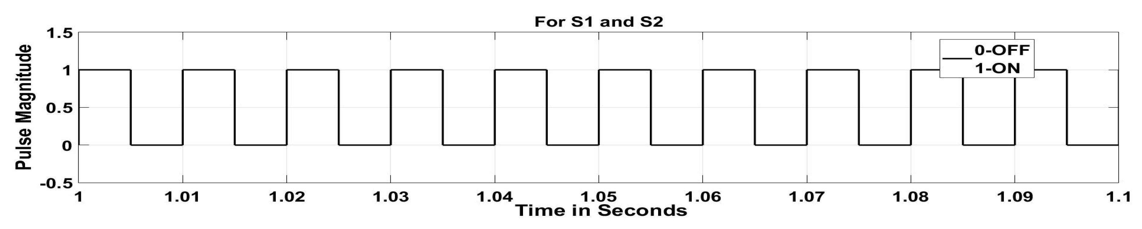
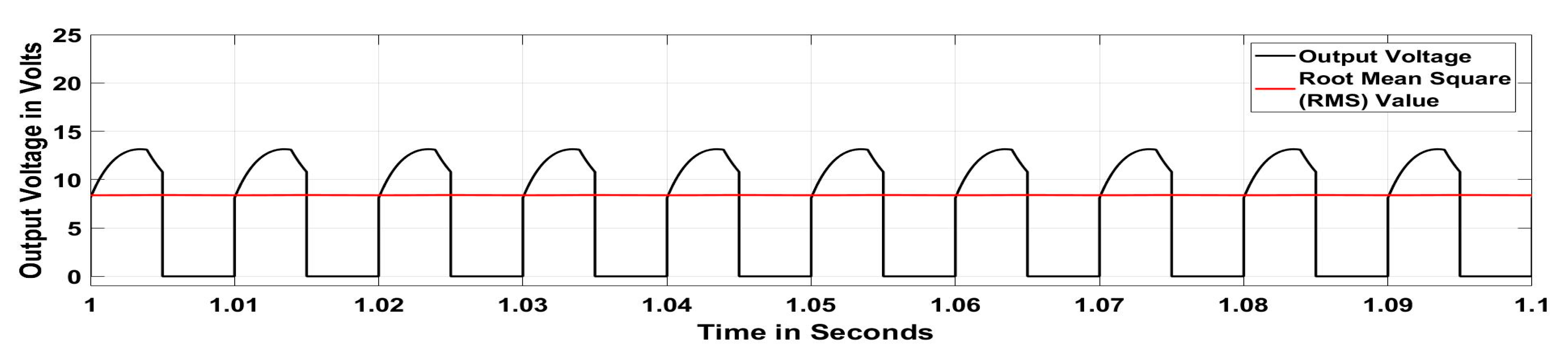
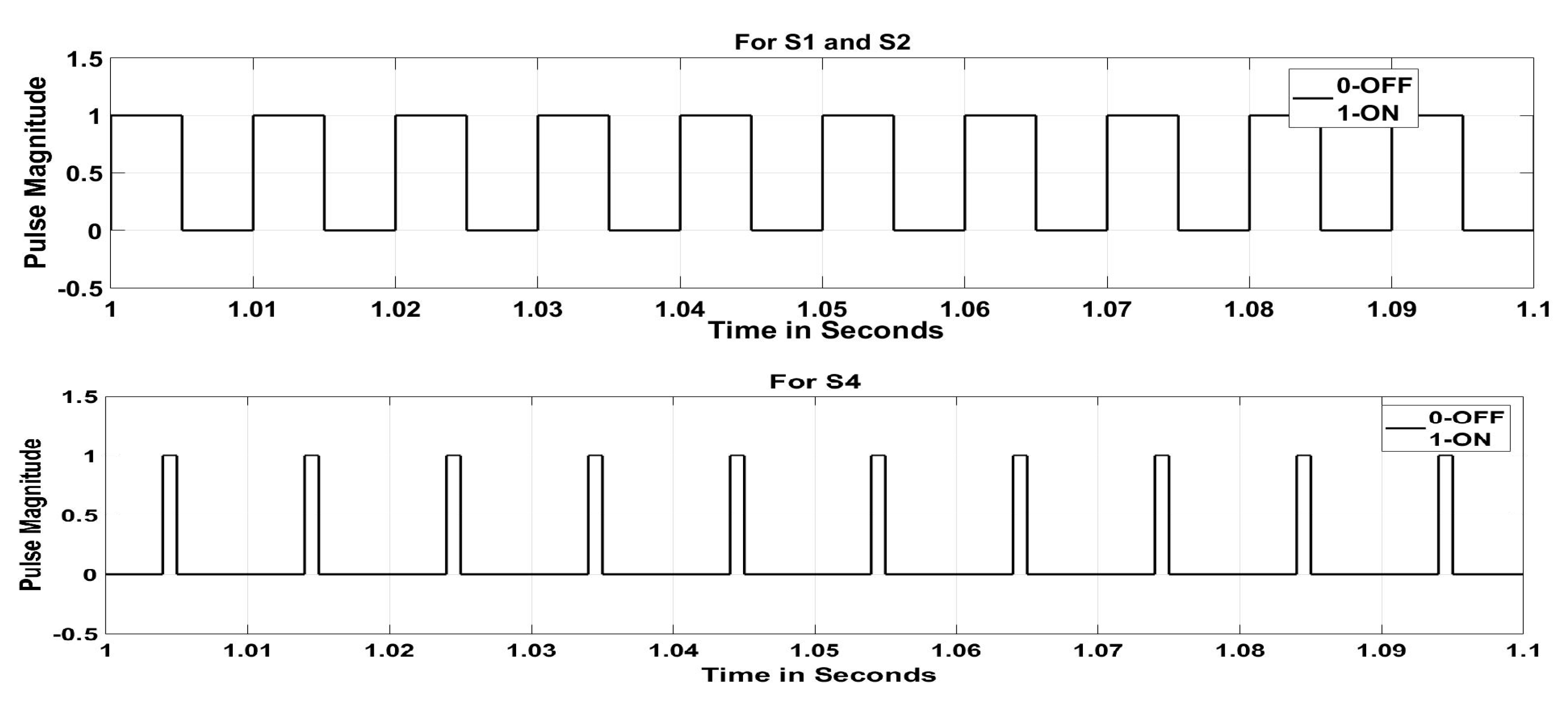
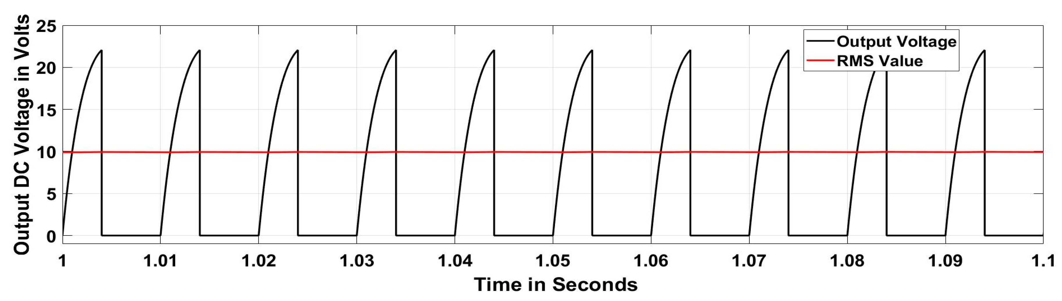
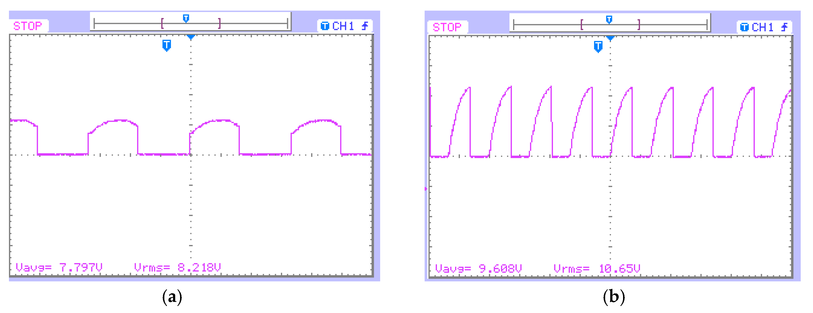
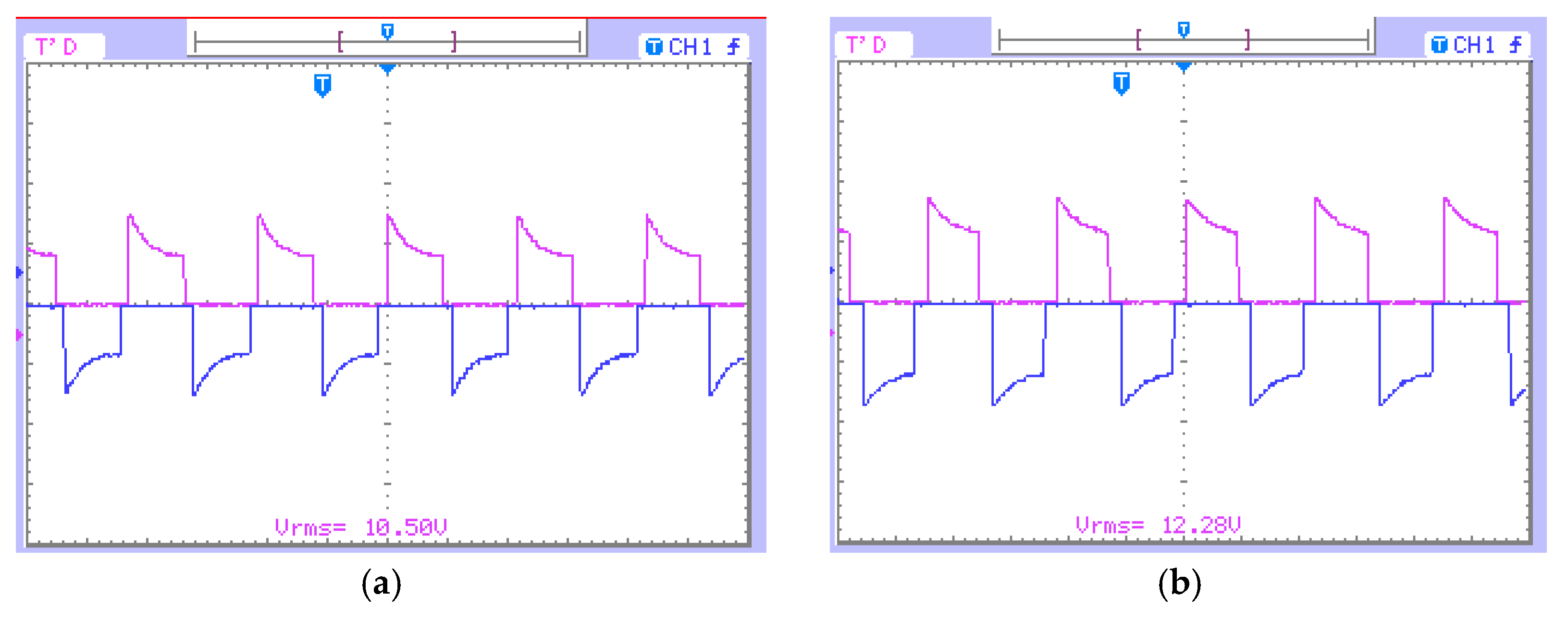
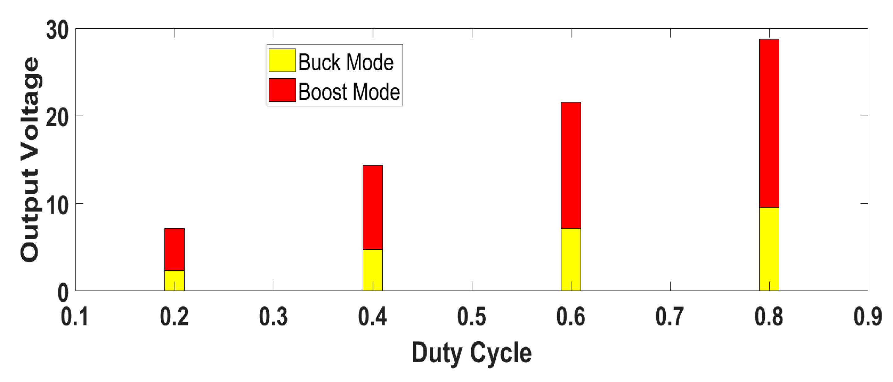
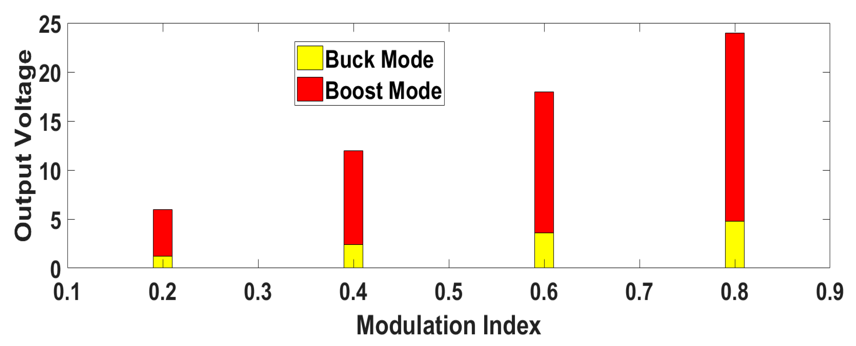
5. Simulation and Experimental Results
A MATLAB-Simulink (The MathWorks, Massachusetts, USA) simulation was conducted to analyze the performance of the proposed Z-Source DAD converter with the Z-source element values of C1 = C2 = 100 µF and L1 = L2 = 250 mH, 12 Volt DC input, and a load resistance of 50 Ω. The same circuit parameters were used to construct the hardware circuit; the control pulses to the switches were generated using an ATmega (Microchip, AZ, USA)-microcontroller-based circuit board, as shown in Figure 9. The hardware setup consisted of four IRFZ44 MOSFETS used as a switch (S1–S4) and four 4N35M optocouplers used to connect the microcontroller circuit with the converter switches. The optocouplers provided electrical isolation between the low-power microcontroller circuits and the high-power converter circuit. The MATLAB-Simulink simulation and the hardware circuit were tested for both the inverter and the converter circuits operation. The buck and boost modes were applied to both the inverter and the converter circuits. The outcome of the simulation and hardware results are shown below.
Figure 9.
Hardware setup.
Figure 10 and Figure 11 show the control pulse and output DC voltage for the DAD converter for DC-to-DC buck mode operation with a duty cycle of 0.5 and without ST timing. Figure 12 and Figure 13 show the control pulse and output DC voltage for the DAD converter in DC-to-DC boost mode operation with duty cycle of 0.5 and ST timing of 0.001 s. By introducing the ST timing, the buck converter switched over to boost mode, demonstrating the ability of the DAD converter to increase or decrease the voltage magnitude of the given input DC voltage (Figure 11 and Figure 13). The experimental wave forms are shown in Figure 14.
Figure 10.
Simulink simulation of control pulses for DC–DC buck mode.
Figure 11.
Simulated output of DC–DC buck mode load voltage.
Figure 12.
Simulink simulation of control pulse for DC–DC boost mode.
Figure 13.
Simulated output of DC–DC boost mode load voltage.
Figure 14.
Experimental output voltage waveforms for an input DC voltage of 12V: (a) Output voltage of DC–DC buck mode with D = 0.5 (b) Output voltage of DC–DC boost mode with D = 0.5 and ST = 0.1. (Voltage: 10 V/div, Time: 10 ms/div).
Figure 15 and Figure 16 show the control pulse and output AC voltage of the DAD converter in buck mode operation with a modulation index of 0.8 and without ST timing. The Fast Fourier Transform (FFT) analysis is depicted in Figure 17 to understand the harmonic components. By introducing the ST timing of 0.004 s, the same buck inverter acted as a boost inverter. Figure 18 and Figure 19 show the control pulse and output AC voltage of the DAD converter in boost mode operation with a modulation index of 0.8 and ST timing of 0.004 s. Figure 20 provides the harmonic analysis of the output AC voltage. This buck–boost feature in both converter and inverter modes increases the suitability of the DAD converter for photovoltaic systems by eliminating the number of power converting stages in distributed generating systems [18,19,20,21].
Figure 15.
Control pulse for inverter mode in buck mode.
Figure 16.
Simulated output of output voltage for inverter mode in buck mode.
Figure 17.
Simulated Fast Fourier Transform (FFT) analysis of buck inverter output with Total Harmonic Distortion (THD).
Figure 18.
Simulink simulation of control pulse for inverter boost mode.
Figure 19.
Simulated output of output voltage for inverter in boost mode.
Figure 20.
Simulated FFT analysis of boost mode inverter output with THD.
Experimental wave forms for DC–AC inverters are shown in Figure 21. The above results indicate that the Z-Source DAD converter is capable of converting the given DC input voltage into AC or DC output voltages with buck or boost in the magnitude. The boost in the output voltage can be varied by adjusting the duty cycle or modulation index along with the shoot-through timing of the converter. The ST timing is not required for buck mode operation. Figure 22 and Figure 23 compare the experimental output voltages between the buck and boost modes of both converter and inverter operation of the Z-Source DAD converter.
Figure 21.
Experimental output voltage waveforms for an input DC voltage of 12 V: (a) buck mode inverter output with modulation index (MI) = 0.8; (b) boost mode inverter output with MI = 0.8 and ST = 0.1 (Voltage: 10 V/div, Time: 10 ms/div).
Figure 22.
Experimental DC–DC converter voltage comparison of buck mode and boost mode with a boost factor of 2.
Figure 23.
Experimental DC–AC inverter output voltage comparisons of buck mode and boost mode with a boost factor of 4.
6. Conclusions
This Z-Source DAD converter converts the given DC input into either AC or DC with buck or boost in the voltage magnitude. However, the existing Z-Source converters produce only one type of output (either AC or DC) with buck or boost in the voltage magnitude. The buck–boost feature of the Z-Source DAD converter reduces the two-stage power converter circuit required by renewable energy applications like solar PV systems. This converter can be widely used in PV energy systems. During the daytime, the Z-Source DAD converter operates as a DC–DC converter and stores PV power in a battery or supplies power to the DC load. During the night-time, the battery power is converted to AC by the same converter to operate residential appliances. The Z-Source DAD converter can be used for both AC and DC loads. Thus, the Z-Source DAD converter operates easily when compared with normal DC–DC or DC–AC conversion and reduces the number of components, thereby decreasing the size of the power converter circuit. The overall cost of the Z-Source DAD converter is less, and the size is smaller than those of the normal two-stage power converter circuit.
Author Contributions
R.S. and D.E. developed the proposed research work, implemented MATLAB-Simulink simulation, and also developed the microcontroller-based converter hardware for the performance validation of the proposed converter circuit. Both authors were involved in framing the current format of the full research paper work.
Funding
This research received no external funding.
Conflicts of Interest
The authors declare no conflicts of interest.
References
- Peng, F.Z. Z-source inverter. IEEE Trans. Ind. Appl. 2003, 39, 504–510. [Google Scholar] [CrossRef]
- Yu, Y.; Zhang, Q.; Liang, B.; Liu, X.; Cui, S. Analysis of Single-Phase Z-Source Inverter for Battery Discharging in Vehicle to Grid Applications. Energies 2011, 4, 2224–2235. [Google Scholar] [CrossRef]
- Huang, S.; Zhang, Y.; Shuai, Z. Capacitor Voltage Ripple Suppression for Z-Source Wind Energy Conversion System. Energies 2016, 9, 56. [Google Scholar] [CrossRef]
- Zhang, Y.; Shi, J.; Fu, C.; Zhang, W.; Wang, P.; Li, J.; Sumner, M. An Enhanced Hybrid Switching Frequency Modulation Strategy for Fuel Cell Vehicle Three-Level DC-DC Converters with Quasi-Z-Source. Energies 2018, 11, 1026. [Google Scholar] [CrossRef]
- Ellabban, O.; Van Mierlo, J.; Lataire, P. Control of A High-Performance Z-Source Inverter for Fuel Cell/ Supercapacitor Hybrid Electric Vehicles. Electr. Veh. J. 2010, 4, 444–451. [Google Scholar] [CrossRef]
- Sreeprathab, N.R.; Felix Joseph, X. A survey on Z-source inverter. In Proceedings of the 2014 International Conference on Control, Instrumentation, Communication and Computational Technologies (ICCICCT), Kanyakumari, India, 10–11 July 2014. [Google Scholar]
- Ellabban, O.; Abu-Rub, H. Z-source inverter: Topology improvements review. IEEE Ind. Electron. Mag. 2016, 10, 6–24. [Google Scholar] [CrossRef]
- Wang, B.; Tang, W. A New CUK-Based Z-Source Inverter. Electronics 2018, 7, 313. [Google Scholar] [CrossRef]
- Li, Y.; Jiang, S.; Cintron-Rivera, J.G.; Peng, F.Z. Modeling and control of quasi-Z-source inverter for distributed generation applications. IEEE Trans. Ind. Electron. 2013, 60, 1532–1541. [Google Scholar] [CrossRef]
- Kalaiarasi, N.; Subranshu, S.D.; Snajeevikumar, P.; Paramasivam, S.; Pandav, K.M. Maximum Power Point Implementation by Dspace Controller Integrated Through Z-Source Inverter Using Particle Swarm Optimization Technique for Photovoltaic Applications. Appl. Sci. 2018, 8, 145. [Google Scholar]
- Ahmed, T.; Soon, T.K.; Mekhilef, S. A Single Phase Doubly Grounded Semi-Z-Source Inverter for Photovoltaic (PV) Systems with Maximum Power Point Tracking (MPPT). Energies 2014, 7, 3618–3641. [Google Scholar] [CrossRef]
- Subhani, N.; Kannan, R.; Mahmud, M.A.; Romlie, M.F. Performance Analysis of a Modernized Z-Source Inverter for Robust Boost Control in Photovoltaic Power Conditioning Systems. Electronics 2019, 8, 139. [Google Scholar] [CrossRef]
- Rajakaruna, S.; Jayawickrama, L. Steady-state analysis and designing impedance network of Z-source inverters. IEEE Trans. Ind. Electron. 2010, 57, 2483–2491. [Google Scholar] [CrossRef]
- Shen, M.; Wang, J.; Joseph, A.; Peng, F.Z.; Tolbert, L.M.; Adams, D.J. Maximum constant boost control of the Z-source inverter. In Proceedings of the 2004 IEEE Industry Applications Conference, Seattle, WA, USA, 3–7 October 2004. [Google Scholar]
- Huang, S.; Zhang, Y.; Hu, S. Stator Current Harmonic Reduction in a Novel Half Quasi-Z-Source Wind Power Generation System. Energies 2016, 9, 770. [Google Scholar] [CrossRef]
- Sebtahmadi, S.S.; Azad, H.B.; Islam, D.; Seyedmahmoudian, M.; Horan, B.; Mekhilef, S.; Seyedmahmoudian, M. A Current Control Approach for an Abnormal Grid Supplied Ultra Sparse Z-Source Matrix Converter with a Particle Swarm Optimization Proportional-Integral Induction Motor Drive Controller. Energies 2016, 9, 899. [Google Scholar] [CrossRef]
- Nguyen, M.-K.; Choi, Y.-O. Maximum Boost Control Method for Single-Phase Quasi-Switched-Boost and Quasi-Z-Source Inverters. Energies 2017, 10, 553. [Google Scholar] [CrossRef]
- Sajadian, S.; Ahmadi, R. ZSI for PV systems with LVRT capability. IET Renew. Gener. 2018, 12, 1286–1294. [Google Scholar] [CrossRef]
- Singh, S.A.; Carli, G.; Azeez, N.A.; Williamson, S.S. Modeling, Design, Control, and Implementation of a Modified Z-Source Integrated PV/Grid/EV DC Charger/Inverter. IEEE Trans. Ind. Electron. 2018, 65, 5213–5220. [Google Scholar] [CrossRef]
- Hanif, M.; Basu, M.; Gaughan, K. Understanding the operation of a Z-source inverter for photovoltaic application with a design example. IET Electron. 2011, 4, 278–287. [Google Scholar] [CrossRef]
- Liu, Y.; Abu-Rub, H.; Ge, B. Z-Source\/Quasi-Z-Source Inverters: Derived Networks, Modulations, Controls, and Emerging Applications to Photovoltaic Conversion. IEEE Ind. Electron. Mag. 2014, 8, 32–44. [Google Scholar] [CrossRef]
© 2019 by the authors. Licensee MDPI, Basel, Switzerland. This article is an open access article distributed under the terms and conditions of the Creative Commons Attribution (CC BY) license (http://creativecommons.org/licenses/by/4.0/).