Article

A Highly Linear Low-Noise Transimpedance Amplifier for Indoor Fiber-Wireless Remote Antenna Units

by
Guillermo Royo
*,
Antonio D. Martinez-Perez
,
Carlos Sanchez-Azqueta
,
Concepcion Aldea
and
Santiago Celma
Group of Electronic Design—Aragón Institute of Engineering Research, Universidad de Zaragoza, 50009 Zaragoza, Spain
*
Author to whom correspondence should be addressed.
Electronics 2019, 8(4), 437; https://doi.org/10.3390/electronics8040437
Submission received: 15 March 2019 / Revised: 9 April 2019 / Accepted: 12 April 2019 / Published: 16 April 2019
(This article belongs to the Section Microelectronics)

Abstract

:
This article presents an optimized design of a low-noise transimpedance amplifier (TIA) with high linearity for use in the downlink receiver of a remote antenna unit (RAU). The aim of this design is to be used in a cost-effective indoor distributed antenna system (DAS) for WLAN transmission using a mixed fiber-wireless system. The circuit topology consists of a fully differential shunt–shunt feedback TIA with digitally programmable transimpedance. An open-loop gain compensation technique is used to maintain stability and constant bandwidth (BW). The TIA has been fabricated in 65 nm CMOS technology with a 1.2 V voltage supply. The total power consumption of the TIA is 6 mW. A complete electrical and optical characterization with a 1550 nm PIN photodiode has been performed to demonstrate the reliable 54 Mb/s 802.11a WLAN transmission achieved with an error vector magnitude (EVM) lower than 3% for a 20 dB optical input range.

1. Introduction

The increase in demand for mobile devices has driven the development of wireless systems over the last few years. The main requirements of these new communication systems are good accessibility and robustness, achieving high data capacity. Actual short-range indoor wireless networks must enhance their coverage and show a higher immunity to interferences with neighboring networks with a signal distribution that is better confined in the volume of interest.
In this context, the integration of fiber-wireless networks has emerged as a promising solution to support the rate of growth of data traffic demand for wireless applications, either indoor or outdoor, combining the best of these technologies: the mobility of wireless technologies and the low attenuation and large bandwidth (BW) of optical fibers.
The interest in mixed fiber-wireless systems has grown in recent years, especially for short-range indoor applications, which can benefit from radio-over-fiber (RoF) distributions, as is the case with distributed antenna systems (DASs) [1,2]. These systems are flexible and there is a good compromise between data capacity, accessibility, and the overall cost of installation and maintenance, allowing for a good convergence of optical fiber capacity and wireless access flexibility [
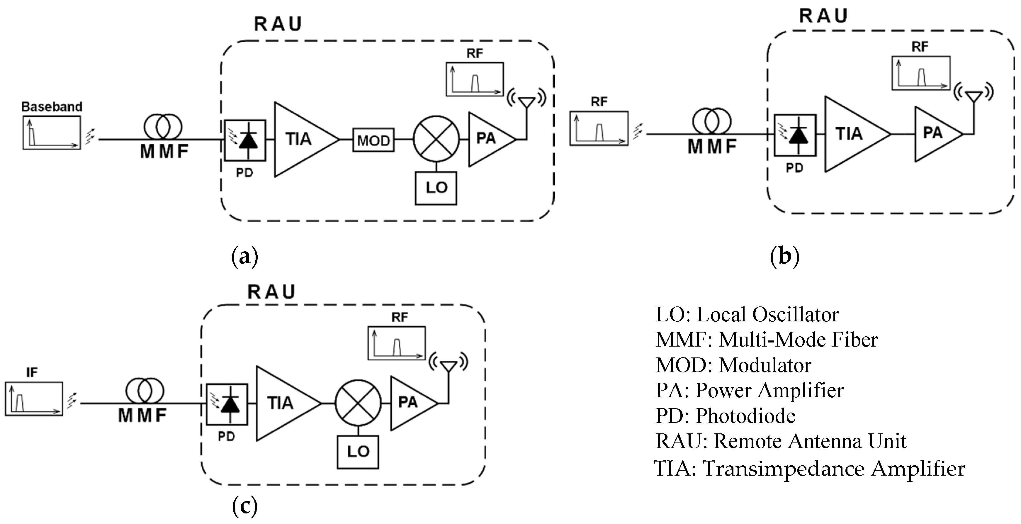
3]. The system operation consists of distributing the signal through multi-mode fiber (MMF) from a base station (BS) to distributed remote antenna units (RAUs), which provide an optical-wireless interface (see Figure 1). To decrease the effects of fiber chromatic dispersion, the wireless signals can be down-converted before the optical transmission, employing an intermediate frequency (IF) communication scheme [4].
The key of a DAS is to employ cost-effective components in the three main elements of the communication system. This is achieved with the use of MMF, which presents immunity to electromagnetic interferences and offers a large BW, and therefore a very high data capacity, along with cost-effective photonic devices, such as vertical-cavity surface-emitting lasers (VCSEL), and a low-cost, low-power design of the RAUs, with low-cost transceivers and a design of moderate complexity. Figure 2 shows three different downlink RAU configurations, depending on how the data transmission is performed: (a) baseband over fiber (BBoF), (b) radio over fiber, and (c) intermediate-frequency over fiber (IFoF).
The BBoF scheme is the typical configuration of optical receivers for long-reach fiber communications. With this scheme, very high bit rates of the order of several Gb/s can be achieved. However, it requires the most complex design of the RAU, as it must perform data modulation and demodulation as well as frequency conversion, also increasing the power consumption. Therefore, the overall cost of the BBoF-based DAS can rise considerably since a high number of RAUs is needed.
On the opposite side, the RoF scheme presents the simplest RAU architecture, because the RAU only has to perform opto/electrical (O/E) and electro/optical (E/O) conversion and signal amplification. The RF signal generation is centralized at the BS, increasing its flexibility. These systems, however, require much higher linearity than BBoF to transmit the signal properly and they show distance limitations when transmitting several WLAN standards due to the high chromatic dispersion of the fiber at such frequencies [5]. Several attempts to design RAUs for RoF have been made in recent years with promising results and performance, transmitting RF at 2.5 GHz [6,7], 5 GHz [8], or 12 GHz [9]. However, RoF systems require high-speed circuit design and high-performance photonic devices, therefore increasing the power consumption and the overall cost of the DAS significantly. Moreover, at higher frequencies, there are undesired effects such as power penalty periodically fading and nonlinearities inducing spectrum broadening of the baseband data around the carrier signal [10,11,12,13].
IFoF systems present advantages upon both BBoF and RoF. RAUs for IFoF do not require the implementation of a modulator/demodulator as in BBoF. Therefore, the complexity in the design of the RAU is much simpler than that in BBoF systems, and the power consumption is significantly lower.
Similar to RoF, the signal is generated at the BS with the same modulation format as the RF signal, but at a lower frequency. Nevertheless, since the optical signal is modulated with a much lower frequency, the use of an IFoF system minimizes the effect of the MMF chromatic dispersion and significantly drops the overall cost since lower performance and less expensive photonic devices can be used, at the BS but more importantly at the RAU, for both O/E conversion in the downlink and E/O conversion in the uplink.
However, the complexity of the RAU increases with an IFoF scheme with respect to an RoF system. To recover the original RF signal, the RAU now requires a high speed mixer and a stable local oscillator, which is used in both the downlink and the uplink of the RAU, with an accurately tuned frequency to carry out the frequency up-conversion and down-conversion, respectively. Furthermore, to generate the LO signal, a pilot carrier can be delivered to the RAU optically, allowing a higher flexibility and frequency tuning without the need of quartz crystal or similar devices.
In this work, we focus on the design of the RAU downlink for use in a distributed antenna system using IFoF data transmission. The RAU downlink consists of (1) a photodiode (PD); (2) a transimpedance amplifier (TIA); (3) a frequency up-converter to translate the signal from IF to the final RF, (4) a power amplifier (PA) to provide gain and good matching, and (5) the antenna. In particular, we aim for an optimized design of a new fully differential TIA with high linearity and low noise performance that shows a better error vector magnitude (EVM) than recently published RoF works. The TIA is digitally controllable with a double gain control, maintaining a flat frequency response and constant BW and achieving also a very high input range to enhance the communication system flexibility. The proposed TIA has been fabricated in a 65 nm CMOS process with a 1.2 V voltage supply. This paper is an extended version of the work presented at conferences [14,15], where a preliminary electrical characterization of the device was presented. This work includes unpublished evidence of the validity of the proposed optical receiver by the complete optical characterization of the RAU downlink front end for an IFoF communications system.
The paper is structured as follows: Section 2 provides detailed descriptions of the design of the RAU downlink and the TIA topology and of the design of the RAU for IFoF; Section 3 summarizes the experimental characterization with both electrical and optical measurement results, and Section 4 presents the main conclusions of this work.

2. Design of the Transimpedance Amplifier

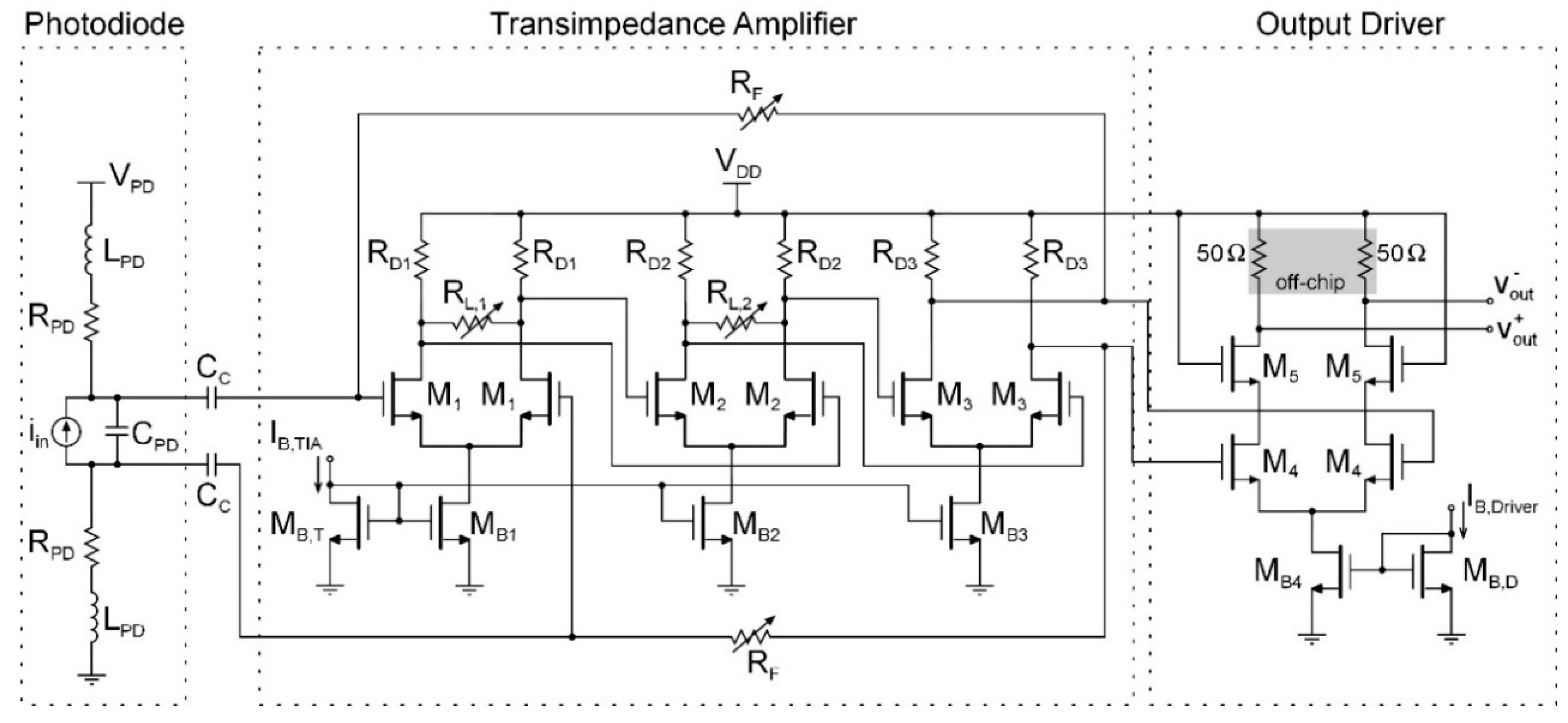
One of the main advantages of IFoF is the lower performance requirement of the photonic devices. Nevertheless, the RAU must present low noise and a very high linearity to achieve a low EVM level. Accordingly, the O/E front-end must be able to satisfy these performance requirements. The main focus of this work is the design of the O/E front end, including a new low-noise transimpedance amplifier with a fully differential implementation to achieve better linearity, using an external 1550 nm PIN photodiode. With the IFoF scheme, the BW requirement and the tradeoff between sensitivity and power consumption is relaxed, so the complexity of the design of the TIA is reduced.
The proposed TIA, shown in Figure 3, is aimed for short-range wireless transmission with an input IF signal at 100 MHz, and it has been designed and fabricated with 65 nm RF CMOS technology. The main purpose of the design is to achieve a reliable transmission of an 802.11a 54 Mb/s WLAN data signal at 5 GHz, which is a multi-carrier OFDM standard that uses 64 QAM modulation.
The PD receives the input optical signal and generates an electrical current, which must be converted to voltage by the transimpedance amplifier, which is the first stage of the analog front end. The TIA is typically one of the most critical modules in an optical receiver. Firstly, since the photogenerated current signal is small, the TIA must show a very low equivalent input noise (EIN) level, as it determines the overall noise of the system. Therefore, the sensitivity of the receiver is mainly determined by the EIN of the TIA.
The TIA must provide a good matching with the PD, which typically presents high parasitics due to the intrinsic junction capacitance, which can be as high as some pF. Therefore, the design of the TIA requires a low input impedance in order to compensate the high PD capacitance to exhibit a wide BW to amplify the incoming signal accordingly. Recent publications report the use of integrated avalanche photodiodes (APDs), which show very low junction capacitances [6,8]. However, these PDs are lacking in linear performance in comparison with PIN PDs. IFoF communications require a very high linearity, as it has a great impact on the EVM. Therefore, in this work, a PIN PD combined with the design of a highly linear TIA are proposed, so that the EVM of the RAU can be maintained at a very low level. The regulated cascode and other open-loop TIA structures based on the common-gate stage have been widely employed in high-speed optical receivers, since they can achieve a high BW with low noise performance. Nevertheless, these topologies show a worse linear behavior, typically not enough for IFoF communications, where linearity is critical to properly transmit the signal. On the other side, closed-loop TIAs, which have been widely used in high-speed optical receivers, can also achieve a wide BW while they present a low EIN and a much better linearity than open-loop configurations [16]. These last two characteristics are mandatory to increase the input dynamic range of the analog front end.
In this work, a shunt–shunt feedback TIA configuration has been employed, as this topology shows a low input impedance and a high linearity, which is the most important characteristic to achieve the best performance for IFoF applications. To improve the system linearity, a differential topology has been chosen, so that second order intermodulation products as well as the effect of supply and substrate noise are strongly reduced [17].
The proposed TIA consists of a differential voltage amplifier and a negative feedback loop. The implementation of the voltage amplifier consists of three cascaded differential pairs and two resistor arrays are employed for the feedback loop. These arrays are digitally programmable to include a gain control of the TIA to increase the input dynamic range of the RAU downlink by varying the transimpedance, R T , which, in a second-order transfer function approximation can be written as:
R T = v o u t + v o u t i i n 2 R F 1 + 2 R F C i n A s + 2 R F C i n A ω A s 2
where R F is the feedback resistor, C i n the total input capacitance, which is dominated by the parasitic capacitance of the photodiode, C P D , and A and ω A are the gain and dominant pole frequency of the core amplifier, respectively. It is a rough approximation, but it is useful to illustrate the proposed frequency compensation mechanism. To achieve high sensitivity, considerably high feedback resistors of the order of several kΩ should be employed to maximize transimpedance. Higher transimpedance results both in higher signal amplification and lower EIN. The dependence of the equivalent input current noise density on the feedback resistor in a differential shunt–shunt feedback TIA can be approximated by the following equation:
E I N 2 2 K B T R F + v n , A 2 ¯ 2 R F 2 ( 1 + 4 ω 2 C i n 2 R F 2 )
where K B is the Boltzmann constant, T the temperature, and ( v n , A 2 ) ¯ the equivalent input noise of the voltage amplifier. It is clear that, according to Equation (2), the higher the R F , the lower the input noise. However, there is an important tradeoff between this parameter and linearity. As the output voltage swing increases, the saturation and the inherent nonlinearities of the CMOS devices start to distort the signal, therefore raising the EVM and shrinking the input dynamic range. As mentioned above, with a digitally programmable feedback resistor, R F (see Figure 4a), the transimpedance can be reduced for large input signals, avoiding saturation as well as nonlinear distortion due to a large output voltage swing, thus extending the input dynamic range.
However, it is well known that the quality factor of the transfer function, Q , which can be derived from Equation (1), depends on the feedback resistor and increases for lower R F values [16]. This might significantly impact the circuit stability as the system becomes underdamped for high Q values, so another control needs to be implemented to keep this factor at lower values. The Q factor, derived from Equation (1) can be approximated by
Q A 2 R F C i n ω A .
Thus, the most direct way to keep Q constant against R F changes is to modify the open-loop gain A proportionally. This gain control is made with the implementation of variable load resistors in the first two differential pairs, R L , i . These resistors, as shown in Figure 4b, consist of a resistor array that is digitally programmable with a 4-bit thermometer-coded digital word, B. Therefore, a simultaneous control of the feedback and the load resistors is made to control both transimpedance and open-loop gain accordingly.
A transistor-level simulation has been carried out with a single control of the feedback resistor to compare the frequency response of the TIA using the double control of both feedback resistor and open-loop gain. As Figure 5 shows, the response without an open-loop gain control shows a frequency peak higher than 4 dB, and the BW increases with lower transimpedance. However, applying the compensation technique, the frequency response is always flat and the BW is almost constant.

3. Experimental Characterization

The proposed circuit has been fabricated in 65 nm CMOS technology using a single voltage supply of 1.2 V. The downlink front end has been designed for an external InGaAs PIN PD, which presents a junction capacitance of approximately 0.45 pF and a 0.85 A/W responsivity at 1550 nm. For measurement purposes, an output driver with 50 Ω output resistance has been implemented to provide a good matching with the measurement instrumentation.
The total RAU downlink area including pads is 2000 × 1150 μm, and the active area of the TIA and the driver is of 115 × 130 μm (see Figure 6).

3.1. Electrical Measurements

To obtain the TIA frequency response, we measure the S21 parameter using a network analyzer (Rohde & Schwarz ZVL 9 kHz-6 GHz). As shown in Figure 7a, the range of programmability with the integrated 4-bit thermometer-coded control of the transimpedance covers up to a 16 dB variation, with a linear-in-dB control from 60 to 76 dBΩ in 4 dB steps. The simultaneous double control avoids frequency response peaking at low transimpedance. Linearity measurements have been carried out using the demodulation of a 54 Mb/s 64 QAM signal at 100 MHz.
Figure 7b shows the measured EVM versus the equivalent input optical power of the signal, at each transimpedance state. The electrical measurements have been performed using a vector signal generator (VSG, Rohde & Schwarz SMW200A) and analyzer (VSA, Keysight M9391A). The TIA presents an EVM lower than 2% for an input RF power range of 40 dB, from −60 to −20 dB, which corresponds to an optical input of −16 to +4 dBm. Noise simulations have been made to take into account only the TIA noise, which exhibits an EIN of 2   pA / Hz . The power consumption of TIA alone is 6 mW.

3.2. Optical Characterization

The experimental set-up for optical data transmission is shown in Figure 8. At the transmitter side, the VSG generates the 54 Mb/s 802.11a WLAN signal at 100 MHz, whose spectrum is shown in Figure 9a. The electrical IF signal is then converted to an optical signal by an electro-optical modulator (Keysight M9403B). This latter module consists of a laser diode with a 1550 nm wavelength, externally modulated by the input IF signal and provides an optical signal with an optical power of 5 mW. The laser is then directly coupled to a 2 m MMF. The MMF is coupled to the InGaAs PD (PDINCF070SC21 M 0), which is connected to the TIA input. To avoid damages to the PD due to the high output power of the laser, a 10 dB optical attenuator is added to the set-up. Finally, a balun is used at the output to convert the differential signal into single-ended for the VSA input, where the output signal, shown in Figure 9b, is received.
The frequency response is measured using the transmission of a continuous wave. The overall link gain from the VSG to the VSA is shown in Figure 10a for each gain configuration. The BW is substantially reduced with respect to the electrical characterization, mainly due to the high parasitic capacitance of the PD. Nevertheless, it is almost constant around 300 MHz with an attenuation lower than 1 dB at 100 MHz and the 16 dB linear in dB transimpedance control is achieved with no frequency peaking, thanks to the simultaneous control of the feedback resistor and the open loop gain. Linearity measurements are carried out using the demodulation of an 802.11a 54 Mb/s transmission using 64 QAM modulation at 100 MHz. The measured EVM results are shown in Figure 10b as a function of the RF power at the output of the VSG, for each transimpedance configuration. The results show an EVM lower than 2% for a 10 dB optical power range and lower than 3% for a 20 dB optical power range.
The main measurement results for the proposed IFoF RAU are summarized in Table 1 with a comparison to recently published TIAs for RoF and IFoF applications. Despite the differences on the frequency of operation of these applications, to make a fair comparison of the performance, we define a figure of merit (FoM):
FoM = Transimpedance   ( Ω ) · BW   ( GHz ) Power   Consumption   ( mW ) .
As shown in Table 1, the TIAs aimed for IFoF achieve a much better FoM than those designed for RoF applications, mainly due to the higher transimpedance and the lower power consumption. The FoM of the other TIA for IFoF [18] is slightly higher than the one achieved in this work. However, it shows simulation results and for linearity measurements it only reports the OIP3 at the maximum transimpedance, with no information about the EVM. Moreover, in [18], only the linearity results at the highest transimpedance are reported, so it does not guarantee good linearity at lower gain configurations. In this work, we present the first IFoF TIA with a linear in dB gain control that is able to extend the input dynamic range for which high linearity is achieved. It shows a better linear performance than RoF receivers, as our proposal achieves an EVM lower than 2% through a wider input dynamic range of 10 dB optical power, compared to the 3 and 5 dB ranges reported in [6] and [8], respectively. Another advantage of this design is the adaptability of its response to higher input capacitances by adjusting the transimpedance and open-loop gain. This design is compatible with commercially available external PIN photodiodes, which can present a much higher junction capacitance, of the order of pF, compared to the greatly low 35 fF and 140 fF capacitances of the integrated PD presented in [8] and [9], respectively.

4. Conclusions

A highly linear low-noise differential TIA to be used in IFoF RAUs has been presented in this paper. The front end has been designed in 65 nm RF CMOS technology with a 1.2 V voltage supply. The proposed design performs a 16 dB linear-in-dB gain control using a method through which the stability is ensured with a simultaneous control of transimpedance and open-loop gain. The TIA achieves an almost constant −3 dB cut-off frequency of 300 MHz and attenuation lower than 1 dB at 100 MHz in all gain configurations. The proposed TIA achieves a 20 dB and 10 dB input optical range with an EVM lower than 3% and 2%, respectively. The lower input noise current density and EVM of the proposed TIA are superior to those reported in recently published works, also with a much lower power consumption achieved with the proposed design. The IFoF scheme presents a high potential and several advantages over RoF, being a good alternative to lower the costs and improve the performance of cost-effective fiber-wireless distributed antenna systems.

Author Contributions

G.R., C.A., and S.C. contributed to the design of the proposed topology; G.R. performed the simulations, the layout design, and the complete experimental characterization of the system; all authors contributed to the data analysis and the writing of the paper.

Acknowledgments

This work has been partially supported by MINECO-FEDER (TEC2014-52840-R and TEC2017-85867-R) and the MINECO fellowship program to Guillermo Royo (BES-2015-073748).

Conflicts of Interest

The authors declare no conflict of interest.

References

  1. Gomes, N.J.; Nkansah, A.; Wake, D. Radio-over-MMF techniques—Part I: RF to microwave frequency systems. J. Lightwave Technol. 2008, 26, 2388–2395. [Google Scholar] [CrossRef]
  2. Koonen, A.M.J.; Larrodé, M.G. Radio-over-MMF techniques—Part II: Microwave to millimeter-wave systems. J. Lightwave Technol. 2008, 26, 2396–2408. [Google Scholar] [CrossRef]
  3. Kumar-Vyas, A.; Agrawal, N. Radio over fiber: Future technology of communication. Int. J. Emerg. Trends Technol. Comput. Sci. 2012, 1, 233–237. [Google Scholar]
  4. Lim, C.; Nirmalathas, A.; Bakaul, M.; Gamage, P.; Lee, K.L.; Yang, Y.; Novak, D.; Waterhouse, R. Fiber-wireless networks and subsystem technologies. J. Lightwave Technol. 2010, 28, 390–405. [Google Scholar] [CrossRef]
  5. Lethien, C.; Loyez, C.; Vilcot, J.-P. Potentials of radio over multimode fiber systems for the in-buildings coverage of mobile and wireless LAN applications. IEEE Photonics Technol. Lett. 2005, 17, 2793–2795. [Google Scholar] [CrossRef]
  6. Yoon, J.S.; Kang, H.S.; Lee, M.J.; Park, K.Y.; Choi, W.Y. CMOS integrated optical receivers for radio-over-fiber transmission of IEEE 802.11g WLAN signals. In Proceedings of the Asia-Pacific Microwave Photonics Conference, Beijing, China, 22–24 April 2009. [Google Scholar]
  7. Kang, H.S.; Lee, M.J.; Choi, W.Y. Low-cost multistandard radio-over-fiber downlinks based on CMOS-compatible Si avalanche photodetectors. IEEE Photonics Technol. Lett. 2009, 21, 462–464. [Google Scholar] [CrossRef]
  8. Ko, M.; Lee, M.J.; Rücker, H.; Choi, W.Y. Silicon photonics-wireless interface ICs for micro-/millimeter-wave fiber-wireless networks. Opt. Express 2013, 21, 22962–22973. [Google Scholar] [CrossRef] [PubMed]
  9. Deshours, F.; Alquié, G.; Abib, G.I.; Grard, E.; Rodrigues, V.; Leclerc, E. Optical transimpedance receiver for high data transmission in OFDM modulation format. J. Lightwave Technol. 2015, 33, 2004–2011. [Google Scholar] [CrossRef]
  10. Pu, T.; Fang, T.; Zheng, J.; Huang, L. Dispersion compensation methods for radio over fiber system. In Proceedings of the 14th International Conference on Optical Communications and Networks, Nanjing, China, 3–5 July 2015. [Google Scholar]
  11. Miyauchi, M.; Kimura, K.; Tsutsumi, Y.; Maeda, J. Compensation of modulation distortion in microwave radio-over-fiber systems using chromatic dispersion. In Proceedings of the International Topical Meeting on Microwave Photonics, Paphos, Cyprus, 26–29 October 2015. [Google Scholar]
  12. Qi, X.; Liu, J.; Zhang, X.; Xie, L. Fiber dispersion and nonlinearity influences on transmissions of AM and FM data modulation signals in radio-over-fiber system. IEEE J. Quantum Electron. 2010, 46, 1170–1177. [Google Scholar] [CrossRef]
  13. Maeda, J.; Katoh, T.; Ebisawa, S. Effect of fiber dispersion on subcarrier QAM signal in radio-over-fiber transmission. J. Lightwave Technol. 2012, 30, 2625–2632. [Google Scholar] [CrossRef]
  14. Royo, G.; Sánchez-Azqueta, C.; Aldea, C.; Celma, S.; Gimeno, C. Highly-linear transimpedance amplifier for remote antenna units. In Proceedings of the International Symposium on Circuits and Systems, Florence, Italy, 27–30 May 2018. [Google Scholar]
  15. Royo, G.; Martínez-Pérez, A.D.; Sánchez-Azqueta, C.; Aldea, C.; Celma, S. Low-EVM CMOS transimpedance amplifier for intermediate frequency over fiber. In Proceedings of the Latin American Symposium on Circuits and Systems, Puerto-Vallarta, Mexico, 25–28 February 2018. [Google Scholar]
  16. Razavi, B. Transimpedance amplifiers. In Design of Integrated Circuits for Optical Communications; McGraw-Hill: New York, NY, USA, 2003; pp. 89–97. [Google Scholar]
  17. Royo, G.; Sánchez-Azqueta, C.; Aldea, C.; Celma, S.; Gimeno, C. CMOS transimpedance amplifier with controllable gain for RF overlay. In Proceedings of the 12th Conference on Ph.D. Research in Microelectronics and Electronics, Lisbon, Portugal, 27–30 June 2016. [Google Scholar]
  18. Ahmad, W.; Abdulaziz, M.; Törmänen, M.; Sjöland, H. CMOS adaptive TIA with embedded single-ended to differential conversion for analog optical links. In Proceedings of the International Symposium on Circuits and Systems, Lisbon, Portugal, 24–27 May 2015. [Google Scholar]
Figure 1. Scheme of a distributed antenna system (DAS) fed by multi-mode fiber (MMF) for indoor networks.
Electronics 08 00437 g001
Figure 2. Conceptual scheme of the downlink of remote antenna units for (a) baseband over fiber, (b) radio over fiber, and (c) intermediate-frequency over fiber.
Electronics 08 00437 g002
Figure 3. Transistor-level topology of the proposed low-noise transimpedance amplifier (TIA) for the remote antenna unit (RAU) downlink. An output driver is included for measurement purposes.
Electronics 08 00437 g003
Figure 4. Implementation of the 4-bit programmable resistor arrays (a) feedback resistor, R F , and (b) load resistors, R L , i .
Electronics 08 00437 g004
Figure 5. Frequency response of the TIA with simultaneous gain control (solid line) and single feedback resistor control (dashed line).
Electronics 08 00437 g005
Figure 6. Layout of the active area of the transimpedance amplifier and the output driver.
Electronics 08 00437 g006
Figure 7. (a) Overall link frequency response and transimpedance of the TIA and (b) measured error vector magnitude (EVM) as a function of the input RF power for each transimpedance configuration. Data from [14].
Electronics 08 00437 g007
Figure 8. Schematic diagram of the experimental set-up for optical data transmission.
Electronics 08 00437 g008
Figure 9. (a) Input spectrum of the integrated optical receiver with f c = 100 MHz. (b) Output spectrum of the integrated transimpedance amplifier.
Electronics 08 00437 g009
Figure 10. (a) Frequency response of the electro-optical front end. The BW is maintained almost constant at around 300 MHz and (b) output signal error vector magnitude using the demodulation of a 54 Mb/s 802.11a WLAN signal.
Electronics 08 00437 g010
Table 1. Summary of measurement results and comparison with RF transimpedance amplifiers.
Parameter[6][8][9][18] **This Work
RAU ArchitectureRoFRoFRoFIFoFIFoF
Technology130 nm CMOS180 nm CMOS150 nm PHEMT65 nm RF CMOS65 nm RF CMOS
Photodiode TechnologyIntegrated APDIntegrated APDExternal PINIntegrated PDExternal PIN
Supply Voltage1.2 V1.8 V5 V1.2 V1.2 V
Transimpedance54 dBΩ62 dBΩ46 dBΩ51–73 dBΩ60–76 dBΩ
Linear-in-dB
Frequency of operation2.5 GHz5.2–5.8 GHz12 GHz550 MHz300 MHz
Input Noise Current DensityN/A 7.3   pA / Hz 26   pA / Hz 3.4   pA / Hz 2   pA / Hz **
EVM3.89%2.5%3%N/A2%
Total Power Consumption18 mW156 mW *100 mW4.8 mW6 mW
FoM   ( Ω · GHz / mW ) 7047 *24511315
* Including output buffer; ** Simulation results.

