


Abstract
Embedded Field-Programmable Gate Array (FPGA)-Advanced RISC Machine (ARM) systems used in industrial and Internet of Things (IoT) environments increasingly operate as network-connected edge devices. While such connectivity enables distributed processing and remote monitoring, it also exposes embedded vision nodes to security threats, including command injection, frame replay, data tampering, and abnormal communication traffic. This paper presents a hardware-assisted security architecture for an FPGA-ARM embedded vision system designed for high-speed image acquisition and network streaming. The proposed solution integrates several lightweight protection mechanisms directly into the FPGA processing pipeline, including frame replay detection, cyclic redundancy check (CRC)-based frame integrity verification, frame sequence monitoring, authenticated command execution, communication anomaly monitoring, and hardware-rooted trust primitives, such as a ring-oscillator physical unclonable function (PUF) and a pseudo-random generator. Optional secure communication is provided via a lightweight ASCON-authenticated encryption core. The architecture was implemented on a Cyclone V System-on-Chip (SoC) platform using an industrial Camera Link camera and evaluated in a low-latency image-acquisition setup operating at 100 fps, with data throughput exceeding 1 Gbps. Experimental results demonstrate that the proposed security architecture introduces only about 1.6% additional FPGA logic utilization while maintaining full real-time acquisition performance. The presented approach demonstrates that practical hardware-level security mechanisms can be integrated into FPGA-based embedded vision nodes with minimal architectural modifications and negligible performance overhead.
1. Introduction
High-speed embedded vision systems have become an essential component of modern industrial inspection, robotics, intelligent monitoring, and scientific imaging platforms. Such systems frequently operate under strict real-time constraints while processing large volumes of visual data acquired from high-resolution sensors. Field-programmable gate array (FPGA)-based architectures are particularly well suited for these applications because they provide massive parallelism, deterministic latency, and efficient hardware acceleration for image acquisition and processing pipelines [1,2,3]. Recent developments in system-on-chip (SoC) platforms integrating programmable logic with embedded processors further extend these capabilities by enabling tight cooperation between hardware-accelerated processing and software-based control layers [4,5,6]. Such heterogeneous FPGA-ARM platforms are widely used in edge computing environments where low-latency image processing must be combined with networking, data analytics, and remote system management.
In high-performance vision systems, image sensors are often connected to FPGA-based frame-grabber platforms through high-bandwidth interfaces such as Camera Link, CoaXPress, or high-speed serial links. These interfaces allow image acquisition at hundreds of frames per second while generating gigabit-scale data streams that must be processed and transferred with minimal latency. FPGA devices are therefore commonly used to implement real-time acquisition pipelines, buffering architectures, and pre-processing modules before data is forwarded to higher-level processing units [1,4,7]. In recent years, FPGA-based accelerators have also been widely applied to machine vision and autonomous systems, including edge-based object detection and vision processing for autonomous vehicles [5,6].
Traditionally, frame-grabber systems were deployed in isolated environments where the acquisition hardware was directly controlled by a dedicated host computer through local communication interfaces. However, modern industrial infrastructures increasingly integrate embedded vision devices into network-connected cyber–physical systems and IoT ecosystems. In such environments, embedded vision nodes often communicate with multiple workstations, monitoring servers, or cloud-based analytics platforms over Ethernet or wireless networks [1,8]. While this connectivity significantly improves system flexibility and enables distributed data processing, it also introduces new security challenges. Communication channels between the host system and the embedded hardware may become targets of malicious manipulation, unauthorized access, or unintended interference.
Security threats affecting FPGA-based systems have been widely investigated in recent years. Several studies have highlighted vulnerabilities related to configuration bitstream manipulation, hardware Trojans, and physical attacks targeting programmable logic devices [9,10,11,12]. More advanced attack vectors include side-channel analysis, fault injection, and reverse engineering of FPGA-based designs [13,14,15]. The increasing use of FPGAs in multi-tenant cloud infrastructures and distributed edge computing environments has further expanded the attack surface, raising concerns about device trust, data confidentiality, and runtime system integrity [16,17]. Hardware security has therefore become an important research area for modern FPGA-based cyber–physical systems [18,19].
Embedded vision platforms introduce several additional security risks due to the continuous streaming of high-volume sensor data. One possible threat is a replay attack, where previously captured frames are retransmitted to conceal abnormal events or falsify inspection results. Another potential vulnerability is data tampering, where image frames are modified during transmission or storage, leading to incorrect interpretation of measurement results [20]. Systems supporting remote configuration or control may also be exposed to command injection attacks, in which unauthorized commands manipulate acquisition parameters or disrupt system operation. Similar security challenges have been reported in industrial cyber–physical systems and smart manufacturing environments where sensor data integrity and system availability are critical [21,22]. Without dedicated verification mechanisms, such attacks may remain unnoticed, particularly in high-throughput imaging systems operating at hundreds of frames per second.
Traditional security mechanisms are often implemented at the software level in the host system or operating system environment. However, software-only solutions may introduce additional latency and computational overhead when applied to high-speed data streams. Furthermore, if the host system becomes compromised, software-based protection mechanisms may be bypassed entirely. Hardware-assisted security mechanisms implemented directly in FPGA logic provide an alternative approach that enables real-time monitoring of data streams and system behavior without interrupting the processing pipeline. Such approaches include hardware security monitors, cryptographic modules, and hardware-rooted trust primitives implemented within the FPGA fabric [23,24,25,26]. Additional techniques such as physical unclonable functions (PUFs) have also been proposed to provide device-specific authentication and hardware-rooted trust [27,28].
Recent research has explored various hardware security architectures for FPGA-based systems, including runtime self-attestation mechanisms, trusted execution environments, and hardware intrusion detection frameworks [29,30,31]. Lightweight authenticated encryption algorithms such as ASCON have also been proposed for secure communication in constrained embedded and IoT environments [32]. Other studies focus on anomaly detection, authentication protocols, and secure communication frameworks for heterogeneous FPGA-CPU edge devices [25,33,34,35]. Despite these advances, relatively little work has focused on integrating multiple lightweight hardware security primitives directly into low-latency embedded vision pipelines while maintaining minimal resource overhead and preserving deterministic acquisition performance.
To address this gap, this work proposes a hardware-assisted security architecture for FPGA-ARM embedded vision systems operating in network-connected environments. The proposed approach integrates several lightweight monitoring and protection mechanisms directly into the FPGA acquisition and communication pipeline. The architecture is implemented on a Cyclone V SoC platform and combines high-speed Camera Link image acquisition, frame buffering, and network streaming with hardware-level security monitoring modules designed to protect both the image data stream and the system control interface.
This work makes the following contributions:
- A pipeline-integrated security design paradigm for FPGA-based vision systems, where security mechanisms are embedded directly into the streaming data path rather than implemented as external or software-managed modules.
- A formalized mapping between attack classes (replay, tampering, control injection, and flooding) and corresponding hardware-level detection mechanisms, enabling systematic coverage of both data-path and control-path threats.
- A quantitative evaluation framework for embedded vision security, introducing measurable metrics such as detection rate, false positive rate, and detection latency under adversarial conditions.
- An experimental demonstration showing that full-stream security monitoring can be achieved with negligible performance overhead (1.6% logic utilization, zero throughput degradation) while maintaining deterministic real-time operation at 1 Gbps.
Unlike prior work focusing on isolated mechanisms or software-assisted protection, this work demonstrates that security can be treated as an intrinsic property of the streaming architecture rather than an external add-on.
2. Related Work
Networked FPGA–ARM embedded vision systems sit at the intersection of high-throughput streaming data paths, remote control interfaces, and resource-constrained edge devices. Prior work, therefore, spans FPGA-specific trust and threat models, IoT and sensor network security, and hardware-assisted monitoring and cryptography. This section summarizes, for each class of threat listed in Table 1, how such threats arise in practice and which classes of countermeasures appear in the literature, in line with systematic and survey treatments of FPGA vulnerabilities and mitigations [9,10,11,12,16,17,18,19].
Table 1.
Security threats and corresponding hardware protection modules.
2.1. Replay Attacks, Timing Manipulation, and Stream Ordering
In streaming and control channels, an adversary may capture legitimate frames or commands and re-inject them later (replay), stretch or compress inter-arrival times (timing manipulation), or disturb ordering so that the receiver processes stale or duplicated content. Bitstream- and system-level discussions of FPGA deployments explicitly note replay of prior vulnerable configurations as a concern [9]. In IoT and sensor contexts, replay is a standard attack pattern alongside man-in-the-middle and jamming-style effects [8]. Lightweight authenticated encryption can provide confidentiality and authenticity but, by itself, may not distinguish legitimate retransmissions from malicious replays of ciphertext [32].
Defenses include strict sequence or freshness checks (counters, expected frame indices, timing windows), and cryptographic freshness such as nonces or session keys bound to monotonic state. Hardware-oriented work on ASCON for IoT combines AEAD with replay detection using nonce tracking (e.g., Bloom-filter-based freshness verification at decryption) so that duplicated messages are rejected [32]. Monotonic time or counter references address temporal spoofing, where an attacker replays old material or skews perceived time; these align with secure protocol design and hardware-supported timestamp or counter generation [18,32]. At the architectural level, hardware security monitoring that binds integrity checks to real-time execution can complement stream-level validation [23].
2.2. Data Corruption, Tampering, and Loss of Integrity
Integrity failures may be accidental (noise, EMI) or malicious (on-path bit flips, interface manipulation, trojaned logic). Untrusted IPs and supply-chain risks motivate concern about hardware Trojans (HTs) that alter on-chip traffic or functionality [10,20]. Communication tampering in interconnect-centric systems is a recognized HT effect (e.g., malicious modification of flits in NoC-based designs) [20]. Vision and AI pipelines face image-data tampering at the sensor interface or in software, which can change downstream decisions [28]. Embedded programs are also subject to data- and control-flow tampering (e.g., via vulnerabilities or malicious components) [23].
Checksums and MACs are widely used for fast detection of corruption; cryptographic MACs and AEAD additionally bind authenticity to a secret key [25,28,32]. Image-sensor work combines PUF-derived keys with MAC verification in a trusted execution environment to detect tampering [28]. For CPU–FPGA heterogeneous edges, frameworks such as SecureComm illustrate confidentiality and integrity of DDR-mediated transfers using block ciphers plus message authentication [25]. Hardware monitoring architectures that track data integrity (and, in combination, control-flow integrity) aim to detect tampering-style attacks at runtime with bounded overhead [23]. ML-assisted tampering detection in on-chip networks illustrates monitoring distributed traffic for malicious modification [20]. Broader surveys of connected hardware emphasize side-channel and fault attacks as complementary threats to integrity [13,14,18], motivating layered defenses beyond a single checksum.
2.3. Unauthorized Control, Impersonation, and Weak Entropy
Remote configuration and command paths are vulnerable to forgery and impersonation if endpoints cannot be authenticated or if session material is predictable. Protocol literature for constrained domains analyzes impersonation, forgery, and key-compromise scenarios [33]. PUFs exploit manufacturing variability to derive device-specific secrets and support authentication without permanent secret storage in the same form [18,27]. Pseudo-random or weak RNGs undermine nonces, session tokens, and challenge–response protocols; surveys on hardware security and IoT stress robust entropy sources and key provisioning [18,19].
Mutual authentication and key agreement protocols, often with formal verification, establish shared keys for later MAC/AEAD use; implementations on FPGA SoCs demonstrate feasibility for embedded real-time use [33]. Multi-factor or layered authentication (e.g., symmetric plus asymmetric primitives) appears in FPGA-oriented authentication schemes for embedded applications [34]. PUF-based designs on FPGA improve area/speed and robustness trade-offs for hardware-rooted identities [27]. HSM-centric architectures for industrial IoT summarize how tamper-resistant cryptography and trusted execution anchor secure communication and key management [24], relevant when control and telemetry must meet higher assurance. Runtime attestation of FPGA-based IoT devices addresses trust in loaded logic and configuration [29], while TEE-style secure execution on FPGA SoCs addresses isolation between software and programmable logic [30].
2.4. Availability: Flooding, Denial-of-Service, and Anomalous Traffic
Attackers may exhaust buffers, bandwidth, or processing with high-rate or malformed traffic, or may cause denial-of-service conditions in interconnects; NoC-oriented security summaries explicitly list DoS (alongside spoofing and extraction-style issues) as HT-related risks [20]. In FPGA cyber–physical settings, anomaly detection is used to flag deviations from expected configuration or behavior [22].
Rate limiting, traffic monitoring, and anomaly detection, including learning-based detectors for unusual bitstream or traffic patterns, support availability, and early warning [22]. Distributed monitoring of on-chip communication can localize sources of tampering or abnormal traffic [20]. At the system level, hybrid security for communication-centric FPGA platforms (e.g., NoC-oriented schemes) illustrates defense-in-depth for interconnected accelerators [31].
2.5. FPGA Bitstream, SoC Attack Surface, and Monitoring
Although Table 1 focuses on runtime vision-pipeline threats, FPGA SoC literature emphasizes bitstream confidentiality and integrity, side channels, and fault injection as foundational concerns [9,10,11,12]. SoC FPGA devices enlarge the attack surface, where a software flaw may expose the FPGA fabric or configuration path [12]. Power side-channel monitoring serves as an example of hardware-assisted supervision [26]. Man-at-the-end and reverse-engineering threats matter when devices are physically exposed [15]. Multi-tenant and cloud FPGA settings add co-tenancy and sharing risks [16,17]. These bodies of work motivate lightweight, pipeline-local protections for real-time vision (sequence checks, CRC/MAC, authenticated commands, PUF, PRNG, AEAD) as complementary to vendor bitstream protection and supply-chain assurance.
2.6. Positioning of This Work
Prior surveys and systematic reviews provide broad vulnerability, mitigation mappings for FPGAs and IoT hardware [11,18,19]. Works on heterogeneous CPU, FPGA security [25], PUFs [27], AEAD with replay handling [32], integrity monitoring [23], HSM-backed IIoT [24], and FPGA anomaly/tampering detection [20,22] collectively cover the building blocks reflected in Table 1. The gap addressed here is the co-integration of multiple such mechanisms directly in a high-throughput Camera Link vision pipeline on an FPGA–ARM SoC with minimal added logic, which is not the focus of most single-threat or cloud-centric studies [16,17].
Unlike prior work that treats security as an independent module or software-managed layer, this work introduces a pipeline-native security architecture in which protection mechanisms are embedded directly into the streaming dataflow. This enables continuous, deterministic, and non-blocking security verification without additional buffering or processing stages. The key insight is that security can be modeled as a dataflow property of the system rather than a separate functional layer. This approach allows security guarantees to scale with throughput while preserving real-time constraints, which is critical for high-speed embedded vision systems.
3. Materials and Methods
3.1. Hardware Setup
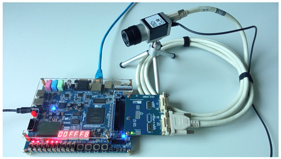
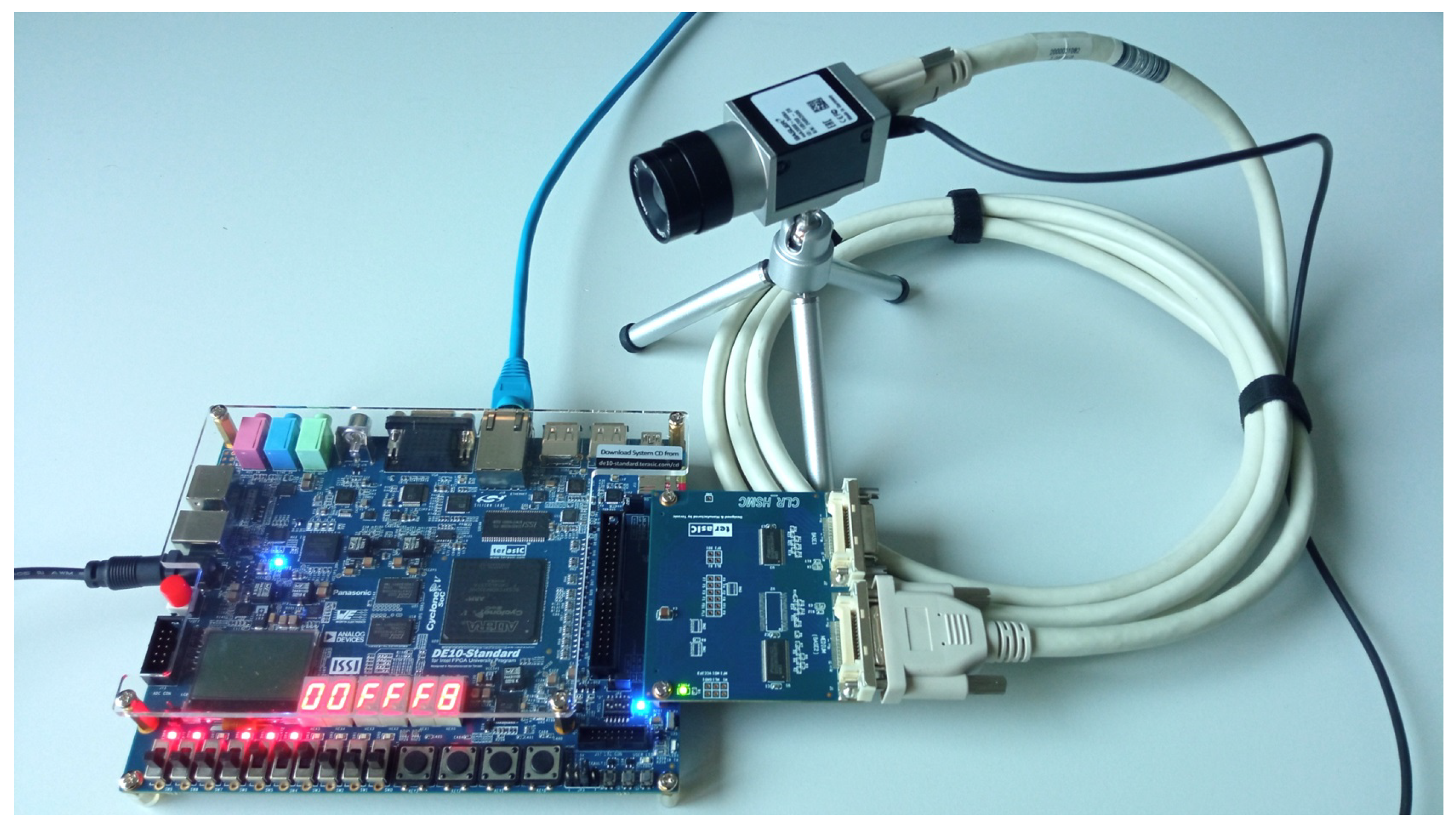
The experimental hardware setup used for the evaluation of the proposed system is shown in Figure 1. The prototype is implemented on a DE10-Standard development board (Terasic Technologies Inc., Hsinchu City, Taiwan) equipped with an Intel Cyclone V SoC FPGA (Intel Corporation, Santa Clara, CA, USA), which integrates programmable logic and an ARM-based processing system. Image acquisition is performed using a Basler ace acA2000-340kc industrial Camera Link camera (Basler AG, Ahrensburg, Germany) connected to the FPGA board through a Camera Link interface module. The camera provides a maximum resolution of 2048 × 1088 pixels (approximately 2 MP) with a pixel size of 5.5 m × 5.5 m. In the used configuration, the camera operates via the Camera Link Base interface and is capable of delivering image streams at frame rates of up to 340 frames/s at full resolution with 10-bit pixel depth, utilizing dual 26-pin SDR connectors. The FPGA receives raw pixel data from the camera, performs real-time processing, and buffers it to the external RAM. The captured frames are then accessed by the embedded ARM processor via the AXI interconnect for further processing and communication with a host computer.
Figure 1.
Experimental edge vision node consisting of a Cyclone V SoC FPGA frame-grabber and an industrial Camera Link camera used for evaluation of the proposed hardware-assisted security architecture.
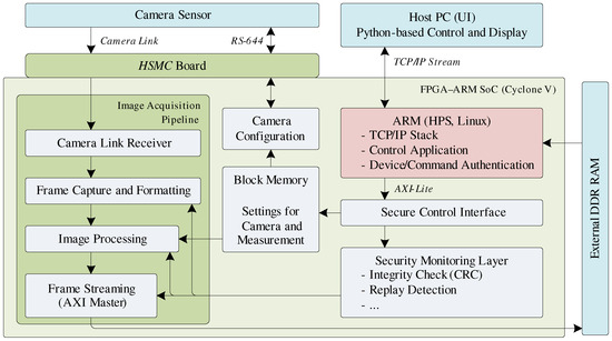
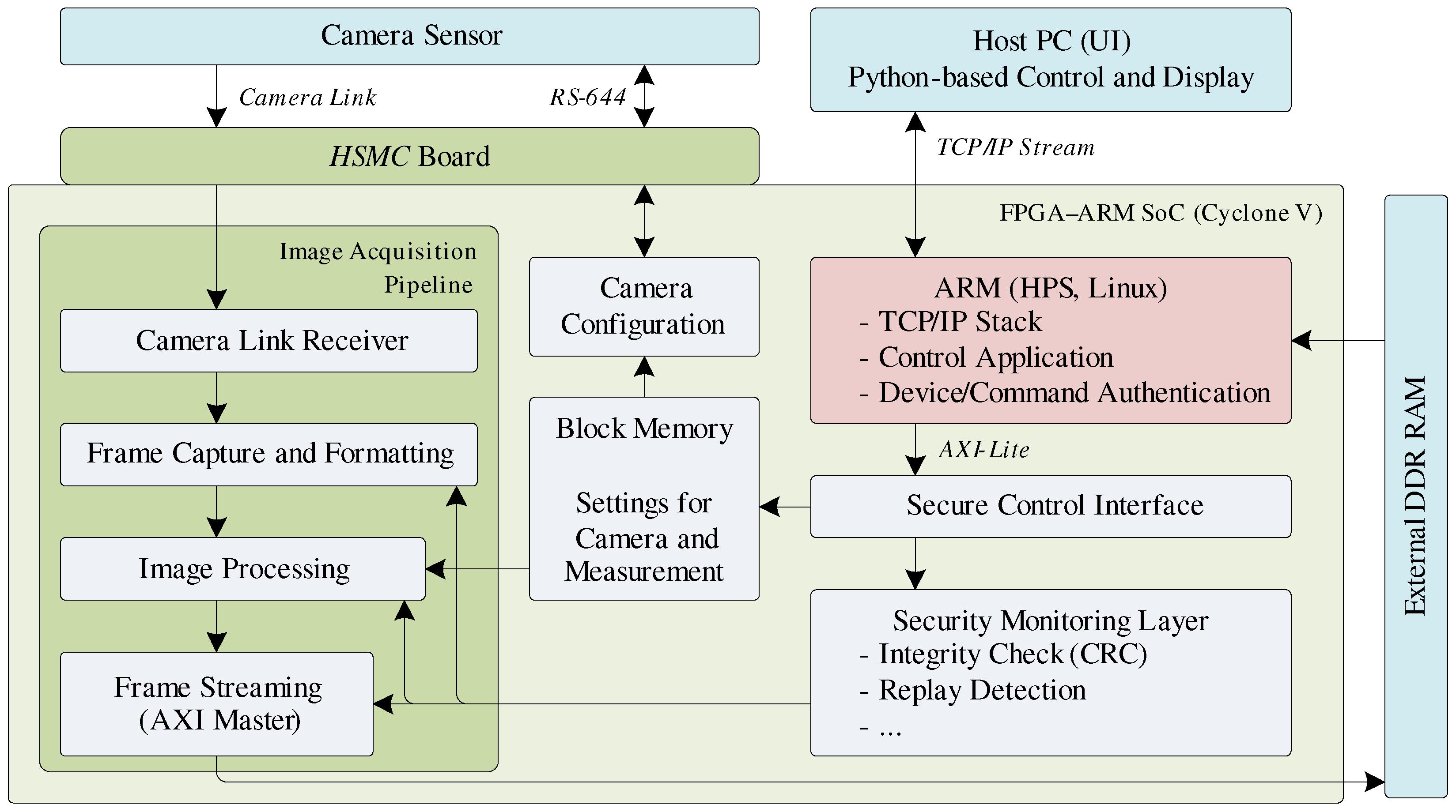
Figure 2 presents the structural block diagram of the proposed SoC-based embedded vision system. The architecture combines high-speed image acquisition, real-time hardware processing, security monitoring, and network communication within a single FPGA–ARM system-on-chip platform. The system is organized around a Cyclone V FPGA device integrating programmable logic and an embedded ARM hard processor system (HPS), enabling efficient cooperation between hardware acceleration modules and software-based control functions.
Figure 2.
Structural block diagram of the SoC-based vision system.
Image acquisition is performed using an industrial camera connected through the Camera Link interface. The camera sensor generates a continuous pixel stream that is transmitted via the Camera Link physical layer (RS-644 signaling) to the Camera Link receiver implemented in the FPGA fabric. The receiver decodes the serialized camera data and reconstructs the pixel stream together with synchronization signals such as line valid and frame valid. The decoded data is then passed to the frame capture and formatting module, which organizes the incoming pixel stream into structured image frames suitable for further processing.
After frame capture, the image data is forwarded to the image processing stage implemented in the FPGA logic. This stage may perform lightweight preprocessing operations or formatting required for further processing and storage. The processed frame data is written to the external DDR memory connected to the FPGA. The external memory serves as a frame buffer that temporarily stores captured images and allows asynchronous access by other system components.
Data transfers between the programmable logic and the processor subsystem are performed through the AXI-based interconnect. The FPGA implements an AXI master interface responsible for streaming frame data to the external DDR memory. The embedded ARM processor running Linux can subsequently access the stored frames through the shared memory subsystem for further processing or transmission. The ARM subsystem also implements the TCP/IP network stack and a control application that manages communication with the host computer.
The host PC interacts with the embedded vision system through an Ethernet network connection. A Python 3.12.9-based application running on the host provides a user interface for system control, configuration, and image visualization. Captured frames are transmitted from the embedded system to the host using a TCP/IP data stream, enabling remote monitoring and processing of the acquired images.
System configuration and camera control are handled through a dedicated secure control interface implemented in the FPGA. This interface allows the ARM processor or the host system to configure various camera sensor parameters required for image acquisition. The configurable parameters include exposure time, horizontal and vertical image offsets (Offset X/Y), image width and height, vertical and horizontal decimation factors, and optional horizontal or vertical image mirroring (Reverse X/Y). In addition, the interface provides control over the frame acquisition trigger mode and the programmable trigger delay used for synchronization with external events. All configuration parameters are stored in memory-mapped block memory registers within the FPGA, allowing fast and deterministic access to camera and measurement settings during system operation.
3.2. Security Modules
To improve the robustness and trustworthiness of the proposed embedded vision system, a set of lightweight hardware security modules was implemented directly in the FPGA logic (Table 1). These modules operate alongside the image acquisition and processing pipeline and provide monitoring and protection of both the frame data stream and the system control interface. The modules were designed to introduce minimal computational and hardware overhead so that the high data throughput required by the Camera Link acquisition system is preserved while improving the security properties of the platform.
A replay and timing attack detector was implemented to monitor the temporal consistency of the incoming frame stream. The module receives the frame identifier and frame valid signal generated during frame capture and compares the current frame identifier with the previously processed value. If the received frame identifier is smaller than or equal to the previous identifier, a replay event is detected. In addition, the time interval between consecutive frames is measured using the system clock. If the measured interval falls outside predefined limits, a timing anomaly flag is generated. This mechanism allows detection of duplicated frames, delayed frames, or artificially injected frames that may indicate a replay or manipulation attempt.
To ensure the integrity of frame data flowing through the processing pipeline, a lightweight CRC-32 integrity verification module was implemented. The module operates in a streaming mode and processes incoming data bytes sequentially as they pass through the FPGA. During frame reception, the CRC value is continuously updated, and the final checksum is produced at the end of the frame. The calculated checksum can then be compared with an expected value in order to detect accidental data corruption or intentional modification of the frame contents.
A frame sequence monitoring module was also introduced to verify that frames arrive in the expected order. The module maintains an internal expected frame counter and compares it with the received frame identifier. If the received identifier equals the expected value, the frame sequence is considered valid. If the identifier is smaller than the expected value, an out-of-order or duplicated frame is detected. If the identifier is larger than expected, a frame loss condition is reported. This mechanism allows reliable monitoring of frame continuity in high-speed acquisition systems.
The system allows configuration and control commands to be sent from the host computer to the embedded platform through the network interface. To prevent unauthorized modification of acquisition parameters, a hardware command-authentication mechanism was implemented in the FPGA. Each command packet contains a command identifier, a parameter value, and an authentication token. The FPGA recomputes the expected authentication token using a predefined secret key combined with the command identifier and parameter value. If the received token does not match the expected value, the command is rejected and ignored by the system.
To ensure reproducibility of the proposed design, the configuration parameters of the implemented hardware security primitives are explicitly defined. The ring oscillator PUF is implemented using independent ring oscillators constructed from LUT-based inverter loops. The oscillation frequencies are measured using 16-bit counters over a fixed observation window of 50,000 system clock cycles. The final PUF response is generated through pairwise comparison of oscillator frequencies, resulting in an 8-bit response vector per evaluation. The selected number of oscillators represents a trade-off between hardware overhead and response entropy, as increasing the number of oscillators improves uniqueness and reliability but also increases logic utilization. The chosen configuration is consistent with lightweight FPGA-based PUF implementations targeting resource-constrained embedded systems while providing a higher number of challenge-response pairs compared to minimal configurations.
The pseudo-random number generator is implemented as a 32-bit linear feedback shift register (LFSR) using a primitive feedback polynomial defined by taps at positions . This configuration produces a maximal-length sequence with a period of , ensuring adequate statistical properties for non-cryptographic applications such as nonce generation and session identifiers. A fixed non-zero initialization seed (0xACE1ACE1) is used to ensure deterministic behavior and avoid lock-up conditions. The 32-bit LFSR length was selected as a compromise between statistical quality and hardware efficiency, as shorter LFSRs provide insufficient period length, while longer registers increase resource usage without significant benefit for the intended application scope.
To justify the selection of the implemented hardware primitives, alternative design options were considered for both device authentication and random number generation. For device impersonation protection, physical unclonable functions (PUFs) provide a hardware-rooted identity derived from intrinsic process variations. Among common PUF architectures, including arbiter-based, memory-based (e.g., SRAM PUF), and ring oscillator (RO) PUFs, the RO-based approach was selected due to its suitability for FPGA implementation. Arbiter PUFs typically require carefully balanced delay paths and are sensitive to routing asymmetries and metastability, which can be difficult to control in FPGA fabrics. Memory-based PUFs, while offering strong entropy, rely on specific memory primitives and startup conditions that may not be consistently accessible or controllable across different FPGA configurations. In contrast, RO-PUFs can be efficiently realized using standard lookup tables and routing resources, as demonstrated in the implemented design, and provide stable and repeatable responses through frequency comparison over a measurement window. Additionally, RO-PUFs exhibit good robustness to environmental variations when sufficient averaging is applied, making them well-suited for lightweight, reproducible device fingerprinting in embedded FPGA systems.
For random number generation, the design employs a linear feedback shift register (LFSR)-based pseudo-random number generator instead of reusing the RO-PUF structure as a true random number generator (TRNG). While RO-based TRNGs can provide high-quality entropy derived from jitter and thermal noise, they typically require additional post-processing (e.g., debiasing, entropy extraction) and careful validation to ensure statistical randomness, which increases implementation complexity and resource usage. In contrast, the LFSR-based generator offers a compact, deterministic, and high-throughput solution with minimal logic overhead, making it appropriate for non-cryptographic purposes such as nonce generation, session identifiers, and protocol randomization. Furthermore, separating the roles of PUF (for device identity) and RNG (for protocol support) improves architectural clarity and avoids potential interference between entropy extraction and fingerprint stability. This design choice reflects a trade-off favoring simplicity, reproducibility, and low resource utilization, which are key constraints in high-speed embedded vision systems.
In order to detect abnormal communication behavior, a traffic anomaly monitoring module was integrated into the communication path. The module counts incoming packets within a predefined time window and compares the measured packet rate with a configured threshold value. If the observed rate exceeds the expected limit, an anomaly signal is generated. Such behavior may indicate packet flooding, denial-of-service attempts, or other abnormal activity affecting the embedded system.
For optional secure communication, a lightweight encryption core based on the ASCON authenticated encryption algorithm was implemented. ASCON is a modern, lightweight cryptographic primitive specifically designed for constrained embedded and IoT devices. The encryption module provides confidentiality and integrity protection for transmitted data blocks and can be used to secure communication between the embedded system and the host computer.
A secure timestamp generator was implemented to provide a monotonic time reference for the security monitoring modules. The generator produces a continuously increasing 64-bit timestamp synchronized with the system clock. This timestamp can be used for frame timing verification, replay detection, and security event logging, ensuring consistent temporal ordering of system events.
All described security modules were synthesized and integrated into the FPGA-based processing architecture. Despite the inclusion of multiple protection mechanisms, the resulting hardware overhead remains very small relative to the overall FPGA capacity, demonstrating that practical hardware security mechanisms can be integrated into high-speed embedded vision systems with minimal resource impact.
3.3. Security Architecture Discussion
Unlike conventional modular security designs, the proposed architecture is explicitly co-designed with the streaming data path, ensuring that all protection mechanisms operate inline within the acquisition pipeline rather than as external or post-processing components. The implemented security modules form a multi-layer protection architecture designed specifically for embedded vision systems operating in networked environments. Instead of relying on a single protection mechanism, the system integrates multiple complementary security primitives that address different classes of potential threats.
The first layer focuses on the protection of the real-time frame acquisition and processing pipeline. Modules such as the replay and timing detector, CRC integrity verification unit, frame counter monitor, and secure timestamp generator operate directly on the incoming frame stream. These mechanisms ensure that frame data is received in the correct order, within expected timing constraints, and without corruption. By performing these checks in hardware, security monitoring can be executed in real time without introducing additional latency in the processing pipeline.
The second layer protects the control and communication interfaces of the embedded system. The secure command authentication module verifies that configuration commands originate from an authorized source before applying any changes to system parameters. The traffic anomaly monitor observes communication patterns and detects abnormal packet rates that may indicate denial-of-service attempts or other suspicious behavior. In addition, the ASCON lightweight encryption core enables authenticated encryption of transmitted data, providing confidentiality and integrity protection for communication between the embedded system and the host computer.
The third layer introduces hardware-rooted trust primitives. The ring oscillator physical unclonable function provides a device-unique hardware fingerprint that is used for secure device identification, while the pseudo-random number generator supports cryptographic protocols requiring random values. Together, these components enable hardware-level support for authentication and secure key generation.
By distributing security mechanisms across multiple layers of the architecture, the system achieves a balanced protection model while maintaining low hardware complexity. The post-implementation results demonstrate that the combined overhead of all implemented security modules remains very small relative to the total FPGA resources, confirming that introduced hardware security mechanisms can be integrated into high-speed embedded vision platforms without compromising system performance.
Although the proposed architecture is demonstrated in the context of an embedded vision system, the design principles are not limited to image-based applications. The presented security modules operate on generic streaming data interfaces and control channels, making them directly applicable to other high-throughput FPGA-based systems such as industrial sensor networks, software-defined radio, network packet processing, and edge AI accelerators. In particular, mechanisms such as sequence monitoring, integrity verification, authenticated control, and anomaly detection can be integrated into any deterministic dataflow pipeline. The key requirement is the presence of structured streaming data and timing constraints, which are common in many cyber–physical and real-time embedded systems. Therefore, the proposed co-design approach can be generalized to a broad class of FPGA-based edge devices requiring low-latency, hardware-level security enforcement.
Beyond the specific implementation, the proposed architecture reflects a set of design principles for integrating security into high-throughput FPGA-based streaming systems. Security mechanisms are placed directly in the data path, allowing continuous monitoring without introducing buffering or software intervention. This ensures that detection latency remains bounded and independent of system load. Each identified threat class is mapped to a dedicated hardware primitive, enabling modular coverage of replay, integrity, control, and availability threats. This structured mapping allows the architecture to be extended or adapted to other streaming applications. All security modules operate in parallel with the processing pipeline, ensuring that security scales with data throughput and does not become a bottleneck.
4. Results and Discussion
4.1. Security Modules Investigation
The proposed security architecture integrates several lightweight monitoring and protection modules implemented directly in the FPGA fabric. These modules operate in parallel with the image acquisition and buffering pipeline and therefore do not interfere with the real-time operation of the vision system. The implemented modules include replay and timing detection, frame integrity verification using CRC, frame counter monitoring, command authentication, a ring oscillator-based physically unclonable function, a random number generator, traffic anomaly monitoring, lightweight encryption using the ASCON core, and a secure timestamp generator. Table 2 summarizes the hardware resource utilization and latency of the implemented security modules.
Table 2.
Resource utilization of security modules.
The complete FPGA security architecture introduces an overhead of 678 ALMs and 975 registers. Considering the Cyclone V FPGA capacity of 41,910 ALMs, the proposed security framework increases the overall logic utilization by approximately 1.6%. This demonstrates that introduced hardware-level protection can be achieved with minimal resource overhead. Moreover, the low utilization footprint preserves sufficient resources for integrating additional processing or application-specific modules without compromising system scalability.
In addition to hardware cost evaluation, the functional effectiveness of the security architecture was investigated by emulating several representative attack scenarios in simulation. These experiments evaluate whether the corresponding monitoring modules are capable of detecting abnormal behavior within the image acquisition and control pipeline. The considered scenarios include replayed frames, corrupted data frames, frame loss events, unauthorized control commands, and abnormal command traffic patterns. The detection capability of the implemented modules is summarized in Table 3. The results show that each security mechanism successfully detects the corresponding abnormal condition with minimal detection latency. This confirms that the proposed architecture achieves security-by-design within the streaming pipeline, rather than introducing security as a separate processing stage.
Table 3.
Security attack detection validation.
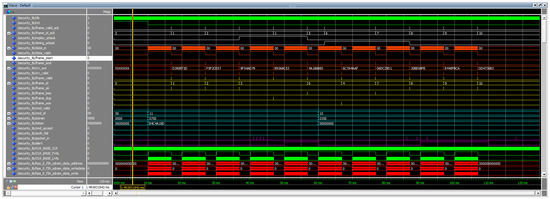
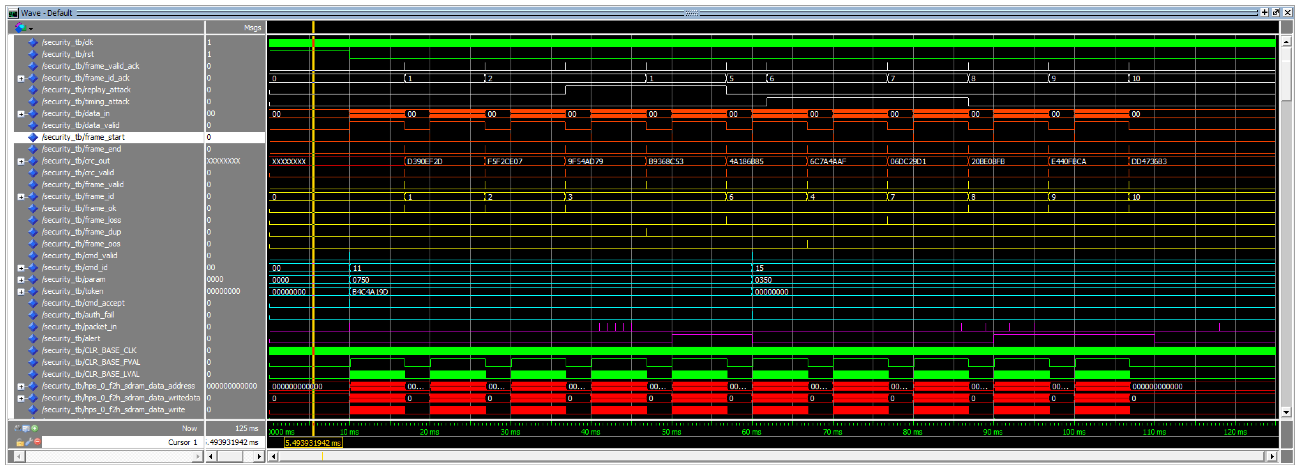
Figure 3 presents a timing simulation of the integrated security architecture using a unified VHDL testbench that combines all implemented protection modules. To improve readability, only the most relevant signals are discussed in the following analysis, while the remaining signals provide timing context for concurrent module operation. The test scenario emulates a continuous, frame-based data stream, along with control commands and network traffic, allowing simultaneous validation of data-path and control-path security mechanisms. The simulation includes both normal operating conditions and intentionally injected anomalies, such as duplicated frame identifiers, missing frames, invalid authentication tokens, and increased packet rates. This approach enables verification of the interaction between modules and demonstrates that all security functions operate concurrently without interfering with the real-time processing pipeline.
Figure 3.
Timing simulation of the integrated hardware security modules summarized in Table 3. The waveform illustrates the concurrent operation of multiple protection mechanisms within a unified testbench. White signals correspond to the replay/timing detector, orange to the CRC-32 integrity module, yellow to the frame counter monitor, cyan to the command authentication module, and magenta to the traffic anomaly monitor. Red traces represent SDRAM interface activity, while green signals denote camera synchronization signals.
The replay/timing detector and frame counter monitor are evaluated using a sequence of frame identifiers with deliberate irregularities. As shown in the waveform, duplicated and out-of-order frame identifiers trigger the replay_attack, frame_dup, frame_loss, and frame_oos signals within a single clock cycle after frame_valid is asserted. In parallel, the CRC-32 module processes the incoming data stream and generates a checksum at each frame boundary. The crc_valid signal indicates the completion of CRC computation, allowing detection of corrupted frames. These results confirm that frame-level integrity, ordering, and temporal consistency are continuously monitored in hardware without introducing additional latency.
The command authentication module is validated by injecting both valid and invalid command tokens. The waveform shows that only correctly authenticated commands result in cmd_accept assertions, while invalid tokens immediately trigger auth_fail, preventing unauthorized configuration changes. Additionally, the traffic anomaly monitor evaluates packet arrival rates within a fixed observation window. During periods of increased packet activity, the packet counter exceeds the predefined threshold, causing the alert signal to be asserted. Results demonstrate that both control-plane security and communication anomaly detection are effectively enforced in real time, complementing the data-path protection mechanisms. All detection signals are generated with deterministic latency (typically one clock cycle), confirming the suitability of the proposed architecture for high-speed embedded vision systems.
Another important aspect is the potential impact of the security modules on the real-time performance of the image acquisition system. Since all monitoring blocks operate in a pipelined or parallel manner, they do not introduce additional delays in the critical image data path. Experimental evaluation confirmed that the overall system throughput and frame acquisition rate remain unchanged when the security modules are enabled. Table 4 summarizes the comparison between the baseline system configuration and the secure architecture. The acquisition configuration used in the experiments corresponds to pixel images with Bayer GB 10-bit depth at a frame rate of 100 fps. This results in an effective raw data throughput of approximately 1.05 Gbps between the Camera Link interface and the FPGA acquisition pipeline. The reported throughput is derived from these acquisition parameters and was verified during continuous real-time operation in the hardware setup. The data stream was monitored to ensure sustained frame transfer at 100 fps without data loss or pipeline stalls, confirming that the system maintains the required throughput under nominal operating conditions.
Table 4.
Impact of security modules on system throughput (camera to FPGA).
The implemented security architecture provides protection against several typical threats relevant to embedded vision systems and industrial imaging applications. The relationship between the considered threats and the implemented hardware mitigation mechanisms is summarized in Table 5. The results demonstrate that the proposed architecture provides layered protection covering data integrity, command authentication, anomaly detection, and cryptographic protection of sensitive communication channels.
Table 5.
Security threat coverage of the implemented modules.
The presented results demonstrate that the proposed hardware security architecture introduces only a minimal hardware overhead while significantly increasing the resilience of the embedded vision system against several classes of attacks. Because the security mechanisms operate concurrently with the image acquisition pipeline, the system maintains full real-time performance while providing additional protection for both data integrity and system control interfaces.
4.2. Experimental Validation Under Adversarial Conditions
Attack scenarios are emulated through controlled runtime injection. However, all experiments are conducted on a fully implemented FPGA–ARM hardware prototype using real-time image streams, ensuring that timing behavior, detection latency, and system-level interactions accurately reflect practical deployment conditions.
To address the gap between functional evaluation and security validation, this section presents an experimental assessment of the proposed architecture under representative adversarial scenarios. Although full physical-attack deployment is outside the scope of this work, realistic attack conditions were emulated at the system level based on commonly reported threat models for FPGA-based embedded and IoT systems. The evaluation considers four representative classes of attacks targeting embedded vision pipelines:
- Replay attack, where frame sequences are duplicated or reordered by reusing previously observed frame identifiers, emulating replayed or delayed frames within the acquisition pipeline.
- Data tampering, where frame payloads are intentionally modified during transmission to corrupt visual information.
- Command injection, where unauthorized configuration commands are sent to the system control interface.
- Traffic anomaly (Flooding), where flooding attacks were emulated by injecting repeated control commands (e.g., acquisition start requests).
Attack scenarios were emulated using a host-side traffic injection framework that modifies TCP/IP packets and frame buffers before transmission to the FPGA–ARM system. To emulate replay attacks, frame sequences were generated by injecting duplicated and out-of-order frame identifiers into the acquisition pipeline, reproducing the effects of replayed or delayed frames without modifying the physical camera interface. The replay detection logic operates at the cycle level (as shown in Table 3), the reported latency is expressed in frame units to reflect system-level observability, including buffering and synchronization effects in the streaming pipeline. Data tampering was introduced by flipping random bits within frame payloads. Command injection was simulated by generating forged control packets without valid authentication tokens. Flooding attacks were emulated by injecting repeated acquisition start requests during active image acquisition, creating abnormal command patterns detected by the traffic anomaly monitor. Each experiment was conducted over a continuous acquisition period of 100,000 frames at 100 fps, ensuring statistically meaningful results. All experiments were conducted on the deployed FPGA–ARM hardware platform using real-time image streams, with attack conditions injected at runtime to emulate adversarial behavior while preserving realistic timing and system interactions.
The evaluation considers the detection rate, false-positive rate (FPR), detection latency, and the impact on system throughput. Detection rate represents the percentage of attacks correctly identified, while false positive rate reflects the proportion of non-malicious events incorrectly flagged. Detection latency is the time between the occurrence of an attack and its detection. System throughput impact refers to the reduction in data transmission performance between the acquisition system and the host PC.
It should be noted that throughput impact is evaluated at the system communication level (FPGA/ARM to host PC) and does not affect the real-time image acquisition path between the camera and FPGA. Due to the pipeline-integrated design, the Camera Link acquisition stream remains fully deterministic and maintains constant throughput regardless of network-level disturbances. Table 6 summarizes the observed system performance under different attack scenarios.
Table 6.
Security validation under emulated attack scenarios.
The replay detection mechanism achieved a 100% detection rate due to strict frame sequence and timing validation. No undetected replay events were observed, confirming the effectiveness of the combined frame counter and timestamp-based approach. The CRC-based integrity module demonstrated near-perfect detection of data tampering, with only negligible false positives caused by artificially induced borderline timing conditions. Since CRC is computed for each frame, any data tampering is detected at the end of the affected frame, resulting in a detection latency of one frame. Command authentication exhibited zero false positives and successfully rejected all unauthorized commands, validating the robustness of the hardware-based token verification mechanism. Detection latency depends on the monitored domain: control-path attacks, such as command injection, are detected immediately at the cycle level, whereas data-path attacks, such as replay and tampering, are evaluated at frame granularity due to streaming and buffering effects.
It should be noted that throughput impact is evaluated at the system communication level (FPGA/ARM to host PC) and does not affect the real-time image acquisition path between the camera and FPGA. Due to the pipeline-integrated design, the Camera Link acquisition stream remains fully deterministic and maintains constant throughput regardless of network-level disturbances. Flooding-related traffic anomalies were detected with a 100% detection rate under the evaluated experimental conditions and a low false-positive rate (0.1%), demonstrating the effectiveness of the hardware-based anomaly detection mechanism. Detection is performed immediately at the hardware level, as abnormal command patterns are identified in real time. No measurable impact on system throughput was observed, and the image acquisition pipeline remained unaffected.
The results demonstrate that integrating lightweight security mechanisms directly into the FPGA data path enables deterministic and near-instantaneous attack detection, high detection accuracy without reliance on software, and negligible impact on real-time performance. Unlike software-based approaches, the proposed hardware-assisted design ensures that security monitoring scales with data throughput and cannot be bypassed by compromising the host processor.
In all evaluated scenarios, the system maintained stable operation without crashes or pipeline stalls. No frame loss or acquisition disruption was observed in the protected configuration, confirming that the security mechanisms do not compromise system reliability under adversarial conditions. These results demonstrate that the proposed architecture provides practical and deployable security guarantees under realistic operating conditions, rather than only functional correctness in nominal scenarios.
4.3. Resource Utilization
Table 7 summarizes the FPGA resource utilization of the proposed embedded vision system without the additional hardware security modules. The implemented acquisition and processing architecture occupies 12,716 adaptive logic modules (ALMs), corresponding to approximately 30% of the available logic resources on the Cyclone V device. The design uses 16,511 registers, representing about 10% of the total available register capacity. A total of 269 I/O pins are utilized, mainly for the Camera Link interface, memory connections, and peripheral signals, corresponding to 54% of the available device pins. The frame buffering architecture relies on 491,520 block memory bits, which corresponds to approximately 9% of the available on-chip memory resources. In addition, 26 DSP blocks are used for arithmetic operations within the processing pipeline, representing 23% of the available DSP resources. The design also uses one phase-locked loop (PLL) and one delay-locked loop (DLL) for clock generation and synchronization. The results indicate that the implemented frame-grabber architecture occupies a moderate portion of the available FPGA resources, leaving sufficient capacity for the integration of additional functionality such as hardware security monitoring modules.
Table 7.
Resource utilization after post-place and route (without security modules).
The presented architecture is designed with scalability in mind. Based on the resource utilization results in Table 7, sufficient logic and memory resources remain available to support additional data streams. In particular, the available Camera Link interface on the HSMC board enables the integration of a second camera operating in parallel, allowing multi-camera acquisition without fundamental modifications to the processing pipeline. Alternatively, the throughput of a single camera can be increased by utilizing higher-bandwidth configurations, such as dual-cable (Base + Full) Camera Link operation, which effectively doubles the data rate. The modular structure of the proposed security and acquisition pipeline allows these extensions with minimal impact on the existing design, demonstrating that the system can scale to higher resolutions and frame rates while maintaining real-time performance.
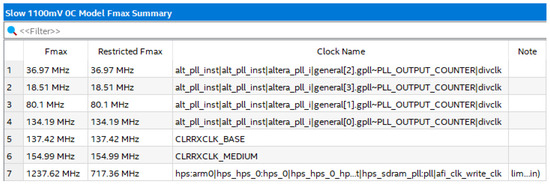
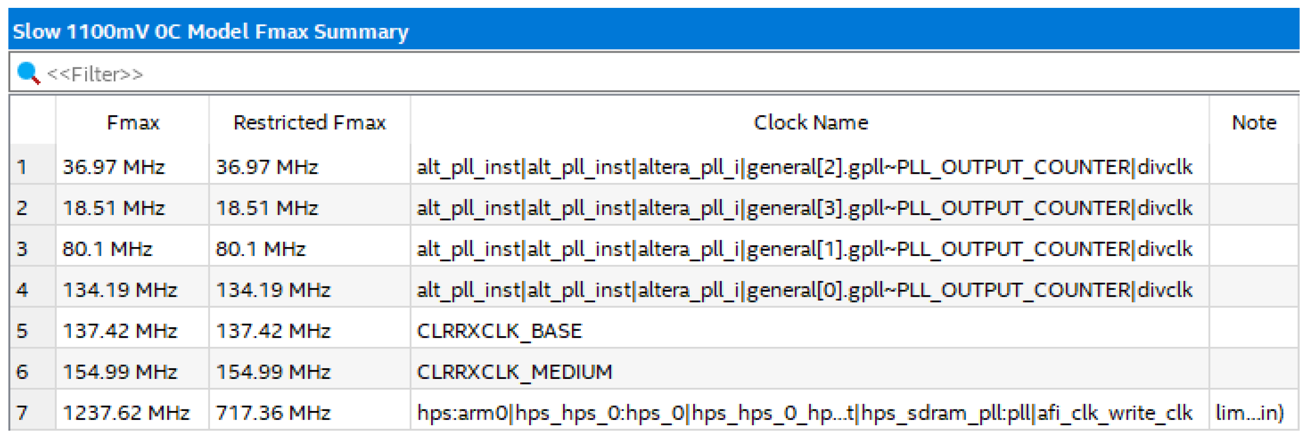
The timing analysis results presented in Figure 4 summarize the maximum achievable clock frequencies (Fmax) for the implemented design under slow 1100 mV conditions. The reported values confirm that all critical clock domains meet the specified timing constraints. In particular, the Camera Link receiver clock domain CLRRXCLK_BASE satisfies the required operating frequency of 82 MHz, as the achieved Fmax significantly exceeds this requirement. Additionally, the PLL-generated output clocks are correctly constrained and validated, with target frequencies of 100 MHz, 50 MHz, 25 MHz, and 5 MHz for PLL outputs 0, 1, 2, and 3, respectively. The analysis demonstrates sufficient timing margin across all domains, indicating reliable operation of the acquisition and processing pipeline under the defined system constraints.
Figure 4.
Fmax summary report after the post-place and route for the FPGA design under slow 1100 mV operating conditions, showing achieved maximum frequencies for the Camera Link receiver clocks and PLL-generated clocks.
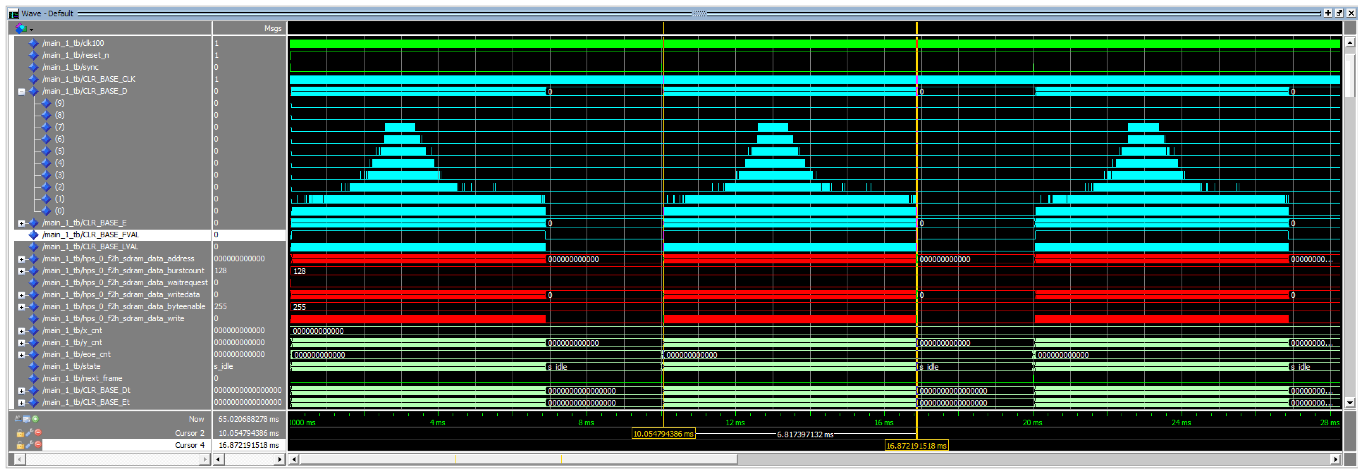
Figure 5 shows the ModelSim timing simulation of the Camera Link acquisition subsystem and the SDRAM memory controller. The cyan waveforms correspond to the Camera Link interface signals, while the red waveforms represent the SDRAM controller activity during frame storage. The simulation illustrates the acquisition of three consecutive image frames with a resolution of 1 Mpixel and a pixel depth of 10 bits under external synchronization at 100 Hz, corresponding to a 10 ms frame period.
Figure 5.
Timing simulation of the Camera Link acquisition pipeline and SDRAM frame storage for three consecutive 1-Mpixel frames.
The simulated camera model corresponds to the acA2000-340kc device, which transmits pixel data using an 82 MHz clock. The duration of frame transmission is indicated by the high level of the frame-valid signal CLR_BASE_FVAL. Two cursors mark the corresponding interval of approximately 6.82 ms, which represents the active period of pixel transmission. The line-valid signal CLR_BASE_LVAL indicates valid pixel intervals for individual image rows.
The waveform further shows that memory write operations performed by the SDRAM controller occur during the same interval, as indicated by the signal sdram_data_write. This confirms that the complete image frame is stored in external memory within the 6.82 ms acquisition period. Since the synchronization period is 10 ms, the implemented architecture satisfies real-time operation requirements. The Camera Link interface controller, frame synchronization logic, and SDRAM controller process the incoming pixel stream and transfer data between modules without timing violations. The stored frames can subsequently be accessed by the ARM processor and transmitted to the host computer for further processing.
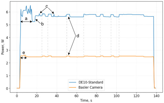
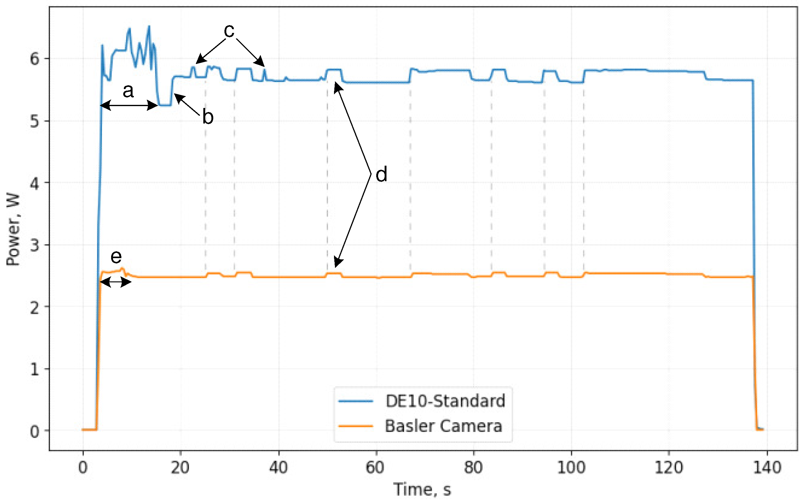
Figure 6 presents the measured power consumption profile of the FPGA-based frame-grabber system implemented on the DE10-Standard platform together with the connected Basler Camera Link camera. The measurement captures the dynamic behavior of the system across several operational phases, including system boot, application initialization, camera configuration, and active data acquisition. The results indicate that during continuous acquisition and streaming, the frame-grabber consumes approximately 5.8 W, while the camera requires about 2.5 W on average. The highest power consumption occurs during this phase, where synchronized peaks are observed in both modules due to intensive data transfer and real-time processing. In contrast, lower power levels are observed during initialization and configuration stages. These results demonstrate that the system maintains stable and predictable power characteristics, with peak consumption directly associated with high-throughput operation typical for real-time embedded vision systems.
Figure 6.
Measured power consumption of the DE10-Standard FPGA-based frame-grabber system with Basler Camera Link camera during different operational phases: (a) Linux system boot, (b) application start-up, (c) camera configuration, (d) synchronized peaks of increased power consumption in both the frame-grabber and camera during continuous image acquisition and data streaming to the host PC, and (e) camera initialization (boot).
Figure 7 presents representative image frames captured using the Basler acA2000-340kc industrial camera and acquired by the proposed FPGA-based frame-grabber system. The images were obtained through the Camera Link interface and stored in the external DDR memory using the low-latency acquisition pipeline implemented in the FPGA fabric. The presented samples demonstrate that the implemented acquisition architecture correctly reconstructs the incoming pixel stream and stores complete image frames without data loss or timing violations. The captured frames are subsequently accessed by the embedded ARM processor through the shared memory subsystem and transmitted to the host computer for visualization and further processing. These results confirm the correct operation of the entire acquisition chain, including the Camera Link receiver, frame formatting logic, SDRAM buffering, and AXI-based communication between the FPGA fabric and the ARM processor subsystem.
Figure 7.
Example image frames acquired by the FPGA-based Camera Link frame-grabber using the Basler acA2000-340kc industrial camera.
Table 8 situates the proposed architecture alongside representative FPGA- and SoC-oriented security studies from our reference set that implement overlapping protection mechanisms or report comparable implementation metrics. The comparison is necessarily interpretive because prior works target different devices (e.g., Xilinx LUT/FF/DSP reporting versus Intel ALM accounting), different threat models (on-chip communication hardening, attestation, side-channel monitoring, or NoC-centric encryption), and different application stacks; nevertheless, the collected results illustrate a consistent trade-off between protection breadth, fabric cost, and runtime impact. Lightweight authenticated schemes with explicit replay handling and CPU–FPGA secure data paths can achieve strong cryptographic properties but may consume thousands of slice LUTs and substantial BRAM or depend on software-side crypto latency that grows with payload size [25,32], whereas hardware integrity or runtime-attestation approaches report non-negligible processor CPI overhead or CLB utilization depending on the monitored program and attestation prototype [23,29]. ML-assisted tampering or intrusion frameworks and power-side-channel monitors can achieve very high detection rates but typically require larger or DSP-heavy accelerators and monitoring infrastructure that are not co-located with a gigabit-scale vision pixel pipe [20,26]. Against this backdrop, the results above show that integrating the full set of vision-oriented monitoring and optional ASCON protection requires only about 1.6% additional ALM utilization on the Cyclone V platform while preserving the measured 100 fps acquisition and ≈1.05 Gbps stream throughput, which highlights the practical advantage of the presented approach for real-time embedded vision on resource-constrained SoC FPGAs. Specialized designs such as high-performance PUF instantiations or secure NoC routers remain complementary references for device authentication and on-chip transport security rather than direct substitutes for an end-to-end Camera Link acquisition and streaming path [27,31].
Table 8.
Qualitative and quantitative comparison with representative works from our bibliography that report overlapping security mechanisms or publish FPGA/performance metrics. ALM: Adaptive Logic Module (Intel). LUT/FF: Xilinx-style combinational/sequential fabric.
4.4. Limitations
Despite the successful implementation and evaluation of the proposed FPGA-based security architecture, several limitations should be acknowledged. First, the presented security modules focus primarily on lightweight hardware mechanisms designed to protect the data acquisition pipeline and control communication with minimal resource overhead. As a result, the implemented security primitives do not provide a complete cryptographic security framework comparable to full hardware security modules used in high-assurance systems. Instead, the architecture prioritizes low latency and small logic utilization suitable for real-time embedded vision applications.
Second, while the presented evaluation focuses on runtime data-path and control-path attacks relevant to embedded vision pipelines, advanced threats such as side-channel analysis and hardware Trojans are considered out of scope. These represent complementary security layers that can be integrated with the proposed architecture in future work.
Another limitation concerns the scale of the experimental setup. The implemented prototype uses a single camera connected through a Camera Link interface and operates within a controlled laboratory environment. In larger distributed vision systems with multiple sensors, network nodes, and remote control interfaces, additional security mechanisms such as secure key distribution, remote attestation, and device lifecycle management would be necessary.
The current work focuses on the FPGA layer of the system architecture. Although a secure communication interface with the embedded ARM processor is implemented, the software security of the operating system, network stack, and host-side applications is outside the scope of this study. Future work could therefore explore the integration of hardware and software security mechanisms to provide a comprehensive end-to-end protection framework for embedded vision systems.
5. Conclusions
This paper presented a hardware-assisted security architecture for FPGA-ARM embedded vision systems operating in network-connected environments. The proposed solution integrates multiple lightweight hardware security modules directly into the image acquisition and communication pipeline of a Cyclone V SoC-based frame-grabber system. The implemented architecture combines frame replay detection, CRC-based data integrity verification, frame sequence monitoring, authenticated command execution, communication anomaly monitoring, and hardware-rooted trust primitives, including a ring oscillator PUF and pseudo-random number generator. An optional ASCON-based authenticated encryption core further enables secure data communication between the embedded vision node and the host system.
Experimental evaluation using a Camera Link industrial camera demonstrated that the complete security architecture introduces only about 1.6% additional FPGA logic utilization while preserving real-time system performance at data rates exceeding 1 Gbps. The results confirm that hardware-assisted protection mechanisms can effectively improve the resilience of embedded vision platforms against data manipulation, replay attacks, and unauthorized control attempts without compromising acquisition throughput. The lightweight, pipeline-integrated security mechanisms can provide measurable protection against practical attack scenarios while preserving deterministic high-throughput operation, bridging the gap between theoretical security models and deployable embedded vision systems.
Future work will focus on extending the architecture with advanced cryptographic protocols, remote attestation mechanisms, and tighter integration of hardware and software security layers in order to provide a comprehensive end-to-end protection framework for distributed embedded vision systems and industrial edge computing platforms.
Author Contributions
Conceptualization, T.S. and D.A.; methodology, D.A.; software, T.S.; validation, T.S.; formal analysis, D.A.; investigation and analysis, T.S.; data curation, D.A.; writing—original draft preparation, T.S. and D.A.; writing—review and editing, T.S. and D.A.; visualization, T.S. and D.A. All authors have read and agreed to the published version of the manuscript.
Funding
The publication was co-funded by the European Union under the Horizon Europe program, grant agreement No. 101059903, by the European Union funds for the period 2021–2027, and by the state budget of the Republic of Lithuania, financial agreement No. 10-042-P-0001.
Data Availability Statement
The original code and data presented in this study will be made available by the authors on request.
Conflicts of Interest
The authors declare no conflicts of interest.
References
- Meribout, M.; Baobaid, A.; Khaoua, M.O.; Tiwari, V.K.; Pena, J.P. State of art IoT and Edge embedded systems for real-time machine vision applications. IEEE Access 2022, 10, 58287–58301. [Google Scholar] [CrossRef] [Scilit]
- Biglari, A.; Tang, W. A review of embedded machine learning based on hardware, application, and sensing scheme. Sensors 2023, 23, 2131. [Google Scholar] [CrossRef] [Scilit]
- Zhou, Z.; Duan, X.; Han, J. A design framework for generating energy-efficient accelerator on FPGA toward low-level vision. IEEE Trans. Very Large Scale Integr. (VLSI) Syst. 2024, 32, 1485–1497. [Google Scholar] [CrossRef] [Scilit]
- Castells-Rufas, D.; Ngo, V.; Borrego-Carazo, J.; Codina, M.; Sanchez, C.; Gil, D.; Carrabina, J. A survey of FPGA-based vision systems for autonomous cars. IEEE Access 2022, 10, 132525–132563. [Google Scholar] [CrossRef] [Scilit]
- Chowdhury, M.R.Z.; Seum, A.; Talukder, M.R.; Amin, R.A.; Hossain, F.S.; Obermaisser, R. Towards Next-Generation FPGA-Accelerated Vision-Based Autonomous Driving: A Comprehensive Review. Signals 2025, 6, 53. [Google Scholar] [CrossRef] [Scilit]
- Al Amin, R.; Hasan, M.; Wiese, V.; Obermaisser, R. FPGA-based real-time object detection and classification system using YOLO for edge computing. IEEE Access 2024, 12, 73268–73278. [Google Scholar] [CrossRef] [Scilit]
- Al-Shamma, O.; Fadhel, M.A. Trusted outdoor multi-camera tracking system powered by FPGA. J. Eng. Res. 2024, 13, 3092–3106. [Google Scholar] [CrossRef] [Scilit]
- Monjur, M.M.R.; Heacock, J.; Calzadillas, J.; Mahmud, M.S.; Roth, J.; Mankodiya, K.; Sazonov, E.; Yu, Q. Hardware security in sensor and its networks. Front. Sens. 2022, 3, 850056. [Google Scholar] [CrossRef] [Scilit]
- Zhang, J.; Qu, G. Recent attacks and defenses on FPGA-based systems. ACM Trans. Reconfigurable Technol. Syst. (TRETS) 2019, 12, 1–24. [Google Scholar] [CrossRef] [Scilit]
- Moraitis, M. FPGA bitstream modification: Attacks and countermeasures. IEEE Access 2023, 11, 127931–127955. [Google Scholar] [CrossRef] [Scilit]
- Alsuwaiyan, A.; Habib, A.A.; Imoukhuede, A.B.; Omar, M.O.; Maruf, M.A.; Alqarni, M.; El-Maleh, A.; Tabbakh, A.; Felemban, M.; Azim, A. A systematic literature review on vulnerabilities, mitigation techniques, and attacks in field-programmable gate arrays. Arab. J. Sci. Eng. 2025, 50, 611–641. [Google Scholar] [CrossRef] [Scilit]
- Proulx, A.; Chouinard, J.Y.; Fortier, P.; Miled, A. A survey on FPGA cybersecurity design strategies. ACM Trans. Reconfig. Technol. Syst. 2023, 16, 1–33. [Google Scholar] [CrossRef] [Scilit]
- Muttaki, M.R.; Rahman, M.H.; Kulkarni, A.; Tehranipoor, M.; Farahmandi, F. Ftc: A universal framework for fault-injection attack detection and prevention. IEEE Trans. Very Large Scale Integr. (VLSI) Syst. 2024, 32, 1311–1324. [Google Scholar] [CrossRef] [Scilit]
- Hayashi, S.; Sakamoto, J.; Matsumoto, T. Design methodology of digital sensors for detecting laser fault injection attacks in FPGAs: S. Hayashi et al. J. Cryptogr. Eng. 2025, 15, 12. [Google Scholar] [CrossRef] [Scilit]
- Sriraman, H. Decoding the Solution for Man-at-the-End Attacks and Reverse Engineering on IoMT Devices: An Experimental Review of Techniques and Defences. J. Multidiscip. Healthc. 2025, 18, 6479. [Google Scholar]
- Kawser Ahmed, M.; Panoff Kealoha, M.; Mandebi Mbongue, J.; Saha, S.K.; Nghonda Tchinda, E.; Mbua, P.E.; Bobda, C. Multi-Tenant Cloud FPGA: A Survey on Security, Trust, and Privacy. ACM Trans. Reconfigurable Technol. Syst. 2025, 18, 1–44. [Google Scholar] [CrossRef] [Scilit]
- Mehta, A. Multi-Tenant Cloud Architectures Utilizing FPGAs: Security Challenges, Design Methodologies, and Proposed Paradigms. Stanf. Database Libr. Am. J. Appl. Sci. Technol. 2025, 5, 303–308. [Google Scholar]
- Chatterjee, D.; Maitra, S.; Mishra, N.; Shukla, S.; Mukhopadhyay, D. Hardware security in the connected world. Wiley Interdiscip. Rev. Data Min. Knowl. Discov. 2025, 15, e70034. [Google Scholar] [CrossRef] [Scilit]
- Akter, S.; Khalil, K.; Bayoumi, M. A survey on hardware security: Current trends and challenges. IEEE Access 2023, 11, 77543–77565. [Google Scholar] [CrossRef] [Scilit]
- Wang, H.; Halak, B. TampML: Tampering attack detection and malicious nodes localization in NoC-based MPSoC. IEEE Trans. Emerg. Top. Comput. 2024, 13, 551–562. [Google Scholar] [CrossRef] [Scilit]
- Williams, B.; Awad, R.A.; Mulkey, C.; Ciocarlie, G.; Ismail, M.; Saleeby, K. Securing Smart Manufacturing: Detection of Cyber–physical Attacks in CNC-Based Systems. In Proceedings of the 2025 IEEE International Symposium on Hardware Oriented Security and Trust (HOST); IEEE: New York, NY, USA, 2025; pp. 428–438. [Google Scholar]
- Hanif, U.; Aman, M.N.; Sikdar, B. Alexis: Anomaly-Based Intrusion Detection in FPGA-Enabled Cyber–physical Systems. IEEE Trans. Ind. Cyber-Phys. Syst. 2025, 4, 106–118. [Google Scholar] [CrossRef] [Scilit]
- Hao, Q.; Zhang, Z.; Xu, D.; Wang, J.; Liu, J.; Zhang, J.; Ma, J.; Wang, X. A hardware security-monitoring architecture based on data integrity and control flow integrity for embedded systems. Appl. Sci. 2022, 12, 7750. [Google Scholar] [CrossRef] [Scilit]
- Latif, S.; Djenouri, D.; Idrees, Z.; Ahmad, J.; Zou, Z. Hardware security modules for secure communications in the Industrial Internet of Things. IEEE Commun. Surv. Tutor. 2025, 28, 64–108. [Google Scholar] [CrossRef] [Scilit]
- Chen, T.; Tan, Y.A.; Li, C.; Zhang, Z.; Meng, W.; Li, Y. Securecomm: A secure data transfer framework for neural network inference on CPU-FPGA heterogeneous edge devices. IEEE J. Emerg. Sel. Top. Circuits Syst. 2024, 14, 811–822. [Google Scholar] [CrossRef] [Scilit]
- Zhang, T.; Tehranipoor, M.; Farahmandi, F. Trustguard: Standalone FPGA-based security monitoring through power side-channel. IEEE Trans. Very Large Scale Integr. (VLSI) Syst. 2023, 32, 319–332. [Google Scholar] [CrossRef] [Scilit]
- Anandakumar, N.N.; Hashmi, M.S.; Sanadhya, S.K. Design and analysis of FPGA-based PUFs with enhanced performance for hardware-oriented security. ACM J. Emerg. Technol. Comput. Syst. (JETC) 2022, 18, 1–26. [Google Scholar] [CrossRef] [Scilit]
- Oyama, T.; Hagizaki, M.; Okura, S.; Fujino, T. Implementation of an image tampering detection system with a CMOS image sensor PUF and OP-TEE. Sensors 2024, 24, 7121. [Google Scholar] [CrossRef] [Scilit]
- Usama, M.; Aman, M.N.; Sikdar, B. Runtime self-attestation of FPGA-based IoT devices. IEEE Internet Things J. 2024, 11, 33406–33417. [Google Scholar] [CrossRef] [Scilit]
- Wang, Y.; Chang, X.; Zhu, H.; Wang, J.; Gong, Y.; Li, L. Towards secure runtime customizable trusted execution environment on FPGA-SoC. IEEE Trans. Comput. 2024, 73, 1138–1151. [Google Scholar] [CrossRef] [Scilit]
- Nagalaxmi, T.; Rao, E.S.; ChandraSekhar, P. FPGA-based implementation and verification of hybrid security algorithm for NoC architecture. Analog. Integr. Circuits Signal Process. 2024, 121, 13–23. [Google Scholar] [CrossRef] [Scilit]
- Gladis Kurian, M.; Chen, Y. Ascon on FPGA: Post-quantum safe authenticated encryption with replay protection for IoT. Electronics 2025, 14, 2668. [Google Scholar] [CrossRef] [Scilit]
- Sureshkumar, V.; Chinnaraj, P.; Saravanan, P.; Amin, R.; Rodrigues, J.J. Authenticated key agreement protocol for secure communication establishment in vehicle-to-grid environment with FPGA implementation. IEEE Trans. Veh. Technol. 2022, 71, 3470–3479. [Google Scholar] [CrossRef] [Scilit]
- Roy, K.S.; Sujith, M.; Bhanu, B.; Preethi; Hazarika, R.A. FPGA-based dual-layer authentication scheme utilizing AES and ECC for unmanned aerial vehicles. EURASIP J. Wirel. Commun. Netw. 2024, 2024, 91. [Google Scholar] [CrossRef] [Scilit]
- Alqarni, M.; Azim, A. SecureLLAMA: Secure FPGAs using LLAMA large language models. IEEE Trans. Artif. Intell. 2025, 6, 2266–2280. [Google Scholar] [CrossRef] [Scilit]



Disclaimer/Publisher’s Note: The statements, opinions and data contained in all publications are solely those of the individual author(s) and contributor(s) and not of MDPI and/or the editor(s). MDPI and/or the editor(s) disclaim responsibility for any injury to people or property resulting from any ideas, methods, instructions or products referred to in the content. |
© 2026 by the authors. Licensee MDPI, Basel, Switzerland. This article is an open access article distributed under the terms and conditions of the Creative Commons Attribution (CC BY) license.