1. Introduction
Defected ground structures (DGS) have been widely employed in microwave planar devices due to their ability to effectively modify the propagation characteristics of transmission lines. By etching specific patterns in the ground-plane, a DGS perturbs the surface current distribution, introducing additional effective inductance and capacitance into the structure. This mechanism leads to slow-wave propagation, improved impedance characteristics, and enhanced suppression of undesired harmonics [
1].
Owing to these properties, DGS has been extensively utilized in the development of compact and high-performance microwave components, particularly in filter design [
2,
3,
4,
5,
6]. In low-pass filters (LPFs), the incorporation of DGS enables sharper roll-off characteristics and improved stopband attenuation without increasing the filter order. This approach enhances filter performance while maintaining structural simplicity and reduced circuit complexity.
Conventional LPF designs often require higher-order configurations to achieve a wide stopband, which results in increased circuit size and implementation complexity. In contrast, DGS-based filters provide an effective alternative by enhancing the equivalent inductive–capacitive response through ground-plane modification, thereby improving frequency selectivity and harmonic suppression. However, achieving a wide stopband with high attenuation while maintaining compact dimensions remains a challenging task.
In this work, a quasi-eight-shaped defected ground structure is proposed for the design of a compact low-pass filter. The proposed geometry modifies the ground current path, generating enhanced inductive and capacitive effects that enable effective control of the cutoff frequency through geometrical parameter adjustment. Compared with conventional LPFs, the proposed structure achieves sharp transition characteristics and a wide stopband while preserving a simple planar configuration.
The filter is implemented on an FR4 substrate with a thickness of 1.6 mm and a relative permittivity of 3.38, ensuring low-cost fabrication and compatibility with standard printed circuit board (PCB) technology.
The main contributions of this work can be summarized as follows. A novel figure-eight-shaped defected ground structure (DGS) is proposed for low-pass filter applications. The introduced geometry effectively modifies the ground current distribution, thereby producing additional inductive and capacitive effects. Based on this structure, a compact low-pass filter operating at 2.1 GHz is designed and experimentally validated, with an insertion loss lower than 1 dB in the passband and a wide stopband extending from 2.8 GHz to 8.5 GHz, with attenuation exceeding 26 dB. An equivalent circuit model is developed to provide physical insight into the filtering mechanism and to clarify the relationship between the DGS geometrical parameters and the electromagnetic response. Furthermore, a parametric analysis demonstrates controllable frequency behavior through geometrical modification. The proposed filter occupies a compact size of 20 mm × 50 mm (approximately 0.14λ0 × 0.35λ0 at 2.1 GHz), making it suitable for integration into microwave front-end and antenna systems.
2. Structure of the Proposed Quasi-Eight DGS
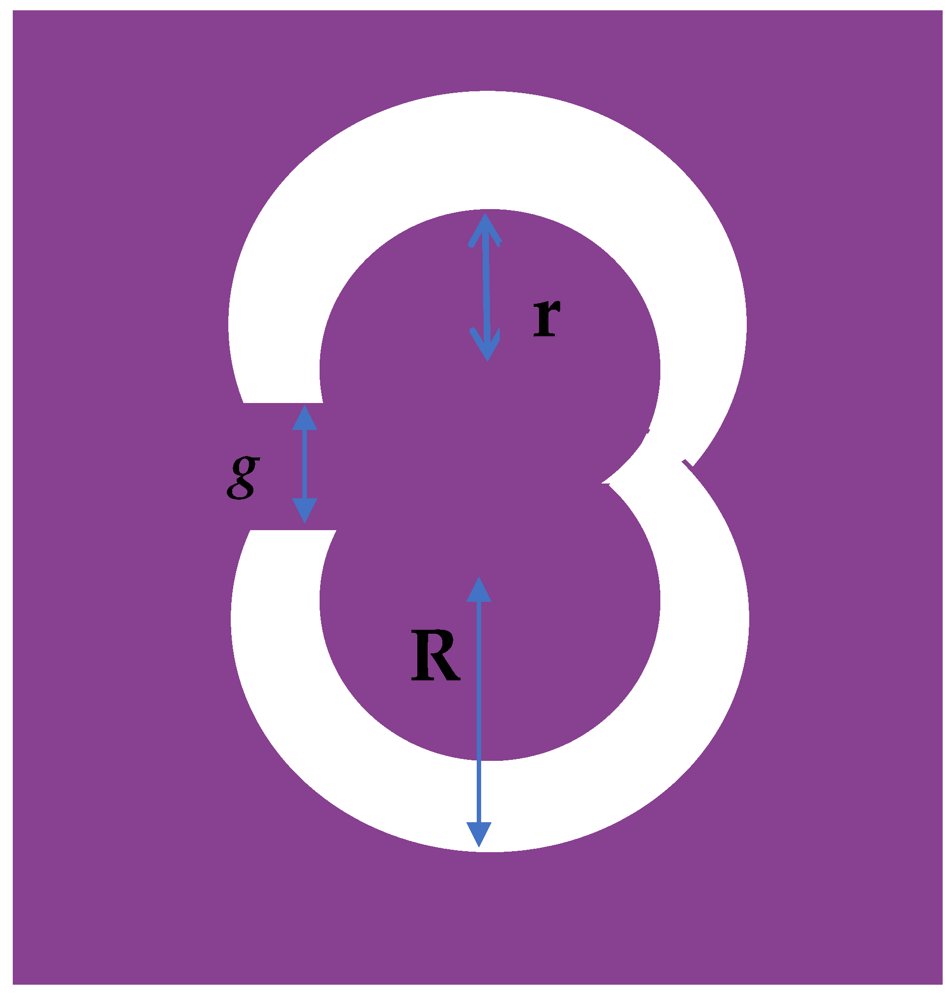
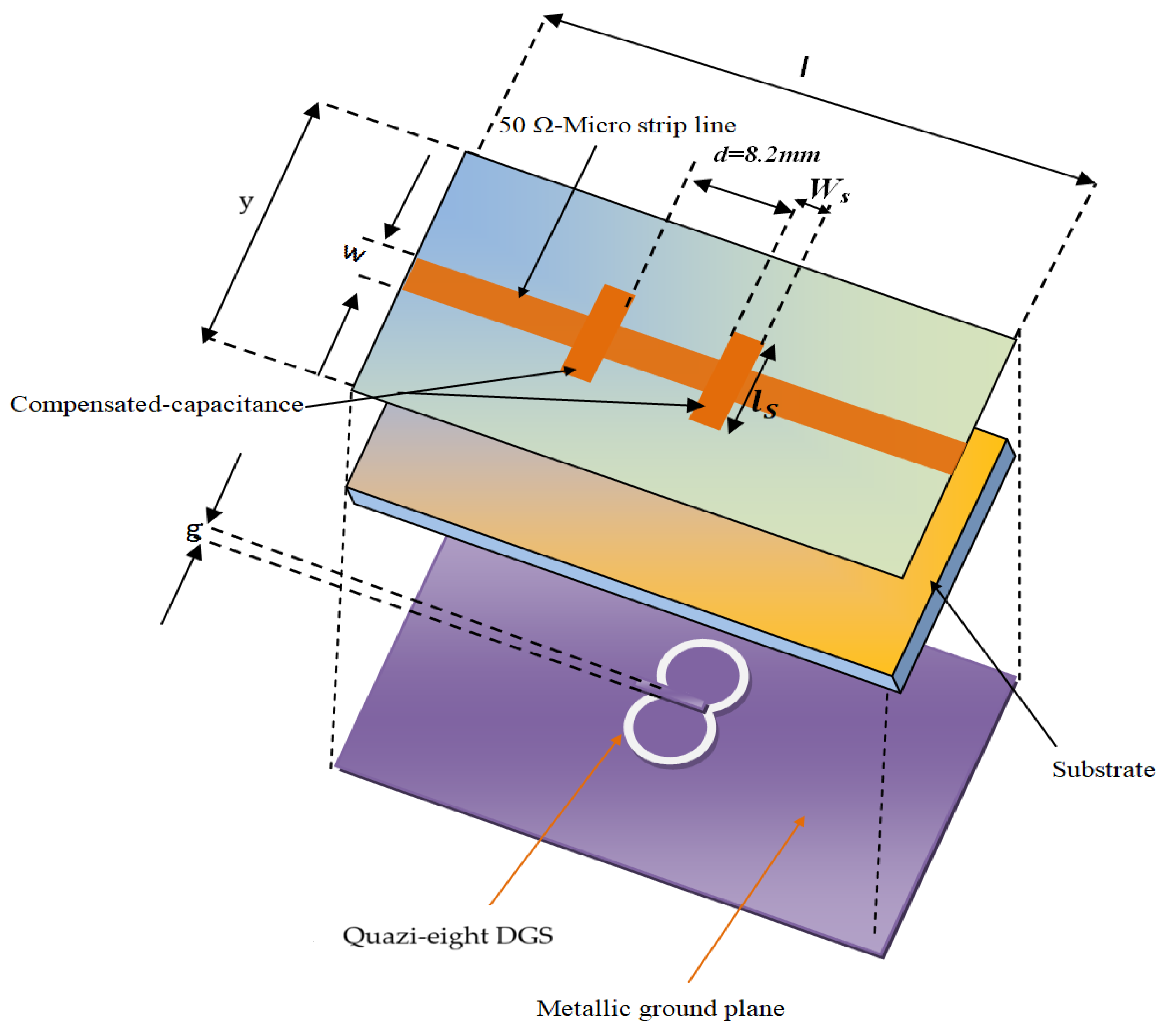
The geometry of the proposed quasi-eight defected ground structure (DGS) is illustrated in
Figure 1. The structure consists of two intersecting circular slots etched on the ground-plane, forming a quasi-eight configuration. The radii of the outer and inner circular sections are denoted by R and r, respectively, while the gap g varies from 1 mm to 3 mm. An FR4 dielectric substrate with a relative permittivity of
= 3.38 and a thickness of
h = 1.6 mm is used. The optimized geometrical parameters are summarized in
Table 1. The proposed geometry modifies the ground-plane current distribution, resulting in enhanced effective inductance and capacitance that contribute to the desired resonant behavior. Compared with conventional DGS geometries, such as the H-shaped DGS [
7], the proposed quasi-eight structure provides a more compact layout while maintaining effective current perturbation and strong resonant characteristics.
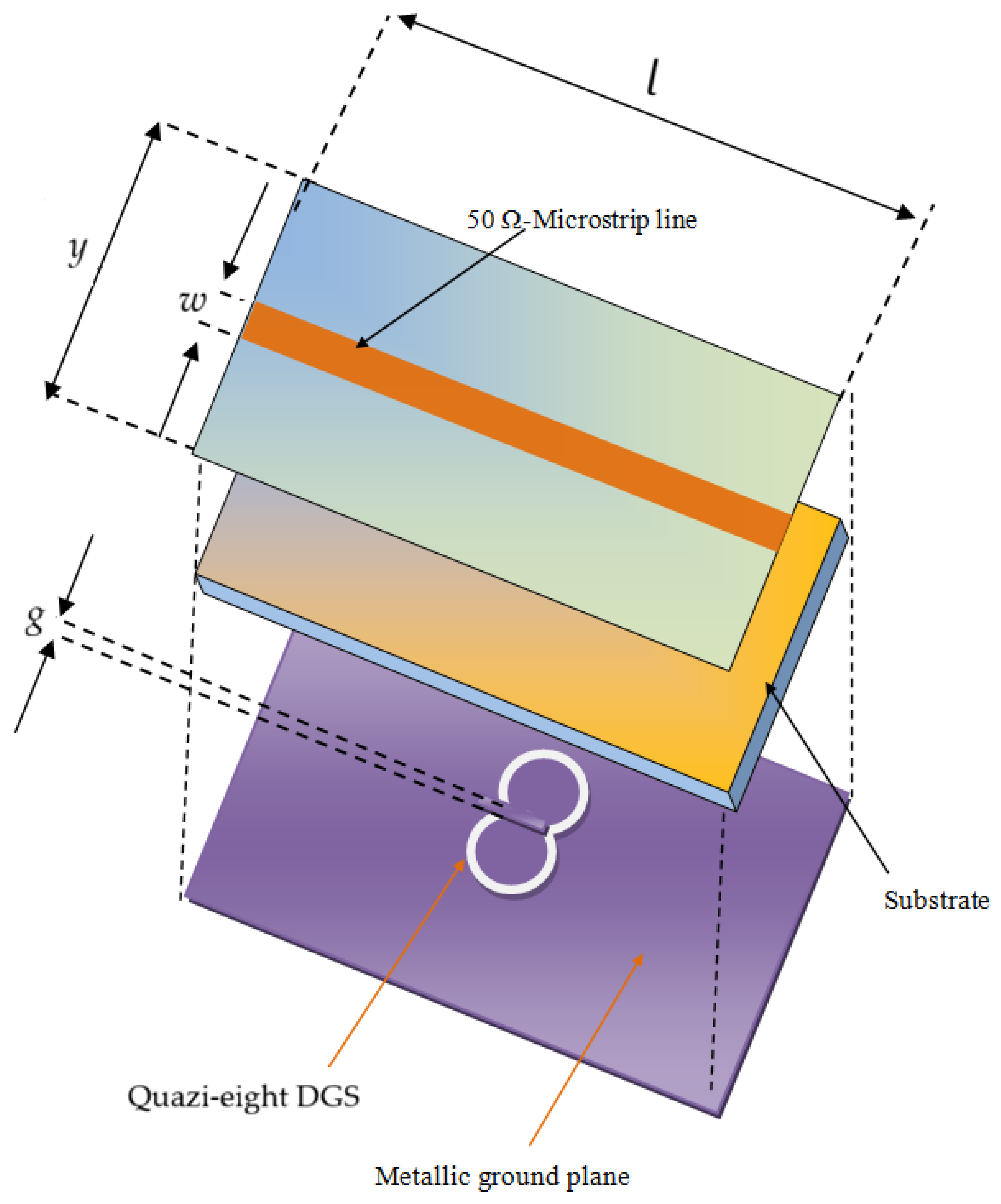
The complete geometry of the proposed filter is illustrated in
Figure 2, while the optimized dimensional parameters are listed in
Table 1.
The introduction of the quasi-eight DGS in the ground-plane produces additional effective inductance and capacitance due to the perturbation of the current distribution [
8,
9,
10,
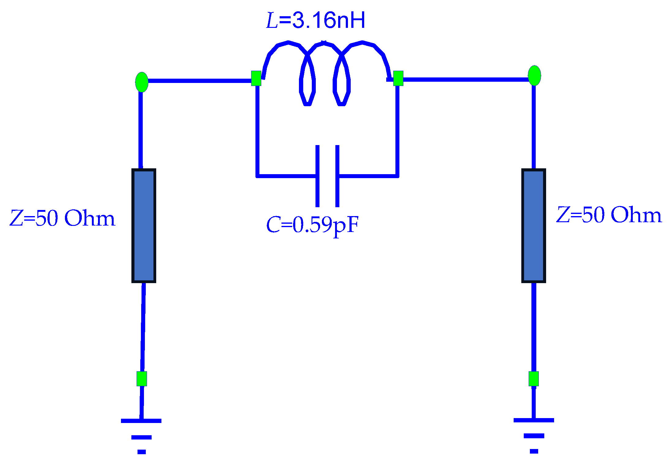
11]. This behavior can be modeled using a parallel
LC resonant circuit, as illustrated in
Figure 3.
The equivalent capacitance
and inductance
can be extracted from the cutoff frequency
and the resonant frequency
using the following expressions:
where
represents the cutoff frequency,
denotes the resonant frequency, and
is the characteristic impedance of the transmission line (typically 50 Ω).
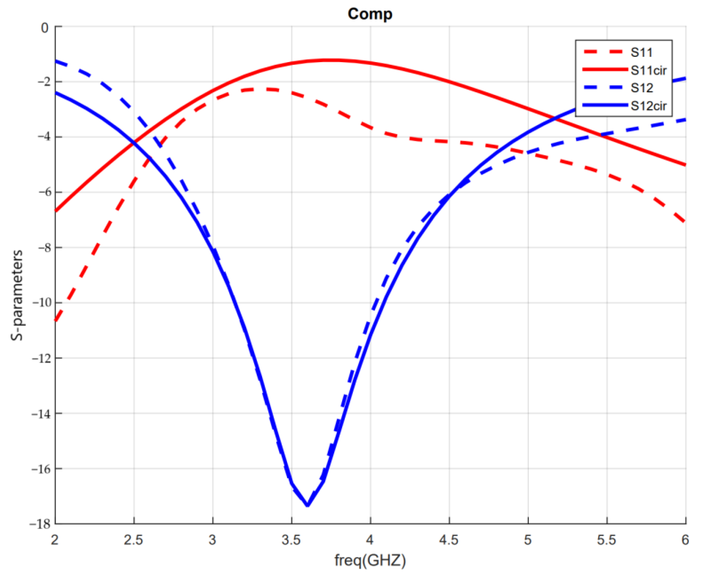
Figure 4 compares the full-wave electromagnetic response of the single DGS (dashed curves) with that predicted by the proposed equivalent circuit model (solid curves).
From
Figure 4, good agreement between the two responses can be observed in the vicinity of the fundamental resonance. The equivalent circuit accurately predicts the notch behavior around 3.6 GHz, where the minimum transmission coefficient |S
21| is approximately −17 dB in both the full-wave electromagnetic (EM) simulation and the circuit model. Minor discrepancies between the two responses are mainly attributed to distributed transmission-line effects, fringing fields, and parasitic coupling mechanisms, which are inherently included in the EM simulation but cannot be fully represented by the simplified lumped-element model. As commonly reported in previous DGS modeling studies and microwave filter theory [
1], lumped-element equivalent circuits effectively capture the dominant resonant behavior; however, slight deviations may arise at higher frequencies where distributed effects become significant. Overall, the close correspondence near the resonance frequency indicates that the dominant filtering mechanism originates from the resonant interaction between the effective inductance and capacitance introduced by the DGS geometry. This interaction perturbs the ground-plane current distribution and produces the notch characteristic, thereby confirming the validity of the proposed equivalent circuit model in describing the resonant behavior of the quasi-eight DGS.
3. Influence of the DGS Gap on the S Parameters
At this stage, all structural dimensions were fixed except for the DGS gap
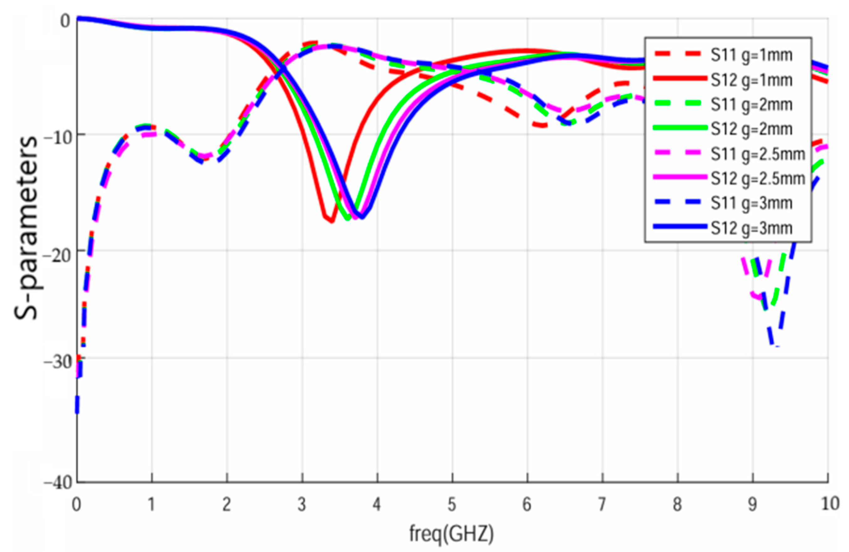
g, which was systematically varied to evaluate its effect on the filter response. The resulting S-parameter responses, illustrated in
Figure 5, clearly demonstrate the sensitivity of the cutoff frequency and stopband characteristics to variations in the gap parameter.
Figure 5 illustrates the variation in the S-parameters as the DGS gap g is varied. It can be observed that both the passband bandwidth and the resonant frequency increase with increasing gap width. This behavior is attributed to the reduction in the effective capacitance associated with the DGS when the gap becomes larger.
In contrast, smaller gap values (particularly for g < 1 mm) enhance the capacitive coupling between the defected regions, resulting in improved selectivity and a sharper transition between the passband and stopband.
The detailed numerical results corresponding to different gap values are summarized in
Table 2.
The results summarized in
Table 2 indicate that the cutoff frequency
, the resonant frequency
, and the stopband bandwidth BW increase as the gap dimension g becomes larger. This trend is consistent with the reduction in the effective capacitance associated with the DGS as the gap becomes wider. Moreover, the maximum transmission coefficient ∣
S21∣max slightly decreases with increasing gap width, reflecting a modification in the coupling strength within the structure. These observations confirm that precise frequency positioning can be achieved through structural parameter optimization without increasing circuit complexity. Therefore, the DGS gap serves as an effective tuning parameter for controlling the resonant characteristics of the proposed filter.
4. Design and Modeling of the Stub-Loaded Quasi-Eight DGS LPF
The modified DGS-based low-pass filter incorporates two open-circuited stubs, as illustrated in
Figure 6. The inclusion of these stubs introduces additional capacitive loading to the structure, thereby enhancing the overall coupling effect between the microstrip line and the defected ground region.
From the perspective of the equivalent circuit, the open-circuited stubs contribute to the parallel capacitance
, as expressed in Equation (3) [
8,
12]:
where
denotes the guided wavelength,
represents the characteristic impedance of the stub, and
is the physical length of the stub.
According to Equation (3), the capacitance increases with the stub length , which directly affects the total effective capacitance of the filter structure. Consequently, the addition of the two stubs modifies the resonant condition of the DGS-LPF and enhances both the selectivity and stopband performance.
The integration of stub loading with the quasi-eight DGS geometry therefore provides an effective approach for improving the filtering performance without increasing the filter order or structural complexity.
The elements
L,
C of
Figure 7 are extracted via Equations (1) and (2).
Figure 8 compares the full-wave electromagnetic (EM) response with that predicted by the developed equivalent circuit model.
From
Figure 8, it can be clearly seen that the developed model accurately predicts the passband characteristics and the cutoff frequency of the proposed structure. The slight deviation in the deep stopband region is mainly attributed to distributed transmission-line effects, parasitic coupling mechanisms, and higher-order electromagnetic phenomena that are inherently included in the full-wave simulation but cannot be fully represented by the simplified lumped-element model.
5. Design, Realization and Modeling of the Coupled QUASI-EIGHT DGS-LPF
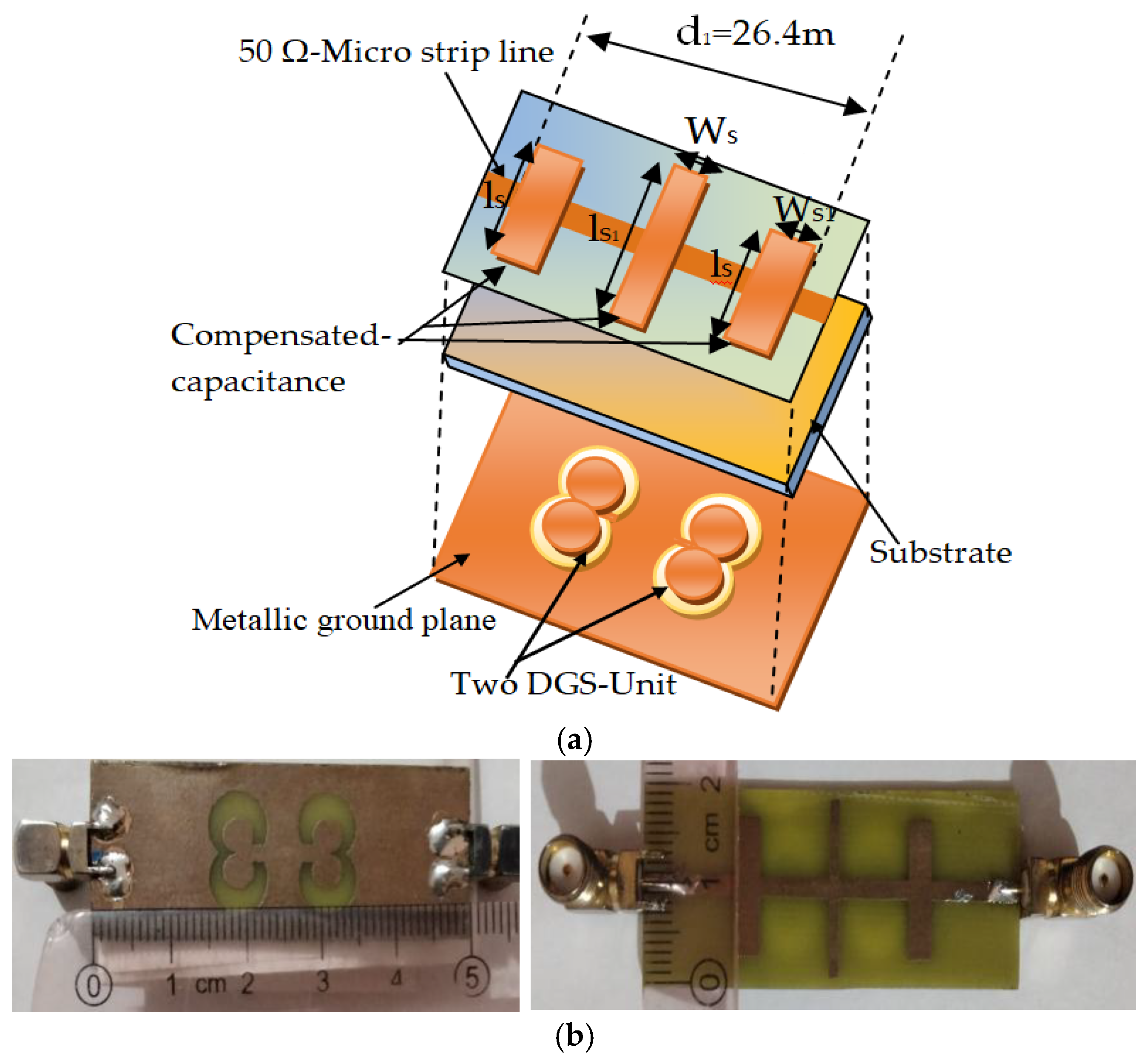
The proposed coupled quasi-eight DGS low-pass filter, depicted in
Figure 9a, incorporates flat-edge modifications into the DGS geometry to enhance electromagnetic coupling and field distribution. The fabricated prototype is shown in
Figure 9b. This structural refinement leads to improved filtering characteristics, including enhanced stopband suppression and more stable microwave-frequency performance, without increasing the overall circuit complexity.
The physical dimensions of the three stubs are summarized in
Table 3, whereas the geometrical parameters of the DGS are intentionally kept unchanged to isolate and evaluate the impact of the proposed modification.
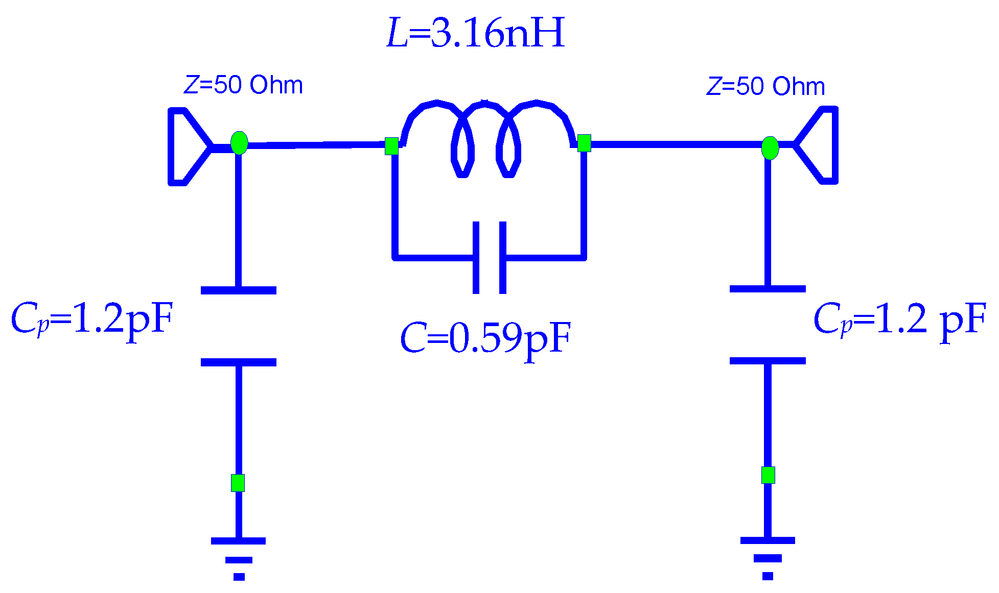
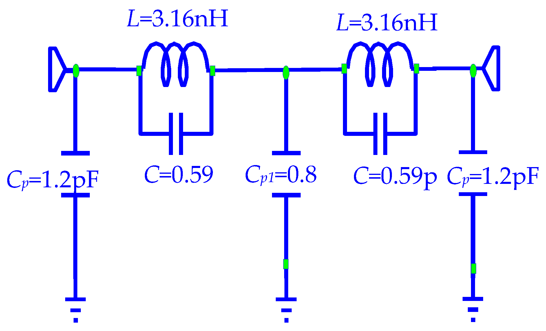
The equivalent circuit model is depicted in
Figure 10. The extracted lumped-element parameters are as follows:
and
, while the parasitic capacitances are
and
. The capacitance
is determined according to Equation (3).
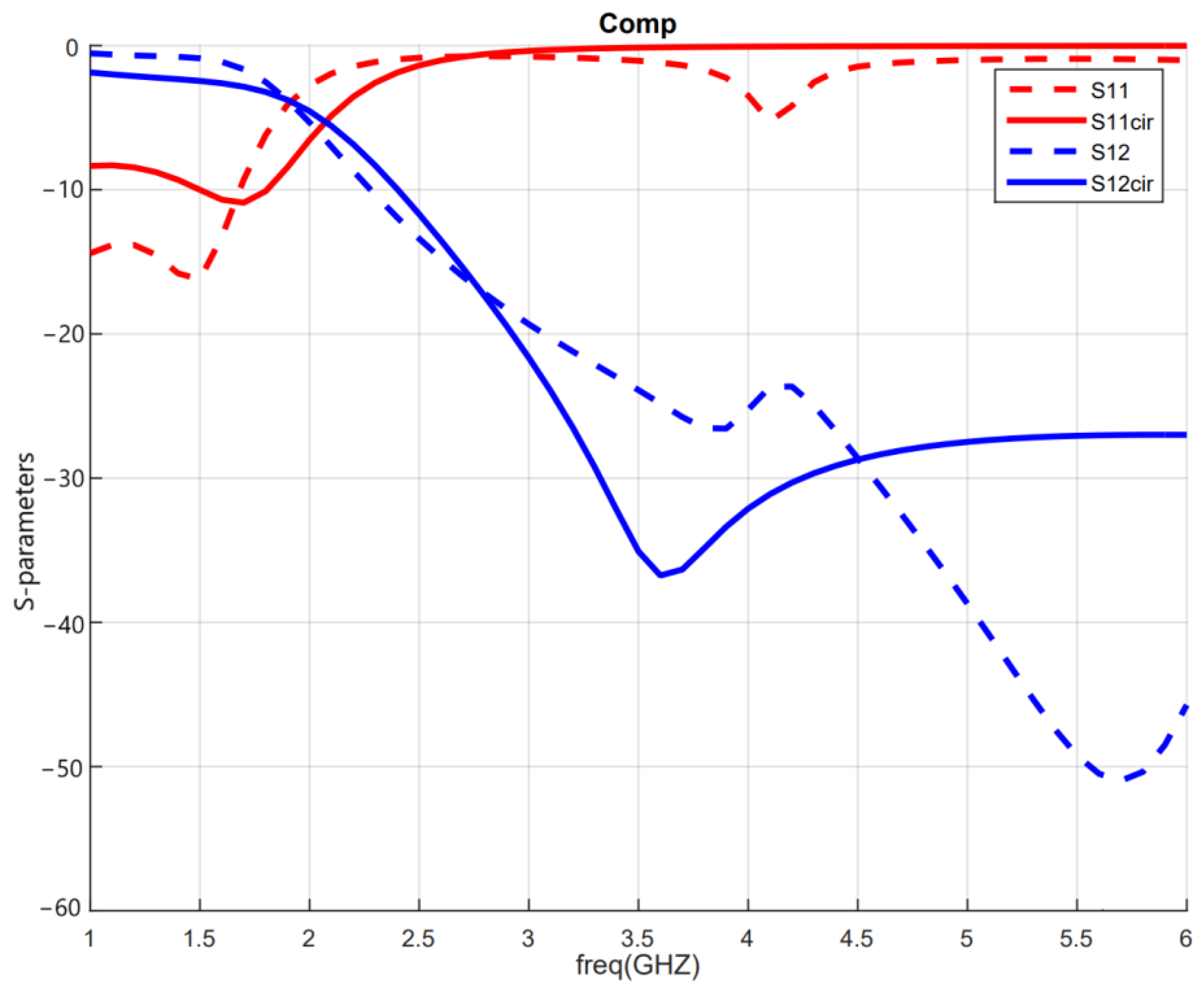
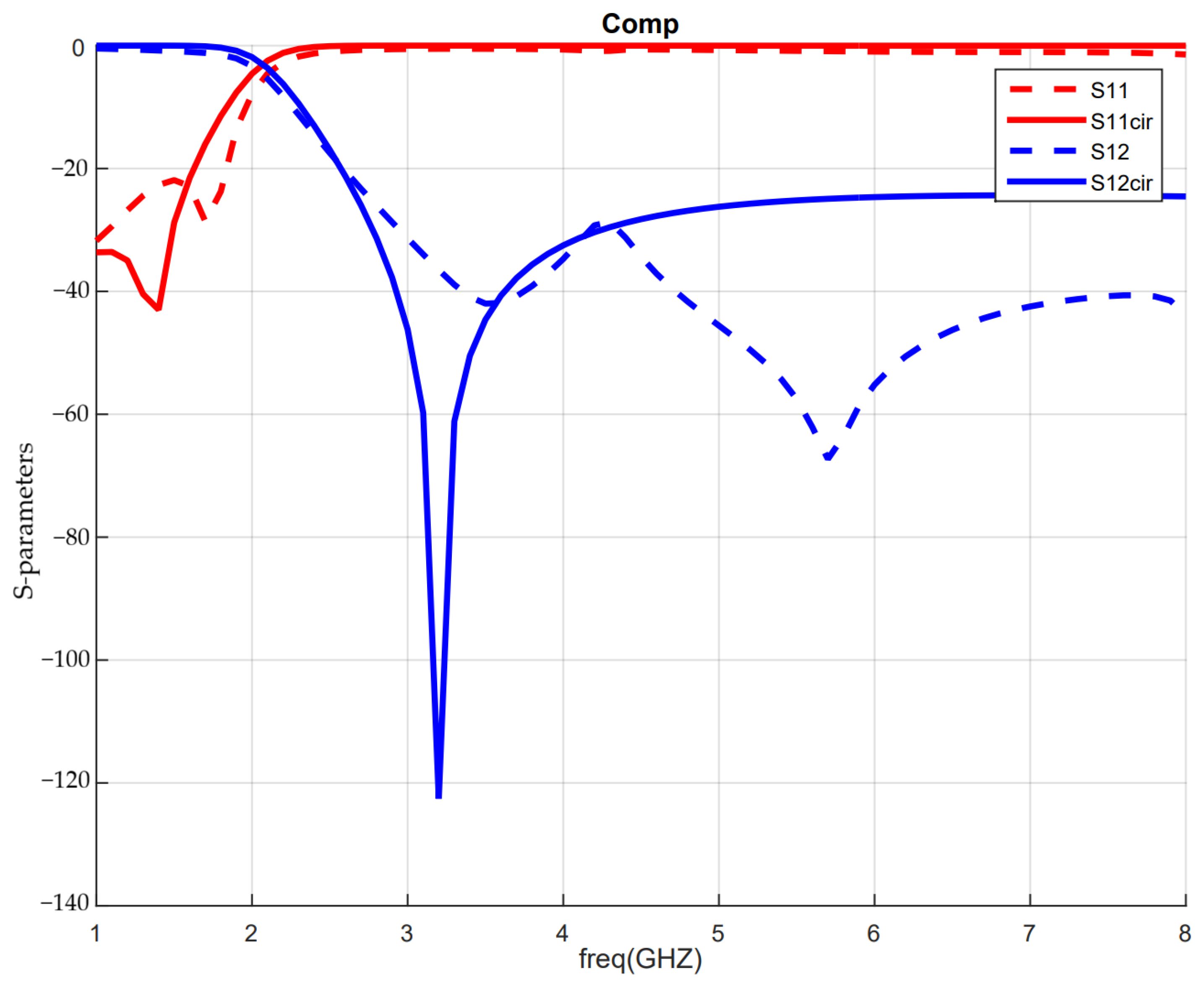
Figure 11 presents a comparison between the full-wave electromagnetic simulation and the developed equivalent circuit model for the proposed double-DGS low-pass filter.
Figure 11 shows good agreement in the passband and around the cutoff frequency, validating the accuracy of the extracted lumped-element parameters. Slight discrepancies appear near the attenuation pole and at higher frequencies due to the simplified lumped-element representation, which cannot fully capture the distributed electromagnetic coupling and parasitic effects inherently included in the full-wave EM simulation. Furthermore, the incorporation of two identical DGS units results in a higher-order filtering response, significantly improving the stopband performance. The rejection bandwidth extends up to approximately 6 GHz for a −20 dB attenuation level, confirming the effectiveness of the proposed configuration in enhancing stopband suppression.
6. Measurement and Performance Comparison
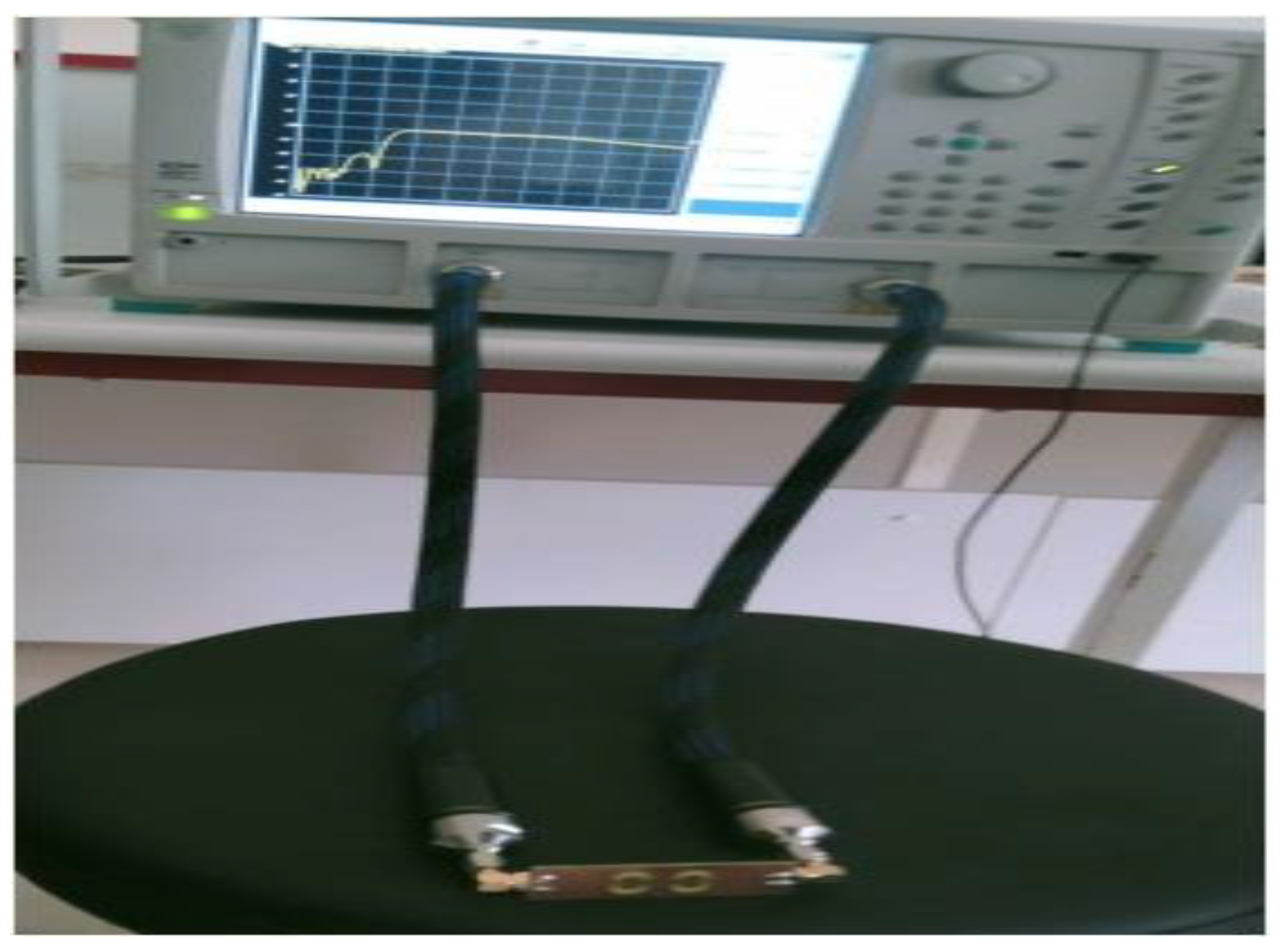
To experimentally validate the performance of the proposed DGS low-pass filter (LPF), measurements were carried out using a calibrated vector network analyzer (MS4644B VNA, Anritsu, Atsugi, Japan). The fabricated prototype was connected through SMA connectors after applying a standard SOLT calibration.
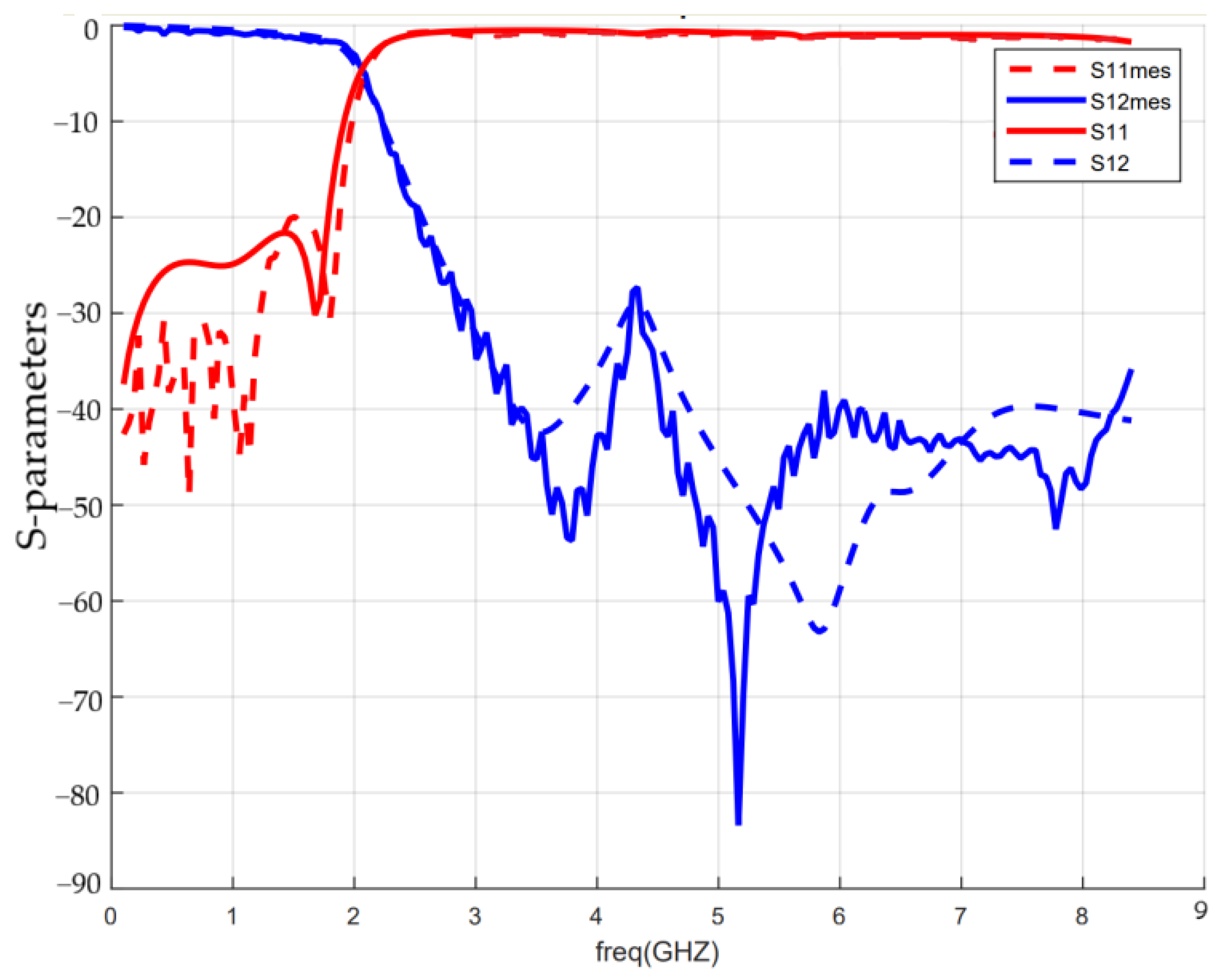
Figure 12 shows the measurement setup, while
Figure 13 compares the measured and simulated S-parameters. Good agreement is observed between the simulated and measured results in terms of cutoff frequency and attenuation level. Minor discrepancies are mainly attributed to fabrication tolerances, variations in the substrate dielectric parameters, and connector losses.
From
Figure 13, it can be seen that the simulated and measured S-parameters of the fabricated quasi-eight DGS low-pass filter exhibit close agreement, with the measured responses closely following the simulated characteristics. A strong agreement between the simulated and measured results is observed in the passband and near the cutoff frequency, where the insertion loss remains minimal. In addition, the stopband exhibits attenuation greater than 20 dB from 2.5 GHz to 8.5 GHz, confirming the effectiveness of the proposed DGS configuration. Minor deviations in the stopband region are mainly attributed to fabrication tolerances affecting the DGS slot dimensions, slight variations in the substrate dielectric properties, conductor losses, and connector-related imperfections. The small ripple sin the measured responses are primarily caused by impedance mismatches at the SMA interfaces and parasitic resonances introduced by the measurement setup, which are not fully captured in the EM simulation. Nevertheless, the overall filtering performance is well preserved, thereby validating the proposed design.
Consequently, the performance of the proposed DGS-LPF is summarized in
Table 4.
For a fair comparison among filters operating at different cutoff frequencies, the guided wavelength
was calculated at the cutoff frequency of each filter using Equation (4) [
12]
where
was approximated as (
+ 1)/2 for consistency [
12].
Table 4 presents a comparison of the electrical size between the proposed DGS-LPF and previously reported designs. Normalization with respect to
enables a frequency-independent assessment of compactness and provides a consistent basis for comparison.
As indicated in
Table 4, although some reported filters exhibit smaller normalized electrical areas, the proposed design achieves a competitive electrical size of 0.12
λg2 while maintaining excellent performance, including a return loss exceeding 26 dB and an insertion loss of only 0.3 dB. These characteristics demonstrate that the proposed structure provides an effective balance between compactness and electrical performance, making it suitable for compact microwave front-end applications.
Therefore, the proposed filter demonstrates a favorable trade-off between compactness and filtering performance.
7. Conclusions
A compact low-pass filter based on a quasi-eight-shaped defected ground structure (DGS) has been proposed and experimentally validated. By effectively modifying the ground-plane current distribution, the structure introduces additional equivalent inductance and capacitance, resulting in enhanced filtering performance and strong harmonic suppression. The fabricated prototype achieves a measured cutoff frequency of approximately 2.2 GHz, with an insertion loss lower than 1 dB in the passband and a wide stopband extending up to 8 GHz, providing attenuation exceeding 26 dB. The close agreement between the equivalent circuit model, full-wave electromagnetic simulations, and measured results confirms the reliability and practical feasibility of the proposed design. Owing to its compact planar structure, high stopband attenuation, and simple fabrication process, the proposed DGS low-pass filter represents a promising solution for microwave L-band systems, GPS applications, and radar front-end implementations.
Future work will focus on developing tunable and reconfigurable versions of the proposed DGS-based filter by incorporating adjustable geometrical parameters or active tuning elements, enabling dynamic control of the cutoff frequency and improved adaptability for modern microwave communication systems.
Author Contributions
Conceptualization, N.H.; Methodology, N.H.; Software, N.H.; Validation, N.H., D.F. and B.A.; Formal analysis, N.H.; Investigation, N.H.; Resources, N.H.; Data curation, N.H.; Writing—original draft, N.H.; Writing—review & editing, N.H.; Visualization, N.H.; Supervision, N.H.; Project administration, N.H., D.F. and B.A.; Funding acquisition, N.H. All authors have read and agreed to the published version of the manuscript.
Funding
This research received no external funding.
Data Availability Statement
Data are contained within the article.
Conflicts of Interest
The authors declare no conflict of interest.
References
- Ahn, D.; Park, J.S.; Kim, C.S.; Qian, Y.; Itoh, T. A Design of the low-pass filter using the novel micro strip defected ground structure. IEEE Trans. Microw. Theory Tech. 2001, 49, 86–91. [Google Scholar] [CrossRef]
- Boutejdar, A. Design of Compact Reconfigurable Broadband Band-Stop Filter Based on a Low-Pass Filter Using Half Circle DGS Resonator and Multi-Layer Technique. Prog. Electromagn. Res. C 2017, 71, 91–100. [Google Scholar] [CrossRef][Green Version]
- Lee, W.J.; Yoon, W.-S.; Ahn, D.; Han, S.-M. Compact Design Method for Planar Antennas with Defected Ground Structures. Electronics 2023, 12, 2226. [Google Scholar] [CrossRef]
- Dokmetas, B.; Arican, G.O.; Akcam, N.; Yazgan, E. A Compact Band stop Filter Design Using DMS-DGS Technique for Radar Applications. Appl. Comput. Electromagn. Soc. J. 2021, 36, 1460–1467. [Google Scholar]
- Hossen, M.R.; Ramzan, M.; Sen, P. Defected Ground Structure-based Compact Wideband Monopole Antenna Design with Equivalent Circuit Modeling for Communication and Sensing Applications. In Proceedings of the 2023 IEEE 3rd International Symposium on Joint Communications & Sensing (JC&S), Seefeld, Austria, 5–7 March 2023. [Google Scholar] [CrossRef]
- Vali, S.K.S.; Rao, K.S. Design of wide stopband lowpass filter using defected ground structure. Microsyst. Technol. 2024, 30, 721–728. [Google Scholar] [CrossRef]
- Boutejdar, A.; Amzi, M.; Bennani, S.D. Design and Improvement of a Compact Band-pass Filter using DGS Technique for WLAN and WiMAX Applications. TELKOMNIKA 2017, 15, 1137–1144. [Google Scholar] [CrossRef]
- Al Sharkawy, M.; Luxor, O.; Boutejdar, A.; Alhefnawi, F. Improvement of Compactness of Lowpass/Bandpass Filter Using a New Electromagnetic Coupled Crescent Defected Ground Structure Resonators. Appl. Comput. Electromagn. Soc. J. 2010, 25, 570–577. [Google Scholar]
- Koo, J.-J.; Oh, S.; Hwang, M.-S.; Park, C.; Jeong, Y.; Lim, J.; Choi, K.-S.; Ahn, D. A new DGS unequal power divider. In Proceedings of the 37th European Microwave Conference, Munich, Germany, 8–12 October 2007; pp. 556–559. [Google Scholar]
- Boutejdar, A.; Omar, A.; Burte, E.P.; Mikuta, R. An Improvement of Defected Ground Structure Lowpass/Bandpass Filters Using H-Slot Resonators and Coupling Matrix Method. J. Microw. Optoelectron. Electromagn. Appl. 2011, 10, 295. [Google Scholar] [CrossRef]
- Zhang, J.; Yang, R.; Zhang, C. High-Performance Low-Pass Filter Using Stepped Impedance Resonator and Defected Ground Structure. Electronics 2019, 8, 403. [Google Scholar] [CrossRef]
- Pozar, D.M. Microwave Engineering, 4th ed.; John Wiley & Sons: Hoboken, NJ, USA, 2012. [Google Scholar]
- Boutejdar, A.; Ibrahim, A.A.; Burte, E.P. Design of a Novel UltrawideStopbandLowpass Filter Using a DMS-DGSTechnique for Radar Applications. Int. J. Microw. Sci. Technol. 2015, 2015, 101602. [Google Scholar] [CrossRef]
- Lu, K.; Wang, G.M.; Wang, Y.W.; Yin, X. An improved design of Hi-Lo micro strip low pass filter using uniplanar double spiral resonant cells. Prog. Electromagn. Res. Lett. 2011, 23, 89–98. [Google Scholar] [CrossRef]
- Yang, M.; Xu, J.; Zhao, Q.; Peng, L.; Li, G. Compact, broad-stopband low pass filters using sirs-loaded circular hairpin resonators. Prog. Electromagn. Res. 2010, 102, 95–106. [Google Scholar] [CrossRef]
- Li, J.-L.; Twumasi, B.A.; Chen, R.-B.; Gao, S.-S. Compact log-periodic microstrip DGS filters with high figure-of-merit. J. Electr. Eng. 2024, 75, 411–417. [Google Scholar] [CrossRef]
| Disclaimer/Publisher’s Note: The statements, opinions and data contained in all publications are solely those of the individual author(s) and contributor(s) and not of MDPI and/or the editor(s). MDPI and/or the editor(s) disclaim responsibility for any injury to people or property resulting from any ideas, methods, instructions or products referred to in the content. |