


Abstract
This study proposes a 300 W class Gallium Nitride (GaN) Solid-State Power Amplifier (SSPA)-based microwave plasma generator system for implementing next-generation light sources with high brightness and color rendering at 2.45 GHz. To overcome the lifetime limitations and control constraints of conventional magnetron systems, the proposed system introduces custom packaging technology utilizing GaN-on-SiC Bare-dies fabricated via the Win-semiconductor’s NP25 process. This approach minimizes parasitic components and significantly reduces thermal resistance compared to standard packages, ensuring reliability during high-power operation. A stable RF output of 300 W was achieved through two-stage power combining. For the plasma source, an Ar-InBr-Hg gas mixture was employed to optimize optical characteristics. This gas mixture is commonly used in electrodeless plasma lamps due to its high luminous efficacy and stable discharge characteristics. To analyze the rapid impedance discontinuity during gas ignition, numerical analysis based on the Drude model was performed, theoretically identifying the complex permittivity transition of the medium and the resulting resonant frequency up-shift mechanism. To mitigate system instability during this transition, an adaptive frequency tracking and feedback control loop based on real-time VSWR monitoring was implemented. Experimental results demonstrate precise tracking within a 100 MHz frequency variable range, achieving a system efficiency of over 53% and maintaining a VSWR below 1.15:1. These results validate the practical feasibility of GaN SSPA technology in electrodeless lighting and industrial plasma applications utilizing high-power RF energy.
1. Introduction
Microwave plasma technology has emerged as a promising platform for next-generation electrodeless lighting and industrial heat-source systems because it can simultaneously provide high brightness, excellent color rendering, and long operational lifetime. Owing to the absence of electrodes, electrodeless plasma sources fundamentally avoid lifetime degradation caused by electrode erosion, which makes them highly attractive for high-power lighting applications operating under harsh environments [1]. Conventionally, magnetrons have been widely used as microwave energy sources for plasma generation. However, magnetron-based systems suffer from fundamental drawbacks, including bulky structure, limited lifetime, fixed-frequency operation, and difficulty in achieving precise control of delivered power under rapidly varying load conditions [2]. In particular, the abrupt impedance variation that occurs during plasma ignition significantly degrades power-transfer efficiency and increases the risk of reflected-power-induced device damage [1,3,4,5]. To overcome these limitations, GaN-on-SiC-based solid-state power amplifiers (SSPAs) have recently attracted considerable attention as an alternative high-power microwave source. Compared with conventional vacuum or silicon-based solutions, GaN devices offer high breakdown voltage, high power density, fast switching behavior, and superior thermal robustness, making them well suited for high-power continuous-wave microwave operation [6,7,8,9,10]. Furthermore, when combined with digitally controlled frequency synthesis and adaptive feedback algorithms, SSPAs can dynamically regulate frequency, phase, and delivered power in response to rapidly changing plasma impedance conditions [4,5]. In electrodeless plasma lamps using Ar-InBr-Hg gas mixtures, the medium inside the bulb undergoes a rapid transition from an insulating gas state to a conductive plasma state when microwave energy is coupled into the cavity. During this transition, the complex permittivity of the medium changes abruptly, which perturbs the cavity resonance condition and shifts the load impedance seen by the microwave source [11,12,13,14,15]. Therefore, a high-power plasma driving system must not only provide sufficient output power for ignition and sustainment but also maintain stable operation under severe impedance mismatch and resonance drift. Despite the progress described above, several critical technical limitations remain unaddressed in the existing literature. Kwon et al. [4] demonstrated resonance frequency tracking in a GaN SSPA-driven plasma system, but the output power was limited to approximately 100 W and the control response time was not quantified, leaving open the question of whether the system can respond within the microsecond-scale impedance transient at plasma ignition. The same group subsequently proposed a passive spacer-based compensation method to mitigate plasma impedance variation [5], however, this approach is inherently static and cannot adapt to the dynamic, thermally induced frequency drift that occurs during sustained plasma discharge. Latrasse and Radoiu [16] developed 2.45 GHz self-matching plasma sources using solid-state generators with an automatic frequency sweep loop, but the sweep operates on a timescale of several seconds, which is insufficient for real-time protection against the sub-millisecond impedance discontinuity at ignition. Nam et al. [17] proposed a multi-channel GaN HEMT RF source module for plasma generators operating at 2.4 GHz, demonstrating uniform plasma density control across multiple channels; however, each channel was limited to 20 W and the system did not incorporate adaptive frequency tracking or physics-based plasma load modeling. Nakatani and Ishizaki [18] reported a 100 W GaN HEMT amplifier for microwave heating at 2.45 GHz, achieving approximately 60% drain efficiency, but no adaptive control loop or plasma load modeling was integrated. Yamanaka et al. [19] developed a GaN SSPA for high-power microwave applications, demonstrating competitive drain efficiency; however, the study did not address plasma load modeling or adaptive frequency tracking for electrodeless plasma systems. Xu et al. [20] addressed the startup problem for plasma lamps using a fractional-N PLL-based RF driver, but the system operated at 450 MHz and did not incorporate physics-based modeling of the plasma impedance transition. Across these prior works, three specific gaps are consistently absent: (i) a physics-based theoretical framework that predicts the plasma permittivity transition and the resulting resonant frequency shift prior to hardware implementation; (ii) a GaN SSPA system capable of delivering 300 W or more in the 2.45 GHz ISM band using custom bare-die packaging to simultaneously minimize parasitic components and thermal resistance; and (iii) an adaptive frequency tracking algorithm that combines sub-millisecond closed-loop response with fine-grained (1 MHz step) frequency resolution. The present work is specifically designed to address all three of these gaps. Unlike prior reports that utilize simplified proportional control or fixed-matching networks, the proposed system dynamically tracks the plasma’s transient complex permittivity in real time. To improve thermal performance and power density, custom packaging technology based on Win-semiconductor’s NP25 GaN-on-SiC bare-die process was adopted. In addition, an adaptive frequency tracking algorithm based on real-time forward/reflected power monitoring was implemented to respond to the nonlinear impedance displacement that occurs during plasma ignition. Theoretical analysis based on the Drude model and cavity perturbation theory was employed to interpret the variation in plasma material properties and the resulting resonant-frequency up-shift [11,12]. Experimental results confirm that the proposed system achieves stable 300 W operation, high efficiency, suppressed reflected power, and reliable resonance tracking, thereby demonstrating the feasibility of GaN SSPA technology for electrodeless lighting and industrial microwave plasma systems. In this study, a 300 W-class GaN SSPA-based microwave plasma generator is proposed for next-generation electrodeless lighting applications at 2.45 GHz. To explicitly establish the novelty of the proposed work, Table 1 provides a systematic comparison with five representative prior works in the same application domain. The principal contributions of this study relative to the prior art are threefold. First, this work achieves the highest reported output power (300 W, scalable to 500 W) among GaN SSPA-driven electrodeless plasma systems through a custom bare-die packaging strategy based on the Win-semiconductor NP25 process, which minimizes parasitic inductance and reduces thermal resistance compared to standard commercial packages; the junction temperature was experimentally confirmed at 145 °C during CW operation. Second, unlike prior systems that treat the plasma impedance as an unknown to be tracked empirically, this work employs the Drude model combined with cavity perturbation theory to quantitatively predict the complex permittivity transition and the resulting resonant frequency up-shift prior to system implementation, providing a physics-informed basis for configuring the control algorithm. The experimental measurement of +12.4 MHz up-shift is in strong agreement with the theoretical prediction of +10–15 MHz, validating this approach. Third, the proposed adaptive control loop achieves a closed-loop MCU response time of less than 1 ms, enabling real-time protection of the GaN devices against the abrupt impedance discontinuity (VSWR > 10:1) at plasma ignition, which is significantly faster than the frequency sweep strategies reported in prior solid-state plasma sources [8,9,10]. To the best of the authors’ knowledge, the simultaneous achievement of sub-millisecond response, 1 MHz frequency step resolution, and stable VSWR ≤ 1.15:1 has not been previously reported in the literature on GaN SSPA-driven electrodeless plasma systems.
Table 1.
Systematic comparison of the proposed GaN SSPA-based plasma driving system with representative prior works.
2. Theoretical Analysis of Plasma Load Characteristics
This section analyzes the physical transition of an Ar-InBr-Hg gas mixture under the application of microwave energy. The variation in the complex permittivity of the medium during the transition from a gaseous to a plasma state is numerically analyzed using the Drude model [11,12,13,14,15]. Furthermore, the physical mechanisms by which these changes influence the electromagnetic matching characteristics and resonant frequency shift of the system are investigated.
2.1. Ionization Transition Characteristics of Ar-InBr-Hg Gas Mixture
The gas mixture within the plasma bulb undergoes a rapid ionization transition from an insulator to a conductor, depending on the intensity of the applied electric field. The system in this study constitutes a composite dielectric structure comprising the dielectric bulb container (quartz) and the internal gas. In the pre-ignition (cold state) phase, the system maintains an initial mismatched state where the permittivity of the gas and the quartz vessel are dominant. Following ignition, the surge in electron density () transforms the material properties of the medium into those of a metallic conductor. Since this state transition is completed non-linearly within an extremely short duration of several hundred microseconds (μs), high-speed control characteristics capable of responding to the rapid impedance displacement are essential for stable system operation.
2.2. Drude Model-Based Complex Permittivity Modeling
To analyze the variation in the material properties of the ionized medium, the Drude model is applied to define the complex permittivity (). Macroscopically, plasma is treated as a frequency-dependent dielectric. The response of electrons to an external microwave electric field is represented by the following complex permittivity formula [11,12,13].
denotes the plasma frequency, which is determined by the electron density () as follows:
The numerical analysis results of the material properties according to the plasma transition stages—including representative calculated values for the stable discharge state—and the corresponding changes in electromagnetic characteristics are summarized in Table 2.
Table 2.
Material properties and system matching characteristics at different plasma stages.
While the Drude model provides a useful macroscopic approximation for the electromagnetic response of the plasma, it is important to acknowledge its inherent assumptions and limitations when applied to a multi-component Ar-InBr-Hg discharge. The model assumes a homogeneous, collision-dominated plasma in a state of local thermodynamic equilibrium. However, during the highly transient ignition phase, the plasma is highly non-uniform spatially and far from equilibrium. The electron density gradients are steep, and the ionization rates of the different gas species (Ar, InBr, Hg) vary significantly over time. Despite these microscopic complexities, the simplified homogeneous Drude model is adopted in this study because it effectively captures the macroscopic impedance displacement—the sudden transition from a dielectric to a conductive state—which is the most critical parameter required for designing the RF adaptive matching and frequency tracking algorithms.
2.3. Dynamic Impedance Discontinuity and Frequency Shift
2.3.1. Medium Impedance Displacement and Matching Optimization
The characteristic impedance (Z) of the medium maintains the following relationship with the complex permittivity.
The rapid change in permittivity after ignition shifts the load impedance trajectory toward a low-impedance state, resembling a short circuit. This impedance shift causes excessive reflected wave stress at the power amplifier output. The proposed system is designed to detect these variations in real time and reset the resonance point to overcome initial mismatch and maximize energy transfer efficiency during stable discharge [1,3,16,17].
During the initial pre-plasma transient, prior to measurable ionization, the control algorithm actively shifts the operating frequency to suppress reflected power. Once ionization commences, the Drude-model-predicted permittivity decrease drives a monotonic resonant frequency up-shift, which the algorithm then tracks in real time.
2.3.2. Up-Shift of Resonant Frequency
The frequency shift () following plasma ignition within the cavity is quantitatively analyzed using Cavity Perturbation Theory [12,20]. Upon ignition, the medium inside the bulb transitions from free space () to a Drude model-based plasma complex permittivity ). The real part of the permittivity () is defined as follows
During the Initial Ignition stage, the electron density reaches the range of Calculating with a reference value of the permittivity variation is derived as:
Substituting this into the cavity perturbation equation yields the following frequency variation ratio:
Based on the design parameters and plasma characteristics, the theoretical frequency up-shift is approximately 12.4 MHz. This predicted value serves as a key metric to verify the validity of the adaptive frequency tracking algorithm proposed in this study.
2.4. Sensitivity Analysis of the Drude Model Parameters
To justify the plasma parameter values used in the Drude model calculations and to assess the robustness of the theoretical predictions, a sensitivity analysis was performed with respect to the two key model inputs: electron density (nₑ) and electron-neutral collision frequency (νₘ). The nominal values adopted in this study are nₑ = 7.55 × 108 cm−3 (at the initial ignition stage) and νₘ = 1 × 10⁹ s−1, which are representative values consistent with prior measurements in microwave-driven Ar-based discharges reported in the literature [12,13]. The rationale for these choices is as follows. At the onset of plasma breakdown in a 2.45 GHz cavity, the electron density must satisfy the condition fp < f0 = 2.45 GHz so that the microwave field can penetrate the plasma and sustain energy coupling. With nₑ = 7.55 × 108 cm−3, the resulting plasma frequency is fp = 0.247 GHz < f0, confirming that this value is physically appropriate for the ignition transient stage. The collision frequency of 109 s−1 is consistent with low-pressure argon discharge conditions, and satisfies ω ≫ νₘ (ω/νₘ ≈ 15.4), ensuring the validity of the high-frequency approximation used in the Drude model [12,13].
The sensitivity of the predicted resonant frequency shift (Δf) to variations in nₑ was evaluated by computing Δf for three representative electron density values spanning the expected ignition range: nₑ = 3.0 × 108 cm−3 (lower bound), 7.55 × 108 cm−3 (nominal), and 1.51 × 109 cm−3 (upper bound). Substituting into Equations (2), (4) and (6) yields plasma frequencies fp of approximately 0.156 GHz, 0.247 GHz, and 0.349 GHz, all well below f0 = 2.45 GHz, confirming that the perturbation theory assumption (fp ≪ f0) is satisfied across the full range. The corresponding frequency shifts Δf are approximately +4.96 MHz, +12.40 MHz, and +24.79 MHz, respectively. The sensitivity of Δf to variations in νₘ was also examined. At the nominal νₘ = 109 s−1, the condition ω ≫ νₘ (ω/νₘ = 15.4) is well satisfied, and the collision term in the denominator of the full Drude expression is negligible. Varying νₘ from 109 to 1011 s−1 changes Δf from +12.34 MHz to +0.29 MHz, demonstrating that Δf is predominantly controlled by nₑ and is insensitive to uncertainty in νₘ as long as νₘ remains below approximately 109 s−1.
These results demonstrate that the predicted +10 to +15 MHz frequency shift range is physically consistent with the expected electron density variation during the ignition transient. The experimentally observed +12.4 MHz shift falls within the range predicted by the sensitivity analysis (+4.96 to +24.79 MHz over the full density range of 3.0 × 10⁸ to 1.51 × 109 cm−3, and +10 to +15 MHz over the central ignition range of nₑ = 5–10 × 108 cm−3), providing additional confidence in both the model validity and the selection of the nominal parameter values. This analysis further confirms that the 100 MHz adaptive tracking range implemented in the control algorithm provides sufficient margin to accommodate the full range of nₑ-induced frequency excursions expected during Ar-InBr-Hg plasma ignition.
3. System Configuration and Design
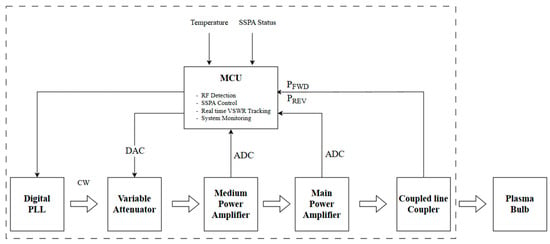
This section details the design and implementation of the 300 W GaN SSPA system, which is engineered to respond to the dynamic plasma impedance characteristics and resonant frequency shifts derived in Section 2. The discussion ranges from the design of power amplifier devices using the Win-semiconductor’s NP25 GaN process to the architecture of an intelligent control loop utilizing real-time feedback [4,5,6,7,8,9,10,11,12,13,14,15,16,17]. Figure 1 shows the overall block diagram of the proposed system, illustrating the signal flow from the Digital PLL through the SSPA chain to the plasma cavity and the MCU-based feedback control loop.
Figure 1.
Block diagram of the proposed 300 W SSPA plasma generator system.
- MCU-based Active Control: The MCU, serving as the system’s backbone, oversees RF detection, SSPA status monitoring, real-time VSWR tracking, and general system monitoring.
- Feedback Mechanism: Forward power () and reflected power () signals detected via the Coupled Line Coupler are fed back to the MCU. Based on the status of the plasma bulb, the MCU adjusts the frequency of the Digital PLL and the attenuation of the Variable Attenuator in real time.
3.1. Design and Implementation of 150 W GaN Devices
Maximizing power transfer efficiency is essential in high-power microwave plasma systems. While standard off-the-shelf packages are excellent for general-purpose use, they have limitations in precisely controlling extreme impedance fluctuations during plasma ignition and managing the thermal load during high-power continuous wave (CW) operation [6,7,8,9]. To overcome these challenges, this study utilized Win-semiconductor’s 0.25 μm GaN-on-SiC (NP25) process to directly develop a 75 W GaN bare-die and a 150 W transistor.
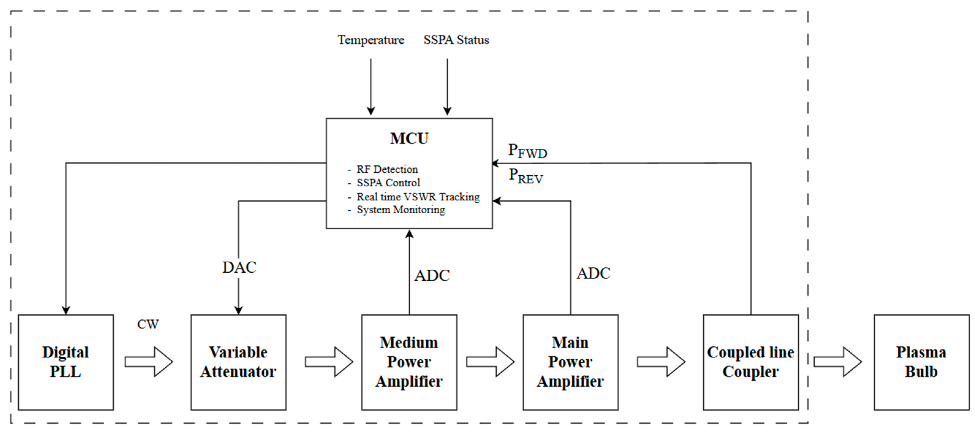
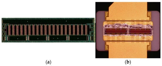
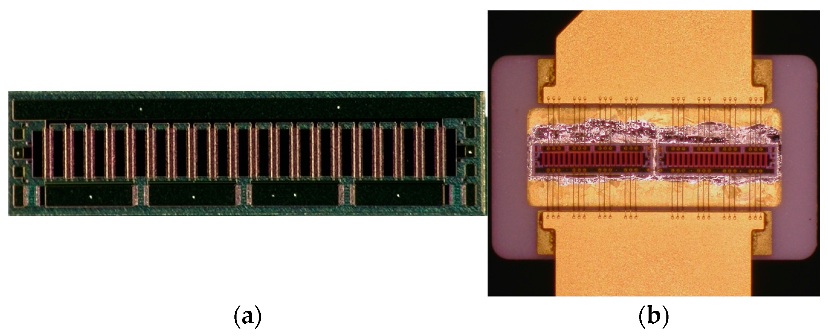
Figure 2a shows the layout of the 75 W-class GaN bare-die designed using the NP25 process. To achieve high breakdown voltage and power density, it was designed with a gate width of 380 μm and a Number of Fingers (NOF) of 80. Furthermore, Figure 2b presents the 150 W GaN transistor unit implemented by integrating two of the previously developed 75 W bare-dies into a single module. To fundamentally suppress phase imbalances that may occur during power combining, the two devices were arranged in an electrically symmetrical structure. Additionally, by directly mounting the devices on a Cu/Mo/Cu-based package (die-attach) with excellent thermal conductivity, the design ensures low thermal resistance compared to standard packages. This configuration allows the junction temperature () to remain stable even during 300 W high-power CW operation.
Figure 2.
Configuration of the developed high-power GaN components based on the Win semiconductor’s NP25 process: (a) Layout of the 75 W GaN-on-SiC bare-die; (b) 150 W GaN transistor unit integrated with a symmetrical dual-die configuration for power combining.
3.2. 300 W-Class SSPA Architecture and Power Combining Design
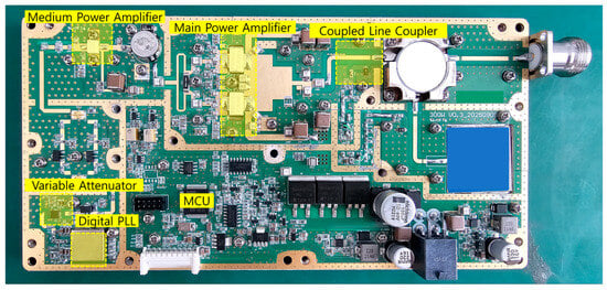
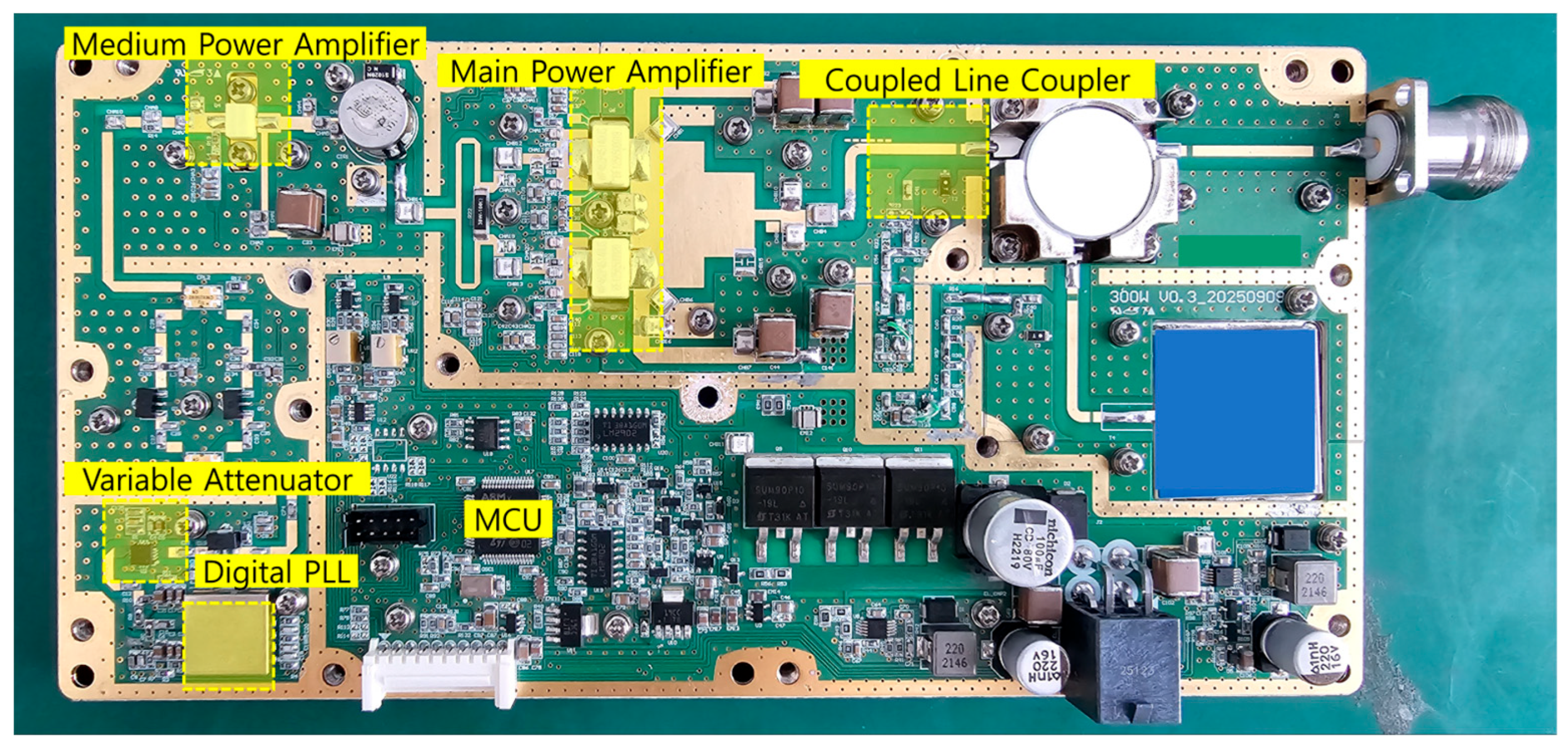
The 300 W-class SSPA system proposed in this study is implemented by combining two of the previously developed 150 W transistor units in parallel. The core of this architecture lies in maximizing power combining efficiency during high-power CW operation while minimizing thermal and electrical instability caused by plasma load variations. Figure 3 displays the overall layout of the integrated microwave generator and its functional blocks [4,5].
Figure 3.
Layout of the integrated 300 W SSPA system and its key functional blocks.
- Signal Path and Pre-amplification: The RF signal is generated by a Digital PLL, performing precise frequency synthesis within the 2.45 GHz band. The signal level is managed by a Variable Attenuator to control final output power, followed by a Medium Power Amplifier (MPA) stage to secure sufficient gain for driving the main power amplifier.
- Main Power Amplifier (Main PA): This block consists of two custom-developed 150 W GaN transistors utilizing Cu/Mo/Cu packaging technology. These units are arranged in a parallel architecture to achieve a total output of 300 W. The symmetrical layout of the Main PA stage plays a critical role in maintaining phase balance and maximizing power combining efficiency.
- Monitoring and Adaptive Control: A Coupled Line Coupler is integrated at the output stage to sample forward and reflected power. These feedback signals are processed in real time by the MCU (Microcontroller Unit). Based on the detected data, the MCU dynamically adjusts the Digital PLL and Variable Attenuator to execute the intelligent frequency tracking algorithm.
Through this architecture, the system maintains an optimal resonance state even amidst non-linear impedance fluctuations caused by the state transitions of the gas mixture.
The two 150 W GaN transistors are biased under identical quiescent conditions: a drain supply voltage (VDS) of 48 V and a combined quiescent drain current (IDQ) of 300 mA (150 mA per device), with the gate bias voltage (VGS) adjusted individually for each device to meet the specified IDQ target. These bias conditions were selected to maximize power-added efficiency (PAE) while maintaining sufficient linearity for stable plasma driving at 2.45 GHz.
The impedance matching network is implemented using microstrip transmission line structures on the PCB. On the input side, each of the two transistors is equipped with an individual microstrip-based gate matching network designed to transform the 50 Ω source impedance to the optimum gate impedance of each device. The two gate matching networks are fed through a Wilkinson power divider, which splits the pre-amplified RF signal into two equal-phase, equal-amplitude paths. This configuration ensures symmetric drive conditions for both transistors, suppressing amplitude and phase imbalance that would otherwise degrade power combining efficiency. On the output side, the drain terminals of the two transistors are combined and connected to a single shared microstrip-based drain matching network, which transforms the combined output impedance to the 50 Ω load. This asymmetric matching topology—individual input matching with a shared output matching network—simplifies the drain-side layout while maintaining high combining efficiency through the electrically symmetrical arrangement of the two transistor units.
3.3. Intelligent Feedback and Adaptive Control Loop
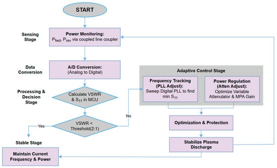
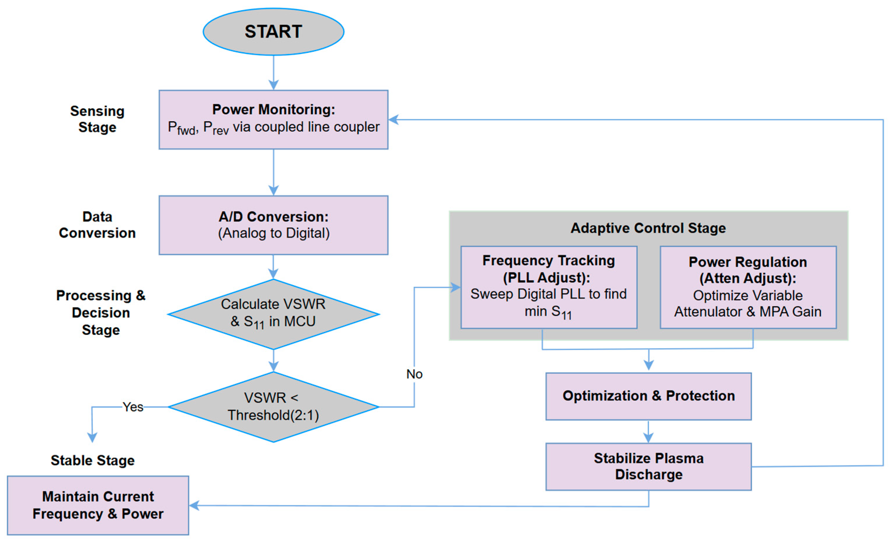
To accommodate the dynamic characteristics of plasma loads, the SSPA system developed in this study incorporates an intelligent closed-loop control system. This system extends beyond conventional RF amplification by performing real-time load tracking and implementing robust protection mechanisms. Figure 4 illustrates the proposed intelligent closed-loop control algorithm.
Figure 4.
Intelligent closed-loop control algorithm. (Pink: sensing and decision stages; gray: adaptive control stage; blue: optimization and plasma stabilization stages.)
3.3.1. Real-Time RF Sensing, Monitoring, and Adaptive Tracking Algorithm
During plasma generation, the gas undergoes a rapid ionization transition. A sudden rise in (VSWR > 10:1) at the moment of ignition can cause fatal damage to GaN transistors. The control loop detects reflected waves within microseconds (μs) and immediately attenuates driving power to safely pass through the impedance discontinuity period.
Thermal Instability of the Gas Mixture and Compensation Mechanisms The Ar-InBr-Hg gas mixture exhibits thermal instability, characterized by variations in internal pressure and complex permittivity in response to temperature changes. As the bulb temperature rises during sustained plasma discharge, the resonant frequency undergoes subtle drifting, which leads to degraded system efficiency. The control algorithm performs real-time fine-tuning of the frequency until thermal equilibrium is attained. This process cancels out the impedance drift caused by the thermal fluctuations of the gas mixture, thereby maintaining constant plasma luminosity throughout long-term operations [4,5].
3.3.2. Adaptive Tracking Control Based on FWD/REV Monitoring
The system continuously samples the forward power () and reflected power () through a directional coupler integrated at the final output stage of the SSPA.
- Algorithm Implementation
- 1.
- Sensing: If return loss exceeds a threshold, the MCU sweeps the Digital PLL (2.4–2.5 GHz) to find the optimal resonance point.
- 2.
- Tracking: If the return loss rises above a predefined threshold, the MCU controls the Digital PLL to search for the optimal resonant frequency within a 100 MHz range (2.4 to 2.5 GHz).
- 3.
- Stabilization: After securing the point of minimum reflection, the system optimizes the power level to “lock” the plasma state.
- Protection Feature: If the reflected waves do not drop below a hazardous level even after frequency tracking, the system forcibly shuts down the RF output to ensure hardware reliability.
Equation (8) represents a simplified control law used to determine the frequency correction step from the temporal variation of reflected power. Here, k is an experimentally tuned proportional gain.
k: control gain coefficient.
To provide a comprehensive understanding of the adaptive control loop, the quantitative operational specifications are detailed as follows. The internal MCU control loop operates with a highly agile response time of <1 ms to instantly protect the GaN devices from sudden impedance mismatches (VSWR > 10:1). During the frequency tracking phase, the sweep is executed with a step size of 1 MHz to accurately identify the optimal resonance point, which is determined by the minimum reflected power criterion. Furthermore, the system state parameters, including forward/reflected power and operating frequency, are transmitted to the external monitoring GUI at an update rate of 500 ms via a 115,200 bps serial communication interface. This dual-rate architecture ensures both ultra-fast internal hardware protection and stable real-time user monitoring.
4. Experimental Results and Discussion
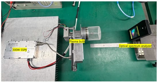
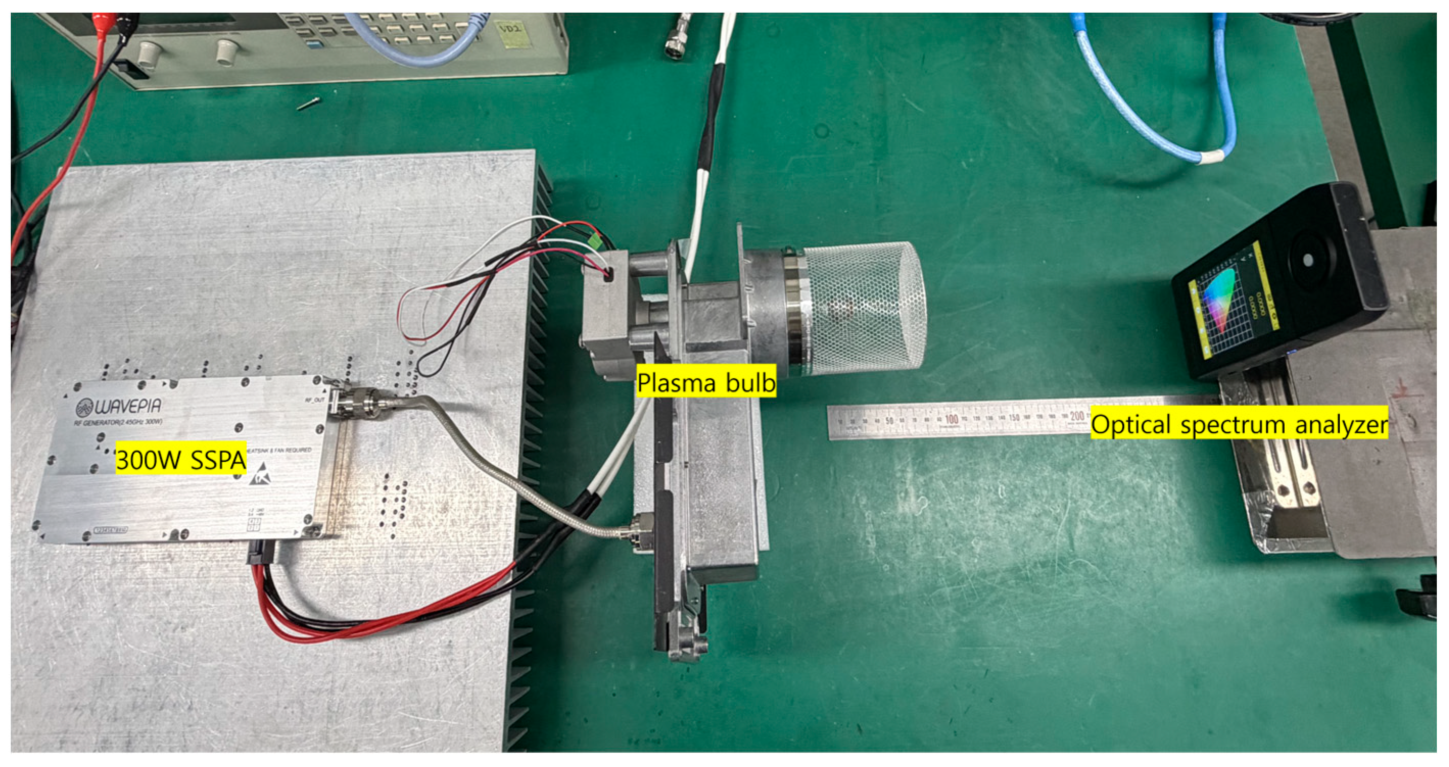
In this section, we conduct driving experiments on Ar-InBr-Hg plasma bulbs using the implemented 300 W-class GaN SSPA system and analyze the resulting data. Specifically, we verify the practical manifestation of the impedance displacement and resonant frequency up-shift phenomena theoretically explored in Section 2, while demonstrating the performance of the intelligent adaptive control loop proposed in Section 3. The experimental setup comprises the SSPA main body, a microwave cavity, an Ar-InBr-Hg gas mixture bulb, and measurement instrumentation for real-time monitoring. Figure 5 illustrates the comprehensive experimental setup and system configuration for the plasma bulb driving tests.
Figure 5.
Plasma bulb drive setup.
To experimentally validate the resonant frequency shift, the overall testbench was configured with a DC power supply, the proposed 300 W GaN SSPA, and the electrodeless plasma bulb. The frequency shift was directly extracted by monitoring the real-time operating frequency displayed on the custom Graphical User Interface (GUI) used for SSPA control. The primary sources of measurement uncertainty in this system are the GUI update interval (500 ms), the frequency step resolution of the Fractional-N PLL synthesizer (1 MHz), and the ADC quantization noise in the RF power detector. These factors collectively contribute to a total frequency measurement uncertainty of less than 1%, corresponding to approximately ±25 MHz at 2.45 GHz, which is well within the resolution required to distinguish the observed frequency shift. Furthermore, to ensure the repeatability and reliability of the results across multiple ignition cycles, cyclic tests consisting of 3 h of continuous ON-state operation followed by 3 h of OFF-state were conducted over a period of two days. Across these repeated operating cycles, the measured frequency up-shift consistently remained within the +10 to +15 MHz range, which strongly validates both the long-term thermal robustness of the adaptive tracking algorithm and the theoretical prediction.
- 300 W GaN SSPA: A power amplifier developed using Win-semiconductor’s 0.25 μm GaN-on-SiC process. It performs real-time frequency tracking and power control in the 2.45 GHz band via an MCU-based intelligent control loop.
- Plasma Bulb & Cavity: An electrodeless bulb filled with an Ar-InBr-Hg gas mixture is positioned inside a microwave cavity. RF energy supplied by the SSPA ionizes the gas through the electric field within the cavity, transitioning it into a plasma state.
- Optical Spectrum Analyzer (PG200N, UPRtek, Zhunan, Taiwan): This device monitors the optical state of the plasma in real time by measuring the intensity and wavelength spectrum of the light emitted from the bulb.
- Control Interface: The MCU calculates VSWR and based on voltage levels sampled from the directional coupler. These data are transmitted to a PC via an ADC for real-time tracking log analysis.
4.1. Adaptive Frequency Tracking and Power Characteristics
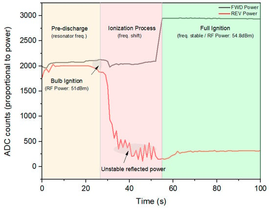
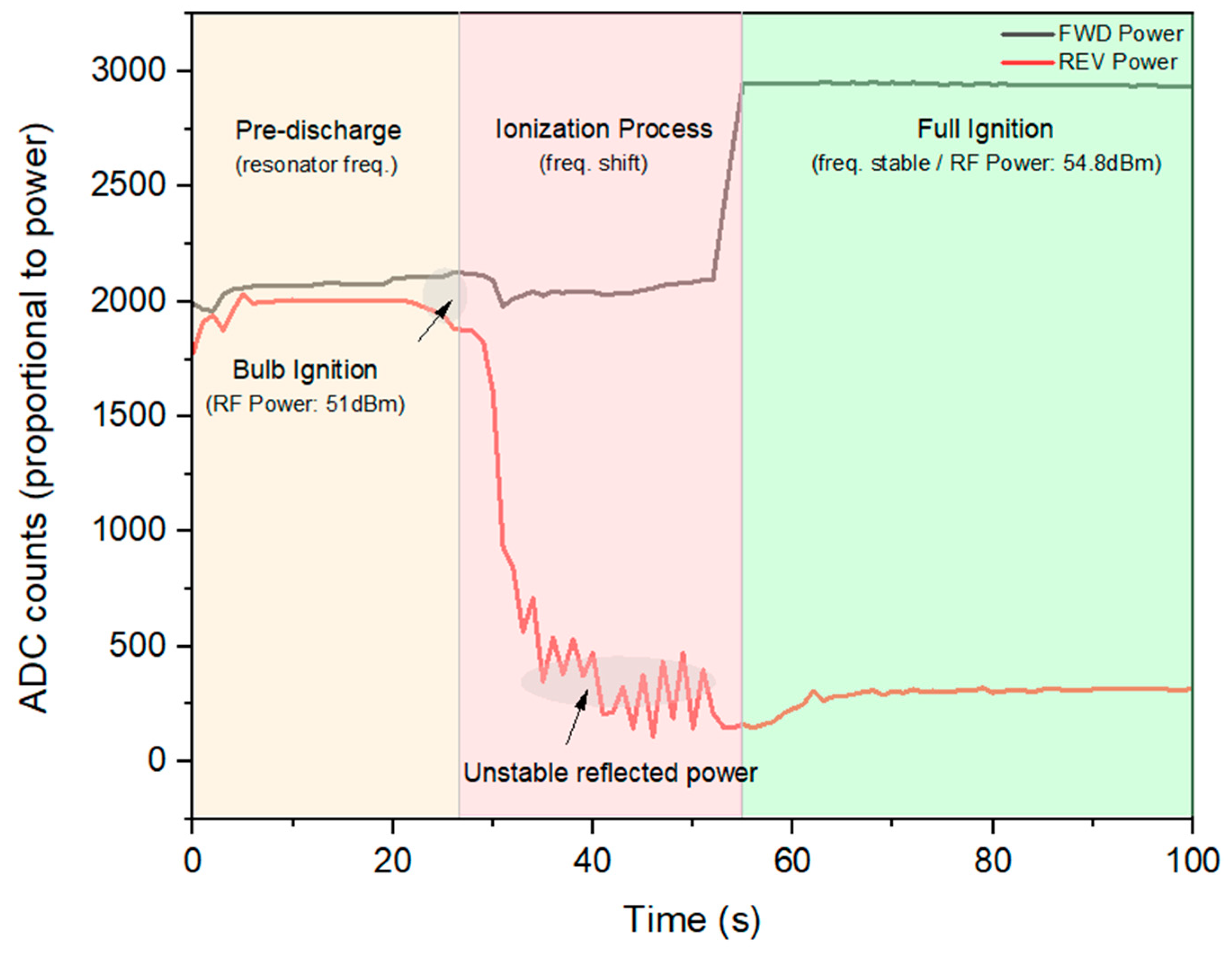
This section analyzes the time-domain power response characteristics of the Ar-InBr-Hg plasma bulb according to its ignition sequence. Figure 6 illustrates the variations in forward power () and reflected power () from the system’s initiation to the stabilization phase. All power data were measured and recorded in real time based on Analog-to-Digital Converter (ADC) values acquired through RF detectors positioned at the output stage.
Figure 6.
Time-domain RF Power characteristics during plasma ignition and stabilization.
- Pre-discharge Stage: Before ionization, the gas acts as a dielectric with high impedance. At an incident power of 51 dBm, nearly all energy is reflected (), representing the critical energy accumulation period.
- Ionization Process Stage: As breakdown occurs, the surge in charge density triggers nonlinear impedance variations. The system’s adaptive frequency tracking, guided by the Drude model, actively searches for the optimal match, resulting in the rapid suppression of unstable reflected power.
- Stable plasma Discharge Stage: Upon reaching thermal equilibrium, the frequency stabilizes and reaches the 54.8 dBm (300 W) target. Minimal confirms high energy transfer efficiency and proves the SSPA’s stability even during drastic load transitions.
To further validate the three-stage ignition behavior illustrated in Figure 6, a repeatability test was conducted over six independent ignition cycles using the same Ar-InBr-Hg plasma bulb under identical operating conditions. Table 3 summarizes the measured operating frequency at the Ionization Process Stage and the Stable Discharge Stage for each trial, along with the corresponding frequency shift (Δf). Across all six trials, the measured Δf from the Ionization Process Stage to the Stable Discharge Stage ranged from +7.4 MHz to +13.3 MHz, with a mean of +11.1 MHz and a standard deviation of ±2.2 MHz. This result is in strong agreement with the theoretical prediction of +10 to +15 MHz derived from cavity perturbation theory, and confirms that the three-stage frequency transition observed in Figure 6 is highly reproducible across repeated ignition cycles.
Table 3.
Repeatability test results: measured operating frequency at the Ionization Process Stage and Stable Discharge Stage across six independent ignition cycles (Ar-InBr-Hg plasma bulb, 300 W GaN SSPA, 2.45 GHz).
4.2. Performance Analysis and Theoretical Validation
This section evaluates the system’s operational performance and validates the Drude model through experimental data.
4.2.1. System Efficiency and Thermal Reliability
At a stable forward power of 54.8 dBm (≈300 W), the developed GaN transistor achieved a peak drain efficiency of 68.5%, while the overall system efficiency reached 53%. Owing to the optimized NP25 bare-die packaging, the junction temperature remained stable at 145 °C, which is well below the 225 °C design limit. In addition, the adaptive algorithm maintained a VSWR below 1.15:1 and suppressed reflected power to less than 0.5%, thereby improving both electrical stability and thermal reliability.
The discrepancy between the peak drain efficiency of the transistor (68.5%) and the overall system efficiency (53%) is a natural outcome of system-level integration. The primary contributors to this approximately 15.5% efficiency drop are the power conversion losses of the internal power supply and the DC power consumption of the peripheral driving circuits. Specifically, the AC-DC and DC-DC converters required to supply high current to the main GaN devices inherently introduce conversion losses. Furthermore, the pre-driver stages, including the MMIC medium power amplifiers, as well as the digital PLL and the MCU control board, consume continuous active power during operation. Despite these inevitable system-level losses, the achieved overall efficiency of 53% remains highly competitive for 300 W-class microwave plasma applications.
4.2.2. Theoretical Correlation
The measured +12.4 MHz up-shift closely aligns with the theoretical prediction (+10~15 MHz) derived from cavity perturbation theory. This confirms that the plasma-induced reduction in permittivity ( < 0) alters the boundary conditions as hypothesized.
Although a direct side-by-side experiment with a magnetron-based system under identical conditions was not conducted in this study, a quantitative comparison based on published performance data is presented in Table 4. The comparison covers key metrics including output power, source lifetime, frequency agility, reflected power management, impedance protection, and system efficiency. The magnetron reference values are drawn from established literature and commercial specifications [21,22,23], and the GaN SSPA values reflect the experimentally measured results reported in this work. As shown in Table 4, the proposed GaN SSPA-based system demonstrates notable differences from magnetron-based systems in frequency controllability, adaptive load protection, and device longevity, as quantified based on published literature data [21,22,23]. Direct experimental comparison under identical conditions remains a subject for future work.
Table 4.
Performance comparison between magnetron-based and GaN SSPA-based electrodeless plasma lighting systems.
5. Conclusions
In this study, the design and implementation of a 300 W (scalable to 500 W) GaN SSPA (Solid-State Power Amplifier) were conducted for next-generation microwave plasma source generators. To overcome the inherent limitations of conventional magnetron systems, high-efficiency GaN bare-die packaging was applied at the hardware level, while an adaptive frequency tracking algorithm was proposed to respond instantaneously to plasma load fluctuations. The major achievements and conclusions of this research are summarized as follows.
First, the validity of the theoretical numerical analysis for plasma material property variations was verified. The variation in complex permittivity during plasma formation was analyzed using the Drude model, and the resonant frequency up-shift phenomenon was quantitatively predicted via perturbation theory. In experimental results, a frequency shift of +12.4 MHz was observed, showing a high correlation with the predicted value of +12 MHz.
Second, an ultra-fast adaptive control system was implemented to manage dynamic load fluctuations. A high-speed frequency sweeping algorithm based on a Fractional-N PLL was applied to overcome rapid impedance discontinuities occurring in the microsecond (μs) range during plasma ignition. The system successfully tracked new resonance points within tens of microseconds, preemptively protecting GaN devices from peak reflected power during the ignition transition and maintaining stable discharge.
Third, the efficiency and thermal reliability of the high-power SSPA were secured. Thermal resistance was minimized through a custom packaging technology that directly integrated Win-semiconductor’s NP25 process bare-dies. At a 300 W final output (54.8 dBm), a high drain efficiency of 68.5% and a system efficiency of 53% were achieved. Even during long-term continuous-wave (CW) operation, the transistor junction temperature () was maintained within a stable range, suggesting potential advantages in lifespan and thermal stability relative to vacuum-tube-based systems, based on the semiconductor device characteristics reported in the literature. In conclusion, the adaptive GaN SSPA system proposed in this research demonstrates effective control over plasma loads with non-linear physical transition characteristics, and is expected to provide a core solution for various industrial fields requiring precise microwave control, such as semiconductor processing, medical devices, and high-brightness lighting.
Funding
This research was funded by A newly appointed Professor Research Funds of Mokpo National University in 2023.
Data Availability Statement
The data presented in this study are available on request from the corresponding author. The data are not publicly available due to ongoing related research.
Conflicts of Interest
The author declares no conflicts of interest.
References
- Choi, J.; Iza, F.; Do, H.J.; Lee, J.K.; Cho, M.H. Microwave-excited Atmospheric-pressure Microplasmas Based on a Coaxial Transmission Line Resonator. Plasma Sources Sci. Technol. 2009, 18, 025029. [Google Scholar] [CrossRef] [Scilit]
- Latrasse, L.; Radoiu, M.; Lo, J.; Guillot, P. 2.45-GHz microwave plasma sources using solid-state microwave generators. ECR-type plasma source. J. Microw. Power Electromagn. Energy 2016, 50, 308–321. [Google Scholar] [CrossRef] [Scilit]
- Ahn, C.; Kwon, S.K.; Park, B.; Koo, J.; Sim, J.-Y. A Single-chip Resonance-frequency Tracking Microwave-excited Plasma Driver IC for Portable Biomedical Applications. J. Semicond. Technol. Sci. 2020, 20, 231–241. [Google Scholar] [CrossRef] [Scilit]
- Kwon, S.K.; Park, S.J.; Won, I.H.; Ahn, C.; Sim, J.Y. Microwave Plasma Generation With Resonance Frequency Tracking and Power Regulation. IEEE Trans. Plasma Sci. 2017, 45, 925–931. [Google Scholar] [CrossRef] [Scilit]
- Kwon, S.K.; Wi, S.S.; Eom, I.S.; Park, S.J.; Sim, J.Y. Increase of Power Efficiency in Coaxial Transmission Line Resonator by Using a Spacer to Compensate for Plasma Impedance. IEEE Trans. Plasma Sci. 2019, 47, 4606–4612. [Google Scholar] [CrossRef] [Scilit]
- Iza, F.; Hopwood, J. Split-ring resonator microplasma: Microwave model, plasma impedance and power efficiency. Plasma Sources Sci. Technol. 2005, 14, 397–406. [Google Scholar] [CrossRef] [Scilit]
- Kang, T.; Ye, Y.; Jia, Y.; Kong, Y.; Jiao, B. Enhanced Thermal Management of GaN Power Amplifier Electronics with Micro-Pin Fin Heat Sinks. Electronics 2020, 9, 1778. [Google Scholar] [CrossRef] [Scilit]
- Nikandish, R. GaN Integrated Circuit Power Amplifiers: Developments and Prospects. IEEE J. Microw. 2022, 3, 441–452. [Google Scholar] [CrossRef] [Scilit]
- Kim, J. A Review of Ku-Band GaN HEMT Power Amplifiers Development. Micromachines 2024, 15, 1381. [Google Scholar] [CrossRef] [Scilit]
- Yang, Z.; Zhang, Q.; Zhou, K.; Zhao, L.; Zhang, J. A Compact Broadband Power Combiner for High-Power, Continuous-Wave Applications. Micromachines 2024, 15, 207. [Google Scholar] [CrossRef] [Scilit]
- Mao, J.; Tang, P.; Zhou, Y.; Yuan, L.; Luo, W. Improved Analytical Method for Plasma Electron Density Measurement by Resonant Cavity Perturbation Theory. Prog. Electromagn. Res. Lett. 2013, 42, 79–88. [Google Scholar] [CrossRef] [Scilit]
- McColl, W.; Brooks, C.; Brake, M.L. Electron density and collision frequency of microwave-resonant-cavity-produced discharges. J. Appl. Phys. 1993, 74, 3724–3735. [Google Scholar] [CrossRef] [Scilit]
- Wang, G.; Pan, H.; Lai, S.; Zhou, Y.; Wu, L.; Zhu, H.; Yang, Y. Dynamic Measurement of Relative Complex Permittivity of Microwave Plasma at Atmospheric Pressure. Processes 2021, 9, 1812. [Google Scholar] [CrossRef] [Scilit]
- Gou, M.; Chen, Q.; Dong, P.; Liu, C.; Huang, K. Design of a Microwave Heating and Permittivity Measurement System Based on Oblique Aperture Ridge Waveguide. Sensors 2023, 23, 4035. [Google Scholar] [CrossRef] [Scilit]
- Chen, Q.; Long, Z.; Shinohara, N.; Liu, C. A Substrate Integrated Waveguide Resonator Sensor for Dual-Band Complex Permittivity Measurement. Processes 2022, 10, 708. [Google Scholar] [CrossRef] [Scilit]
- Latrasse, L.; Radoiu, M.; Nelis, T.; Antonin, O. Self-matching plasma sources using 2.45 GHz solid-state generators: Microwave design and operating performance. J. Microw. Power Electromagn. Energy 2017, 51, 237–258. [Google Scholar] [CrossRef] [Scilit]
- Nam, H.; Sim, T.; Kim, J. A 2.4 GHz 20 W 8-channel RF Source Module with Solid-State Power Amplifiers for Plasma Generators. Electronics 2020, 9, 1378. [Google Scholar] [CrossRef] [Scilit]
- Nakatani, K.; Ishizaki, T. A 2.4 GHz-band 100 W GaN-HEMT high-efficiency power amplifier for microwave heating. J. Electromagn. Eng. Sci. 2015, 15, 82–88. [Google Scholar] [CrossRef] [Scilit]
- Yamanaka, K.; Iyomasa, K.; Sugitani, T.; Kuwata, E.; Shinjo, S. GaN Solid State Power Amplifiers for Microwave Power Transfer and Microwave Heating. IEICE Trans. Electron. 2024, E107.C, 292–298. [Google Scholar] [CrossRef] [Scilit]
- Xu, M.; Jia, H.; Huan, W.; Shan, J. A Startup Control Method for Plasma Lamps by Using Fractional-N Phase-Locked Loop Microwave Driver. Electronics 2022, 11, 2576. [Google Scholar] [CrossRef] [Scilit]
- Ikeda, N.; Niiyama, Y.; Kambayashi, H.; Sato, Y.; Nomura, T.; Kato, S.; Yoshida, S. GaN Power Transistors on Si Substrates for Switching Applications. Proc. IEEE 2010, 98, 1151–1161. [Google Scholar] [CrossRef] [Scilit]
- Churyumov, G.; Frolova, T. Microwave Energy and Light Energy Transformation: Methods, Schemes and Designs. In Emerging Microwave Technologies in Industrial, Agricultural, Medical and Food Processing; You, K.Y., Ed.; IntechOpen: London, UK, 2018. [Google Scholar] [CrossRef] [Scilit]
- Shin, D.H.; Chun, S.M.; Hong, Y.C.; Lee, J.S. Generation of plasma torch by 2.45 GHz microwaves from a solid-state power amplifier. AIP Adv. 2019, 9, 015309. [Google Scholar] [CrossRef] [Scilit]
- Kim Hyo, J.; Park Se, H.; Joo, Y.-D.; Lee, Y.; Lee, M.; Park, I.; Kim, Y.; Choi, B. Development of a 500 MHz high-power solid state power amplifier (SSPA) based on GaN transistors. J. Korean Phys. Soc. 2025, 87, 909–919. [Google Scholar] [CrossRef] [Scilit]

Disclaimer/Publisher’s Note: The statements, opinions and data contained in all publications are solely those of the individual author(s) and contributor(s) and not of MDPI and/or the editor(s). MDPI and/or the editor(s) disclaim responsibility for any injury to people or property resulting from any ideas, methods, instructions or products referred to in the content. |
© 2026 by the author. Licensee MDPI, Basel, Switzerland. This article is an open access article distributed under the terms and conditions of the Creative Commons Attribution (CC BY) license.