


Abstract
This paper presents a dual-phase dual-path hybrid buck–boost (DPBB) converter with an offset-controlled zero-current detector for Li-ion battery applications. Compared with inductive buck–boost converters, the proposed hybrid converter has a continuous input current, reducing the input voltage (VIN) ripple, which is caused by the parasitic inductance of the bonding wire. The proposed switching operation of the DPBB topology shows a low inductor current ripple with the continuous output delivery current; therefore, the ripple of the output voltage (VOUT) is reduced with the efficiency improvement. Compared with the prior hybrid buck–boost converters, it supports the buck and boost modes only by adjusting the duty cycle, so this addresses the issues of mode transitions. The proposed work utilizes the dual-phase operation to lower the conduction loss and improve the dynamic range. The proposed offset-controlled zero-current detector compensates for the timing error owing to the propagation delay of the control signals to reduce the reverse current from the output. The chip is fabricated using a 180-nm BCD process. It regulates VOUT at 3.3 V with a wide VIN range of 2.8 V to 4.2 V. Peak efficiencies of 95.88% and 93.08% are achieved in the buck and boost modes, respectively, with 140 mΩ of inductor DC resistance.
1. Introduction
As the types and numbers of mobile devices increase, managing the rechargeable Li-ion batteries equipped in these devices has become an important research topic. Because the voltage of Li-ion batteries varies from 2.8 V to 4.2 V depending on the operating conditions, research on the stable regulation of an output voltage (VOUT) from various battery voltage levels has been widely conducted over the past several years. In particular, many hybrid buck–boost converters have been presented with various design approaches to overcome the drawbacks of conventional inductive buck–boost converters, such as discontinuous input current (IIN), output delivery current (iDLV), and a high average inductor current (iL).
Early hybrid buck–boost converters were primarily designed to achieve a continuous iDLV [1,2,3,4]. However, they utilized the conventional inductive buck configuration for the buck mode without using a flying capacitor (CF). Therefore, they still have all the drawbacks of inductive buck converters, such as discontinuous IIN and an average iL level higher than ILOAD. Moreover, these converters typically operate in more than two modes to support buck-boost operation, which results in complex mode transitions.
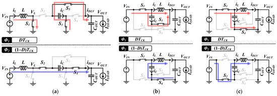
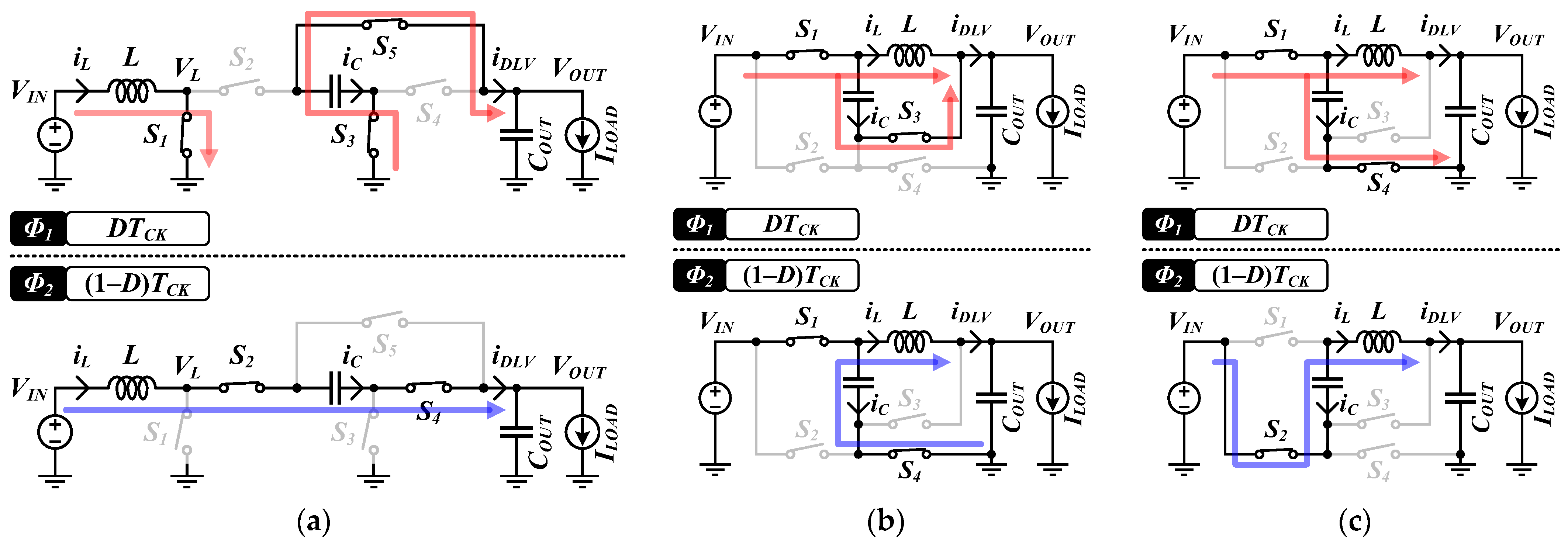
Figure 1 illustrates the operations of state-of-the-art hybrid buck–boost converters. To address the drawbacks of inductive buck–boost converters, prior hybrid DC–DC converters included the following two main design approaches: (1) topologies for dual current delivery paths [3,5,6,7,8,9,10,11] and (2) switched-inductor-capacitor topologies [1,2,9,10,11,12,13,14,15]. The dual-path current strategy supplies iDLV with iL and a capacitor current (iC). Figure 1a shows a state-of-the-art dual-path hybrid buck–boost (DPBB) converter [7]. Similar to the prior DPBB converter, the iDLV of certain hybrid DC–DC converters is composed of iL and iC alternately during a clock cycle (TCK) [5,7]. Otherwise, as shown in Figure 1b, other hybrid buck–boost converters have a reduced average iL by implementing a phase in which iDLV consists of both iL and iC simultaneously [6,8,9,10,11].
Figure 1.
Operations of prior methods; (a) DPBB converter in [7], (b) the buck mode, and (c) the boost mode of the four-phase hybrid buck-boost converter in [9].
The switched-inductor-capacitor topologies can be reconfigured to reduce the average iL by placing the inductor at either the input or output terminal depending on the boost or buck mode, respectively, as shown in Figure 1c [9]. The conventional inductive buck–boost and boost converters have discontinuous iL and iDLV; therefore, the average level of iL is always higher than the load current (ILOAD), causing a large conduction loss (PCD) owing to the DC resistance of the inductor (DCR) [16]. In inductive buck and boost converters, the inductor is placed at the input and output terminals, respectively. Consequently, depending on the voltage conversion ratio and the relationship between the input and output powers, both buck and boost converters exhibit an average iL higher than ILOAD. Therefore, they generally achieve lower power conversion efficiency than that of state-of-the-art hybrid DC–DC converters.
In addition to hybrid topology approaches, multiphase configurations provide an effective way to reduce the average iL level. Compared with single-phase DC–DC converters, multiphase configurations provide several advantages, such as low input and output ripples, fast load-transient response, and low iL [8,9,10,17,18]. As multiphase DC–DC converters have lowered iL levels for each inductor, they operate in discontinuous conduction mode (DCM) more often than single-phase DC–DC converters. Therefore, a highly accurate zero-current detector (ZCD) is required for an efficient operation. Many techniques have been proposed to detect the exact zero-crossing point of iL. Certain designs utilize voltage comparators to compare the voltage drops across the power switches to sense the zero-current point [19,20,21,22]. The resistance of the power switches must be increased to improve accuracy. However, this leads to efficiency loss. Therefore, they suffer from a tradeoff between timing error and efficiency.
Another approach is to detect the zero-crossing point of iL through an indirect voltage profile using digital circuits [23,24,25,26]. The exact switch-off timing is typically controlled with digitally controlled delay cells; however, they occupy a large silicon area. Moreover, the resolution of a digitally controlled ZCD is directly related to its accuracy. To increase the resolution, coarse and fine tuning of the delay cell was designed in [26], but this increases the circuit complexity.
To address the aforementioned issues, this paper presents a dual-phase dual-path DPBB architecture whose power stage is similar to that in [7], but with an additional phase (Φ3). The inclusion of Φ3 slightly improves the conduction loss and ripple characteristics by modifying the current flow and switching sequence. Furthermore, due to the dual-phase operation, the current flowing through each power stage is halved, which further reduces the overall conduction loss. In addition, an offset-controlled ZCD is employed to effectively minimize the power loss caused by reverse inductor current under light-load conditions. The remainder of this article is organized as follows. Section 2 describes the working principles and power loss analysis of the proposed DPBB operation. Section 3 presents the circuit implementation of the proposed method. Section 4 presents the measurement results of the fabricated chip. Finally, conclusions are presented in Section 5.
2. Proposed Dual-Path Hybrid Buck-Boost Operation
2.1. Proposed Power Stage Operation
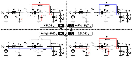
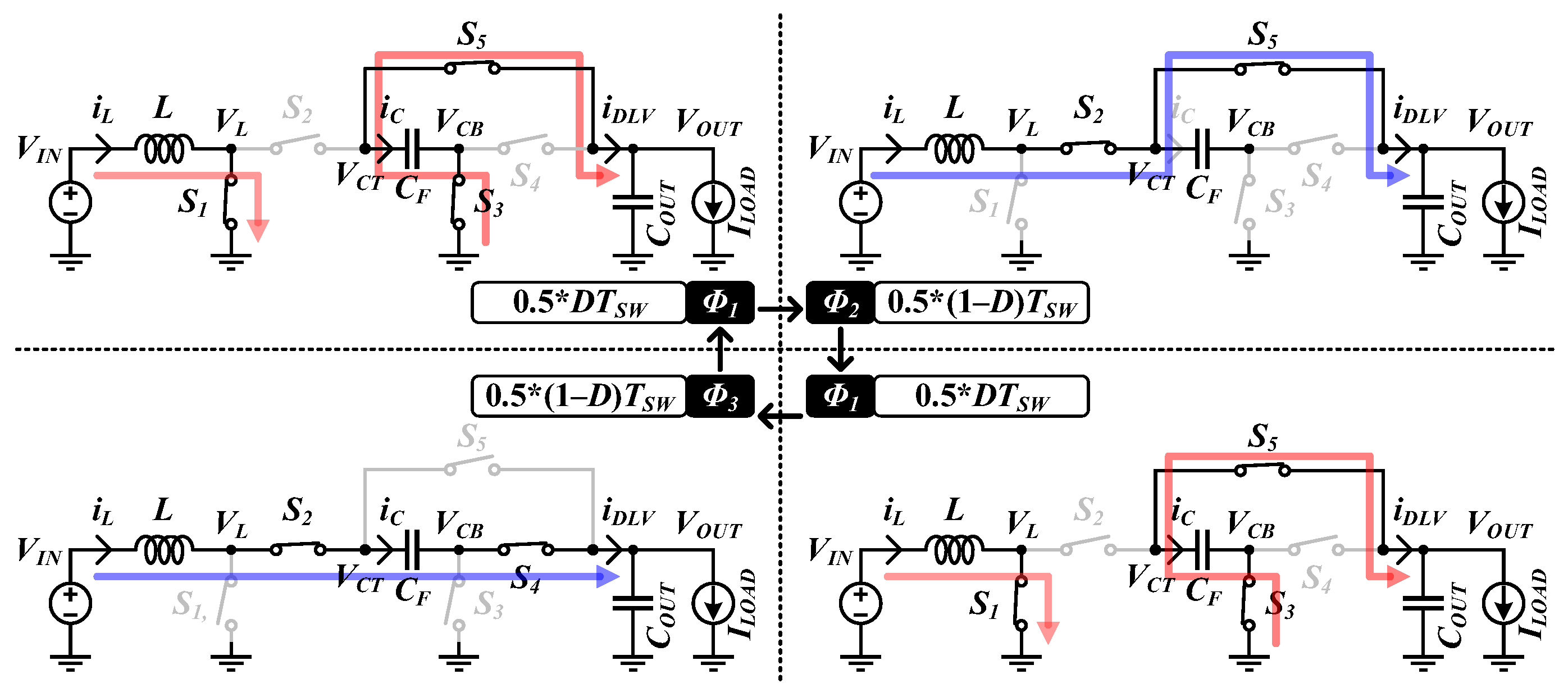
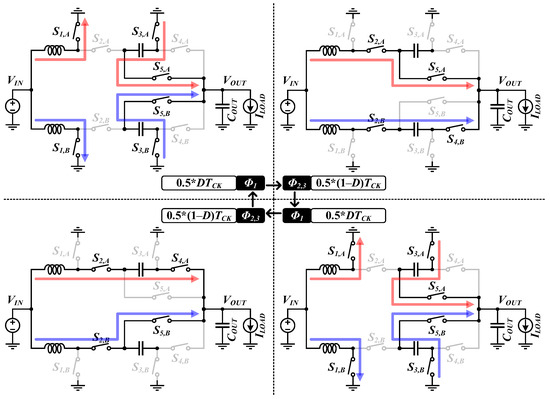
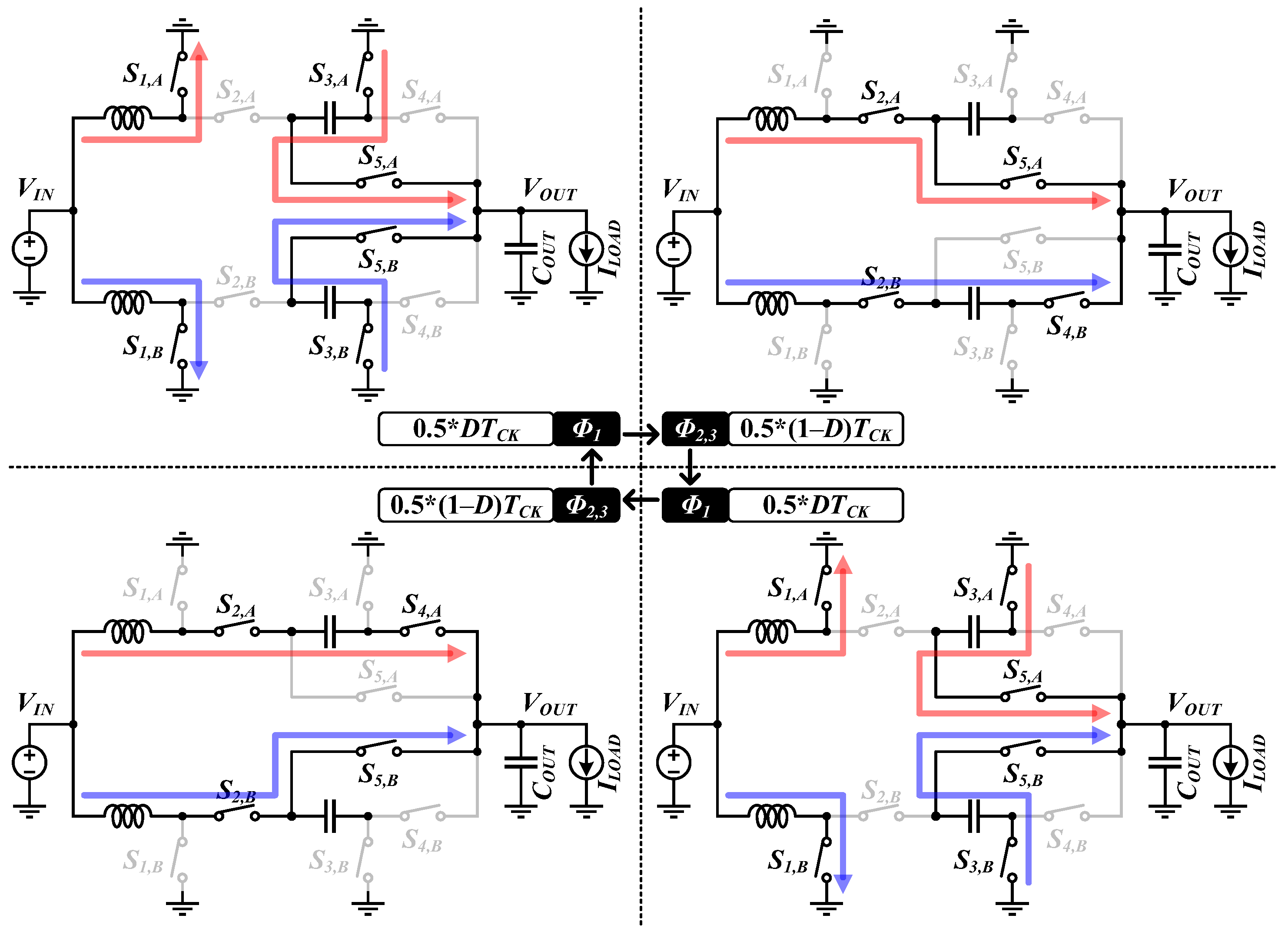
Figure 2 shows the proposed operation of a DPBB converter with a single stage. The conventional method in [7] has two operating phases with the same DPBB topology, as shown in Figure 1a. However, the proposed method operates in four phases, two of which are identical, as shown in Figure 2. Compared to prior converters, the proposed converter divides the duty cycle (D) by half and operates in two identical phases (Φ1).
Figure 2.
Proposed switching operation of the single-phase DPBB converter.
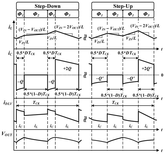
Figure 3 shows the waveforms of the proposed operation with a single power stage. As shown in Figure 2 and Figure 3, Φ1 is the first and third phases to charge iL via switch S1. During Φ1, iC flows to VOUT through charge sharing, and CF is discharged to VOUT. The second phase (Φ2) is the period during which the inductor is directly connected to VOUT. In this phase, only iL flows to VOUT. In this phase, the first node of the inductor is always connected to VIN, and the second node is connected to VOUT. Therefore, iL builds up when the power stage operates in the buck mode, and iL is discharged when it operates in the boost mode. After the second Φ1, the inductor and CF are connected in series during the last phase (Φ3), and current flows to the load. In this phase, iC is the same as −iL, and it satisfies the inductor volt-second rule.
Figure 3.
Waveforms of the proposed single-phase operation.
The conversion ratio of the proposed method (MPROP) is expressed by the volt-second rule on the inductor as follows:
where VIN denotes the input voltage of the DC–DC converter.
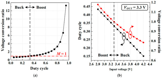
The proposed switching operation, in (2), has a conversion ratio of 2/3 to . Figure 4 shows the conversion ratio according to D. As shown in Figure 4a, the proposed converter operates as a buck converter when D is less than 1/3 and as a boost converter when D is greater than 1/3. As the proposed method is designed for Li-ion batteries, the target VIN ranges from 2.8 V to 4.2 V. Therefore, D of the proposed method ranges from 0.152 to 0.434 for the target VOUT of 3.3 V, as shown in Figure 4b. Prior hybrid buck–boost converters have mode-transition issues, in which the converters are controlled differently according to the operating modes. Therefore, complex control methods are required to achieve seamless mode transitions [1,2,3,4,9,11,13]. Most conventional works cannot cover the range of the conversion ratio to around unity. However, the operating mode of the proposed method is determined only by D, and MPROP ranges from 2/3 to without any missing regions.
Figure 4.
(a) Voltage conversion ratio curve according to the duty cycle, and (b) duty cycle according to VIN for VOUT = 3.3 V, where the black line represents the duty cycle and the red line represents the voltage conversion ratio.
2.2. Analysis of Conduction Loss
Many hybrid DC–DC converters have been designed to reduce the conduction loss by reducing the average value of iL (IL). Similarly, the proposed method utilizes a dual-path current design approach such that iC and iL flow to VOUT.
As shown in Figure 3, CF is discharged by iC during two Φ1s and charged by iL during Φ3. The charge balance of CF is expressed as follows:
In Φ3, the inductor and CF are connected in series, and the same current flows through them. Therefore, the charge that flows through CF during Φ3 is the same as the charge that simultaneously flows through the inductor, and it is expressed as follows:
Using (4), the average value of iC during Φ1 (IC,1) can be expressed as follows:
From the charge balance of the output capacitor (COUT), the relationship between IL and ILOAD can be derived as follows:
By substituting (6) into (8), IL can be expressed as
As shown in (9), IL of the proposed method in the buck mode is equal to the value that is reduced by the conversion ratio in ILOAD. In an inductive buck–boost converter, IIN and iDLV are discontinuous. Therefore, IL is always greater than ILOAD, and it causes large PCD, increased VOUT ripple, and higher switching noise. As ILOAD increases, these issues become more critical. However, the proposed work, including that of state-of-the-art hybrid DC–DC converters, solves the issue of the discontinuous iDLV and improves the power conversion efficiency.
When the converter operates under medium-to-heavy load conditions, the ripple component of the inductor current is relatively small compared to its DC component. Therefore, for analytical simplicity, the inductor current is approximated by its DC component when estimating conduction loss in the following analysis. To compare the effectiveness of the proposed operation, PCD of the proposed method (PCD,PROP) is analyzed as
where RON denotes the on-resistance of each power switch, and RDC denotes the DCR of the inductor. In this analysis, the RON of the power switches is assumed to be the same. By substituting (6) and (9) into (10), PCD,PROP can be expressed by ILOAD as follows:
Because the DC component of each current causes PCD, the ac current is ignored in this analysis. Table 1 presents a comparison of the characteristics of the proposed DPBB operation with those in prior works. As shown in Table 1, IL of the inductive buck–boost converter is always larger than ILOAD because the converter has discontinuous IIN and iDLV. However, the hybrid buck–boost converters, including the proposed work, have a continuous iDLV; therefore, they achieve a lower IL than ILOAD in the buck mode. The DC–DC converter in [9] has two different operating modes for the buck–boost converter, as shown in Figure 1b,c. Therefore, mode transition issues occur when VIN and VOUT become similar, and a complex control system is required to solve these issues. However, as mentioned previously, the proposed work has a single-mode operation, and therefore, it generates a target VOUT level even in a wide range of VIN through only duty control without the mode transition issues.
Table 1.
Comparison with prior buck-boost DC–DC converters.
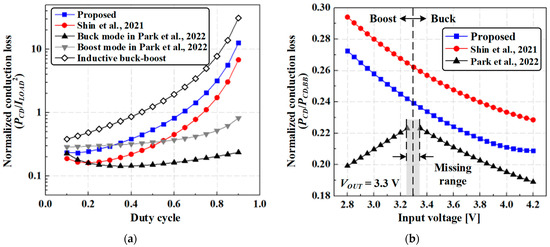
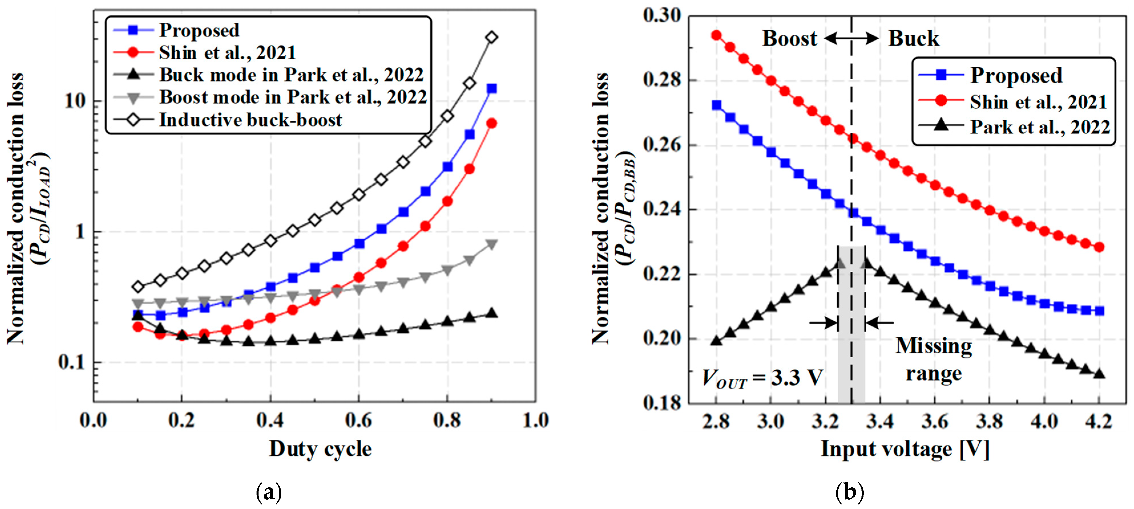
Figure 5 shows a comparison of the normalized PCD based on the analysis presented in Table 1. PCD as shown in Figure 5a is normalized by ILOAD2, and PCD as shown in Figure 5b is normalized by PCD of the inductive buck–boost converter (PCD,BB). As shown in Figure 5a, the proposed method always shows a lower PCD than that of the inductive buck–boost converter. In the inductive buck–boost converter, IL is always higher than ILOAD due to the discontinuous iDLV.
Figure 5.
Comparisons of the normalized conduction loss according to (a) the duty cycle and (b) input voltage, comparing the proposed work with those in [7,9].
For a fair comparison with state-of-the-art works, PCD is compared by considering the operating conditions of Li-ion batteries. The target VIN ranges from 2.8 V to 4.2 V, and the target VOUT is 3.3 V for mobile applications. Figure 5b shows a comparison of PCD,PROP to each PCD of the prior works under the operating conditions such that their respective VIN, VOUT, and clock frequency (fCK) are the same. As shown in Figure 5b, the proposed method shows a lower PCD than that of the converter in [7]. The longer the period of DTCK, the higher the PCD, because IL increases with D. For the same VOUT level, D of the proposed method is always lower than that in [7]. This implies that the proposed method always has a lower IL than the prior method, and therefore, the proposed method shows lower PCD even with the same power stage topology.
In the case of the boost mode, the proposed method and the method in [7] have a larger IL than ILOAD because the inductor is always connected to VIN. Therefore, IL increases as the conversion ratio increases. However, the hybrid buck–boost converter in [9] always has a lower IL than ILOAD because it utilizes the switched-inductor-capacitor topology and dual-path current technique in the boost and buck modes, respectively. Moreover, the number of power switches in the current path is smaller than that in the proposed method. Although the converter in [9] shows lower PCD, the difference in power loss decreases when VIN approaches 3.3 V. In addition, regulating VOUT becomes difficult because of the missing conversion-ratio range.
2.3. Analysis of Inductor Current Ripple
One advantage of the proposed method is its low iL ripple. As shown in Figure 3, the iL ripple of the proposed method can be expressed as follows:
where ∆iL denotes the ripple of iL. Using (2), D is expressed by MPROP to compare the ripple of iL according to the conversion ratio. Subsequently, iL can be expressed as follows:
The iL ripple of the prior converters is also analyzed according to the conversion ratio, as shown in Table 1. As mentioned previously, the converter in [7] comprises the same power stage as that in the proposed work, but it operates only in two phases (Φ1 and Φ3). It always builds up iL with the voltage across the inductor of VIN, and discharges with (VIN − 2VOUT). However, the proposed method operates in three phases, and whether iL is charged or discharged during Φ2 is determined by the operating mode. Unlike Φ3, a voltage of (VIN − VOUT) is applied across the inductor in Φ2. Therefore, as shown in Figure 3, iL builds up more in the buck mode and is discharged in the boost mode during Φ2. In this case, the inductor voltage during Φ2 is lower than that during Φ3, and this makes the ripple of iL 33.33% smaller than that in the conventional work.
With respect to the conversion ratio, the two-phase operation regulates VOUT down to a low voltage close to 1/2 of VIN, but the proposed method regulates down to 2/3 of VIN for low iL ripple. When considering the applications of Li-ion batteries, the conversion ratio of (2/3 < MPROP < ) is sufficient for VOUT to reach the target voltage of 3.3 V.
iDLV of the DPBB topology comprises iL and iC,1. In the capacitor-delivery phase, the iDLV is determined by the charge-sharing process between capacitors, which results in an exponential current profile. Compared with the linearly varying inductor current, this behavior produces a larger instantaneous variation in the delivered current, leading to increased iDLV ripple. To analyze this behavior, the capacitor current iC,1 during the charge-sharing process can be expressed as
where τ is the time constant composed of both resistance and capacitance including CF. The charge balance of the CF defines the coefficient I0 of (16). In other words, both the average values of iC,1 and iL,3, which is the L-path current in Φ3, should be the same in steady state, which is expressed as follows:
Substituting (17) into (16), iC,1 is given by
From (18), the ic,1,pp (peak-to-peak iC,1) can be expressed as
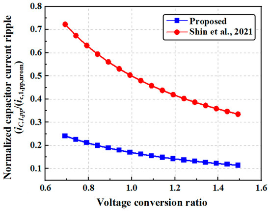
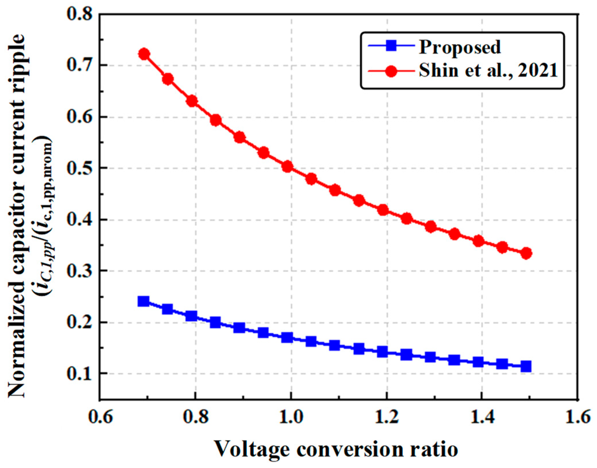
Figure 6 compares the capacitor current ripple of the proposed structure and that of [7]. Here, ic,1,pp,norm denotes the normalized capacitor current ripple, defined as ILTCK/τ. As shown in Figure 6, the proposed structure exhibits a smaller capacitor current ripple than [7] over the entire buck–boost conversion-ratio range.
Figure 6.
Comparisons of the normalized capacitor current ripple, comparing the proposed work with that in [7].
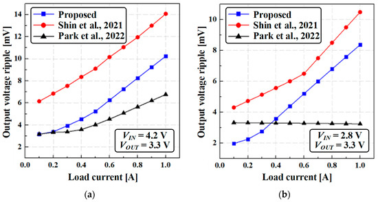
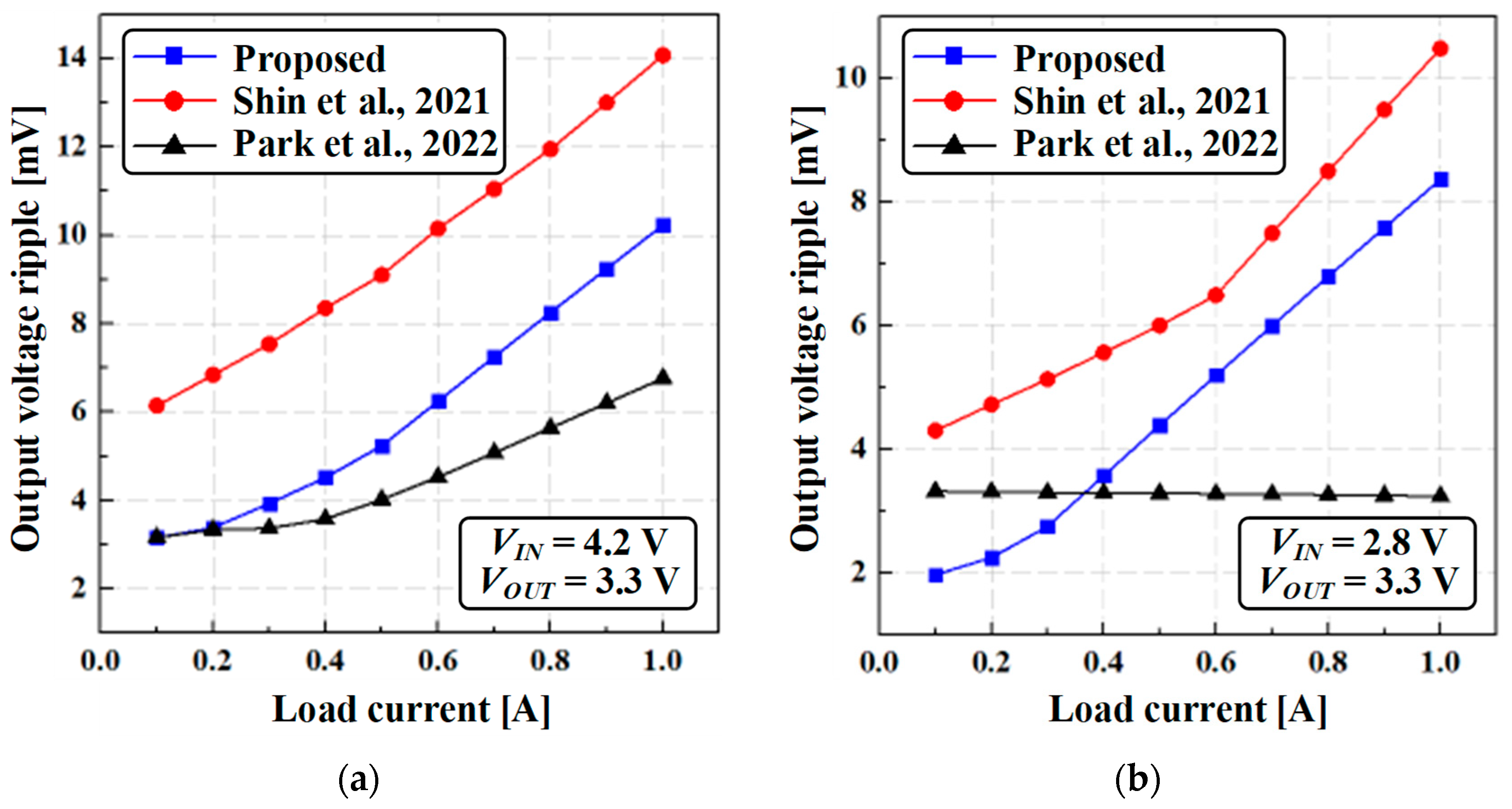
Figure 7 shows the simulation results of the VOUT ripple according to ILOAD in the buck and boost modes. As shown in Figure 7a, the VOUT ripple increases as ILOAD increases in all the cases.
Figure 7.
Comparisons of the output voltage ripple between the proposed work and conventional works in [7,9]: (a) buck mode and (b) boost mode.
In the case of the converter in [9], iL is always delivered to VOUT, and it utilizes a longer D than the others. Therefore, the VOUT ripple is smaller than that in other works. When compared to the operation in [7], the proposed method shows a smaller ripple of VOUT because it has a smaller capacitor current ripple, as discussed in Figure 6. In the case of the boost mode, the method in [9] shows the smallest ripple of VOUT since iDLV is equal to iL, as shown in Figure 7b. When compared to the prior DPBB converter, the proposed method also shows a smaller VOUT ripple.
3. Circuit Implementation
3.1. Dual-Phase Dual-Path Buck-Boost Converter
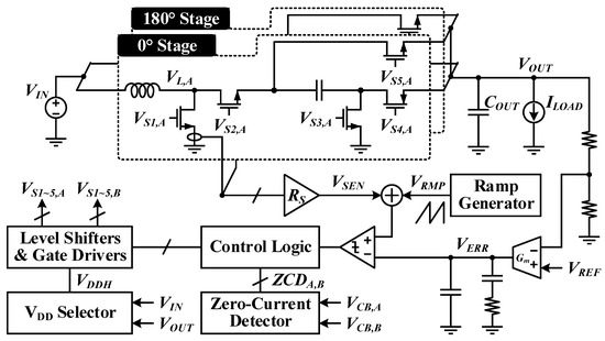
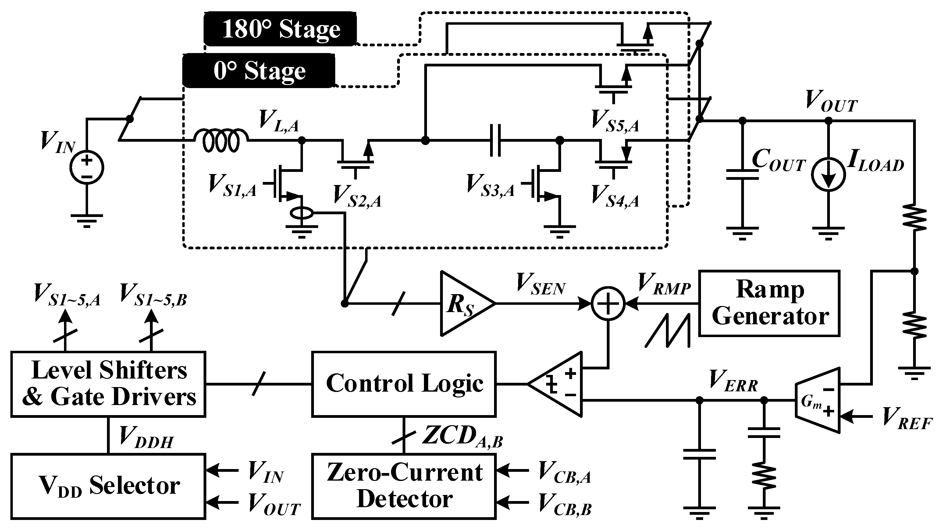
Figure 8 shows the top block diagram of the proposed hybrid dual-phase DPBB converter. It has two DPBB stages which operate with a phase difference of 180°. D is determined by the error voltage (VERR) and ramp signal, which is compensated by the current sensor [27] for low-sided power switches. The proposed work adopts a dual-phase structure with 2.2 μH commercially available shielded ferrite-core inductors (Bourns, Riverside, CA, USA). Due to the low power level and limited flux swing, the magnetic core loss is negligible compared to conduction and switching losses at 1 MHz. In addition, the proposed offset-controlled ZCD is implemented to enhance efficiency under light-load conditions. The level shifters and inverter-based drivers employ a VDD selector to drive the power switches.
Figure 8.
Top block diagram of the proposed dual-phase DPBB converter.
Figure 9 shows the four-phase operation of the proposed dual-phase DPBB converter. Both DPBB stages build each iL up during Φ1. From Φ1 to half of the clock cycle, the first power stage operates at Φ2, and the second stage operates at Φ3 such that each iL is discharged. Subsequently, the iL-charging phase is repeated for half the duty cycle. The first and second power stages operate at Φ3 and Φ2, respectively.
Figure 9.
Operation of the proposed dual-phase DPBB converter.
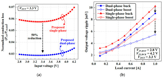
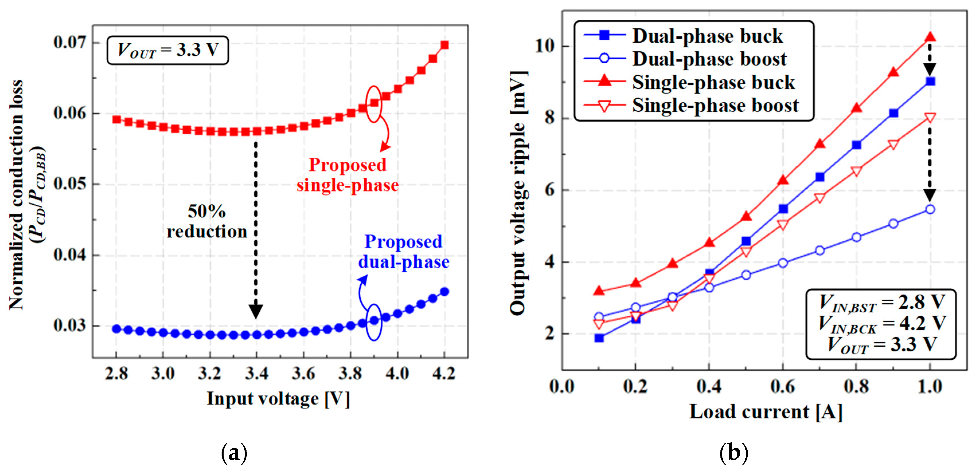
The proposed converter employs a dual-phase power stage, reducing the average inductor current to half of that in a single-phase DC–DC converter. Accordingly, the total conduction loss due to DCR is reduced by approximately 50%, as shown in Figure 10a. In addition, the 180° interleaved operation mitigates the output ripple through partial ripple cancellation. The phase-shifted inductor currents reduce the AC component at the output, resulting in a smaller VOUT ripple. Figure 10 presents the performance comparison between single- and dual-phase DPBB converters. As shown in Figure 10b, the dual-phase operation achieves a VOUT ripple reduction of up to 2.567 mV (67.5%).
Figure 10.
Comparison of the (a) conduction loss and (b) output voltage ripple.
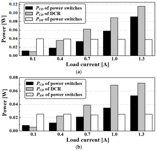
Figure 11 shows the simulated loss breakdown of the proposed dual-phase DPBB converter according to ILOAD with different input voltages. PSW includes both the voltage-current overlap loss during switching transitions and the gate chargimg and discharging loss. Figure 11a shows the loss breakdown with VIN = 2.8 V. When compared to that with VIN = 4.2 V, it shows a larger PCD with the same ILOAD because the conductivity of the power switches is less with lower supply voltage. Under the light-load condition of ILOAD = 100 mA, the total loss is calculated as an average of 15.09% of the output power. At ILOAD = 1.3 A, the portion of the power loss is reduced in efficiency, and the total loss is calculated as 4.423% of the output power on average.
Figure 11.
Loss breakdown of the proposed dual-phase DPBB converter according to ILOAD at (a) VIN = 2.8 V and (b) VIN = 4.2 V.
3.2. Proposed Offset-Controlled Zero-Current Detector
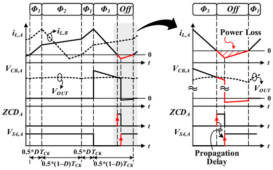
As mentioned previously, the proposed dual-phase hybrid buck–boost converter operates in DCM over a wider ILOAD range than single-phase converters. In conventional implementations, ZCD is typically performed using a single static comparator that compares the relevant node voltages. Figure 12 shows the waveforms of DCM operation with the conventional static comparator. As shown in Figure 12, although the static comparator ideally detects the zero-current point when VCB equals VOUT, its propagation delay causes the power switches (S4,A and S4,B) to turn off after iL reaches 0 A. Consequently, reverse inductor current flows, leading to additional power loss.
Figure 12.
Waveforms of the proposed dual-phase DPBB converter with the strong-armed-latch comparator in DCM.
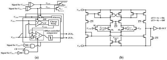
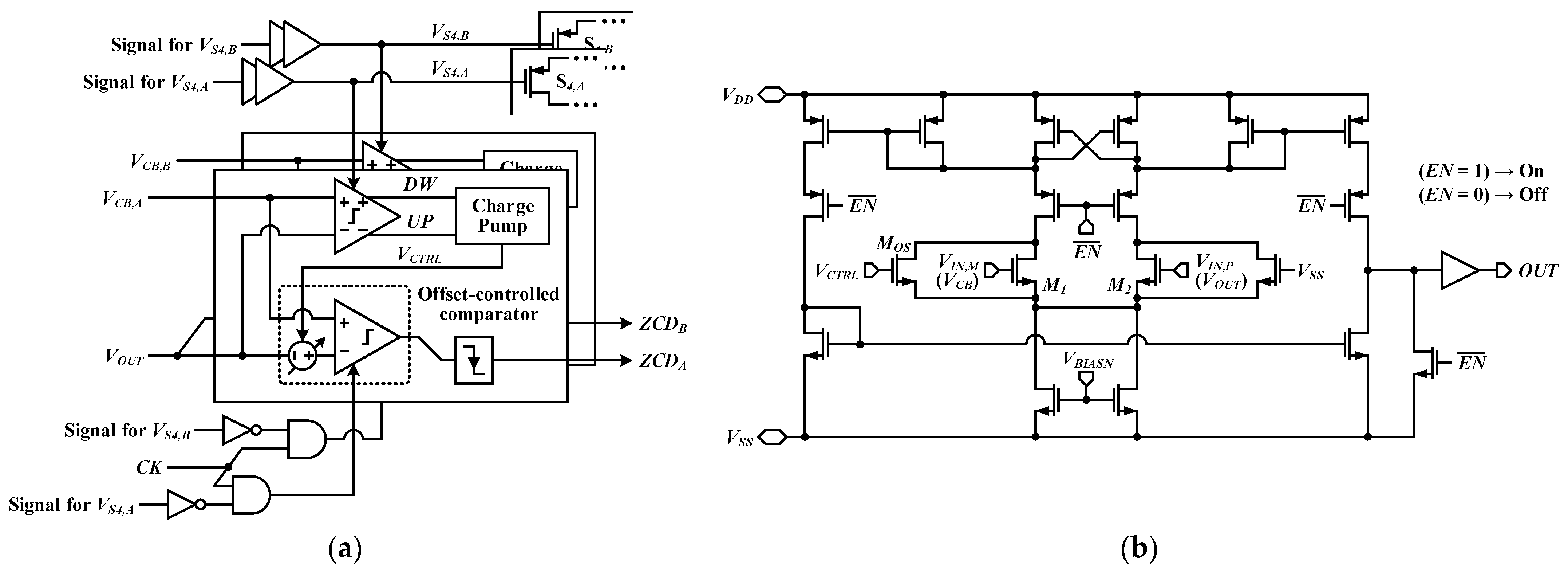
To compensate for the timing mismatch owing to the propagation delay, an offset-controlled ZCD is proposed. The block diagram is shown in Figure 13a, and it consists of an offset-controlled comparator, a charge pump, and a dynamic comparator. A schematic of the offset-controlled strong-arm latch comparator for the proposed ZCD is shown in Figure 13b. It is designed with the duty-cycled type to reduce power consumption [28]. When input voltage (VCB) falls below the negative input voltage (VOUT), an intentional offset voltage (VOS) is introduced at the negative input transistor (M1) by connecting an offset-injecting transistor (MOS) in parallel. For the analytical derivation, both M1 and MOS are assumed to operate in the saturation region, and the large-signal MOS drain current equation is used. The resulting VOS is calculated as follows:
where VCTRL denotes the control voltage of MOS.
Figure 13.
Block diagram of the proposed (a) offset-controlled ZCD, and (b) offset-controlled strong-arm latch comparator.
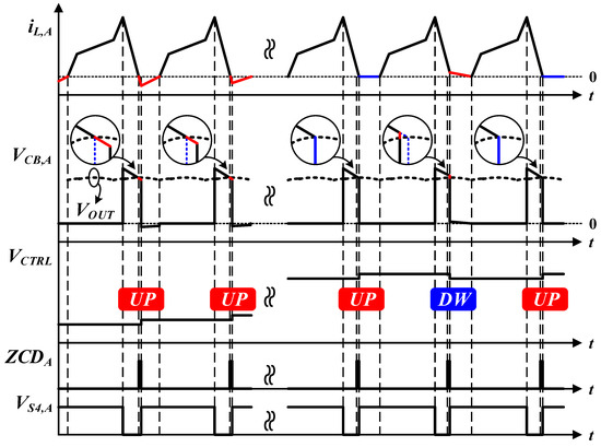
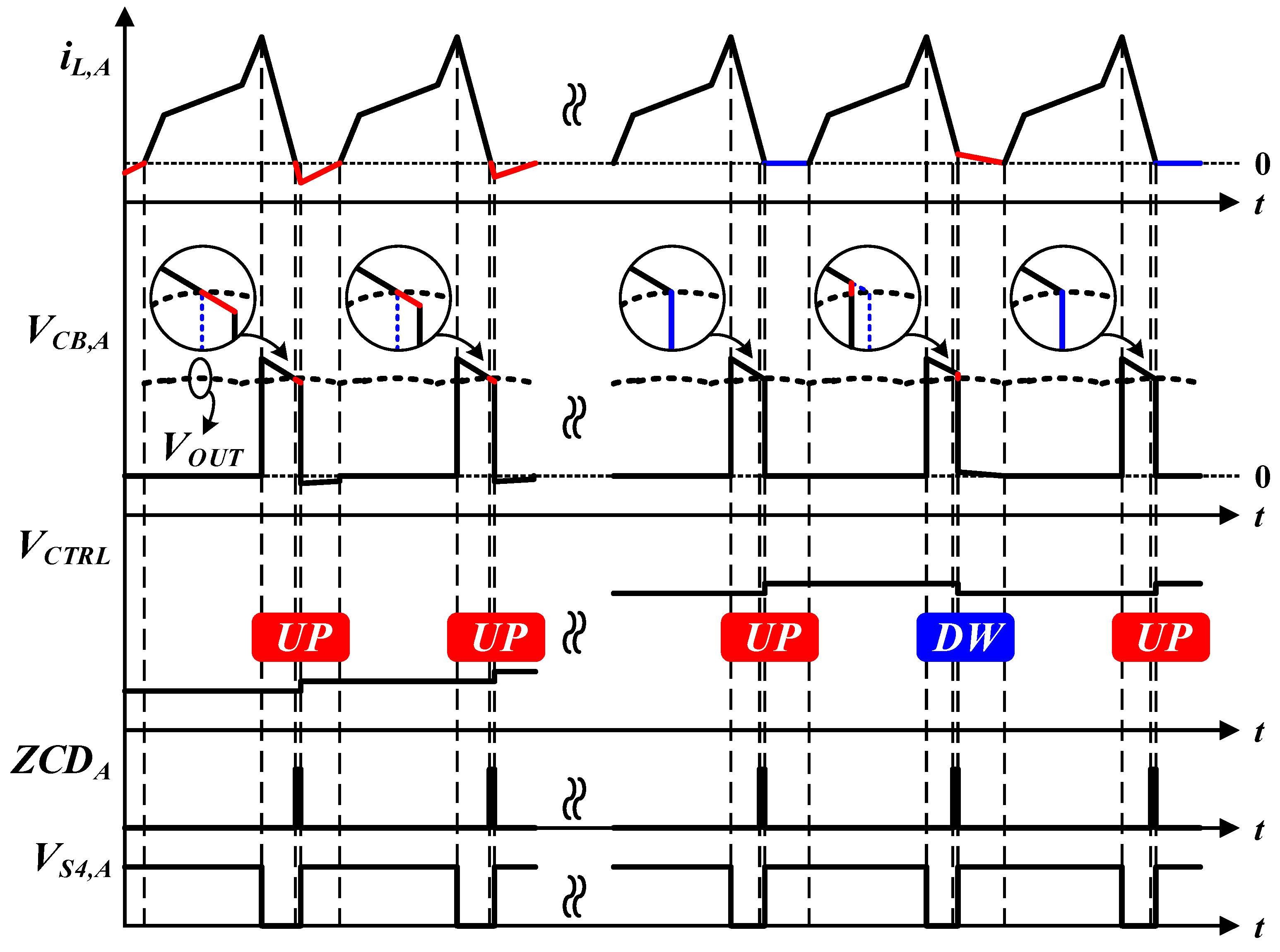
Figure 14 shows the waveforms of the proposed ZCD. When the buffered gate signals (VS4,A and VS4,B) are triggered to turn off the power switches, the dynamic comparator determines whether VCB or VOUT is higher. If VCB is lower than VOUT, the charge pump increases the offset voltage (VCTRL), and the output signals of the offset-controlled ZCD (ZCDA and ZCDB) are triggered earlier. Otherwise, if VCTRL is higher than the optimum point, S4,A and S4,B are turned off when VCB is higher than VOUT. This implies that the power switches are turned off when each iL is still positive, and that some charge remains to be transferred to VOUT. Therefore, the charge pump decreases VCTRL to reduce the offset voltage of the proposed ZCD, as shown in Figure 14.
Figure 14.
Waveforms of the proposed offset-controlled ZCD.
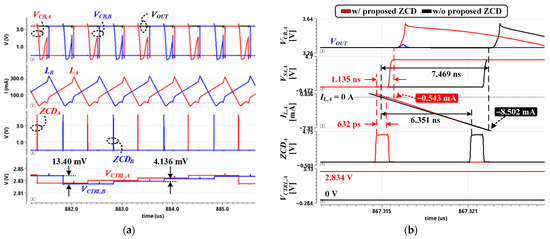
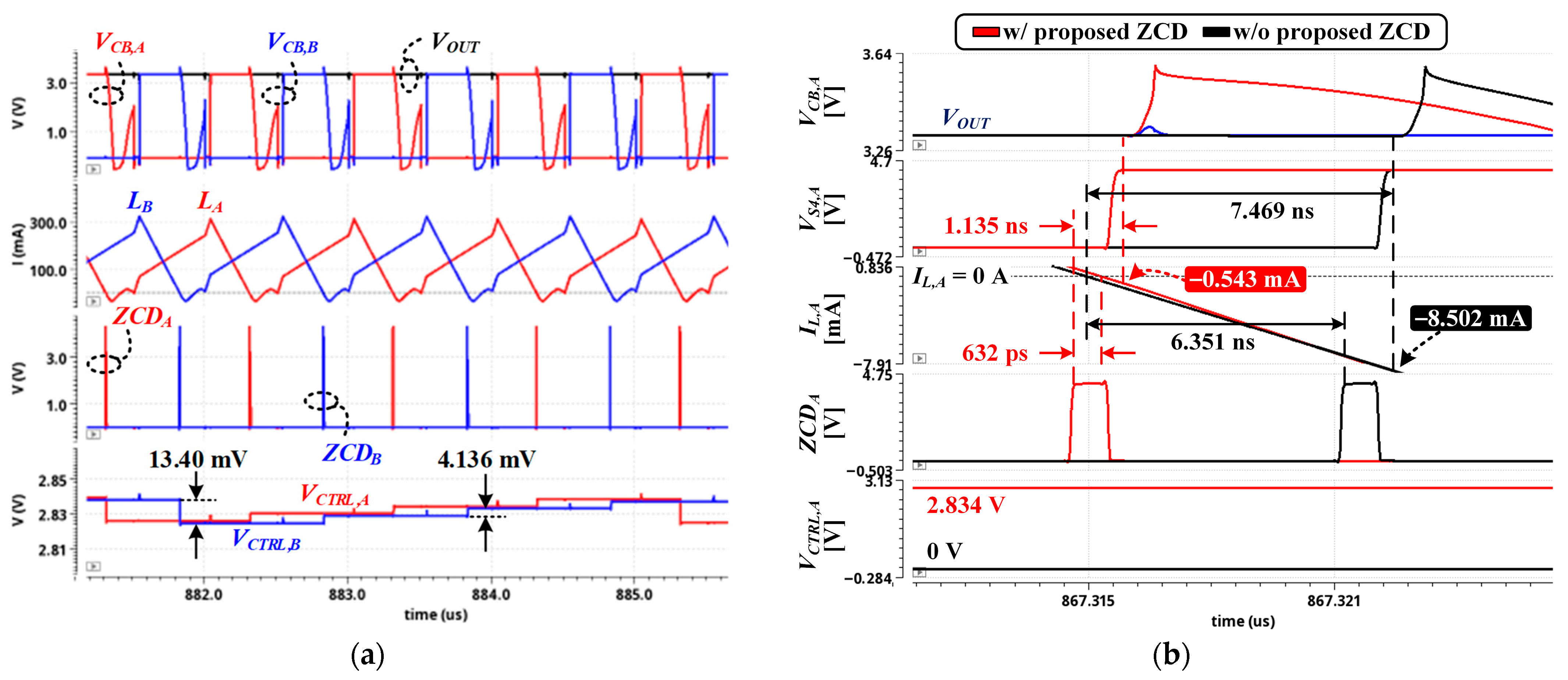
Figure 15 shows the simulation results of the proposed ZCD. With 3.3 V of VOUT, each VCTRL is regulated at 2.833 V on average. Figure 15b compares the accuracy of the proposed ZCD with the conventional work, which comprises the strong-arm-latch comparator. The conventional work suffers from both propagation delay and comparison time; therefore, the power switches are turned off at IL,A of −8.502 mA. However, the proposed ZCD turns off the power switch at −0.543 mA of IL,A by intentionally applying and adjusting the offset to the comparator.
Figure 15.
Simulation results of (a) the steady-state operation of the proposed ZCD and (b) comparison to the conventional work.
The bias-control ZCD forms a bang-bang feedback loop that iteratively adjusts the comparator offset. Since the resulting timing correction step is much smaller than the comparator decision time, the loop converges stably without oscillation.
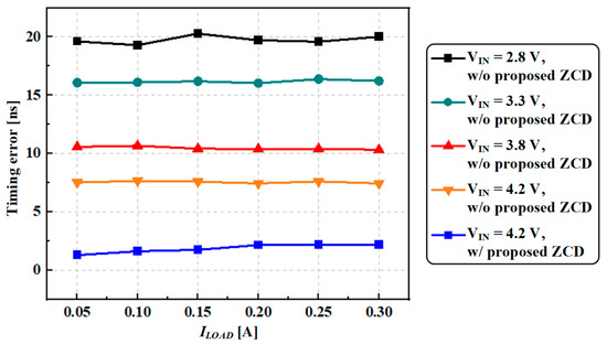
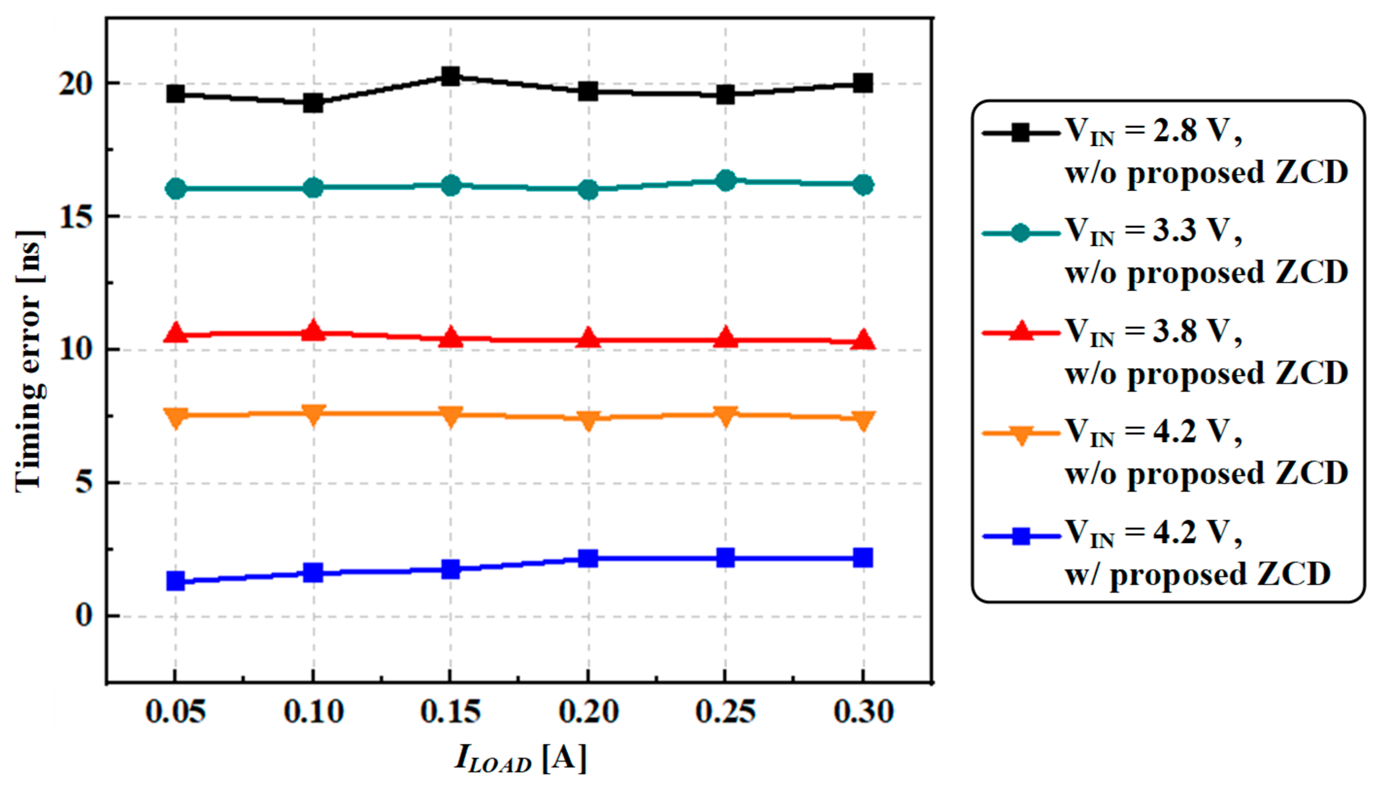
Figure 16 shows the simulation results of the timing error according to ILOAD. As the input voltage decreases, the bandwidth of the comparator used in the ZCD decreases, which degrades timing error. In addition, the propagation delay of the logic and driver also increases as the input voltage decreases, resulting in a larger timing error. On the other hand, the slope of the inductor current is determined by the voltage difference across the inductor. Therefore, the decreasing slope of the inductor current is only weakly affected by ILOAD. As a result, for a fixed VIN, the variation in timing error with respect to ILOAD is relatively small.
Figure 16.
Comparison of timing error with and without the proposed ZCD.
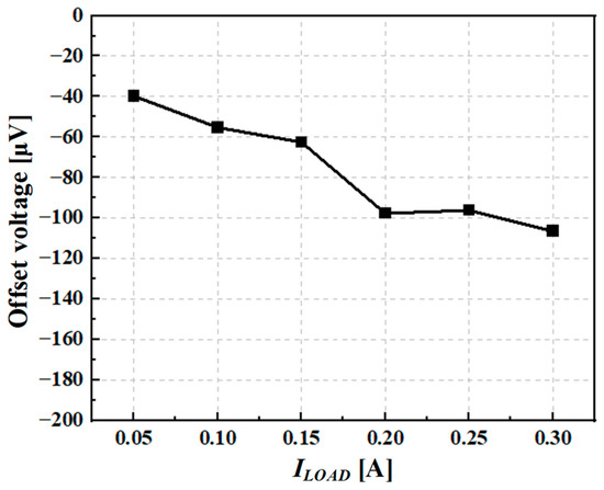
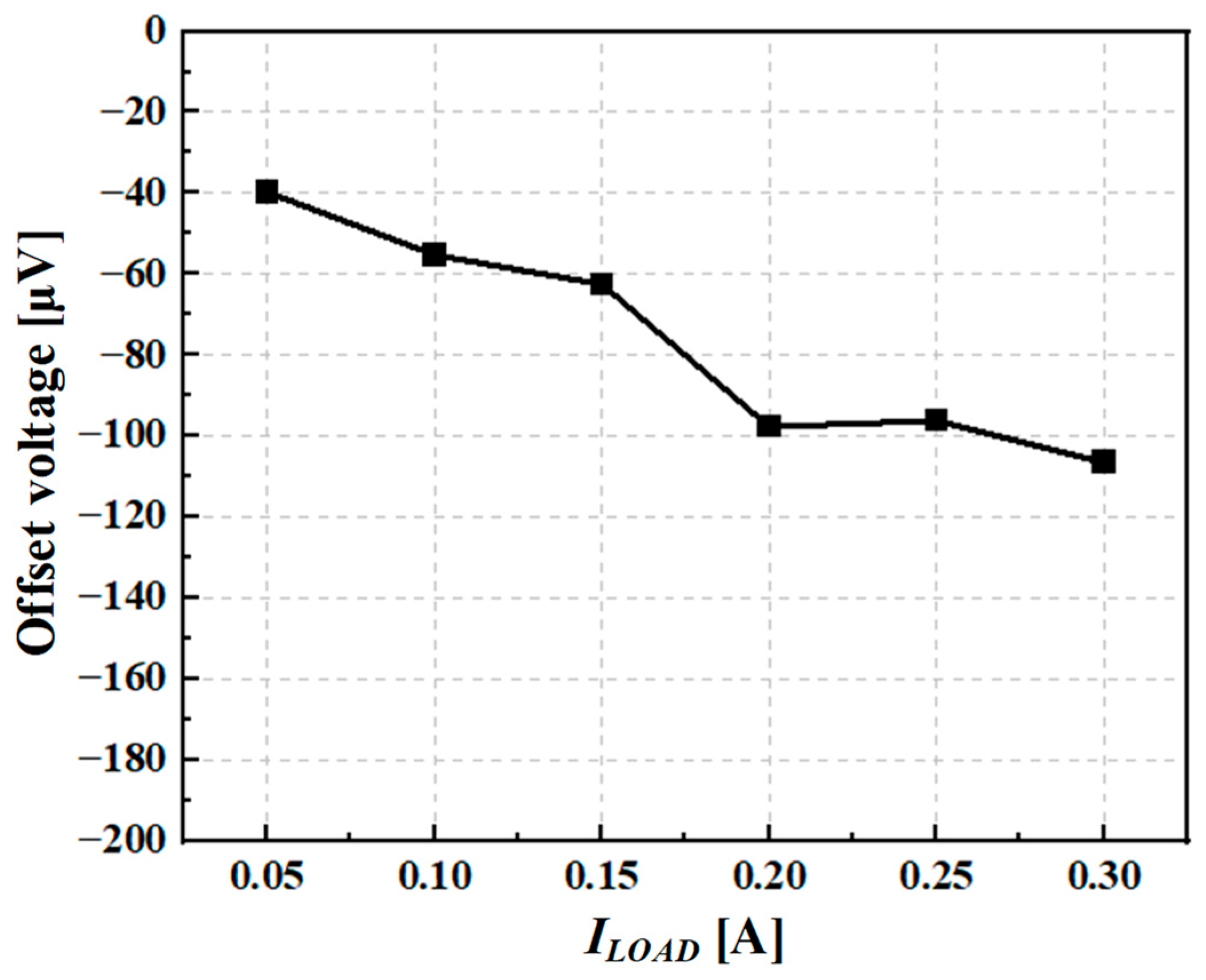
Figure 17 shows the relationship between the required comparator offset VOS and the load current. As the load current increases, the magnitude of the required offset increases from approximately −40 μV to −100 μV. This is because the slope of VCB becomes steeper near the zero-crossing point as the load current increases. As a result, a larger offset is required to compensate for the ZCD sensing delay and to suppress reverse inductor current.
Figure 17.
Variation of the comparator offset voltage with load current.
4. Measurement Results
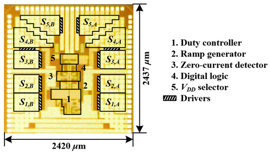
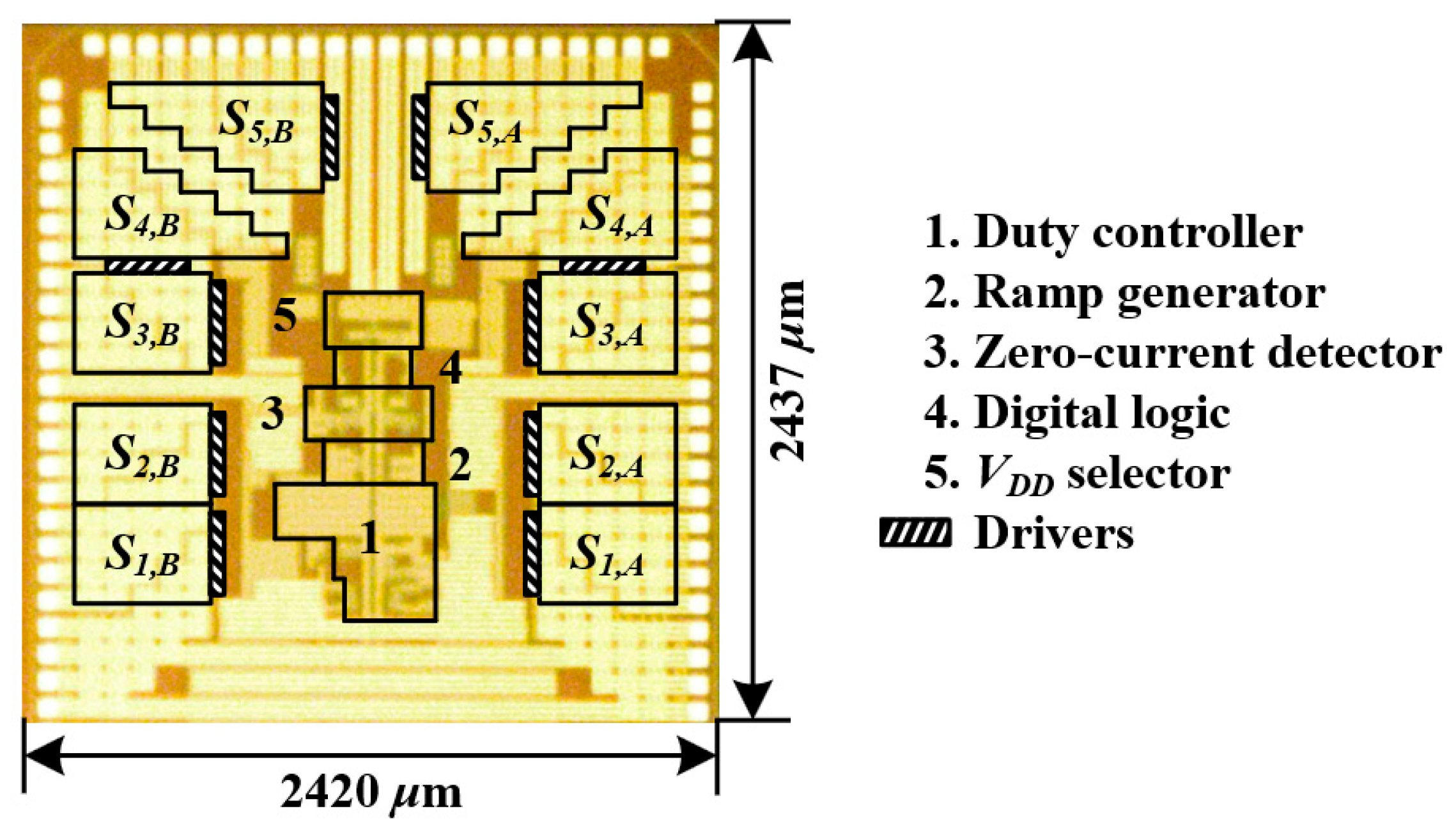
Figure 18 shows a chip micrograph of the proposed dual-phase DPBB converter. The chip is fabricated using a 1P6M 180-nm BCD process for performance verification. The chip area is 5.897 mm2 and the core area is 3.82 mm2. Two inductors of 2.2 μH (DCR = 140 mΩ) are used, and the size of both CF and COUT is 10 μF. The switching period of the system is designed to be 1 MHz. VOUT is regulated to 3.3 V, and the chip is measured while changing VIN and ILOAD.
Figure 18.
Chip micrograph.
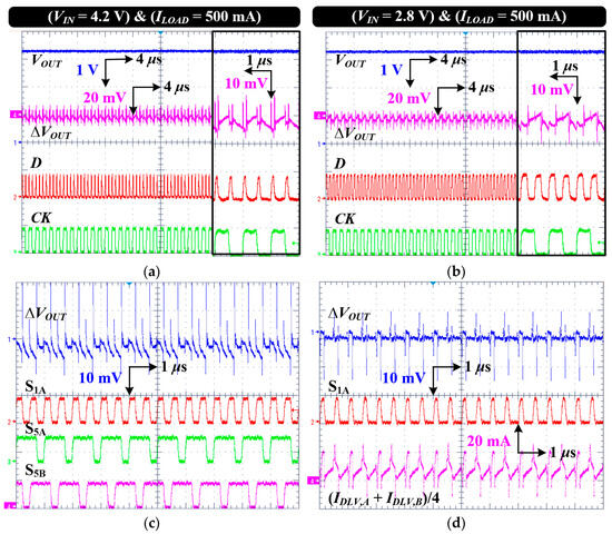
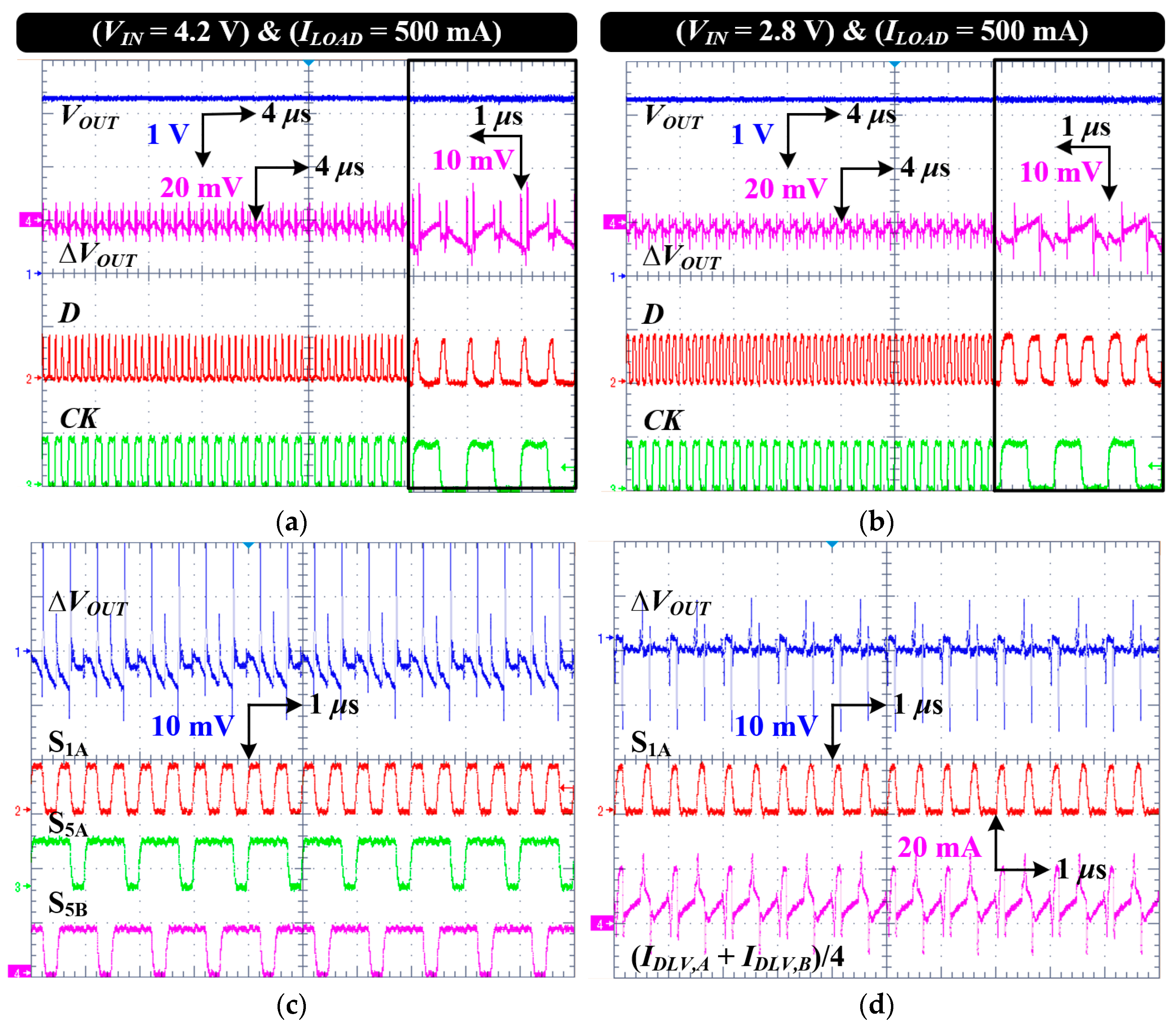
Figure 19a shows the measured waveforms of the buck mode at VIN = 4.2 V and ILOAD = 500 mA. The ripple of VOUT is measured as 8 mV, excluding the switching noise owing to the equivalent series resistance of COUT. Figure 19b shows the steady-state waveforms of the boost mode at VIN = 2.8 V and ILOAD = 500 mA. In this case, the VOUT ripple is measured as approximately 7 mV. Because iDLV of the proposed work is always continuous with alternative iL and iC, the VOUT ripple is reduced under the similar operating conditions when compared to that of the conventional works [5,9]. Figure 19c shows the ripple of VOUT and gate signals with D = 0.43. Figure 19d shows the total iDLV with the ripple of VOUT. The waveform of the total iDLV corresponds to 25% of the actual iDLV under the light-load condition.
Figure 19.
Measured steady-state waveforms: (a) buck mode at VIN = 4.2 V and ILOAD = 500 mA; (b) boost mode at VIN = 2.8 V and ILOAD = 500 mA; (c) VOUT ripple and gate signals at D = 0.43; (d) total iDLV with the VOUT ripple.
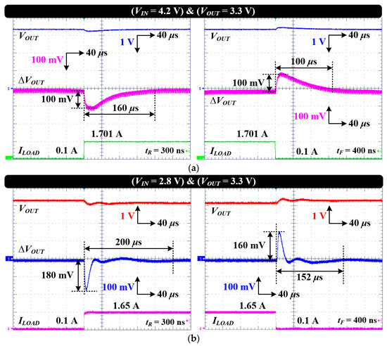
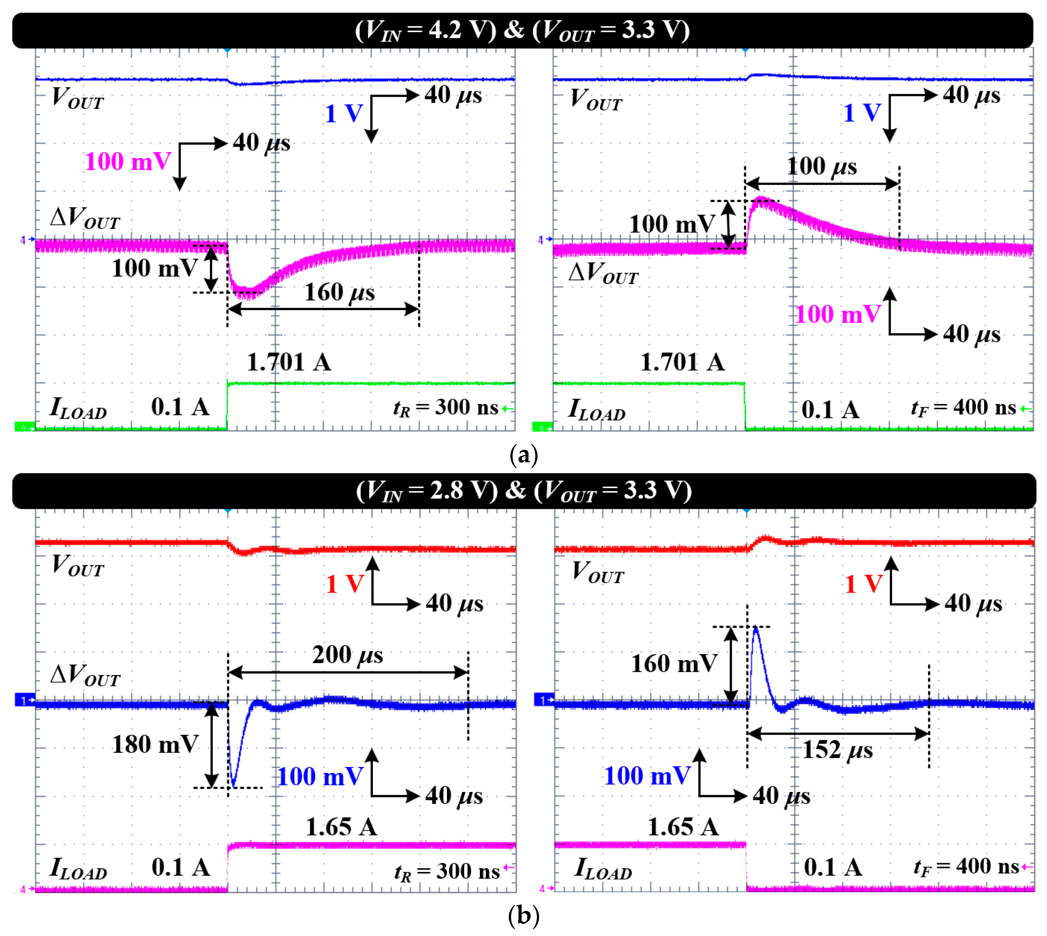
Figure 20 shows the load-transient response of the proposed work. As shown in Figure 20a, ILOAD is changed between 0.1 A and 1.701 A with VIN = 4.2 V. The undershoot of VOUT is measured to be approximately 100 mV, and the settling time is measured to be 160 μs. The overshoot is measured at approximately 100 mV with a settling time of 100 μs. Figure 20b shows the load-transient response with VIN = 2.8 V. As VIN decreases, the overall response deteriorates for similar ILOAD change. The topology in this work stores the energy in the inductor during D, and this delays the energy transfer the input to VOUT under light-to-heavy load transition. Therefore, it has a right-half-plane zero due to indirect energy transfer.
Figure 20.
Measurement load-transient response with (a) VIN = 4.2 V and (b) VIN = 2.8 V.
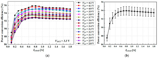
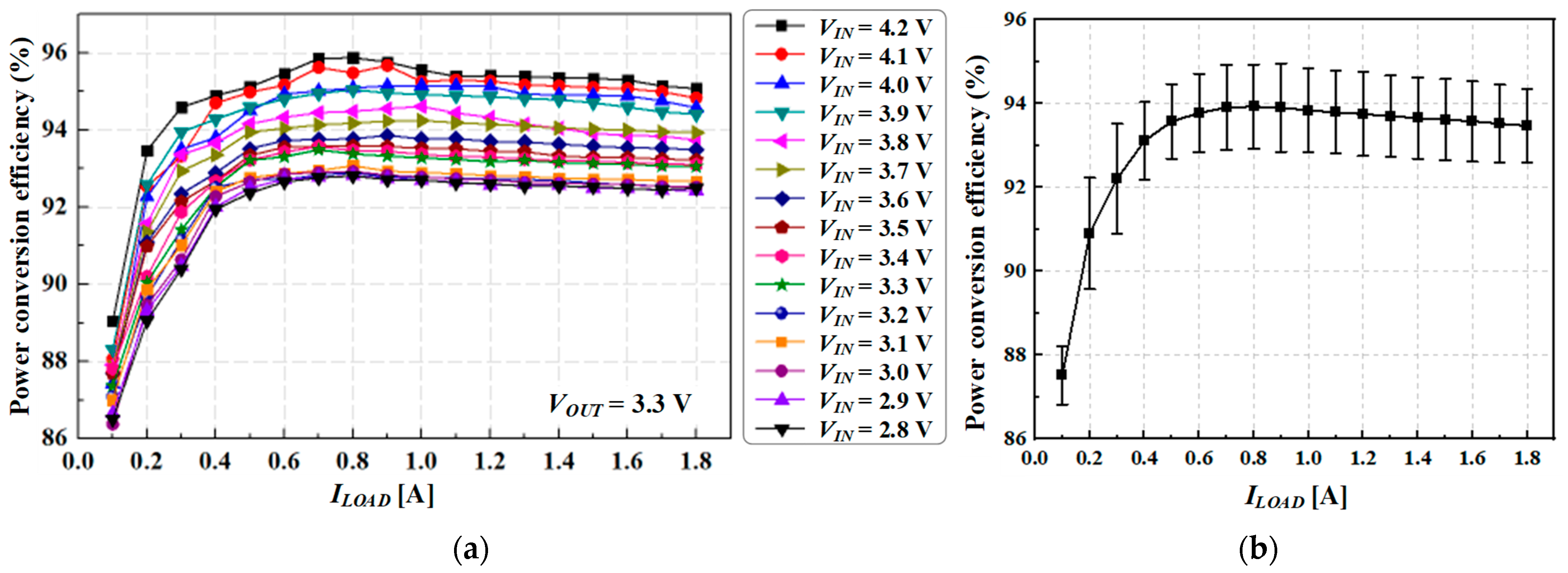
The measured power conversion efficiency of the proposed work is shown in Figure 21. The efficiency is measured VIN ranging from 2.8 V to 4.2 V for the Li-ion battery applications. The peak efficiency in the boost mode is measured to be 95.88% at VIN = 4.2 V and ILOAD = 800 mA. The peak efficiency in the buck mode is measured to be 93.08% at VIN = 3.1 V and ILOAD = 800 mA. The proposed work is designed to a higher ILOAD range exceeding 1 A; therefore, the sizes of the power switches are designed to be larger than those of certain prior hybrid buck–boost converters. As shown in Figure 21, the lower the VIN, the lower the conductivity of the power switches, and consequently, the lower the efficiency. When VIN decreases by 100 mV, the power conversion efficiency decreases by approximately 2.1%. However, the proposed hybrid buck–boost converter maintains more than 90% efficiency for ILOAD larger than 300 mA over all VIN ranges.
Figure 21.
Measurement power conversion efficiency curves: (a) PCE versus ILOAD for different VIN; (b) PCE with error bars.
Figure 21b shows the average efficiency with error bars derived from the results in Figure 21a. The error bars represent the standard deviation of the efficiency obtained under different input voltage conditions. The standard deviation remains around ~1% and reaches a maximum of approximately 1.3% across the load range. This result indicates that the efficiency variation with respect to the input voltage is relatively small, demonstrating that the proposed converter maintains stable efficiency over the wide input voltage range.
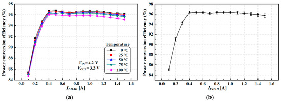
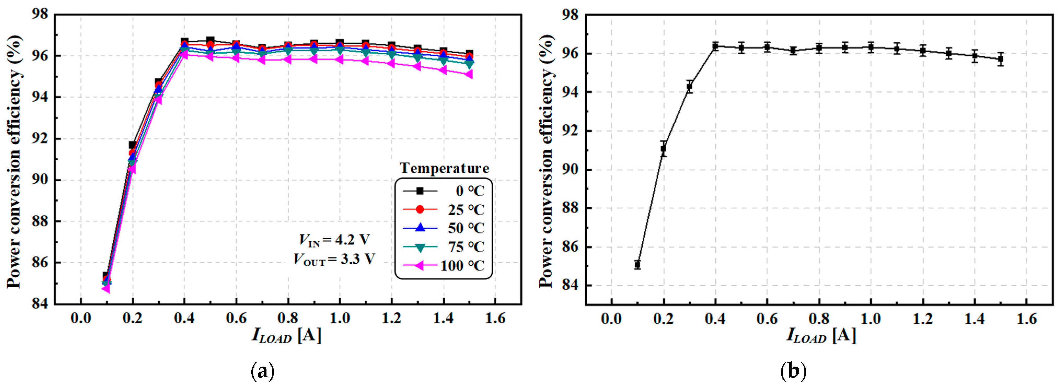
By comparing the measured PCE (power conversion efficiency) and the post-layout simulation results at room temperature (25 °C), the two results exhibit a similar trend. Although a larger deviation appears in the light-load region, the difference is around 1% in the normal load region. Based on this observation, the temperature-dependent PCE characteristics from 0 °C to 100 °C are analyzed through post-layout simulation in this work.
Figure 22 shows the temperature-dependent power conversion efficiency characteristics of the proposed converter. Figure 22a illustrates the PCE curves with respect to load current at five different temperatures. As the temperature increases, the PCE slightly changes due to the temperature-dependent characteristics of the power devices and passive components. Figure 22b presents the average PCE with error bars derived from the results in Figure 22a. The error bars indicate the standard deviation of the PCE across the different temperature conditions, while the solid line represents the mean value.
Figure 22.
Simulation results of temperature-dependent power conversion efficiency curves: (a) PCE versus ILOAD for different temperature; (b) PCE with error bars.
Table 2 presents a performance summary of the proposed work with a comparison to the state-of-the-art hybrid buck–boost converters. When compared to that in [7], the proposed work is designed with the same topology as that of the power stage. However, the proposed work is configured with dual phases to drive a wider range of ILOAD. As a result, smaller iL ripples and VOUT ripples are obtained with four operating phases per cycle. In addition, several hybrid buck–boost converters reported in [29,30,31] are included in Table 2 to provide a broader performance comparison. The comparison results indicate that the proposed work achieves competitive efficiency compared with the prior works.
Table 2.
Performance comparison with prior hybrid buck-boost converters.
Furthermore, the load-transient response of the proposed structure is compared with the prior work in [7]. The proposed structure is capable of delivering a significantly larger load current. Specifically, the proposed structure achieves a current density of 0.68 A/mm2, which is higher than 0.32 A/mm2 reported in [7], indicating a stronger load driving capability per unit area. In terms of load-transient performance, the proposed structure also demonstrates competitive dynamic characteristics. The proposed structure achieves a TSETTLE (settling time) of 160 μs for a load step of 1.6 A, whereas [7] reports a TSETTLE of 150 μs for a load step of 0.45 A. When compared with the converters in [29,30,31], the proposed converter also demonstrates higher current density, implying improved load driving capability per unit chip area. Despite experiencing approximately more than three times larger load step, the proposed structure maintains a comparable TSETTLE to that of [7]. These results verify that the proposed structure provides fast and stable load-transient response even under large load current variations.
The prior hybrid buck–boost converters require more than two operating modes for the buck and the boost modes. However, the proposed work has only one switching operation, and the operating mode is determined by only D to address the mode transition issues. Most hybrid buck–boost converters have a continuous iDLV, but IIN is not continuous. Therefore, they have a dip in the power efficiency with the bondwire parasitic inductance [32]. However, both IIN and iDLV of the proposed work are continuous; therefore, the input capacitor could be smaller than in the prior works. Moreover, as the average iL level is reduced with the dual-path strategy, the efficiency is improved by reducing the conduction loss owing to DCR. The maximum power conversion efficiency is measured to be 95.88% with 140 mΩ of DCR.
When compared to the prior work in [7], the switching loss of the proposed work can be slightly larger, because the proposed operation causes more switching operations. However, it is expected that the conduction loss due to iL,rms is smaller because ΔiL is smaller. In addition, comparable efficiency is expected with a small-sized inductor [33].
5. Conclusions
In this paper, a dual-phase dual-path hybrid buck–boost converter with an offset-controlled zero-current detector was presented for Li-ion battery applications. The proposed DPBB switching scheme enables seamless buck and boost operation using a single duty-cycle control, while the dual-phase architecture reduces conduction loss and improves current handling capability. In addition, the offset-controlled ZCD compensates for the propagation delay of control signals, effectively suppressing reverse current and supporting reliable DCM operation. As a result, the proposed converter achieves reduced inductor current ripple, lower conduction loss, and improved output voltage regulation.
The prototype was implemented in a 180-nm CMOS process and demonstrated peak efficiencies of 95.88% and 93.08% in the buck and boost modes, respectively, with an inductor DCR of 140 mΩ. A detailed EMI evaluation was not included in this work, since accurate EMI characterization requires a dedicated PCB-level implementation and standardized measurement setup. Such evaluation is strongly influenced by package parasitics and board layout rather than the intrinsic IC-level circuit topology.
The proposed converter employs a dual-phase architecture in which two power stages operate in parallel. Ideally, the currents of the two phases should be balanced. However, in the prototype implemented in this work, a dedicated current-balancing technique is not employed, and therefore current imbalances between the two phases may occur. In particular, if the voltages of the two CFs are not perfectly matched, a mismatch between the inductor currents IL,A and IL,B of the two power stages can arise.
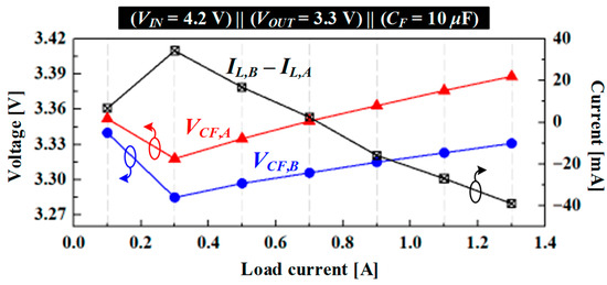
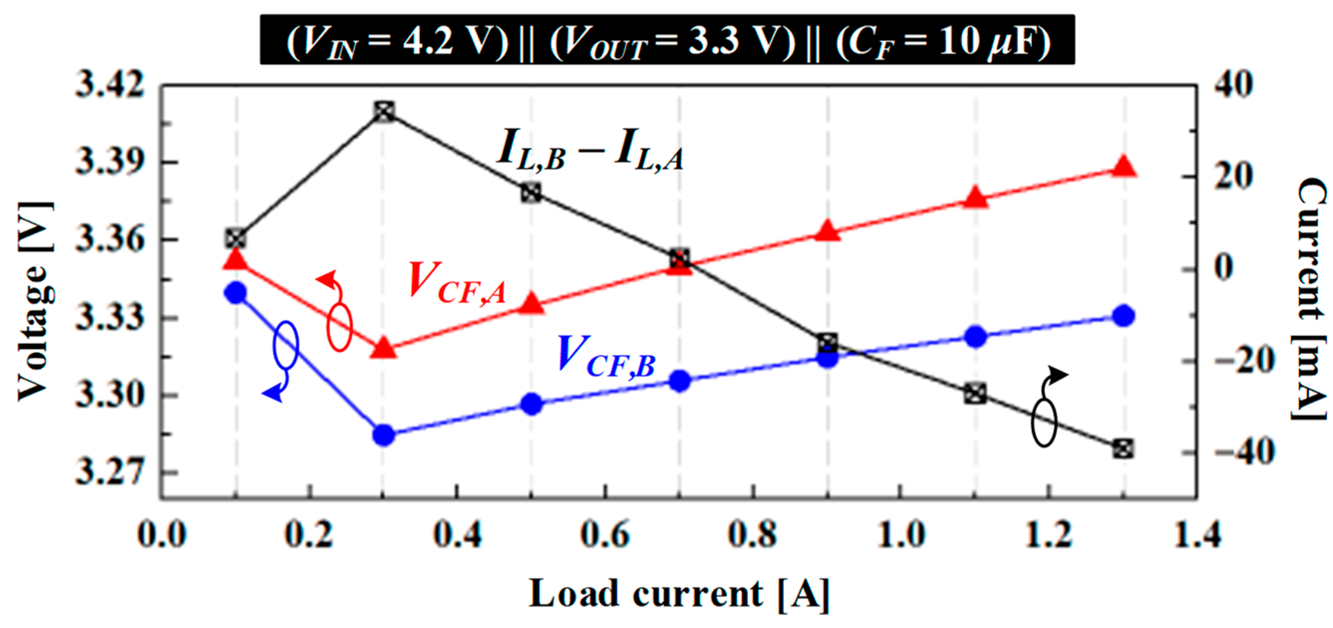
Figure 23 shows the simulation results of the inductor current mismatch caused by the voltage imbalance between the two flying capacitors. As ILOAD increases from 100 mA to 1.3 A, the maximum difference between the two average IL,A and IL,B is calculated to be 38.9 mA when the voltage mismatch reaches 57 mV.
Figure 23.
Current mismatch due to the voltage imbalance between two CFs.
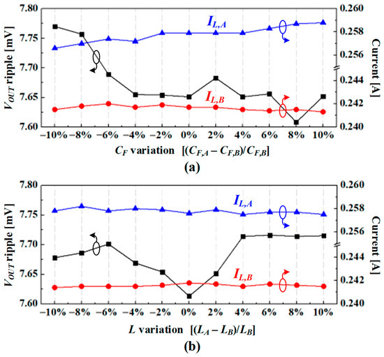
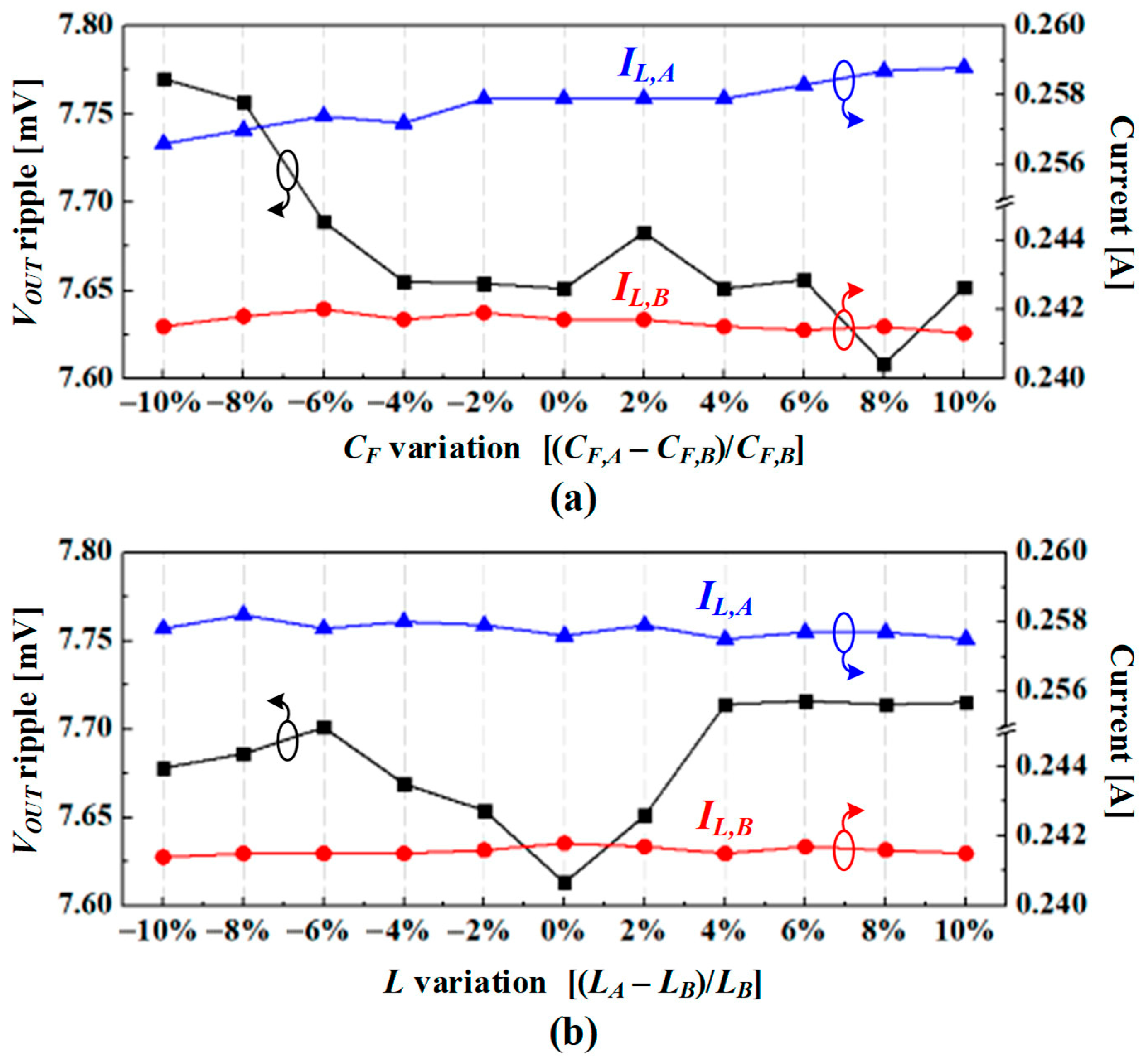
In practical implementations, the capacitor and inductance values of the two power stages may not be perfectly identical. To investigate the impact of such component mismatches, parametric simulations were performed by varying the CF and inductance values. Figure 24a,b shows the variations in the VOUT ripple and the inductor currents of each phase due to the mismatch of CF and inductance, respectively. As shown in Figure 24a, when the capacitance varies by ±10%, the VOUT ripple changes by up to 1 mV (1.53%). In the case of inductance variation, the VOUT ripple changes up to 1.03 mV (1.34%) with an inductance variation of ±10%, as shown in Figure 24b.
Figure 24.
Transient waveforms with current mismatch in (a) conventional multiphase and (b) proposed dual-phase buck–boost converters.
Future work may focus on addressing the limitations discussed above. For example, a current-balancing technique that senses the voltages of the two flying capacitors and compensates for their voltage difference could be introduced to mitigate the current imbalance which occurs in the dual-phase architecture. Such an approach could help maintain better current balance between the two phases and further improve the overall performance of the dual-phase converter.
Author Contributions
Conceptualization, S.M. and J.C.; methodology, S.M. and J.H.; validation, S.M., J.C. and G.K.; formal analysis, S.M.; investigation, G.K. and J.K.; resources, I.P.; data curation, I.P. and J.H.; writing—original draft preparation, S.M.; writing—review and editing, S.M. and I.P.; visualization, J.K.; supervision, I.P.; project administration, I.P.; funding acquisition, I.P. All authors have read and agreed to the published version of the manuscript.
Funding
This work was supported by INHA UNIVERSITY Research Grant.
Data Availability Statement
The original contributions presented in this study are included in the article. Further inquiries can be directed to the corresponding author.
Acknowledgments
The chip fabrication and EDA tool were supported by the IC Design Education Center (IDEC), Korea.
Conflicts of Interest
The authors declare no conflicts of interest.
Symbols
The following symbols are used in this manuscript:
| VIN | Input voltage |
| VOUT | Output voltage |
| IIN | Input current |
| iDLV | Output delivery current |
| iL | Inductor current |
| CF | Flying capacitor |
| ILOAD | Load current |
| iC | Capacitor current |
| TCK | Clock cycle |
| PCD | Conduction loss |
| Φ1 | Switching phase 1 |
| Φ2 | Switching phase 2 |
| Φ3 | Switching phase 3 |
| MPROP | Conversion ratio of the proposed method |
| IL | Average value of inductor current |
| IC,1 | Capacitor current during Φ1 |
| COUT | Output capacitor |
| PCD,PROP | Conduction loss of the proposed method |
| RON | On-resistance of each power switch |
| RDC | DCR of the inductor |
| fCK | Clock frequency |
| iC,1 | Capacitor current during Φ1 |
| τ | Time constant |
| iL,3 | Inductor current during Φ3 |
| iC,1,pp | Peak-to-peak of iC,1 |
| iC,1,pp,norm | Normalized capacitor current ripple |
| VERR | Error voltage |
| PSW | Switching loss |
| VCB | Voltage at the bottom node of the flying capacitor |
| VOS | Offset voltage |
| M1 | Positive-input transistor of the comparator |
| MOS | Offset injecting transistor |
| VCTRL | Control voltage of MOS |
| TSETTLE | Settling time |
| iL,rms | RMS inductor current |
| IL,A | Inductor current of 0° stage |
| IL,B | Inductor current of 180° stage |
Abbreviations
The following abbreviations are used in this manuscript:
| DPBB | Dual-phase hybrid buck-boost |
| DCR | DC resistance |
| DCM | Discontinuous conduction mode |
| ZCD | Zero-current detector |
| D | Duty cycle |
| PCE | Power conversion efficiency |
| EMI | Electromagnetic interference |
References
- Ju, Y.-M.; Shin, S.-U.; Huh, Y.; Park, S.-H.; Bang, J.-S.; Kim, K.-D.; Choi, S.-W.; Lee, J.-H.; Cho, G.-H. A hybrid inductor-based flying-capacitor-assisted step-up/-step-down dc–dc converter with 96.56% efficiency. In 2017 IEEE International Solid-State Circuits Conference (ISSCC); IEEE: New York, NY, USA, 2017; pp. 184–185. [Google Scholar]
- Ko, M.W.; Kim, K.D.; Woo, Y.J.; Shin, S.U.; Han, H.K.; Huh, Y.; Kang, G.G.; Cho, J.H.; Lim, S.J.; Park, S.H.; et al. A 97% high-efficiency 6μs fast-recovery-time buck-based step-up/down converter with embedded 1/2 and 3/2 charge-pumps for Li-ion battery management. In 2018 IEEE International Solid-State Circuits Conference-(ISSCC); IEEE: New York, NY, USA, 2018; pp. 428–429. [Google Scholar]
- Lin, Y.A.; Huang, T.P.; Ou-Yang, Y.Z.; Wu, Z.R.; Chen, K.H.; Lin, Y.H.; Lin, M.H.; Chou, H.T. A right-half-plane zero-free buck–boost dc–dc converter with 97.46% high efficiency and low output voltage ripple. In 2019 Symposium on VLSI Circuits; IEEE: New York, NY, USA, 2019; pp. C174–C175. [Google Scholar]
- Jeon, J.; Maeng, J.; Park, I.; Kim, H.; Kim, C. A hybrid dc–dc converter capable of supplying heavy load in step-up and step-down mode. In 2021 IEEE International Symposium on Circuits and Systems (ISCAS); IEEE: New York, NY, USA, 2021; pp. 1–5. [Google Scholar]
- Shin, S.; Hong, S.; Lee, H.; Cho, G. High-efficiency hybrid dual-path step-up dc–dc converter with continuous output-current delivery for low output voltage ripple. IEEE Trans. Power Electron. 2020, 35, 6025–6038. [Google Scholar] [CrossRef] [Scilit]
- Huh, Y.; Hong, S.; Cho, G. A hybrid structure dual-path step-down converter with 96.2% peak efficiency using 250-mΩ large-DCR inductor. IEEE J. Solid-State Circuits 2019, 54, 959–967. [Google Scholar] [CrossRef] [Scilit]
- Shin, H.; Jang, D.; Kang, G.G.; Kim, J.; Kim, C.; Ha, S.; Je, M. A 96.6%-efficiency continuous-input-current hybrid dual-path buck–boost converter with single-mode operation and non-stopping output current delivery. In 2021 Symposium on VLSI Circuits; IEEE: New York, NY, USA, 2021; pp. 1–2. [Google Scholar]
- Huang, M.; Lu, Y.; Hu, T.; Martins, R.P. A hybrid boost converter with cross-connected flying capacitors. IEEE J. Solid-State Circuits 2021, 56, 2102–2112. [Google Scholar] [CrossRef] [Scilit]
- Park, I.; Maeng, J.; Jeon, J.; Kim, H.; Kim, C. A four-phase hybrid step-up/down converter with RMS inductor current reduction and delay-based zero-current detection. IEEE Trans. Power Electron. 2022, 37, 3708–3712. [Google Scholar] [CrossRef] [Scilit]
- Wang, Y.O.G.; Zhang, J.; Guan, Y.; Xu, D.G. Analysis and design of a two-phase series capacitor dual-path hybrid dc–dc converter. IEEE Trans. Power Electron. 2022, 37, 9492–9502. [Google Scholar] [CrossRef] [Scilit]
- Chen, C.; Liu, J.; Lee, H. A 2-MHz 9–45-V input high-efficiency three-switch ZVS step-up/down hybrid converter. IEEE J. Solid-State Circuits 2021, 56, 855–865. [Google Scholar] [CrossRef] [Scilit]
- Tang, N.; Hong, W.; Nguyen, B.; Zhou, Z.; Kim, J.-H.; Heo, D. Fully integrated switched-inductor-capacitor voltage regulator with 0.82-A/mm2 peak current density and 78% peak power efficiency. IEEE J. Solid-State Circuits 2021, 56, 1805–1815. [Google Scholar] [CrossRef] [Scilit]
- Baek, J.; Nomiyama, T.; Park, S.; Jung, Y.-H.; Kim, D.; Han, J.; Bang, J.-S.; Lee, Y.; Kim, I.-H.; Paek, J.-S.; et al. A voltage-tolerant three-level buck–boost dc–dc converter with continuous transfer current and flying capacitor soft charger achieving 96.8% power efficiency and 0.87μs/V DVS rate. In 2020 IEEE International Solid-State Circuits Conference-(ISSCC); IEEE: New York, NY, USA, 2020; pp. 202–203. [Google Scholar]
- Hardy, C.; Ramadass, Y.; Scoones, K.; Le, H. A flying-inductor hybrid dc–dc converter for 1-cell and 2-cell smart-cable battery chargers. IEEE J. Solid-State Circuits 2019, 54, 3292–3305. [Google Scholar] [CrossRef] [Scilit]
- Stala, R.; Waradzyn, Z.; Folmer, S. Input current ripple reduction in a step-up dc–dc switched-capacitor switched-inductor converter. IEEE Access 2022, 10, 19890–19904. [Google Scholar] [CrossRef] [Scilit]
- Cho, Y.; Lee, K.C. Noninverting buck–boost dc–dc converter using a duobinary-encoded single-bit delta-sigma modulator. IEEE Trans. Power Electron. 2020, 35, 484–495. [Google Scholar] [CrossRef]
- Tang, J.; Guo, T.; Kim, J.S.; Roh, J. A current-mode four-phase synchronous buck converter with dynamic dead-time control. IEEE Access 2021, 9, 81078–81088. [Google Scholar] [CrossRef] [Scilit]
- Huang, Y.; Kuo, T.; Huang, S.; Fang, K. A four-phase buck converter with capacitor-current-sensor calibration for load-transient-response optimization that reduces undershoot/overshoot and shortens settling time to near their theoretical limits. IEEE J. Solid-State Circuits 2018, 53, 552–568. [Google Scholar] [CrossRef] [Scilit]
- Luo, Z.; Zeng, L.; Lau, B.; Lian, Y.; Heng, C.-H. A sub-10 mV power converter with fully integrated self-start, MPPT, and ZCS control for thermoelectric energy harvesting. IEEE Trans. Circuits Syst. I Reg. Papers 2018, 65, 1744–1757. [Google Scholar] [CrossRef] [Scilit]
- Shang, Z.; Zhao, Y.; Gou, W.; Geng, L.; Lian, Y. 83.9% efficiency 100-mV self-startup boost converter for thermoelectric energy harvester in IoT applications. IEEE Trans. Circuits Syst. II Exp. Briefs 2020, 67, 1654–1658. [Google Scholar] [CrossRef] [Scilit]
- Shrivastava, A.; Roberts, N.E.; Khan, O.U.; Wentzloff, D.D.; Calhoun, B.H. A 10 mV-input boost converter with inductor peak current control and zero detection for thermoelectric and solar energy harvesting with 220 mV cold-start and −14.5 dBm, 915 MHz RF kick-start. IEEE J. Solid-State Circuits 2015, 50, 1820–1832. [Google Scholar] [CrossRef] [Scilit]
- Mu, J.; Liu, L. A 12 mV input, 90.8% peak efficiency CRM boost converter with a sub-threshold startup voltage for TEG energy harvesting. IEEE Trans. Circuits Syst. I Reg. Papers 2018, 65, 2631–2640. [Google Scholar] [CrossRef] [Scilit]
- Radin, R.L.; Sawan, M.; Schneider, M.C. An accurate zero-current-switching circuit for ultra-low-voltage boost converters. IEEE Trans. Circuits Systs. II Exp. Briefs 2021, 68, 1773–1777. [Google Scholar] [CrossRef] [Scilit]
- Katic, J.; Rodriguez, S.; Rusu, A. A dual-output thermoelectric energy harvesting interface with 86.6% peak efficiency at 30 μW and total control power of 160 nW. IEEE J. Solid-State Circuits 2016, 51, 1928–1937. [Google Scholar] [CrossRef] [Scilit]
- Lim, B.-M.; Seo, J.-I.; Lee, S.-G. A colpitts oscillator-based self-starting boost converter for thermoelectric energy harvesting with 40-mV startup voltage and 75% maximum efficiency. IEEE J. Solid-State Circuits 2018, 53, 3293–3302. [Google Scholar] [CrossRef] [Scilit]
- Alhawari, M.; Mohammad, B.; Saleh, H.; Ismail, M. An efficient zero current switching control for L-based dc–dc converters in TEG applications. IEEE Trans. Circuits Syst. II Exp. Briefs 2017, 64, 294–298. [Google Scholar] [CrossRef] [Scilit]
- Su, F.; Ki, W.-H.; Tsui, C.-Y. Ultra fast fixed-frequency hysteretic buck converter with maximum charging current control and adaptive delay compensation for DVS applications. IEEE J. Solid-State Circuits 2008, 43, 815–822. [Google Scholar] [CrossRef]
- Park, I.; Maeng, J.; Shim, M.; Jeong, J.; Kim, C. A high-voltage dual-input buck converter achieving 52.9% maximum end-to-end efficiency for triboelectric energy-harvesting applications. IEEE J. Solid-State Circuits 2020, 55, 1324–1336. [Google Scholar] [CrossRef] [Scilit]
- Cho, D.; Cho, H.; Oh, S.; Jung, Y.; Ha, S.; Kim, C.; Je, M. A High-Efficiency Single-Mode Dual-Path Buck-Boost Converter with Reduced Inductor Current. IEEE J. Solid-State Circuits 2023, 58, 720–731. [Google Scholar] [CrossRef] [Scilit]
- Mishra, A.; Zhu, W.; Wicht, B.; Smedt, V.D. An All-1.8-V-Switch Hybrid Buck–Boost Converter for Li-Battery-Operated PMICs Achieving 95.63% Peak Efficiency Using a 288-m DCR Inductor. IEEE Trans. Power Electron. 2023, 38, 3444–3454. [Google Scholar] [CrossRef] [Scilit]
- Kim, D.-H.; Kim, H.-S. A Power-Efficient Single-Mode Buck-Boost DC–DC Converter With Bilaterally Symmetrical Hybrid Topology. IEEE J. Solid-State Circuits 2024, 59, 4137–4149. [Google Scholar] [CrossRef] [Scilit]
- Sun, M.; Yang, Z.; Joshi, K.; Mandal, D.; Adell, P.; Bakkaloglu, B. A 6 A, 93% efficiency, 4-phase digitally synchronized hysteretic buck converter with ±1.5% frequency and ±3.6% current-sharing error. IEEE J. Solid-State Circuits 2017, 52, 3081–3094. [Google Scholar] [CrossRef]
- Cho, D.; Cho, H.; Oh, S.; Jung, Y.; Ha, S.; Kim, C.; Je, M. A single-mode dual-path buck-boost converter with reduced inductor current across all duty cases achieving 95.58% efficiency at 1A in boost operation. In 2022 IEEE Custom Integrated Circuits Conference (CICC); IEEE: New York, NY, USA, 2022; pp. 1–2. [Google Scholar]

Disclaimer/Publisher’s Note: The statements, opinions and data contained in all publications are solely those of the individual author(s) and contributor(s) and not of MDPI and/or the editor(s). MDPI and/or the editor(s) disclaim responsibility for any injury to people or property resulting from any ideas, methods, instructions or products referred to in the content. |
© 2026 by the authors. Licensee MDPI, Basel, Switzerland. This article is an open access article distributed under the terms and conditions of the Creative Commons Attribution (CC BY) license.