


Abstract
A new architecture of FPGA-based Moore finite state machine (FSM) is proposed, as well as the corresponding method of synthesis. The proposed architecture of FSM circuit includes two cores of partial Boolean functions. The first core is based on functional decomposition, the second core is based on structural decomposition. Under certain conditions, the proposed method improves both spatial and temporal characteristics of FSM circuits. The FSM states have two codes. The first of them is a maximum binary code (MBC) having minimum possible number of bits. The second code is a partial state code representing a state as the element of some class of compatibility. The method can be applied if Moore FSM circuits are implemented using look-up table (LUT) elements of field-programmable gate arrays. To improve characteristics of resulting FSM circuits, the classes of pseudoequivalent states are used. This allows diminishing the numbers of literals in sum-of-products representing partial input memory functions. The first core is multi-level. For the second core, all partial functions are generated by single-LUT circuits. These cores form the first level of FSM circuit. The LUTs of the second level generate bits of MBCs. These codes are used by the third circuit level for generating both FSM outputs and partial state codes. An example of synthesis is shown. The experiments are conducted using a known library of benchmark Moore FSMs. The experiments show that the proposed approach can be used for complex FSMs where the total number of FSM inputs and state variables is at least twice the number of inputs of the base LUT. The results of experiments show that the proposed method allows improving both the spatial and temporal characteristics for complex FSMs compared with their counterparts based on other known design methods.
1. Introduction
It is known that the majority of modern digital systems includes a lot of various sequential blocks [1,2]. These sequential blocks can be used as (1) control units of computers [3,4,5,6,7]; (2) controllers of various protocols used in embedded systems [8]; (3) blocks of hyper-tangent and exponential functions [9]; (4) different blocks for integral stochastic computing [10]; (5) activation functions of deep neural networks [11,12]; (6) different stages of cascaded digital processing systems [13,14]. A lot of other examples could be added [15,16,17,18,19,20,21,22,23]. This wide range of applications explains continuous interest in optimizing characteristics of sequential blocks. This requires working out new design methods of these blocks. Very often, the sequential blocks are represented using the model of Moore finite state machine (FSM) [24,25]. This paper is devoted to optimizing spatial characteristics of Moore FSMs implemented with field-programmable gate arrays (FPGAs) [26,27,28].
Various FPGA chips are applied for implementing the digital systems [29,30]. Due to this, we choose these chips as a base for implementing circuits of Moore FSMs. Leading experts are sure that FPGAs will be used for at least three next decades [31]. In this article, we discuss a case when logic circuits of Moore FSMs are implemented with look-up table (LUT) elements, programmable flip-flops, dedicated multiplexers, programmable interconnections, and a synchronization tree.
A LUT is a single-output logic block having inputs [26,28]. If some Boolean function depends on up to arguments, then it could be generated by a single LUT [32,33]. But the number of LUT inputs is very small: it does not exceed six [26,28,30]. Very often, this peculiarity is the cause of using the methods of functional decomposition (FD). These methods turn systems of Boolean functions (SBFs) representing logic circuits of Moore FSMs [33,34] into compositions of partial functions. This approach produces rather Moore FSM circuits having a lot of logic levels and a very complicating system of interconnections [35].
To improve the main characteristics of LUT-based FSM circuits, it is necessary to reduce the numbers of LUTs used and simplify the system of interconnections. The problem of reducing the values of LUT counts is known as a problem of improving the spatial characteristics [36,37]. As a rule, optimizing the values of LUT counts reduces the chip area occupied by an FSM circuit. In turn, it reduces the value of power consumption [38]. It is very important to improve the spatial characteristics in such a way that this does not deteriorate tremendously the temporal characteristics of resulting circuits. In this article, we propose a method which allows optimizing spatial characteristics without increasing either the cycle time or the power consumption of produced Moore FSM circuit.
The spatial characteristics of a LUT-based FSM circuit is determined mostly by the value of LUT count and the system of inter-LUT interconnections. The best way for reducing the area required by a circuit is the reducing the value of LUT count for a given circuit. But optimizing the system of interconnections is very important, too. Two factors determine this importance. The first factor: in modern chips, interconnection delay dominates logic delay [32,39]. The second factor: around 70% of power is consumed by the system of interconnections [40]. So, the optimization of the interconnect system is necessary to diminish the power consumption and increase the value of maximum operating frequency of a particular FSM circuit [2].
Results of research [29] prove that value SL = 6 allows obtaining the optimal trade-off for such characteristics of LUTs as the occupied chip area, performance, and consumed energy. Therefore, we cannot expect the growth for the number of LUT inputs. But the complexity of FPGA-based projects is constantly growing [19,41]. So, it is necessary to develop efficient methods of technology mapping for improving the basic characteristics of LUT-based circuits.
In this paper, we propose a novel design method whose purpose is improving the spatial characteristics of LUT-based Moore FSMs. The method uses some specifics of the model of Moore FSM discussed further. The main idea of the proposed method is reduced to adding an SD-based core of partial Boolean functions (PBFs) to FD-based Moore FSM architecture. The proposed method leads to double-core FSM architectures whose circuits have less values of LUT counts than their single-core FD-based counterparts.
The paper includes five more sections. They contain the following information. Section 2 includes basic information about the FSM model used and logic elements. Section 3 discusses the state of the art in the LUT-based design of sequential devices. Section 4 represents the essence of the proposed method. Section 5 includes a synthesis example. Section 6 is devoted to analysis of results of conducted experiments. A brief conclusion sums up the results obtained in the paper.
2. Background Information
As a rule, modern FPGAs include different configurable logic blocks (CLBs) and a matrix of programmable interconnections [26,27,28]. Our current paper is devoted to the case when CLBs include LUTs, dedicated multiplexers and programmable flip-flops. Inside each CLB, the LUT output and a flip-flop input are directly connected (without using programmable multiplexers). The flip-flops can be used as a state memory of sequential blocks [24].
The main specific of LUT is a very limited number of inputs, . In modern FPGAs, the value of does not exceed six [28,42]. This leads to the necessity of functional decomposition of Boolean functions depending on at least 1+ arguments [33]. As a rule, the FD-based FSM circuits are multi-level. Moreover, they posses the irregular systems of interconnections. As it is mentioned in [2], the functional decomposition leads to FSM circuits with “spaghetti-type” interconnections.
A Moore FSM is defined as a six-component vector [24], where is a finite set of states, is a finite set of inputs, is a finite set of outputs, is a transition function, is an output function, and is an initial state. A Moore FSM can be represented using various approaches. In this paper, we use state transition graphs (STGs) and state transition tables (STTs) of Moore FSMs [1,24].
An STG has M nodes. Each node corresponds to a single state . Near each node, the collections of outputs are written where . The interstate transitions are represented by arcs directed from current states into states of transitions. If an FSM has H transitions, then its STG has H arcs. Above the arc, the input signal is written. This signal determines the transition from a current state into the next state. The signal is a conjunction of inputs (or their compliments) determining a particular transition.
An STT can be viewed as a tabular representation of a corresponding STG. Each line of STT corresponds to a unique arc of STG. The STT has the columns [24]: (the current state), (the state of transition), , h. The collection of outputs generated in the state is shown in the column . This allows to implement the output function of Moore FSMs where outputs do not depend on FSM inputs. There is the transparent connection between these two forms of FSM representation.
Three operations should be executed to construct SBFs representing a Moore FSM circuit [24]. First of all, it is necessary to execute a state assignment [43,44,45]. During this step, each state is represented by a binary code . In the case of maximum binary state assignment, this code consists of R bits (state variables). The minimum possible number of state code bits, R, is determined as
Let us point out that maximum binary codes (MBCs) are used, for example, in well-known academic systems SIS [46] and ABC [47] of Berkeley, as well as in industrial CAD tools Vivado [48] and Quartus [49].
The second step is a constructing the sets of state variables and input memory functions (IMFs) . The IMFs are used for generating the code of the state of transition; they allow to implement the transition function of Moore FSM. The third step is reduced to transformation of initial STT into a direct structure table (DST). Compared to STT, an equivalent DST has three additional columns: , , . The column includes IMFs corresponding to state variables in a code written in the line of DST.
State codes should be unchangeable during a cycle of operation. To provide this property, a special register (RG) is used. This block includes R flip-flops. Its operation is controlled by inputs of synchronization (Clock) and reset (Start). As a rule, D flip-flops are used in LUT-based FSMs [43]. Input memory functions can change the RG content (of course, the content may stay the same if the relation takes place for a given transition).
A direct structure table is a base for creating two systems of functions. These systems are the following:
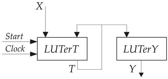
The SBFs (2) and (3) are the base for designing a logic circuit of Moore FSM (Figure 1) [50]. In the paper, we use the symbol to show that a particular block’s circuit includes only LUT-based CLBs. If some block generates IMFs, then outputs of corresponding flip-flops are treated as registered outputs of this block.
Figure 1.
Structural diagram of LUT-based Moore FSM .
In Moore finite state machine , the block generates IMFs represented by (2), the block generates outputs represented by SBF (3). If a function is generated by some LUT, then the corresponding flip-flop’s output is used to enter other CLBs of an FSM circuit. The flip-flops represent the block RG which is hidden inside the block . Because of it, the pulses Start and Clock enter the . Obviously, the state register RG is hidden. Due to this, the RG is not shown as a separate block of FSM .
As shown in [51], using two specifics leads to optimizing the spatial characteristics of Moore FSM circuits. The first specific is an existence of classes of pseudoequivalent states (PES). The second specific is a dependence of FSM outputs only on state variables . Using the first specific, it is possible to minimize the number of arguments in sum-of-products (SOP) of functions included into SBF (2). Using the second specific allows reducing the number of arguments in SOPs of functions . We propose to use these specifics in LUT-based design. This may result in reducing the numbers of LUTs and their levels in circuits of blocks (using the first specific) and (using the second specific). We discuss these issues in the following sections.
3. State of the Art
The process of technology mapping has been always associated with solution of some optimization problems [43]. As a rule, three classical optimization problems arise in the process of designing FPGA-based FSMs [2]. These problems are: (1) the improving the spatial characteristics, (2) the increase in performance, and (3) the reduction in power consumption. The current paper is aimed at the improving the spatial characteristics. In LUT-based circuits, the spatial characteristics are mostly determined by the numbers of LUT (LUT count) used and inter-CLB interconnections [2].
Of course, some other problems are connected with designing FSM circuits. For example, the testability of FPGA-based circuit should be improved [52,53,54,55]. Also, the circuits should require defense against various malicious attacks [56,57]. In many practical cases, it is necessary to increase the reliability of FSM circuits [58]. To provide the required qualities for an FSM circuit, some additional internal chip resources must be used [58]. This additional blocks consume LUTs, interconnections, and power. We do not discuss these problems because each of them requires a separate paper devoted exclusively to a particular problem.
Let us denote as the number of literals [1] in SOP of a function . As shown in [2], the number of logic levels in the resulting circuit implementing the function depends significantly on the condition
The violation of Condition (4) leads to producing multi-level FSM circuits. In this case, the problem of hardware reduction arises. For multi-level circuits, it is quite possible that the same inputs and state variables appear on more than a single logic level. It leads to circuits with the spaghetti-type interconnections. The results of experiments conducted by the authors of [59] proved that the regularization of interconnections leads to decreasing the power consumption compared with equivalent circuits having irregular interconnections.
To improve the spatial characteristics LUT-based FSM circuits, three main approaches can be used:
- 1.
- 2.
- The optimal encoding of internal FSM states [1,2,62];
- 3.
- The transformation of FSM circuit (the structural decomposition) [2,59,63,64].
The essence of FD is the following. If Condition (4) is violated, then a function is broken down into smaller and smaller components. These components are partial Boolean functions (PBFs). This process is terminated when any PBF depends on no more than arguments. The FD-based solutions are used very often in the process of FPGA-based technology mapping [61,65].
Using the methods of FD leads to appearing partial Boolean functions. These partial functions are much simpler than the initial functions included in Systems (2) and (3). If Condition (4) takes place, then there are only LUTs in the logic circuit of Moore FSM . Otherwise, the circuit includes elements. The program tools for executing FD are integral parts of both academic [46,47] and industrial [66,67,68] CAD systems.
It is known that for the same FSM, different outcomes of state assignment result in the FSM circuit with different amount of hardware [69]. The optimal state assignment is a process allowing maximum possible minimization of SBFs (2) and (3). This task could be solved using, for example, the algorithm JEDI [46]. We think that JEDI is a part of the system ABC developed by Berkely [47].
Let us point out that each literal of SOP corresponds to a wire in the FSM circuit. So, to reduce the number of interconnections, it is necessary to reduce the numbers of literals in functions . Therefore, the optimal state assignment must be performed regardless of holding Condition (4).
Various state assignment strategies can be found in modern industrial CAD tools. For example, the design tool Vivado [48,67] of AMD Xilinx uses: the automatic state assignment; One-hot (R = M); compact; Gray codes; Johnson codes; speed encoding; sequential encoding.
In the case of Moore FSM, the area reduction can be achieved via taking into account the existence of pseudoequivalent states [50]. The states are pseudoequivalent if () = (). Using this definition, it is possible to find a partition of the set A by classes of PES. If , then the optimal state assignment is reduced to finding state codes such that each class is represented by a minimum possible number of generalized intervals of R-dimensional Boolean space [50]. Such state assignment can be executed using, for example, the methods in [70].
The main idea of SD-based methods [50] is reduced to elimination of a direct dependency of functions on inputs To eliminate direct dependence, a set of some additional functions is constructed. These functions are divided by systems. Each system of new functions determines a separate block with its unique sets of input and output variables. The classical SD methods use additional variables instead of FSM inputs and maximum binary codes instead of FSM outputs [24]. These methods are thoroughly discussed, for example, in [2].
As shown in [2], the structural decomposition leads to reduced number of literals in SOPs of functions as compared to Functions (2) and (3). In turn, this leads to reducing the values of LUT counts in circuits of FSMs as compared to their counterparts based on functional decomposition.
Let the transitions from the state depend on FSM inputs. Let for some Moore FSM Condition (4) be violated, whereas the following condition holds:
In this case, reducing hardware in LUT-based Moore FSMs is possible due to using the method of twofold state assignment [50].
The term “twofold state assignment” means that each state has two codes: the maximum binary code and a partial state code . To create partial state codes, the additional variables are used. This method can be applied if for each state the following condition takes place:
Let us explain this approach. The method is based on finding a partition of the set A by classes of compatible states. A class includes states. Each state is encoded by two codes (MBC and ). The code requires state variables, where
To create partial codes of states , the variables are used.
The variables are combined into a single set having elements:
The elements create extended state codes (ESC) .
Each class corresponds to some block . This block generates the following partial functions:
In (9), the symbol stands for a set of IMFs generating during the transitions from the states , the symbol stands for a set of FSM inputs causing transitions from the states . These K blocks create the first level of FSM circuit.
A block (the functional assembler) generates the final values of IMFs:
This block creates the second logic level.
The third logic level includes two blocks, and . The block generates functions from SBF (3). The block generates the extended state codes. Due to this, the block implements SBF:
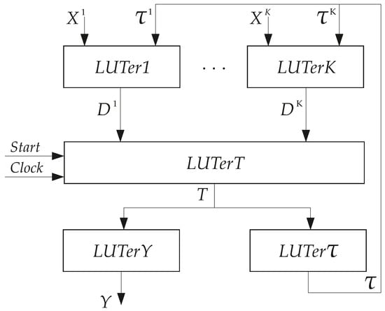
The architecture of Moore FSM is shown in Figure 2.
Figure 2.
Structural diagram of LUT-based Moore FSM .
The block includes R primary–secondary flip-flops combined into state register. The register is hidden inside CLBs of . Pulses Start and Clock control the operation of RG.
The states of each class are compatible. This means [50] that the states satisfy the condition
The symbol in (12) stands for the number of elements in the set .
As shown in [2], this approach improves spatial characteristics of LUT-based FSM circuits compared with the characteristics of FD-based equivalents. But the model cannot be applied if the following condition takes place for at least a single state :
Obviously, if (13) holds, then it is impossible to place such a state into any class . In this case, the model should be used. This means that methods of FD should be applied to implement the logic circuit of this particular Moore FSM.
In the current paper, we propose a design method which allows using twofold state assignment only for some part of FSM circuit. In this case, the FSM architecture includes two cores of PBFs. One core is based of FD. Another core is based on twofold state assignment.
4. Background of Proposed Method
Let some Moore FSM S be represented by its STG. Let us encode FSM states by MBCs having minimum number of bits determined as (1). Let us construct the DST of Moore FSM S. Now, we know the numbers of FSM states, inputs, and code bits, R. Knowing this, we can divide the set of states A by two disjoint sets, and ( ). For the states , Condition (13) holds. Obviously, for the states , Condition (13) is violated. The set determines a set including FSM inputs which cause transitions from states . There are elements in the set . The set determines a set including FSM inputs which cause transitions from states . The set contains states.
Let us encode states by partial codes having variables, where
To create these codes, we use variables from a set . Using DST, we can find the set of partial input memory functions . This set includes IMFs generating during transitions from states . Using the part of DST with current states , the following SBF can be created:
Next, we propose to apply the procedure of twofold state assignment for the states . Let us find the partition of the set by K classes of compatible states. This can be achieved using the greedy algorithm discussed in [50]. The states are encoded by partial codes using elements of the set .
After executing the partial state assignment, we create the DST for states . This allows finding SBFs (9). The final values of input memory functions could be generated using the following SBF:
Finally, we should find an SBF representing dependences of variables and on the state variables . The SBF (11) gives this dependence for variables . The second dependence is represented as
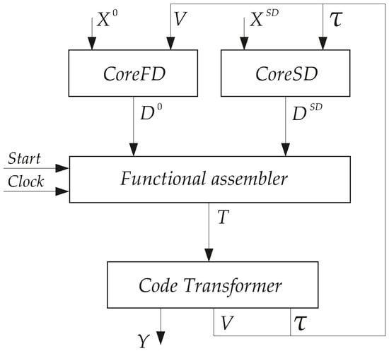
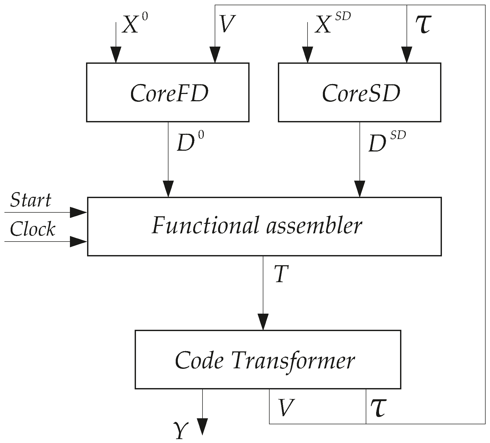
Systems (9), (11), (15)–(17) determine an architecture of Moore FSM with two cores of partial Boolean functions. The generalized architecture of FSM is shown in Figure 3.
Figure 3.
Generalized architecture of FSM .
The generalized architecture (Figure 3) consists of three levels of logic blocks. The first level includes two cores of PBFs. The includes LUTs generating functions from SBF (15). This core’s circuit is multi-level. The implementation of the LUT-based circuit of the is connected with applications of various methods of FD [61]. This core is responsible for reducing the value of maximum operating frequency of resulting FSM circuit.
The includes LUTs generating functions from SBF (9). The core’s circuit is single-level. The implementation of corresponding LUT-based circuit is straightforward.
The second logic level is a functional assembler. The final values of IMFs (16) are generated by LUTs of this block. The function is represented by partial functions. It is possible that the block includes only a single level of LUTs. This is possible if the following condition takes place for all input memory functions:
If (18) is violated, then this circuit includes at least two levels of LUTs. The block includes a distributed register RG controlled by signals Start and Clock.
The code transformer represents the third logic level of FSM . Its LUTs generate partial state Variables (11) and (17) together with FSM outputs (3). This block is single-level if the following condition holds:
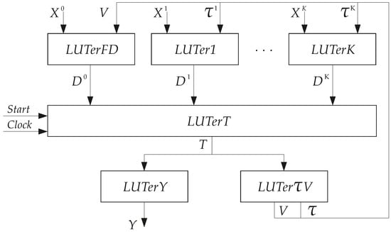
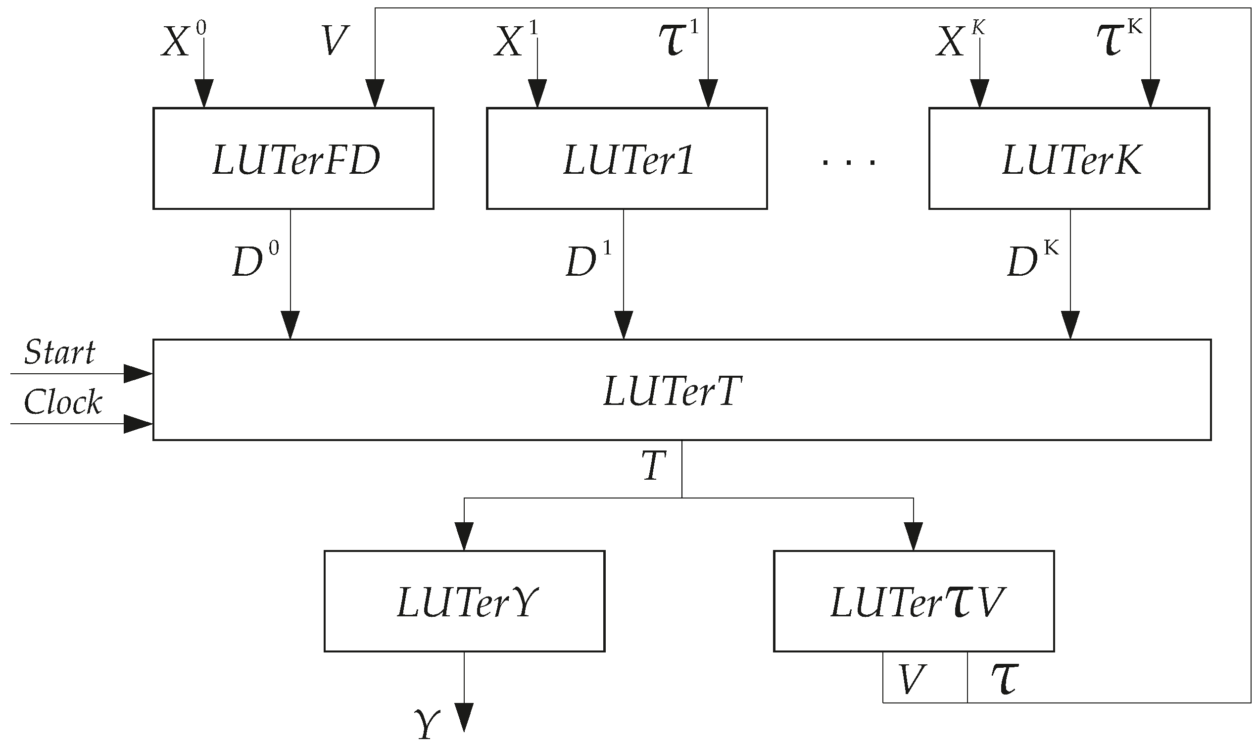
Each block (Figure 3) is represented by some blocks of LUTs. The resulting architecture of FSM is shown in Figure 4.
Figure 4.
LUT-based architecture of Moore FSM .
There is a transparent connection between architectures shown in Figure 3 and Figure 4. The block is represented by the block (Figure 4). The block CoreSD is represented by K blocks . The functional assembler is represented by the block Finally, two blocks of LUTs represent the code transformer (Figure 3). The block generates FSM outputs. The block generates variables used for creating partial state codes.
In this paper, we propose a synthesis method for Moore FSM . We assume that an FSM is represented by either STT or STG. In the latter case, the initial STG should be transformed into the equivalent STT. There are the following steps in the proposed synthesis method:
- 1.
- Dividing the set of states by sets and .
- 2.
- Encoding of states by partial state codes .
- 3.
- Splitting the set by K classes of compatible states.
- 4.
- Encoding of states by partial state codes .
- 5.
- Encoding of states in the way minimizing SBF (3).
- 6.
- Deriving Functions (15) from the table of block .
- 7.
- Deriving Functions (9) from tables of blocks .
- 8.
- Deriving Functions (16) from the table of functional assembler.
- 9.
- Deriving Functions (17) from the table of block .
- 10.
- Executing the technology mapping for resulting Moore FSM circuit.
5. Example of Synthesis
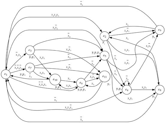
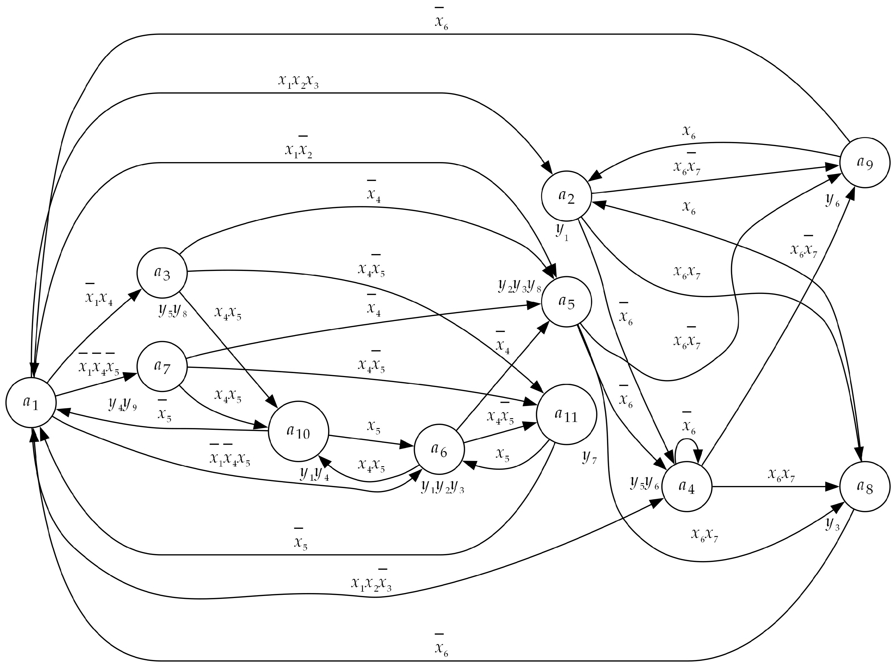
In this section, the procedure for synthesizing a Moore FSM circuit according to the proposed method is illustrated. The implementation assumes LUT elements with five inputs. As a demonstration example, we consider the FSM , which is described by the state transition table (STT) presented in Table 1 and by the corresponding state transition graph (STG) shown in Figure 5.
Table 1.
State transition table of Moore FSM S1.
Figure 5.
State transition graph representing the Moore FSM S1.
As follows from Table 1, Moore FSM S1 is characterized by the following sets: , , and . This gives the following: M = 11, L = 7, and N = 9. Table 1 consists of H = 32 rows corresponding to interstate transitions. Using Condition (1) gives R = 4. This determines the sets of state variables and IMFs . Using Table 1 and the value of , we can divide set A by two disjoint sets.
Step 1. The set exists if an STT includes states satisfying (6). In our example, Condition (6) is transformed into the following: The analysis of Table 1 allows finding the values of parameters for states Only state satisfies Condition (6). This gives the following sets: , and .
Step 2. The outcome of Step 1 shows that Using (14) gives the number of partial state variables In turn, this determines the set . Let the partial code be assigned for the state .
Step 3. To determine the partition , the greedy algorithm described in [50] is applied. This procedure iteratively constructs each class by attempting to incorporate the largest possible number of states. The main condition for including a state into a particular class is the following: the including should minimally increase the number of elements in the set .
As follows from [50], the pseudoequivalent states determine the classes of a partition of the set of states. The same inputs cause the same transitions from all states Due to this, in the case of Moore FSMs, all pseudoequivalent states are automatically placed into the same class (if it is possible, of course).
In the discussed example, there are the following classes of PES: , , , and . So, there is I = 5. Using greedy algorithm [50] gives the following partition of the set : with K = 2. This partition includes the classes and . Analysis of these classes shows that the first class includes PES from , the second class includes PES from .
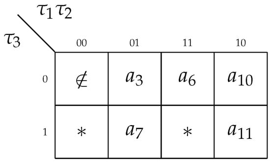
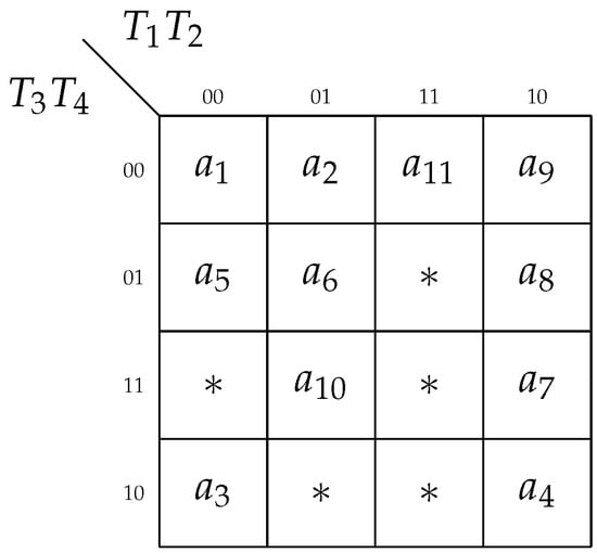
Step 4. In the discussed case, there is . Using (7) gives the numbers of bits in partial state codes: These values determine the sets , and . The variables from the set create partial state codes , where The variables from the set create partial state codes for states
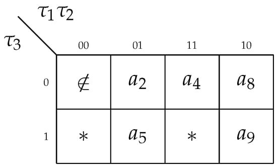
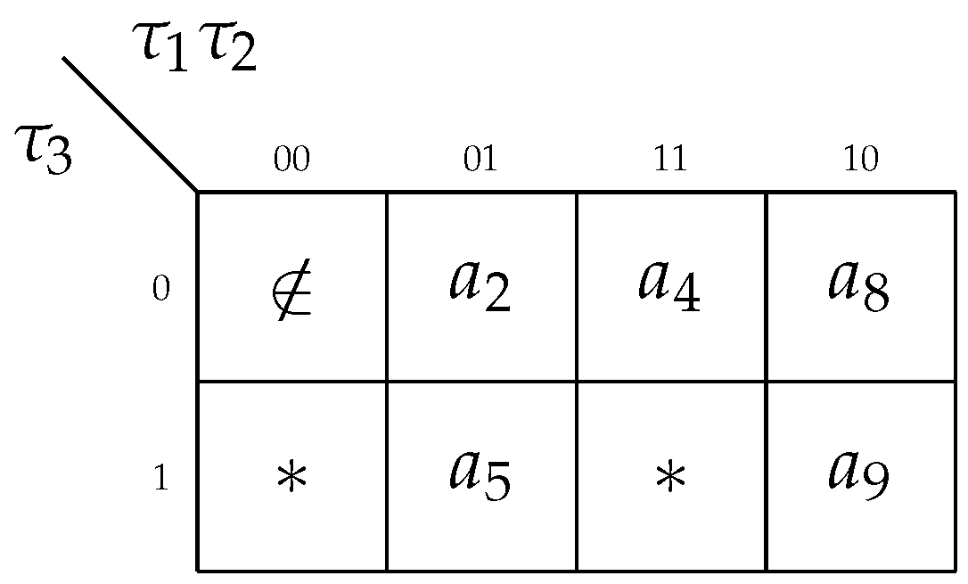
To eliminate some state variables from SOPs of Functions (9), we propose to place codes , where and , into the same generalized interval of -dimensional Boolean space. This can be achieved using, for example, the approach discussed in [70]. Using this approach, we can create the partial state codes shown in Karnaugh maps (Figure 6 and Figure 7). In these maps, the symbol «∉» shows that code 000 encodes the relation . So, code 000 represents all states which do not belong to the particular class of compatible states.
Figure 6.
Partial state codes for .
Figure 7.
Partial state codes for .
As follows from Figure 6 and Figure 7, each class of PES is represented by a single generalized interval. For example, the states are represented by the interval *1* (the symbol «*» means that the corresponding state variable is “don’t care”).
Step 5. To reduce the size of the SOP expressions of SBF (3), each FSM state should be encoded so that it can be covered by the smallest possible number of generalized intervals in the R-dimensional Boolean space [50]. This can be achieved using, for example, the method from [70]. One of the outcomes of such encoding is shown in Figure 8.
Figure 8.
Outcome of state assignment for Moore FSM S1.
Using Table 1, we can find the dependence between states and FSM outputs. For example, the output is generated in the states from the set . So, the output is represented as . The symbols stand for the conjunction of state variables corresponding to codes . As follows from Figure 8, the corresponding codes belong to interval 01**. So, the formula for should include only literals and : . Acting in the same way, we can create the following SBF:
Analysis of SBF (20) shows that its SOPs include 23 literals. Each literal corresponds to a single wire connecting a LUT input with a source of a particular state variable. Clearly, the fewer literals there are, the fewer interconnects the FSM circuit includes. The fewer interconnects, the less power is consumed and the less chip area is occupied by FSM circuit [40].
In the worst case, the SBF (3) includes literals. In the discussed case, there is RN = 36. So, the proposed style of state encoding allows eliminating 13 literals (36% of literals).
System (20) represents the circuit of . Having maximum binary and partial state codes, we can create tables for all other blocks of LUT-based circuit of Moore FSM S1.
Step 6. Table of has the following columns: (the current state belonging to the set ), , (state of transition), , , , h. Because System (3) is already obtained, there is no information about FSM outputs in the first column of this table.
In the discussed case, the table is constructed using information from Rows 1–6 of STT (Table 1). The block is represented by Table 2.
Table 2.
Table of .
Of course, partial IMFs shown in column should have the superscript “0”. We do not show this superscript to simplify the table. The same is applied to all other tables. The table of is a base for constructing SBF (15). Using Table 1, we can derive, for example, the following sum of products of the partial IMF :
There are six literals in (21). So, the corresponding LUT-based circuit should be designed using the methods of functional decomposition.
Step 7. Tables of blocks have the same columns as Table 2. But for , the following relation holds for all states from the column : .
To construct the table of (Table 3), the following rows of Table 1 are used: 7–9, 13–18, 25–28. The partial state codes are taken from Figure 6.
Table 3.
Table of .
To construct the table of (Table 4), the following rows of Table 1 are used: 10–12, 19–24, 29–32. The partial state codes are taken from Figure 7.
Table 4.
Table of .
Using Table 3 and generalized intervals from the Karnaugh map (Figure 6), the following SBF is constructed:
Using Table 4 and generalized intervals from the Karnaugh map (Figure 7), the following SBF is constructed:
The SBF (22) is a base for implementing the circuit of block . As follows from (22), there is no need in LUT to generate the function . There is Due to this, we can use a single dual-output LUT [36,37] to generate functions and . So, the proposed method of partial state encoding allows using only two LUTs instead of four. This results in 50% economy.
The SBF (23) is a base for constructing the circuit of block . As follows from (23), we can use double-output LUTs for implementing pairs of partial IMFs. This results in 50% economy.
Step 8. The functional assembler (block ) gets the partial IMFs and generates the IMFs . In the general case, this block is represented by the table having columns. The first column contains the symbols of IMFs , other columns are marked by the numbers 0, 1, 2, …, K. The column 0 corresponds to the block . We mark the intersections of rows and columns by either minus or plus. The fact that an IMF is generated by a LUT of some block is marked by + (). The opposite situation is marked by -. In the discussed case, the block is represented by Table 5.
Table 5.
Table of .
Table 5 is a base for generating final values of IMFs represented by (16). The following SBF is derived from Table 5:
Step 9. The table of shows a law of code transformation. It has the following columns: . For the discussed case, Table 6 represents the block .
Table 6.
Table of block .
In this table, the codes are taken from the Karnaugh map (Figure 8). The partial state codes are taken from maps shown in Figure 6 (class ) and in Figure 7 (class ). The last seven columns of this table represent extended state codes. For example, from Table 6, we can find the extended codes , , and so on.
Analysis of SBF (23) shows that there is no need in generating state variables and . So, using PES for partial state encoding allows eliminating around 30% of LUTs from the block .
The SOPs of Functions (11) and (17) are similar to SOPs of Functions (3). In the discussed case, the following SBFs are derived from Table 6:
Step 10. To implement an FPGA-based FSM circuit, it is necessary to execute the technology mapping. This requires using some industrial package. In the case of chips produced by AMD Xilinx, we use the CAD tool Vivado [48]. We do not show the outcome of implementation for our example. This is due to the fact that Vivado operates with LUTs having six inputs. Because we use the five-input LUTs in our example, the synthesis of FSM S1 is executed manually. But the implementation of FSMs shown in Section 6 is executed using our software.
6. Experimental Results
In this paper, the effectiveness of the proposed method was evaluated using a set of standard benchmark FSMs taken from the library described in [64]. This collection contains 53 Mealy-type benchmark FSMs originating from practical logic design problems. Although these benchmarks are relatively simple, they are widely used in the literature as a common reference for comparing newly proposed approaches with previously published solutions [45,55,61,69]. The benchmark descriptions are provided in the KISS2 format. For the purposes of this study, the original Mealy FSM specifications were converted into equivalent Moore FSM models. This transformation was performed according to the procedure presented in [71]. The basic parameters of the resulting Moore FSMs are summarized in Table 7. The final column of Table 7 shows the sum of the numbers of FSM inputs and state variables.
Table 7.
Characteristics of Moore FSMs.
All experiments were carried out under the same controlled design environment. For every benchmark, a structural HDL description of the FSM architecture was processed using an identical synthesis flow, including the same toolchain and implementation parameters. The applied state assignment method (such as One-hot or Gray encoding) was selected through the configuration options available in Vivado. After the synthesis stage, the generated Vivado reports and diagnostic messages were analyzed to verify that the inferred FSM structure and the applied state encoding corresponded to the intended design model, as reported in the synthesis summary. No manual optimizations, architecture-specific directives, or additional tuning techniques were introduced during the design flow. All numerical results presented in this work were obtained from post-implementation reports, which guarantees consistent and directly comparable evaluation conditions for all considered FSM architectures and state encoding schemes.
The benchmark descriptions provided in the KISS2 format were converted into VHDL-based FSM models using our dedicated CAD tool K2F [50]. The synthesis and functional simulation of the FSMs were performed in the Active-HDL design environment. The final hardware implementations were generated using Vivado v2025.1 [48].
As the target device, we selected the AMD Xilinx FPGA Virtex UltraScale+ xcvu29p-fsga2577-2L-e [42,72]. This device is based on configurable logic blocks containing LUT elements with six inputs. Each CLB includes eight such base LUTs.
The internal architecture of the device allows the construction of larger LUT structures by combining base LUTs with dedicated multiplexers. In this way, so-called super-LUTs can be formed with seven, eight, or nine inputs. Specifically, a slice can implement four seven-input LUTs, two eight-input LUTs, or a single nine-input LUT. The creation of these structures relies on the dedicated multiplexers available in the FPGA fabric: F7 MUX for seven-input LUTs, F8 MUX for eight-input LUTs, and F9 MUX for nine-input LUTs.
In the beginning, we compared our approach with three other methods used by Vivado v2025.1 (these methods are Auto, One-hot, and Gray). But for all benchmarks, Auto-based circuits always have the worst characteristics. Due to this, we show experimental results for One-hot-based FSMs (Table 8), Grey-based FSMs (Table 9), FSMs (Table 10), and FSMs (Table 11).
Table 8.
Experimental results for One-hot-based FSMs.
Table 9.
Experimental results for Gray-based FSMs.
Table 10.
Experimental results for -based FSMs.
Table 11.
Experimental results for -based FSMs.
All tables use an identical set of columns describing the obtained implementation results. The column Benchmark contains the name of the analyzed FSM. The column LUTs specifies the number of base LUT elements used in the implementation. The columns F7 MUX and F8 MUX show the numbers of multiplexers required to construct super-LUT structures with seven and eight inputs, respectively. The column Registers indicates the number of D flip-flops used to implement the FSM state register. The column Delay represents the clock cycle time, while Freq. denotes the corresponding maximum operating frequency. Finally, the column Power provides the measured value of the consumed power.
While creating Table 11, we found that inside the library used there are groups of simple, complex, and very complex benchmarks. The simple benchmarks fulfill the following condition: . For complex FSMs, this condition is violated and Condition (5) holds for each IMF. For very complex FSMs, Condition (5) is violated (this means that Condition (6) takes place).
The group of complex FSMs contains 14 benchmarks (ex1, kirkman, planet, planet1, pma, s1, s1488, s1494, s1a, s208, s298, styr, tma). The group of very complex FSMs consists of six benchmarks (s420, s510, s820, s832, sand, scf). Obviously, 33 other benchmarks included in Table 7 are simple.
For simple FSMs, any SOP from SBFs (2) and (3) is represented by a single-LUT circuit. So, there is no need in using any kind of decomposition for implementing LUT-based circuits of simple FSMs. The main goal of our method is to obtain an FSM circuit with a minimum value of LUT count. So, we chose either One-hot or Grey state codes. The choice was reduced to comparison of the values of LUT counts for these models (Table 8 and Table 9). In the case of -based complex FSMs, the same choice was made. The -based FSMs (both simple and complex) have the same characteristics as their -based counterparts. For very complex -based FSMs, the results were taken from Vivado reports. Using Table 8, Table 9, Table 10 and Table 11, we created Table 12 and Table 13 to compare two basic characteristics of produced FSM circuits (these characteristics are the LUT count and operating frequency). We did not compare the values of power consumption, because, for various models, these results were obtained using different values of operating frequency.
Table 12.
Experimental results (LUT count).
Table 13.
Experimental results (maximum operating frequency, MHz).
Table 12 and Table 13 follow an identical layout. In both tables, the rows correspond to the individual benchmark FSMs, whereas the columns represent the considered design methods. The rows labeled “Total” contain the aggregated values obtained by summing the corresponding metrics for all benchmarks. The overall characteristics of FSMs implemented using the U3 model are treated as the reference point and normalized to 100%. The rows marked “Percentage” present the relative values of the summarized characteristics, expressed as percentages with respect to the results obtained for U3-based FSM implementations.
As follows from Table 12, U3-based FSMs are represented by circuits requiring fewer LUTs than other investigated methods. There is the following gain: (1) 31.78% regarding One-hot-based FSMs; (2) 22.85% regarding Grey-based FSMs; and (3) 1.49% regarding -based FSMs. The analysis of Table 12 shows that our approach gives better results for FSMs where Condition (6) takes place. So, the gain is obtained for very complex FSMs.
The same is true for the maximum values of operating frequency. As follows from Table 13, the U3-based FSMs have higher operating frequencies than their counterparts based on other investigated methods. The gain in frequency is the following: (1) 10.18% regarding One-hot-based FSMs; (2) 4.77% regarding Grey-based FSMs; and (3) 1.04% regarding -based FSMs. As it is for values of LUT counts, the proposed approach gives better results for FSMs where Condition (6) takes place.
To provide a comprehensive comparison of the characteristics of the designed FSM circuits, Table 14 has been prepared. This table collects and summarizes all aggregated results presented previously in Table 8, Table 9, Table 10, Table 11, Table 12 and Table 13.
Table 14.
Total results for all benchmarks.
According to the data presented in Table 14, the proposed approach demonstrates slightly better overall spatial and temporal characteristics. The primary objective of the method is to reduce the number of LUTs required for FSM implementation while avoiding a noticeable degradation of timing performance.
The analysis of Table 12, Table 13 and Table 14 confirms that this goal has been achieved. However, a meaningful evaluation of synthesis results is particularly relevant for FSMs of higher complexity. For this reason, the comparison focused on complex benchmarks is presented separately in Table 15.
Table 15.
Total results for very complex FSMs.
As follows from Table 15, the proposed approach allows producing FSM circuits with better spatial and temporal characteristics than their counterparts used for comparison. Our analysis of Table 15 shows the following gain in the number of LUTs used: (1) 11.75% regarding One-hot-based FSMs; (2) 39.88% regarding Grey-based FSMs; and (3) 8.86% regarding -based FSMs. The following gain in frequency could be found from Table 15: (1) 17.6% regarding One-hot-based FSMs; (2) 11.28% regarding Grey-based FSMs; and (3) 11.28% regarding -based FSMs. So, our approach allows improving both spatial and temporal characteristics for very complex FSMs. Moreover, only this approach allows using methods of structural decomposition for optimizing circuits of very complex FSMs. For all other models used, the optimization is connected with functional decomposition of SBFs (2) and (3).
Let us analyze the reasons why, for highly complex FSMs, implementations based on the model demonstrate better spatial and temporal characteristics than their -based counterparts. The model relies on the concept of twofold state assignment. However, this approach cannot be applied when Condition (13) is violated. In such situations, some states become incompatible with the remaining ones and therefore cannot be included in any compatibility class.
When Condition (13) is not satisfied, the model effectively degenerates into the model. As a consequence, the resulting -based circuit contains numerous partial functions associated with the states for which (13) holds. Moreover, such circuits typically require a greater number of logic levels.
In the proposed approach, states that violate Condition (13) are encoded using partial state codes that contain fewer bits than the maximum binary state codes applied in . This encoding strategy reduces the number of logic levels required in the circuits generating input memory functions when compared with equivalent -based FSM implementations.
Consequently, the architecture achieves higher performance in comparison with the corresponding -based FSMs, which in these cases effectively operate according to the model. In addition, the use of partial state codes in selected parts of the FSM structure also decreases the number of required LUTs relative to -based implementations. As a result, for highly complex FSMs, circuits derived from the model exhibit improved spatial and temporal characteristics compared with both - and -based solutions.
It should be emphasized that the reported improvement values were obtained specifically for the benchmark set [73] and for the hardware platform represented by the AMD Virtex™ UltraScale+™ 56G PAM4 VCU129 FPGA Evaluation Kit (Virtex7 Ultrascale+ xcvu29p-fsga2577-2L-e) [42,72].
Nevertheless, the experimental results confirm that the proposed design approach can be effectively applied to improve both spatial and temporal characteristics of circuits implementing very complex Moore FSMs.
Table 16 presents a summary of the computational effort related to the FPGA design flow for the considered FSM implementations. The values reported in the table represent the time required to execute the complete Vivado design process for each benchmark. This process includes both the logic synthesis stage and the subsequent implementation steps, such as optimization, placement, and routing.
Table 16.
Synthesis and Vivado flow execution times for the analyzed methods.
To enable a clear comparison between the analyzed solutions, the results are reported in two forms: the average processing time per benchmark and the total accumulated processing time calculated for the entire set of benchmarks.
All measurements were obtained under identical tool settings and hardware conditions to eliminate external variability. The experiments were carried out using Vivado v2025.1 on a workstation equipped with an Intel Core i9-14900K processor and 64 GB RAM. The number of parallel threads was explicitly limited to maintain consistent runtime conditions across all evaluated architectures.
7. Conclusions
One of the key challenges in FPGA-based FSM design is the improvement of spatial characteristics of the resulting circuits. In particular, it is desirable to obtain implementations requiring as few LUT elements as possible while avoiding a noticeable degradation of the maximum operating frequency.
For complex FSMs, the synthesis process typically requires the decomposition of the systems of Boolean functions describing the FSM circuit. In many cases, the implementation of LUT-based FSMs relies exclusively on functional decomposition.
In this work, we introduce a design method that combines functional and structural decomposition techniques [2] in order to improve the characteristics of LUT-based Moore FSM circuits. The proposed approach employs two separate cores generating partial Boolean functions. As a result, functional decomposition is applied only to a selected portion of the FSM circuit.
The experimental results indicate that the proposed design method produces FSM circuits with improved spatial characteristics (expressed by lower LUT counts) as well as better temporal properties (higher maximum operating frequency) when compared with equivalent implementations obtained using either functional or structural decomposition alone.
For comparison, the reference FSM circuits were synthesized using three different state encoding strategies: One-hot, Gray, and twofold state assignment. The structural decomposition (SD-based approach employing twofold state assignment) can be applied only when Condition (5) is satisfied. If this condition is not met, the synthesis process must rely solely on functional decomposition.
The method proposed in this work removes this limitation and enables the effective application of SD-based techniques even in cases where Condition (5) is violated.
As the experiments show, the proposed design method allows increasing both spatial and temporal characteristics of LUT-based FSM circuits. For very complex FSMs, the gain in LUTs is from 11.75% to 39.88% compared with FD-based methods and 8.86% compared to twofold state assignment. At the same time, the temporal characteristics of resulting circuits are even better than for their counterparts. So, the proposed method can be used for designing LUT-based circuits of very complex Moore FSMs.
Author Contributions
Conceptualization, A.B., L.T. and K.K.; methodology, A.B., L.T. and K.K.; software, A.B., L.T. and K.K.; validation, A.B., L.T. and K.K.; formal analysis, A.B., L.T. and K.K.; investigation, A.B., L.T. and K.K.; writing—original draft preparation, A.B., L.T. and K.K.; supervision, A.B. All authors have read and agreed to the published version of the manuscript.
Funding
This research received no external funding.
Institutional Review Board Statement
Not applicable.
Informed Consent Statement
Not applicable.
Data Availability Statement
The data presented in this study are available in the article.
Conflicts of Interest
The authors declare no conflicts of interest.
Abbreviations
The following abbreviations are used in this manuscript:
| CLB | configurable logic block |
| DST | direct structure table |
| FD | functional decomposition |
| FPGA | field-programmable gate array |
| FSM | finite state machine |
| IMF | input memory function |
| LUT | look-up table |
| MBC | maximum binary code |
| NL | number of literals |
| PBF | partial Boolean function |
| PES | pseudoequivalent states |
| RG | state register |
| SBF | systems of Boolean functions |
| SD | structural decomposition |
| SOP | sum of products |
| STG | state transition graph |
| STT | state transition table |
References
- De Micheli, G. Synthesis and Optimization of Digital Circuits; McGraw–Hill: New York, NY, USA, 1994; p. 578. [Google Scholar]
- Barkalov, A.; Titarenko, L.; Krzywicki, K. Logic Synthesis for FPGA-Based Mealy Finite State Machines: Structural Decomposition in Logic Design; Taylor & Francis Group and CRC Pres: Boca Raton, FL, USA, 2024; p. 332. [Google Scholar] [CrossRef] [Scilit]
- Czerwinski, R.; Kania, D. Finite State Machine Logic Synthesis for Complex Programmable Logic Devices; Lecture notes in electrical engineering; Springer: Berlin, Germany, 2013; Volume 231, p. 172. [Google Scholar] [CrossRef] [Scilit]
- Kubica, M.; Opara, A.; Kania, D. Logic Synthesis for FPGAs Based on Cutting of BDD. Microprocess. Microsyst. 2017, 52, 173–187. [Google Scholar] [CrossRef] [Scilit]
- Kubica, M.; Kania, D.; Kulisz, J. A Technology Mapping of FSMs Based on a Graph of Excitations and Outputs. IEEE Access 2019, 7, 16123–16131. [Google Scholar] [CrossRef] [Scilit]
- Opara, A.; Kubica, M.; Kania, D. Methods of Improving Time Efficiency of Decomposition Dedicated at FPGA Structures and Using BDD in the Process of Cyber-Physical Synthesis. IEEE Access 2019, 7, 20619–20631. [Google Scholar] [CrossRef] [Scilit]
- Kubica, M.; Kania, D. Area-oriented technology mapping for LUT-based logic blocks. Int. J. Appl. Math. Comput. Sci. 2017, 27, 207–222. [Google Scholar] [CrossRef] [Scilit]
- Barkalov, O.; Titarenko, L.; Mazurkiewicz, M. Foundations of Embedded Systems; Studies in Systems, Decision and Control; Springer International Publishing: Cham, Switzerland, 2019; Volume 195, p. 167. [Google Scholar]
- Brown, B.D.; Card, H.C. Stochastic neural computation. I. Computational elements. IEEE Trans. Comput. 2001, 50, 891–905. [Google Scholar] [CrossRef] [Scilit]
- Ardakani, A.; Leduc-Primeau, F.; Onizawa, N.; Hanyu, T.; Gross, W.J. VLSI Implementation of Deep Neural Network Using Integral Stochastic Computing. IEEE Trans. Very Large Scale Integr. (VLSI) Syst. 2017, 25, 2688–2699. [Google Scholar] [CrossRef] [Scilit]
- Li, P.; Lilja, D.J.; Qian, W.; Riedel, M.D.; Bazargan, K. Logical Computation on Stochastic Bit Streams with Linear Finite-State Machines. IEEE Trans. Comput. 2014, 63, 1474–1486. [Google Scholar] [CrossRef] [Scilit]
- Xie, Y.; Liao, S.; Yuan, B.; Wang, Y.; Wang, Z. Fully-Parallel Area-Efficient Deep Neural Network Design Using Stochastic Computing. IEEE Trans. Circuits Syst. II Express Briefs 2017, 64, 1382–1386. [Google Scholar] [CrossRef] [Scilit]
- Glaser, J.; Damm, M.; Haase, J.; Grimm, C. TR-FSM: Transition-Based Reconfigurable Finite State Machine. ACM Trans. Reconfigurable Technol. Syst. 2011, 4, 1–14. [Google Scholar] [CrossRef] [Scilit]
- Das, N.; Priya, P.A. FPGA Implementation of Reconfigurable Finite State Machine with Input Multiplexing Architecture Using Hungarian Method. Int. J. Reconfigurable Comput. 2018, 2018, 6831901. [Google Scholar] [CrossRef] [Scilit]
- Esper, K.; Wildermann, S.; Teich, J. Automatic Synthesis of FSMs for Enforcing Non-functional Requirements on MPSoCs Using Multi-objective Evolutionary Algorithms. In Proceedings of the ACM Transactions on Design Automation of Electronic Systems; Article No.: 98; Association for Computing Machinery: New York, NY, USA, 2023; pp. 1–20. [Google Scholar]
- Ganewattha, C.; Khan, Z.; Lehtomaki, J. Hardware-accelerated Real-time Drift-awareness for Robust Deep Learning on Wireless RF Data. In Proceedings of the ACM Transactions on Reconfigurable Technology and Systems; Article No.: 19; Association for Computing Machinery: New York, NY, USA, 2023; pp. 1–29. [Google Scholar]
- Jiang, P.; Yang, X.; Gagan, A. Combining SIMD and Many/Multi-core Parallelism for Finite-state machines with Enumerative Speculation. ACM Trans. Parallel Comput. 2020, 7, 15. [Google Scholar]
- Hazzazi, M.; Budaraju, R.; Bassfar, Z.; Albakri, A.; Mishra, S. A Finite State Machine-Based Improved Cryptographic Technique. Mathematics 2023, 11, 2225. [Google Scholar] [CrossRef] [Scilit]
- Garcia-Vargas, I.; Senhadji-Navarro, R. A New Approach for Implementing Finite State Machines with Input Multiplexing. Electronics 2023, 12, 3763. [Google Scholar] [CrossRef] [Scilit]
- Trifan, M.; Ionescu, B.; Ionescu, D. A Combined Finite State Machine and PlantUML Approach to Machine Learning Applications. In Proceedings of the 2023 IEEE 17th International Symposium on Applied Computational Intelligence and Informatics (SACI), Timisoara, Romania, 23–26 May 2023; pp. 631–636. [Google Scholar] [CrossRef] [Scilit]
- Salauyou, V.; Klimowicz, A.; Grzes, T. High-Performance Digital Devices Design by the ASMD-FSMD Technique for Implementation in FPGA. Appl. Sci. 2025, 15, 410. [Google Scholar] [CrossRef] [Scilit]
- Salauyou, V. Embedded Processor Design in FPGA by ASMD-FSMD and FSM-Single Techniques. In Proceedings of the 21st International Conference on Computer Information Systems and Industrial Management, Barranquilla, Colombia, 15–17 July 2022; pp. 374–389. [Google Scholar]
- Milik, A.; Kubica, M.; Kania, D. Reconfigurable Logic Controller—Direct FPGA Synthesis Approach. Appl. Sci. 2021, 11, 8515. [Google Scholar] [CrossRef] [Scilit]
- Baranov, S. Logic and System Design of Digital Systems; TUT Press: Tallinn, Estonia, 2008; p. 276. [Google Scholar]
- Minns, P.; Elliott, I. FSM-Based Digital Design Using Verilog HDL; John Wiley and Sons: Chichester, UK, 2008; p. 391. [Google Scholar]
- Altera. Intel Corporation (Since 2016). Available online: https://www.intel.com/content/www/us/en/products/programmable.html (accessed on 16 March 2026).
- Atmel. Microchip Technology (Since 2016). Available online: https://www.microchip.com (accessed on 16 March 2026).
- Xilinx, A. Available online: https://amd.com (accessed on 16 March 2026).
- Kuon, I.; Tessier, R.; Rose, J. FPGA Architecture: Survey and Shallenges—Found Trends. Electr. Des. Autom. 2008, 2, 135–253. [Google Scholar]
- Boutros, A.; Betz, V. FPGA Architecture: Principles and Progression. IEEE Circuits Syst. Mag. 2021, 21, 4–29. [Google Scholar] [CrossRef] [Scilit]
- Trimberger, S. Three ages of FPGA: A Retrospective on the First Thirty Years of FPGA Technology. IEEE Proc. 2015, 103, 318–331. [Google Scholar] [CrossRef] [Scilit]
- Grout, I. Digital Systems Design with FPGAs and CPLDs; Elsevier Science: Amsterdam, The Netherlands, 2011; p. 718. [Google Scholar]
- Scholl, C. Functional Decomposition with Application to FPGA Synthesis; Kluwer Academic Publishers: Boston, MA, USA, 2001. [Google Scholar]
- Rawski, M.; Łuba, T.; Jachna, Z.; Tomaszewicz, P. The influence of functional decomposition on modern digital design process. In Design of Embedded Control Systems; Springer: Boston, MA, USA, 2005; pp. 193–203. [Google Scholar]
- Sklyarov, V.; Skliarova, I.; Barkalov, A.; Titarenko, L. Synthesis and Optimization of FPGA-Based Systems; Lecture notes in electrical engineering; Springer International Publishing: Cham, Switzerland, 2014; Volume 294, p. 432. [Google Scholar] [CrossRef] [Scilit]
- Lu, S.; Shang, L.; Qu, Q.; Jung, S.; Liang, Q.; Pan, C. An Efficient Multi-Output LUT Mapping Technique for Field-Programmable Gate Arrays. Electronics 2025, 14, 1782. [Google Scholar] [CrossRef] [Scilit]
- Wang, F.; Zhu, L.; Zhang, J.; Li, L.; Zhang, Y.; Luo, G. Dual-output LUT merging during FPGA technology mapping. In Proceedings of the 39th International Conference on Computer-Aided Design (ICCAD), San Diego, CA, USA, 2–5 November 2020; pp. 1–9. [Google Scholar]
- Chapman, K. Multiplexer Design Techniques for Datapath Performance with Minimized Routing Resources; Xilinx All Programmable; Xilinx, Inc.: San Jose, CA, USA, 2014; pp. 1–32. Available online: https://docs.amd.com/api/khub/documents/9pOn~3NV8ApAbwglqp6MJQ/content (accessed on 16 March 2026).
- Kilts, S. Advanced FPGA Design: Architecture, Implementation, and Optimization; Wiley-IEEE Press: Hoboken, NJ, USA, 2007; p. 312. [Google Scholar]
- Feng, W.; Greene, J.; Mishchenko, A. Improving FPGA Performance with a S44 LUT Structure. In Proceedings of the 2018 ACM/SIGDA International Symposium on Field-Programmable Gate Arrays, New York, NY, USA, 25–27 February 2018; FPGA ’18. pp. 61–66. [Google Scholar] [CrossRef] [Scilit]
- Murray, K.E.; Petelin, O.; Zhong, S.; Wang, J.M. VTR 8: High-performance CAD and customizable FPGA architecture modelling. ACM Trans. Reconfigurable Technol. Syst. 2020, 13, 9. [Google Scholar] [CrossRef] [Scilit]
- UltraScale Architecture and Product Data Sheet: Overview (DS890). Available online: https://docs.amd.com/v/u/en-US/ds890-ultrascale-overview (accessed on 16 March 2026).
- Kubica, M.; Opara, A.; Kania, D. Technology Mapping for LUT-Based FPGA; Springer: Berlin/Heidelberg, Germany, 2021. [Google Scholar] [CrossRef] [Scilit]
- Teren, V.; Cortadella, J.; Villa, T. Generation of synchronizing state machines from a transition system: A region-based approach. Int. J. Appl. Math. Comput. Sci. 2023, 33, 133–149. [Google Scholar] [CrossRef] [Scilit]
- Opara, A.; Kubica, M. Technology mapping of multi-output functions leading to the reduction of dynamic power consumption in FPGAs. Int. J. Appl. Math. Comput. Sci. 2023, 33, 267–284. [Google Scholar] [CrossRef] [Scilit]
- Sentowich, E.; Singh, K.; Lavango, L.; Moon, C.; Murgai, R.; Saldanha, A.; Savoj, H.; Stephan, P.; Bryton, R.; Sangiovanni-Vincentelli, A. SIS: A System for Sequential Circuit Synthesis; Technical report; University of California: Berkely, CA, USA, 1992. [Google Scholar]
- Brayton, R.; Mishchenko, A. ABC: An Academic Industrial-Strength Verification Tool. In Proceedings of the Computer Aided Verification; Touili, T., Cook, B., Jackson, P., Eds.; Springer: Berlin/Heidelberg, Germany, 2010; pp. 24–40. [Google Scholar] [CrossRef] [Scilit]
- Vivado Design Suite User Guide: Synthesis (UG901 v2025.1). Available online: https://docs.amd.com/r/en-US/ug901-vivado-synthesis/Introduction (accessed on 16 March 2026).
- Prime, I.Q. Available online: https://www.intel.pl/content/www/pl/pl/software/programmable/quartus-prime/overview.html (accessed on 16 March 2026).
- Barkalov, A.; Titarenko, L.; Mielcarek, K.; Chmielewski, S. Logic Synthesis for FPGA-Based Control Units—Structural Decomposition in Logic Design; Lecture Notes in Electrical Engineering; Springer: Berlin/Heidelberg, Germany, 2020; Volume 636. [Google Scholar] [CrossRef] [Scilit]
- Barkalov, A. Principles of logic optimization for Moore microprogram automaton. Cybern. Syst. Anal. 1998, 34, 54–60. [Google Scholar] [CrossRef] [Scilit]
- Turker, U.C.; Hierons, R.M.; El-Fakih, K.; Mousavi, M.R.; Tyukin, I.Y. Accelerating finite state machine-based testing using reinforcement learning. Proc. IEEE Trans. Softw. Eng. 2024, 50, 574–597. [Google Scholar] [CrossRef] [Scilit]
- Cutigi, J.F.; Simao, A.; Souza, S.R.S. Reducing FSM-Based Test Suites with Guaranteed Fault Coverage. Comput. J. 2016, 5, 1129–1143. [Google Scholar] [CrossRef] [Scilit]
- Koo, B.; Bae, J.; Kim, S.; Park, K.; Kim, H. Case Generation Method for Increasing Software Reliability in Safety-Critical Embedded Systems. Electronics 2020, 9, 797. [Google Scholar] [CrossRef] [Scilit]
- Salauyou, V. Fault Detection of Moore Finite State Machines by Structural Models. In Proceedings of the Computer Information Systems and Industrial Management: 22nd International Conference, CISIM 2023, Tokyo, Japan, 22–24 September 2023; pp. 394–409. [Google Scholar] [CrossRef] [Scilit]
- Konganapalle, G.; Shukla, S.; Singh, V. SMASh: A State Encoding Methodology Against Attacks on Finite State Machines. In Proceedings of the 2023 IEEE 32nd Asian Test Symposium (ATS), Beijing, China, 14–17 October 2023; pp. 1–6. [Google Scholar]
- Agrawal, R.; Borowczak, M.; Vemuri, R. A State Encoding Methodology for Side-Channel Security vs. Power Trade-off Exploration. In Proceedings of the 32nd International Conference on VLSI Design and 2019 18th International Conference on Embedded Systems (VLSID); Curran Associates, Inc.: Red Hook, NY, USA, 2019; pp. 70–75. [Google Scholar]
- Kubica, M.; Czerwinski, R. Error Mitigation Methods for FSM Using Triple Modular Redundancy. Appl. Sci. 2025, 15, 6726. [Google Scholar] [CrossRef] [Scilit]
- Barkalov, A.; Titarenko, L.; Bieganowski, J.; Krzywicki, K. Basic approaches for reducing power consumption in finite state machine circuits—Review. Appl. Sci. 2024, 14, 2693. [Google Scholar] [CrossRef] [Scilit]
- Machado, L.; Cortadella, J. Support-Reducing Decomposition for FPGA Mapping. IEEE Trans. Comput.-Aided Des. Integr. Circuits Syst. 2020, 39, 213–224. [Google Scholar] [CrossRef] [Scilit]
- Opara, A.; Kubica, M.; Kania, D. Decomposition Approaches for Power Reduction. IEEE Access 2023, 11, 29417–29429. [Google Scholar] [CrossRef] [Scilit]
- Salauyou, V.; Bułatow, W. Optimized Sequential State Encoding Methods for Finite-State Machines in Field-Programmable Gate Array Implementations. Appl. Sci. 2024, 14, 5594. [Google Scholar] [CrossRef] [Scilit]
- Barkalov, A.; Titarenko, L.; Krzywicki, K. Reducing LUT Count for FPGA-Based Mealy FSMs. Appl. Sci. 2020, 10, 5115. [Google Scholar] [CrossRef] [Scilit]
- Barkalov, A.; Titarenko, L.; Krzywicki, K. Improving Characteristics of LUT-Based Sequential Blocks for Cyber-Physical Systems. Energies 2022, 15, 2636. [Google Scholar] [CrossRef] [Scilit]
- Testa, E.; Amaru, L.; Soeken, M.; Mishchenko, A.; Vuillod, P.; Luo, J.; Casares, C.; Gaillardon, P.; Micheli, G.D. Scalable Boolean Methods in a Modern Synthesis Flow. In Proceedings of the 2019 Design, Automation Test in Europe Conference Exhibition (DATE), New York, NY, USA, 25–29 March 2019; pp. 1643–1648. [Google Scholar] [CrossRef] [Scilit]
- Xilinx. XST User Guide. V. 11.3. Available online: http://www.xilinx.com/support/documentation/sw_manuals/xilinx11/xst.pdf (accessed on 16 March 2026).
- Vivado. Available online: https://www.xilinx.com/products/design-tools/vivado.html (accessed on 16 March 2026).
- Quartus II. Available online: https://www.intel.com/content/www/us/en/programmable/downloads/software/quartus-ii-we/121.html (accessed on 16 March 2026).
- Salauyou, V. Area and Performance Estimates of Finite State Machines in Reconfigurable Systems. Appl. Sci. 2024, 14, 11833. [Google Scholar] [CrossRef] [Scilit]
- Achasova, S. Synthesis Algorithms for Automata with PLAs; M: Soviet radio: Moscow, Russia, 1987; p. 135. (In Russian) [Google Scholar]
- Baranov, S. Logic Synthesis of Control Automata; Kluwer Academic Publishers: Boston, MA, USA, 1994; p. 312. [Google Scholar]
- AMD Virtex UltraScale+ 56G PAM4 VCU129 FPGA Evaluation Kit. Available online: https://www.amd.com/en/products/adaptive-socs-and-fpgas/evaluation-boards/vcu129.html (accessed on 16 March 2026).
- McElvain, K. LGSynth93 Benchmark; Mentor Graphics: Wilsonville, OR, USA, 1993. [Google Scholar]

Disclaimer/Publisher’s Note: The statements, opinions and data contained in all publications are solely those of the individual author(s) and contributor(s) and not of MDPI and/or the editor(s). MDPI and/or the editor(s) disclaim responsibility for any injury to people or property resulting from any ideas, methods, instructions or products referred to in the content. |
© 2026 by the authors. Licensee MDPI, Basel, Switzerland. This article is an open access article distributed under the terms and conditions of the Creative Commons Attribution (CC BY) license.