


Abstract
This paper presents a constraint-aware and systematic methodology for the design of LCL filters in grid-connected electric vehicle (EV) fast chargers. The proposed step-by-step process provides analytical sizing equations for the passive components , , and C while explicitly accounting for key design trade-offs such as voltage drop, reactive power draw, resonance frequency, and harmonic attenuation. Unlike conventional practice, which often relies on oversized inductors, the proposed approach selects inductance values near the permissible lower bound, resulting in a more compact and cost-effective filter solution. A 100 kVA bidirectional converter model was used to validate the design through time-domain simulations. Results show that the proposed filter maintains a grid current total harmonic distortion of less than 2% and limits individual high-order harmonics to below 0.3%, fully complying with IEEE Std. 519 taken as reference among other power quality standards. By selecting the minimum inductance that satisfies these limits, the required inductor mass is reduced by approximately 67% compared with a conservative design, translating into substantial savings in size and cost. The methodology is scalable to other power ratings by updating the base parameters, providing a practical design tool for EV charger manufacturers and utilities to achieve higher efficiency, lower cost, and reliable grid-code compliance.
1. Introduction
The rapid growth of electric vehicles (EVs) and the deployment of high-power fast charging stations (FCSs) are creating new challenges for power grids [1,2]. Modern fast chargers often operate at multi-hundred kilowatt levels (so-called ultra-fast-charging) to shorten EV recharging times [3] and, due to the presence of switching power converters, they introduce significant power quality (PQ) and stability issues [3,4]. In practice, FCSs behave as pulsed dynamic loads (an even more severe scenario than slower intermittent renewables), leading to reported problems at both low and high frequency, such as voltage flicker, unbalance, and harmonic distortion at the point of common coupling (PCC) [3,5] and general electromagnetic compatibility (EMC) problems, especially in the supraharmonic range (2 kHz to 150 kHz below the 0.15 MHz to 30 MHz range usually considered for conducted emissions of electric products) [6,7,8]. These issues are exacerbated in weak grids with low short-circuit capacity, where even modest harmonic or supraharmonic currents produce larger voltage distortion [3,9].
As a result, grid standards (CENELEC, IEC, IEEE) limit allowable harmonic injection based on the local short-circuit ratio, mandating effective filtering and mitigation measures in EV charging systems [3]. The growing prevalence of fast chargers and their potential adverse grid impact motivate a careful re-examination of filter design and grid integration strategies.
A typical grid-connected EV fast charging system comprises a bidirectional AC/DC converter drawing from a DC link (backed up by capacitors and/or batteries) on one side and connected to the AC network through an LCL filter. The filtered AC output feeds into an LV feeder via cable, a step-up dry-type transformer, and then a medium-voltage (MV) feeder to the utility grid. This cascaded connection of filter, cables, and transformer introduces multiple resonant elements and impedance interactions. In particular, the LCL filter must be tuned considering the downstream AC grid impedance (including transformer and cables), which can vary widely between strong and weak grid scenarios. Variations in grid inductance or short-circuit impedance can shift the LCL resonance and even destabilize the converter’s control if not properly accounted for [10].
LCL filters are widely adopted in grid-connected converters (including PV inverters, active rectifiers, and EV chargers) because they achieve high attenuation of switching harmonics with relatively small passive components [10]. Compared to a filter with single inductance, an LCL filter allows the use of much lower total inductance for the same ripple reduction, which yields lower cost, size, and losses [10]. Recent developments aiming at reducing size even further propose the magnetic integration of the inductors [11,12].
It is also observed that a filter presenting a capacitive element toward the grid causes exacerbated grid resonances [13,14] and increased exchange of distorted current between proximal loads and sources, giving rise to the so-called “secondary emissions” [15], with the risk of accelerating aging of dielectrics [7].
By effectively trapping high-frequency pulse width modulation (PWM) harmonics, a well-designed LCL can limit the injected current ripple and meet strict harmonic standards [16], such as IEEE Std. 519 [17]. For example, LCL filters typically provide a steep roll-off (up to 60 dB/decade beyond the cut-off frequency due to the three reactive elements of the circuit) against converter switching harmonics [10], preventing excessive high-order current distortion. This strong filtering action not only reduces total harmonic distortion (THD) but also helps mitigate control interactions and resonance over the harmonic spectrum [10]. The filter’s ability to attenuate PWM carrier and sideband frequencies is crucial for ensuring system stability and compliance with EMC guidelines. In fact, an LCL filter that effectively reduces switching-frequency harmonics can act as a differential-mode electromagnetic interference (EMI) mitigator if its inductors are realized with high-frequency chokes [16]. However, no single filter can cover the entire EMI range economically; in practice, dedicated EMI filters are often added to address higher frequency noise beyond the LCL’s range [10]. Thus, while the LCL filter forms the first line of defense for switching harmonics and grid interference, its design should be complemented with overall EMI mitigation and compliance to EMC normative limits in mind. European standards are considering conducted emissions in the 2 kHz to 150 kHz frequency range (also known as “supraharmonics”) in an environment characterization perspective rather than as limits for some class of equipment. For this reason the IEEE Std. 519 [17] is considered, recommending hard limits on components above the 35th harmonic. In particular, the IEEE Std 519 explicitly requires switching ripple reduction for equipment with high safety demands (e.g., cranes, elevators).
Despite their advantages, LCL filters also introduce a resonant pole that can cause oscillatory behavior and even instability if not properly damped [10]. The filter resonance typically occurs in the few-kHz range (between the fundamental and the switching frequency) and can still be excited by control loop response or external grid disturbances. In particular, when power factor control is adopted, it was experimentally demonstrated that the peculiar impulsive-like emission at every mains cycle has a bandwidth between 2 and 10 kHz, right around the most likely filter resonance frequency [18]. To guarantee stable operation, some form of damping is required [19,20]. Passive damping, usually implemented by adding series resistors (or RC snubbers) to the LCL capacitor branches, is a simple solution but incurs continuous power loss and reduced efficiency [10,14]. Therefore, active damping techniques have been widely explored as an alternative, modifying the converter control software (for example, by incorporating capacitor current or voltage feedback, or lead–lag compensators) to stabilize the LCL without additional resistive losses [10]. Building on the structured LCL design procedure of Liserre et al. [16], which established a step-by-step baseline for three-phase rectifiers, we adopt the same ordered flow but target EV fast chargers and their grid-integration constraints. In particular, we make the sizing decisions explicit with respect to the IEEE Std. 519 harmonic limits (including a conservative approach near the 35th–50th harmonic range) and the supraharmonic band relevant to charger–grid interactions.
In contrast to the primarily qualitative tuning in [16], we derive bounded design regions for L via analytical lower and upper limits and integrate these with dq-frame PI current-control tuning. Complementary to this, Ghasemi et al. [21] frame robustness using passivity-based constraints; we translate that robustness intent into practical inequalities on resonance placement, attenuation, and voltage-drop margins that are directly applicable to EV chargers with varying short-circuit capacity. At the system level, Wang and Qin [3] emphasize that harmonic mitigation for FCS relies on coordinated filter design and damping—our workflow operationalizes this recommendation through a constraint-aware selection of and explicit damping trade-offs. The broader guidance in Teodorescu et al. [22] on filter design and resonance control is thus specialized here into a reproducible, application-driven recipe with quantified bounds and controller gains. These references substantiate our central question: how to design an LCL filter for EV fast chargers that (i) meets IEEE Std. 519 limits, (ii) mitigates supraharmonics, and (iii) remains compact by choosing inductance near its lower permissible bound while preserving stability? The next section introduces the proposed constraint-aware methodology that addresses these points.
We thus present a constraint-aware, reproducible methodology for LCL filter design in grid-connected EV fast chargers that
- derives analytical bounds on the passive components—capacitor sizing with respect to reactive-power cap, resonance placement between the fundamental and the switching band, and lower/upper limits on from attenuation and voltage-drop constraints;
- integrates dq-frame PI current-control co-design with closed-form gains tied to the selected L and aggregate resistance;
- validates the workflow on a 100 kVA case with IEEE 519-compliant performance and discusses scalability to other ratings.
2. System Configuration and Overview
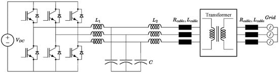
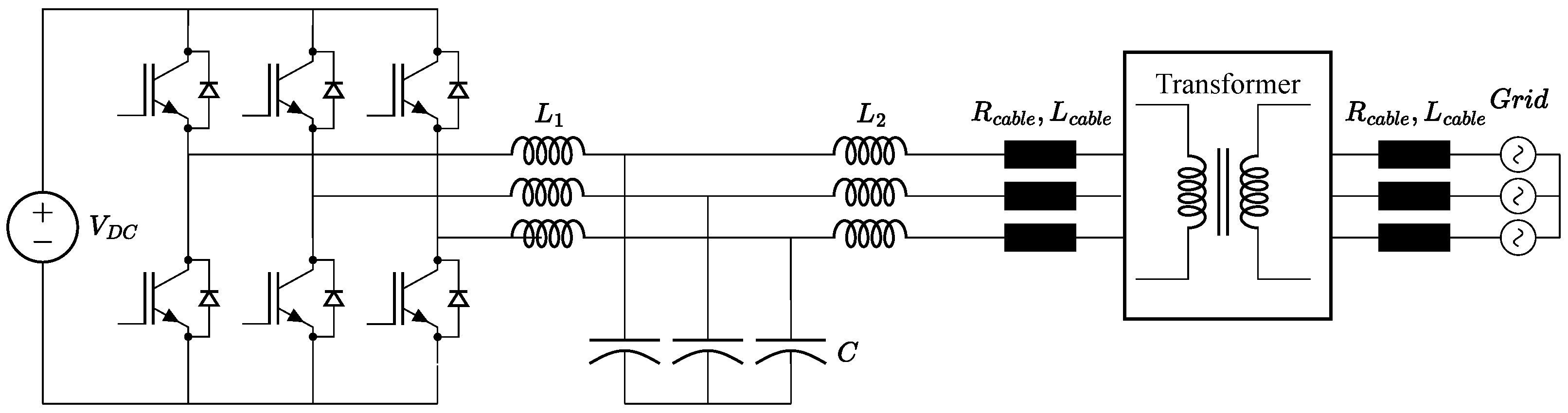
The system under study represents a typical grid-connected high-power electric vehicle charging station (EVCS), commonly adopted in fast-charging applications. In this architecture, a three-phase Voltage-Source Converter (VSC) operates as an active front-end, enabling bidirectional power exchange between the electric vehicle battery (DC link) and the utility grid [16,23]. The complete system configuration is illustrated in Figure 1.
Figure 1.
Grid-connected inverter with LCL filter.
2.1. System Configuration
The charging station interfaces on the DC side with an 800 V DC link representing the electric vehicle battery system. The DC link is connected to a three-phase Voltage-Source Converter (VSC) operating as a controlled AC/DC conversion stage. The VSC is implemented as a three-phase PWM converter, typically based on a two-level topology, although multi-level solutions are increasingly adopted in high-power applications [24,25]. Operating as an active front end, the converter enables bidirectional power exchange between the DC link and the utility grid, supporting both grid-to-vehicle (G2V) and vehicle-to-grid (V2G) modes [16,26].
The AC output of the VSC is connected to the kV low-voltage (LV) system through a three-phase LCL filter, which provides effective attenuation of high-frequency switching harmonics while preserving fast dynamic response and compliance with grid harmonic limits [23]. The filtered LV output is then conveyed to the transformer through short-length three-phase AC cables representative of a local installation.
The LV side feeds a 315 kVA Dyn11 distribution transformer, which steps the voltage up from kV to 22 kV for medium-voltage (MV) grid interfacing. The Dyn11 configuration (delta-connected MV side and grounded wye LV side) provides galvanic isolation, introduces a 30° phase shift, blocks zero-sequence harmonics, and ensures a stable LV neutral. The transformer rating provides sufficient margin for the converter operating power of approximately 300 kW.
On the MV side, the transformer is connected to the utility grid through a 1 km long 22 kV feeder. The electrical parameters of the LV and MV cables are detailed in Section 2.2.
2.2. Cable Parameters
On the low-voltage side, the connection between the VSC (at the output of the LCL filter) and the transformer LV windings is realized through short-length AC cables representative of a local installation within the charging station. Each phase employs a three-core 240 mm2 copper cable, rated for approximately 460 A continuous current after derating, which safely accommodates the converter full-load current of about 455 A. According to the Nexans datasheet (IEC 60502-2 compliant), a 3 × 240 mm2 copper cable installed in free air at 30 °C has a nominal ampacity of approximately 553 A, providing adequate thermal margin [27]. The selected LV cable also offers a short-circuit withstand capability of approximately kA for 1 s, in line with IEC thermal limits for a 240 mm2 conductor [27].
On the medium-voltage side, the transformer is connected to the utility grid through a 1 km long 22 kV feeder implemented using a three-core 240 mm2 XLPE-insulated copper cable, selected in accordance with IEC 60502-2 standards [27,28]. The MV cable sizing is governed primarily by voltage-drop constraints and short-circuit withstand capability, as the nominal current at 315 kVA and 22 kV is only ∼8.3 A. The selected conductor cross-section ensures compliance with typical distribution voltage-drop limits (approximately 5%) and provides sufficient thermal capacity to withstand fault currents of approximately kA for 1 s. According to manufacturer data, the per-kilometer impedance of the MV cable at 50 Hz is characterized by an AC resistance of /km and an inductive reactance of approximately /km, corresponding to an inductance of about mH/km [27]. These parameters are included in the simulation model to accurately represent line losses, voltage drop, and the contribution of the MV feeder to system impedance and resonance behavior.
3. Modeling of Converter and Control System
Converter control and protection are implemented using voltage and current measurements taken on both sides of the LCL filter. Three-phase voltage sensors at the point of common coupling (PCC), corresponding to the kV bus on the grid side of the LCL filter, provide the grid voltage feedback (). These signals are processed by a Phase-Locked Loop (PLL) for grid synchronization, yielding the grid angle and frequency reference [29]. Using this reference, measured three-phase voltages and currents are transformed into the synchronous reference frame.
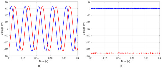
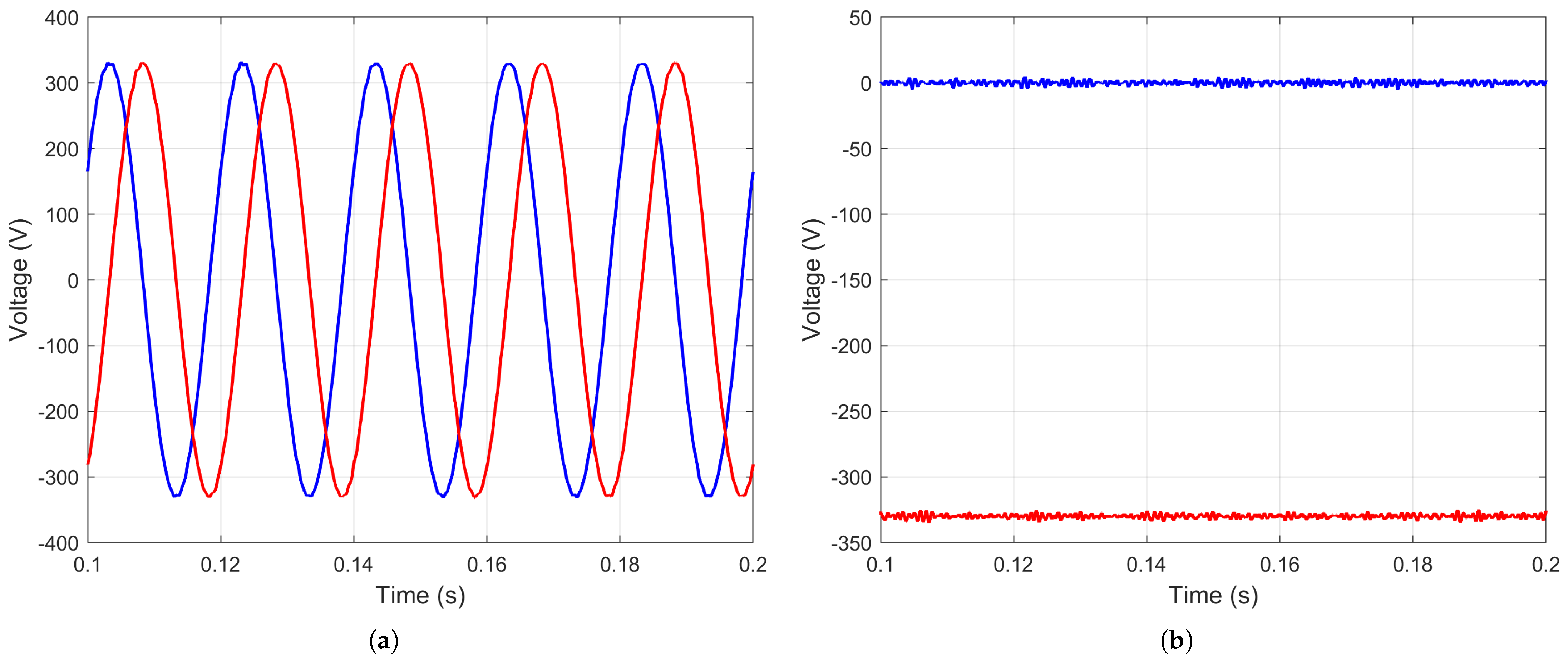
In the frame, the fundamental components of voltages and currents appear as DC quantities under steady-state conditions, enabling the use of linear proportional–integral (PI) controllers with reduced complexity and improved robustness compared to stationary reference-frame control [29]. The transformation yields the grid-voltage components and and the corresponding current components and , as illustrated in Figure 2. The current components constitute the main control variables: regulates active power exchange and the DC-link voltage, while controls reactive power and power factor. The inner current control loop is implemented using inverter-side current measurements (), allowing direct actuation by the VSC switching and avoiding additional phase delay and noise associated with grid-side measurements.
Figure 2.
Grid-side quantities for a 100 kVA inverter: (a) Grid-side voltage components on the axes (red) and (blue); (b) Grid-side voltage (red) and (blue).
In synchronous-frame (voltage-oriented) control, reference values and are imposed by higher-level control loops. In this study, is set to zero to ensure unity power factor operation, while is determined to achieve the desired active power transfer between the DC link and the grid [16]. Under this strategy, the grid-side current is indirectly regulated to be in phase with the grid voltage and to match the commanded magnitude. Grid-side current measurements () are used for monitoring purposes and can be exploited for outer-loop control or active damping of the LCL filter resonance. The availability of both inverter- and grid-side current feedback enables the implementation of active damping strategies, if required, to enhance system stability.
Overall, the PLL-synchronized -frame current control ensures stable DC-link regulation, compliance with grid-code requirements (harmonic distortion and power factor), and robust operation under varying grid conditions [16,29].
3.1. Current-Mode vs. Voltage-Mode Control
Grid-connected converters can regulate power flow using either voltage-mode control or current-mode control. In a voltage-mode scheme, the converter’s AC terminal voltage magnitude and phase are directly controlled to adjust real and reactive power output [29]. While structurally simpler, voltage control lacks a current feedback loop, limiting its ability to actively regulate the converter’s output current. As a result, a voltage-controlled converter is not inherently protected against overcurrents, and rapid changes in power commands or grid faults can drive the current to excessive levels.
In contrast, current-mode control incorporates an inner current regulation loop, tightly regulating converter output current via high-bandwidth feedback. This enables real-time power control, inherent overcurrent protection, and fast dynamic response [29,30]. Furthermore, in the rotating reference frame, the control signals become DC quantities under steady-state conditions, enabling the use of low-order PI regulators with zero steady-state error [31].
The averaged dynamic model of a VSC connected to the grid through an inductive interface can be expressed in the reference frame as [29]:
where , are the converter currents, , are grid voltages, and , are converter voltages in the frame. The converter voltages relate to the modulation indices and via:
To eliminate cross-coupling introduced by the L terms, decoupling is achieved by redefining the modulation signals [29]:
Substituting Equations (5) and (6) into (1) and (2) yields two decoupled, first-order dynamics:
where and are the new decoupled control inputs, which independently regulate the and current components, respectively. This decoupling eliminates the cross-coupling effects introduced by the terms and simplifies the system dynamics into two first-order linear equations.
3.2. PI Controller Design and Closed-Loop Response
Given the decoupled first-order dynamics in each axis, simple proportional–integral (PI) controllers are employed to regulate and to their reference values . In the synchronous frame, the current references are DC (constant) under steady-state conditions, so that a PI compensator can track the reference with zero steady-state error. This is a major advantage of -frame control: unlike an (stationary frame) controller, where the compensator must handle oscillatory 50/60 Hz error signals (often requiring high-order or resonant controllers), in the rotating frame the error is a DC quantity that a PI regulator can easily drive to zero. The block diagram of the considered controller is shown in Figure 3.
Figure 3.
Simplified block diagram of controller.
The decoupled dynamics (7) and (8) allow simple PI controllers to be used in each axis. For the d-axis, a PI controller is applied of the form:
and similarly for .
Choosing
leads to a closed-loop transfer function as follows:
with a time constant .
This first-order response ensures that tracks and tracks with minimal delay. In our system, the switching frequency is 10 kHz, and we select a control bandwidth of 1 kHz (i.e., ms), as per best practices in the literature [30,31]. This choice provides a fast current response while maintaining a sufficient margin below the frequency of the PWM sampling and away from the resonance frequecy of LCL filter.
4. LCL Filter Design
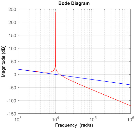
A straightforward interface solution for grid-connected converters is a single series inductance per phase (L filter) [21]. However, its first-order attenuation (−20 dB/dec) is generally insufficient to meet stringent harmonic limits without resorting to excessively large inductance values. In particular, IEEE Std. 519 imposes individual current harmonic limits down to % of the fundamental in the 35th–50th harmonic range [17], requiring strong attenuation already around 1.75 kHz to 2.5 kHz. Under conservative assumptions (e.g., inverter harmonic voltage magnitude p.u. and allowable current p.u.), the required inductive reactance scales as p.u., leading to impractically large inductors. Such a solution also causes excessive fundamental voltage drop (), degrades current-control dynamics, and results in increased size, losses, and cost. The limited attenuation capability of an L filter compared to an LCL solution is illustrated by the frequency responses shown in Figure 4.
Figure 4.
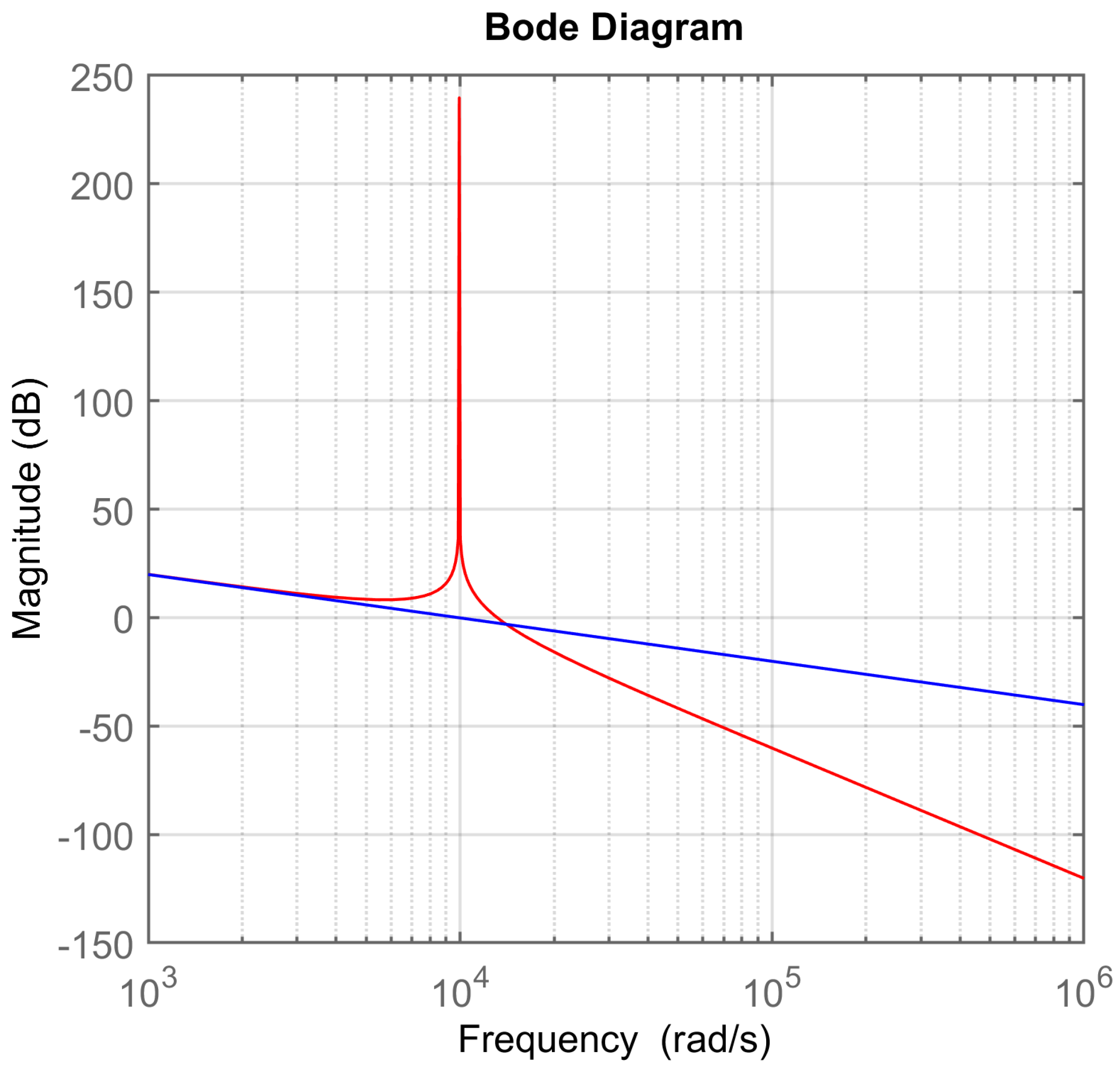
Bode plot comparison between an L filter (blue) and an ideal undamped LCL filter (red).
Compared to an L filter, an LCL topology achieves the required high-frequency attenuation with a much smaller total inductance at the expense of introducing a resonance that must be properly placed and damped. For this reason, LCL filters are widely adopted in high-power grid-connected converters.
The design procedure presented in this section targets a three-phase PWM voltage-source converter operating at 10 kHz, representative of consolidated implementations within the 5 kHz to 30 kHz range. The filter is sized to ensure compliance with IEEE Std. 519 harmonic limits, limit reactive power absorption and fundamental voltage drop, and guarantee adequate attenuation at the switching frequency.
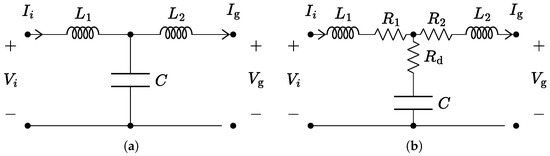
For design and frequency-domain analysis, the three-phase LCL filter is represented by its single-phase equivalent circuit, shown in Figure 5a, which forms the basis for the analytical derivations and step-by-step sizing procedure described below.
Figure 5.
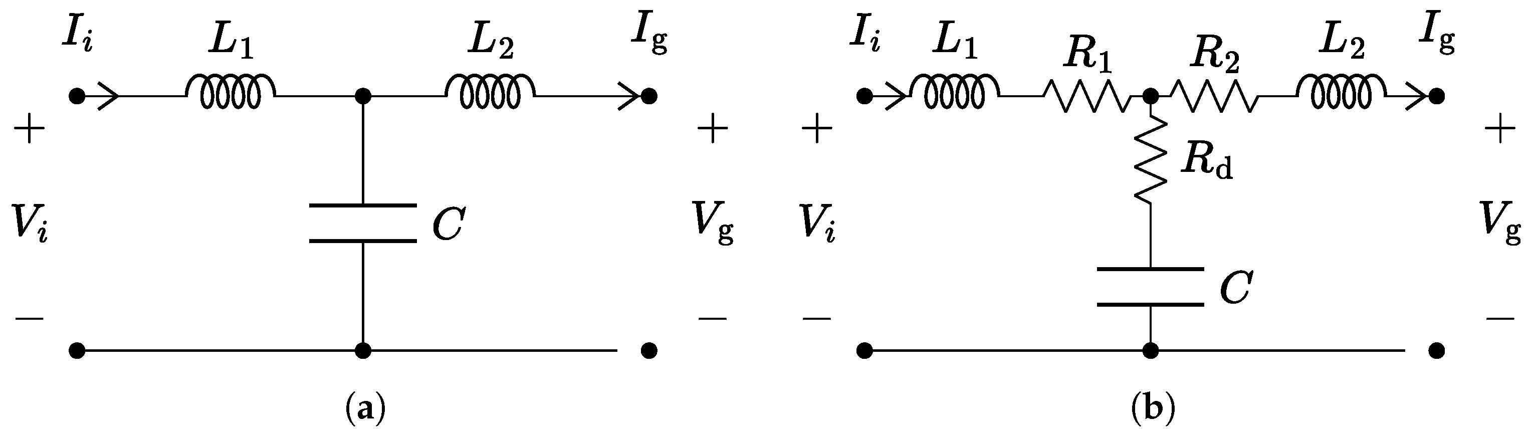
Single-phase equivalent of (a) the ideal and (b) the non-ideal LCL filter with damping resistor .
Single-Phase Equivalent and Transfer Functions
The single-phase equivalent consists of an inverter-side inductor , a grid-side inductor , and a shunt capacitor C (Y-connected in the three-phase implementation). The LCL filter introduces a resonance at
which must be placed between the fundamental frequency and the switching frequency and adequately damped to avoid amplification around .
Assuming the grid behaves as a stiff voltage source for harmonic and switching-frequency components, the grid-side voltage can be neglected in the small-signal transfer from inverter voltage to injected current . Under this assumption, the ideal (lossless) transfer function in (14) exhibits a dB/dec roll-off beyond resonance, providing strong attenuation at the switching frequency, as also highlighted by the ideal LCL response in Figure 4.
In practice, damping is required to suppress the resonant peak observed in the ideal LCL response. A common passive solution is a series damping resistor in the capacitor branch, as shown in Figure 5b.
Including the damping resistor, the transfer function becomes
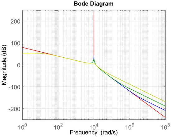
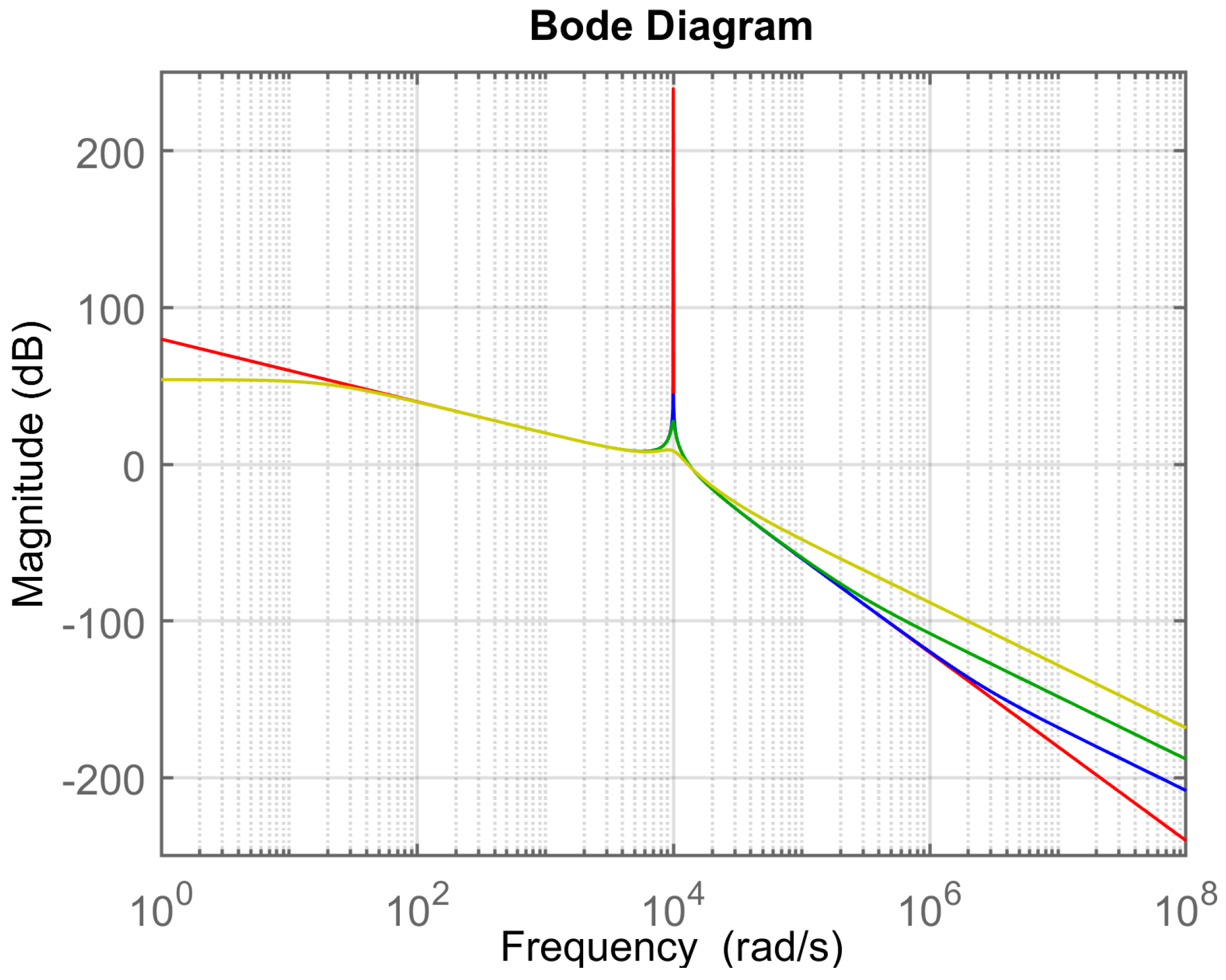
where and denote the inductor winding resistances. The effect of different damping resistance values on the resonance peak and high-frequency attenuation is illustrated in Figure 6.
Figure 6.
Bode plot of the LCL transfer function for different damping resistances: (red), (blue), (green), and (yellow).
The analytical framework established above forms the basis for the step-by-step LCL filter design procedure presented in the following subsection.
5. Step-by-Step Design Procedure
The following design steps are used to determine the LCL filter parameters for the grid-connected EV charger application. We aim to satisfy harmonic attenuation requirements (IEEE Std. 519) while minimizing filter size and ensuring stable, efficient operation.
5.1. STEP 1: Capacitance Selection Based on Reactive Power Limit
We choose the filter capacitance C such that the reactive power drawn by C at fundamental frequency is a small fraction of the converter’s rated power. This limits the VARs consumed by the filter and avoids degrading the power factor. A typical guideline is to limit the reactive power of the capacitor to about 0.5–2% of the VA rating of the converter (we can choose a corresponding upper bound as a fraction of the total rated power in the range of 0.05 to 0.2 p.u.). In equation form,
where Hz is the grid frequency, is the phase voltage (RMS) of the AC source, and is the rated power per phase (e.g., kVA for a 100 kVA 3-phase charger).
Larger (e.g., 0.1 or 0.2) would allow a bigger C (stronger filtering) but at the expense of more reactive current. In practice, we choose C near the upper limit that is acceptable, in order to maximize high-frequency filtering capability without exceeding (for example) 20% VAR draw at no-load. Let us select C such that (20% criterion) for this design.
5.2. STEP 2: Resonant Frequency Placement
We select the LCL filter’s resonant frequency to be well below the inverter switching frequency but well above the grid frequency. A common rule is
ensuring the resonance is at least one decade above 50 Hz (so it is not excited by any low-order harmonics of grid or converter) and sufficiently below the Nyquist frequency of the PWM (to allow adequate attenuation at ). Another approach is to choose as the geometric mean between the edge of the passband and the start of the stopband (e.g., between and ):
where may be chosen as 500 Hz (allowing harmonics up to the 10th) and (half of ), which yields .
5.3. STEP 3: Minimum Inductance for Harmonic Attenuation
For effective harmonic attenuation, while maintaining component sizing practical, the total filter inductance must be carefully bounded between a lower and upper limit and , respectively:
5.3.1. Choice of
As first, the choice of is addressed. Specifically, by defining
- the harmonic attenuation constraint,
- the resonance frequency constraint
is chosen as the upper bound of the two:
is determined ensuring the compliance with harmonic emission limits, particularly in the supraharmonic range where IEEE Std. 519 [17] does not explicitly prescribe limits beyond the 50th harmonic. The design conservatively assumes the use of 35th–50th harmonic limits (i.e., ). According to the IEEE Std. 519, the current distortion for such high-order harmonics should not exceed 0.3% of the rated fundamental current. This sets the limits for the grid current at the switching frequency. The inverter output voltage at the switching frequency before the filter is selected as 0.3 p.u. based on the FFT results (see Section 6). The frequency-domain transfer function is obtained from (14) for an ideal LCL filter without damping as
Substituting , where is the dominant harmonic frequency (typically the switching frequency), and rearranging, we derive the expression for the minimum total inductance required to ensure the high-frequency harmonic currents remain under the IEEE limits:
where
Substituting the values into (23), we get
This value ensures that the dominant switching harmonic (10 kHz switching and its side bands) does not cause excessive current injection into the grid. It also highlights that a basic L filter would demand an impractically large inductance to meet the same attenuation, justifying the need for an LCL topology.
is then determined assuming . The reason is explained in Appendix A. In this assumption, from the resonance frequency expression (13), we get
from which
Using Hz from Step 2 and F from Step 1,
This value becomes one of the bounding conditions for inductance selection. If computed earlier is less than this value, then will govern the filter design.
5.3.2. Choice of
While an LCL filter requires sufficient inductance to effectively attenuate high-frequency switching harmonics, an excessive inductance value can lead to undesirable voltage drops at the fundamental frequency. This not only increases reactive power consumption but also necessitates a higher DC-link voltage to compensate for the voltage drop across the inductors. Therefore, a trade-off must be made to balance harmonic attenuation, voltage drop, and system cost. The inverter output voltage must then satisfy one of the two following DC bus voltage requirements [29]:
To limit the voltage drop across the filter inductors , a typical design guideline restricts the drop to no more than 5–10% of the RMS grid voltage at full load. However, to reduce control complexity and preserve dynamic margin, some designs allow a drop up to 20%. This upper bound also accommodates scenarios with reactive power delivery, where voltage drop is in phase with grid voltage (worst case scenario), requiring more margin in the inverter-side voltage (). When delivering real power at unity power factor, the inductor voltage drop is orthogonal to the grid voltage [32]. The inverter voltage magnitude becomes
where is the RMS phase voltage (assumed ), , and is the rated phase current. Based on this maximum allowable voltage drop, the resulting inverter terminal voltage is approximately
If reactive power delivery is required, the voltage drop would be in phase with the grid voltage, leading to
Assuming (28), it holds
which significantly increases system cost and stress. Therefore, constraining the inductor voltage drop to 0.2 p.u. not only improves efficiency but also keeps requirements practical. This implies that excessive voltage drop across inductors increases , and hence . To cap the voltage drop across at 20% of the phase voltage magnitude for this paper, the total impedance should satisfy the following:
Solving for , it finally gives
Substituting the values
- (phase RMS voltage),
- ,
- (for 100 kW at unity power factor), in (35) .
The final filter inductance value must then satisfy
In our case, considering a 100 kW power transfer, the values calculated for and yield the practical bound:
With this approach, the design maintains resonance within bounds, ensures adequate harmonic attenuation, and keeps the reactive current drawn by the filter within acceptable limits.
Larger filter inductance L improves harmonic attenuation and reduces high-frequency ripple (see Appendix A), but at a significant cost. At high power levels, inductors are bulky, lossy, and expensive due to saturation limits, winding complexity, and thermal constraints, whereas capacitors are more compact and significantly cheaper per unit of reactive power (kVAR). In practical designs, the cost per kVAR of inductors is typically 3–4 times higher than that of capacitors. Moreover, increasing L negatively affects system dynamics by reducing the achievable control bandwidth. For these reasons, the preferred design strategy is to minimize the inductance while maximizing the filter capacitance within reactive power and stability limits. This trade-off leads to a compact, cost-effective filter design and motivates the symmetric configuration . Based on the analytical constraints derived above, an initial LCL filter configuration is selected with and , representing the minimum feasible inductance that satisfies attenuation and stability requirements.
Time-domain simulations are then performed to evaluate THD and individual current harmonics at the PCC. If IEEE Std. 519 limits are not met, the inductance values are progressively increased (maintaining ) up to . The impact of inductance variation on harmonic performance is analyzed and discussed in the following section.
5.4. STEP 4: PI Tuning and Reference Values for Controller
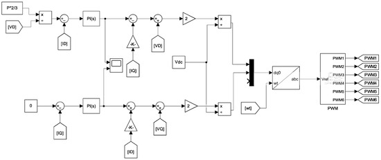
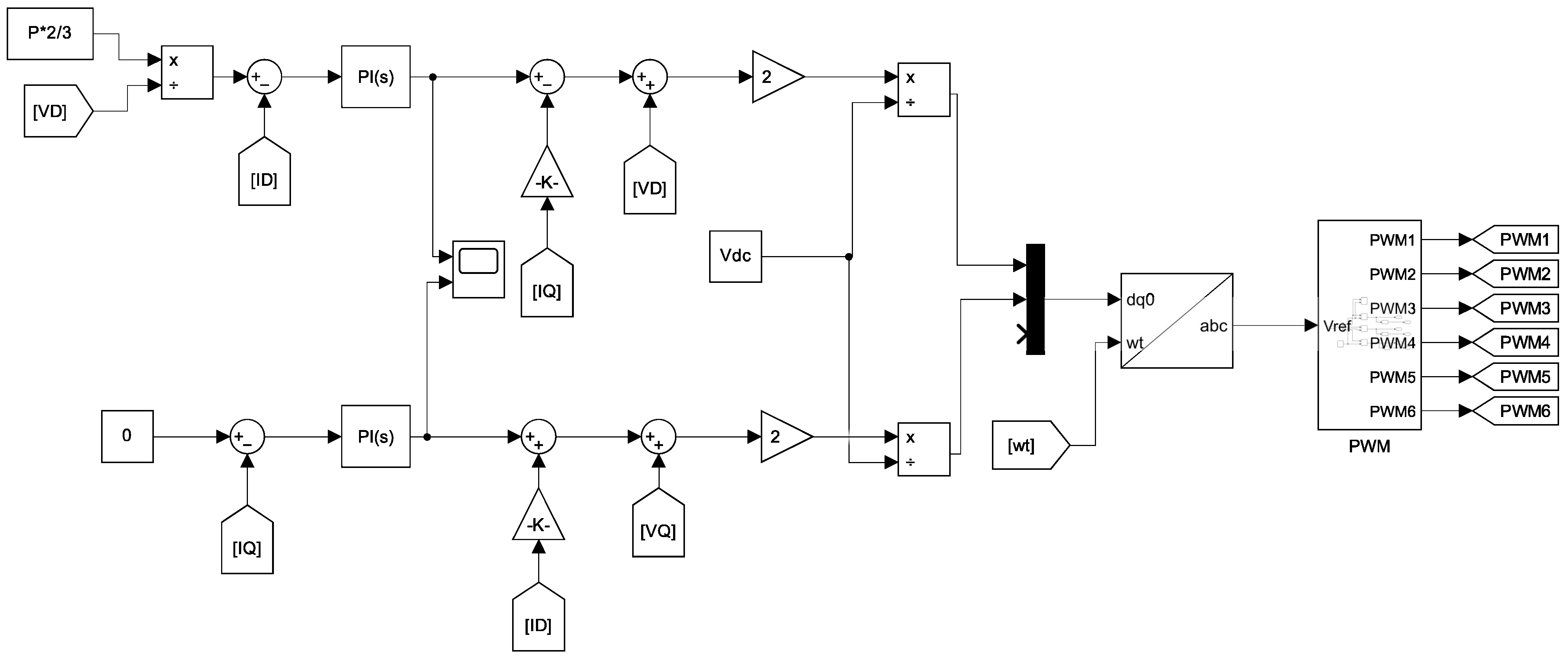
With the filter parameters finalized, the next step is to design the inner current control loops in the synchronous dq-reference frame. We adopt a standard decoupled current control approach as described in Yazdani et al. [29], which regulates the converter dq-axis currents (, ) by means of the modulation of the inverter output voltages (the overall block diagram is shown in Figure 7).
Figure 7.
Current controller in Simulink.
The d-axis is aligned with the grid voltage vector (, ), thereby decoupling the control of active and reactive powers. Under this configuration, the real and reactive power at the point of common coupling (PCC) are given as:
which, at steady state with , simplifies to
Hence, controlling regulates real power flow and DC-link voltage, while governs reactive power exchange with the grid. Hence, controlling regulates real power flow and DC-link voltage, while governs reactive power exchange with the grid. In this study, the reference for the quadrature-axis current is set as , ensuring that the inverter does not exchange reactive power with the grid. The q-axis voltage is also maintained at 0 through the PLL, providing the reference angle for Park transformation. The direct-axis current reference is computed to deliver a constant active power P to the grid, and is given by
where P is the injected active power (100 kW in this case), and is the d-axis component of the grid voltage obtained via a Park transformation from the measured three-phase voltages. The transformation process involves a two-step conversion: a transformation from abc frame to which are known as Clarke components followed by a to using a phase-locked loop (PLL) for angle tracking to convert Clarke components to Park components.
In Simulink implementation, can be generated either by directly using a constant value of 205 A (computed as , considering as obtained from Figure 2b) or dynamically via a computation block, where the power reference (100 kW) is multiplied by gain and divided by the real-time measured quantity using a product block. This allows for adaptive current control under varying grid voltage conditions. We employ proportional-integral (PI) controllers for both and current loops. These controllers are designed to be significantly faster than the outer voltage or power control loops and the grid frequency (50 Hz), and 10 times lower than the switching frequency, as explained in Section 3.2. The control time constant is selected as 1 ms. Using Equations (10) and (11), we obtain the following values:
where , and . For our system, with , we obtain
Assuming and inverter switch on-state resistance , we have
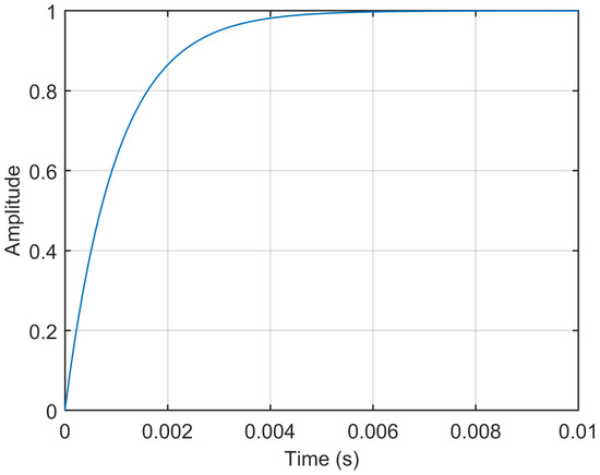
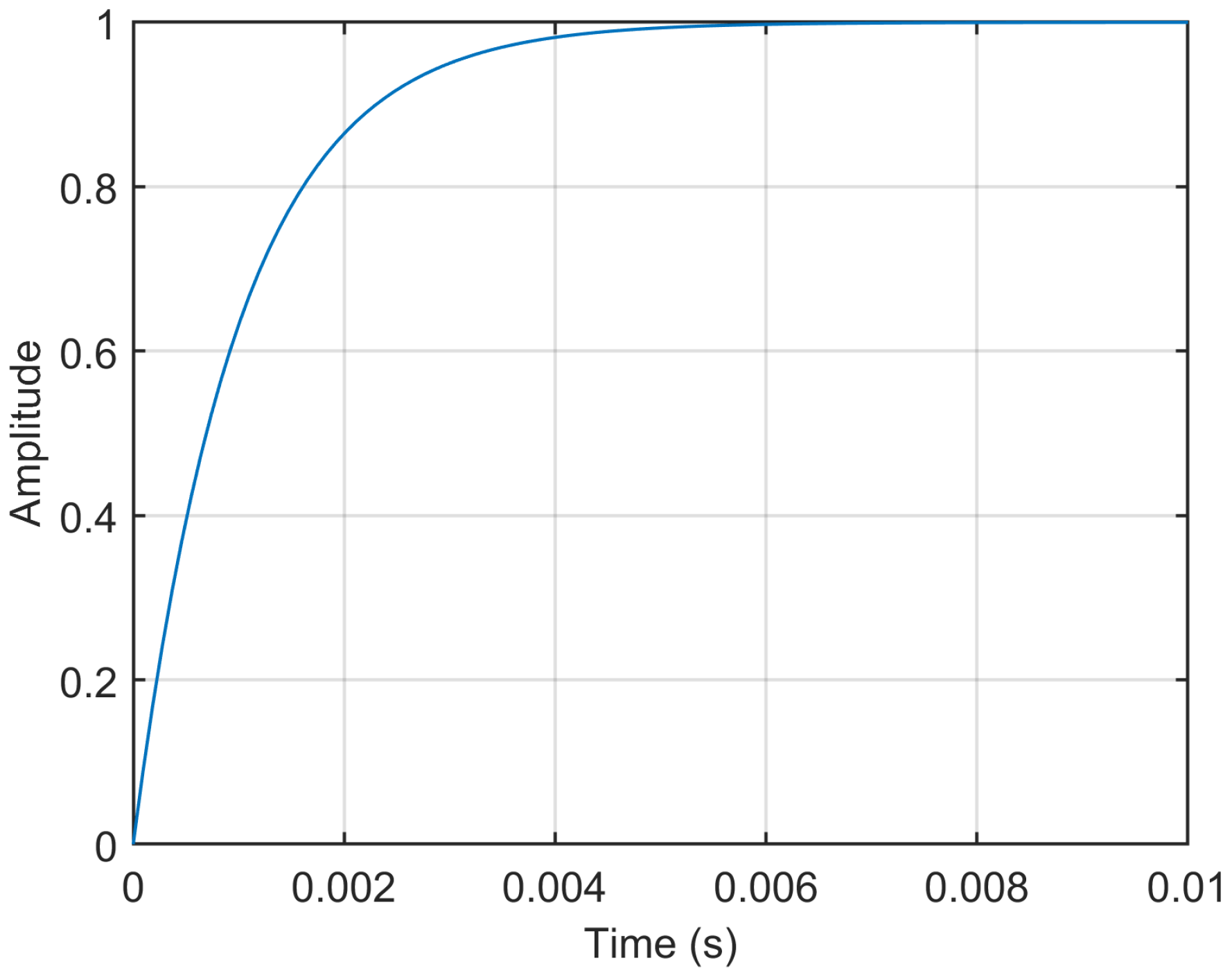
These parameters yield fast and stable current regulation while maintaining decoupling between the d and q axes. The values of will change based on the inductance value selected. To validate the dynamic performance of the designed controller, the step response of the closed-loop system was analyzed. As illustrated in Figure 8, the system exhibits the characteristics of a first-order response, including a smooth rise and no observable overshoot. This confirms the expected performance of the controller, indicating sufficient damping and stability for the intended application.
Figure 8.
Step response of the inner closed-loop controller.
With all control variables and filter parameters defined, the converter system is ready for simulation. Results including THD and harmonic performance for different inductance values are discussed in the next section.
6. Results: Verification of the Designed LCL Filter on Simulated Cases
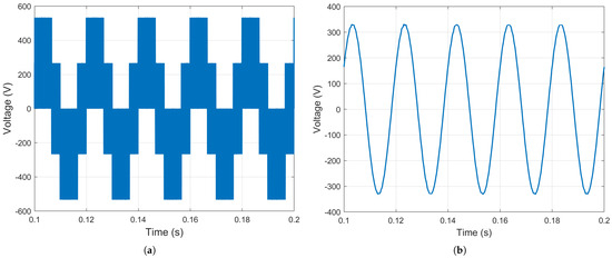
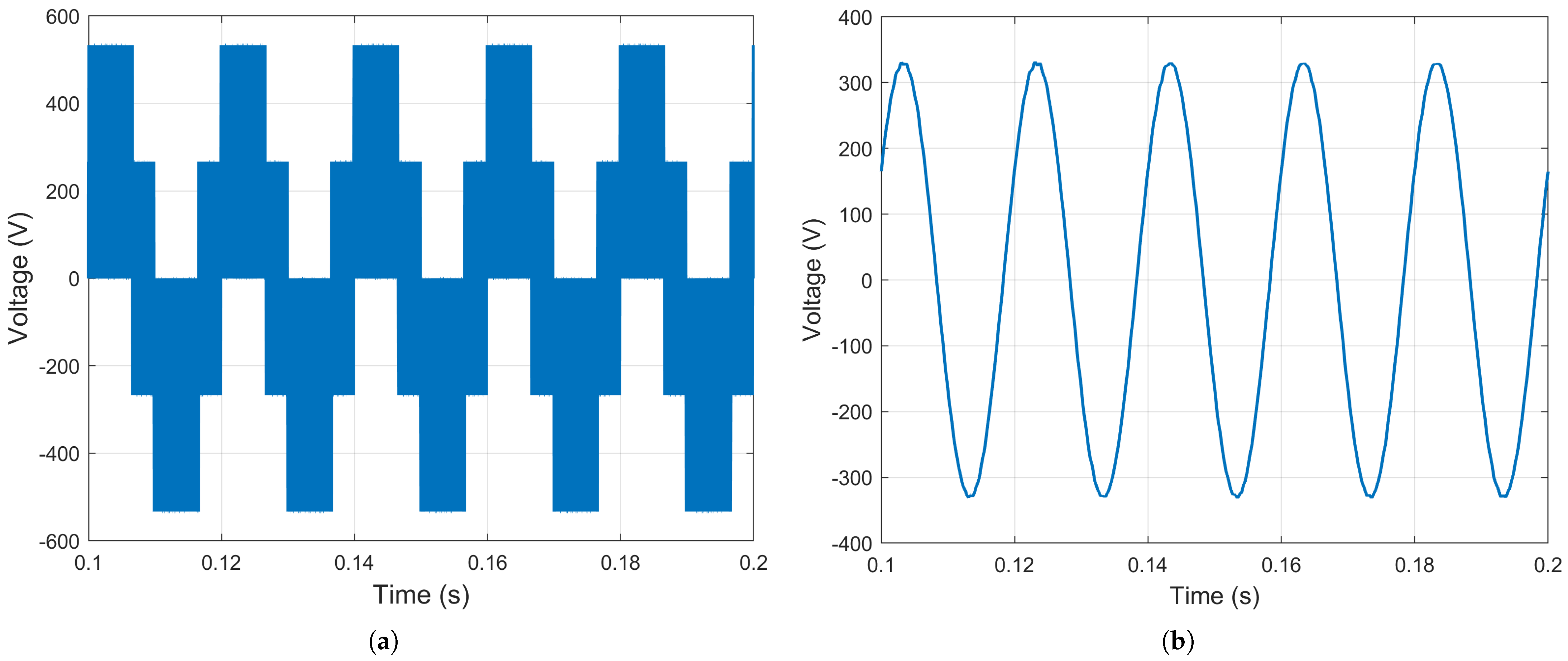
For the initial test, both filter inductors were set to the minimum acceptable values () to evaluate a worst case harmonic scenario. Figure 9a shows the line voltage waveform at the inverter output before filtering, which is visibly distorted by high-frequency ripple. The corresponding FFT spectrum (see Figure 10a) indicates that the dominant harmonic at the switching frequency in the inverter voltage is about 0.3 p.u. (approximately 30% of the fundamental amplitude). After the LCL filter, the output voltage waveform (Figure 9b) is nearly a perfect sinusoid. Virtually all switching by-products are removed (see Figure 10b) and the filtered voltage harmonics are well within the recommended limits of the IEEE Std. 519 for systems ≤ 1 kV (individual harmonic voltages < 5% of the fundamental, THD < 8%).
Figure 9.
Inverter Output Voltage before and after LCL filter for : (a) Output Voltage before filter; (b) Output Voltage after filter.
Figure 10.
Harmonic Spectrum of Inverter Output Voltage before and after LCL filter for : (a) Output Voltage before filter; (b) Output Voltage after filter.
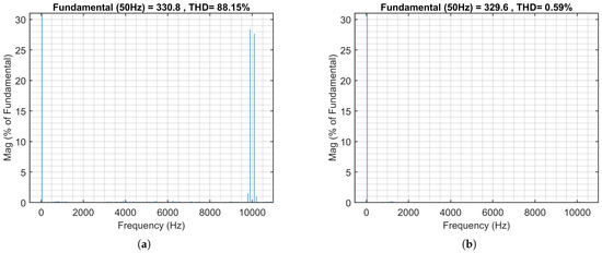
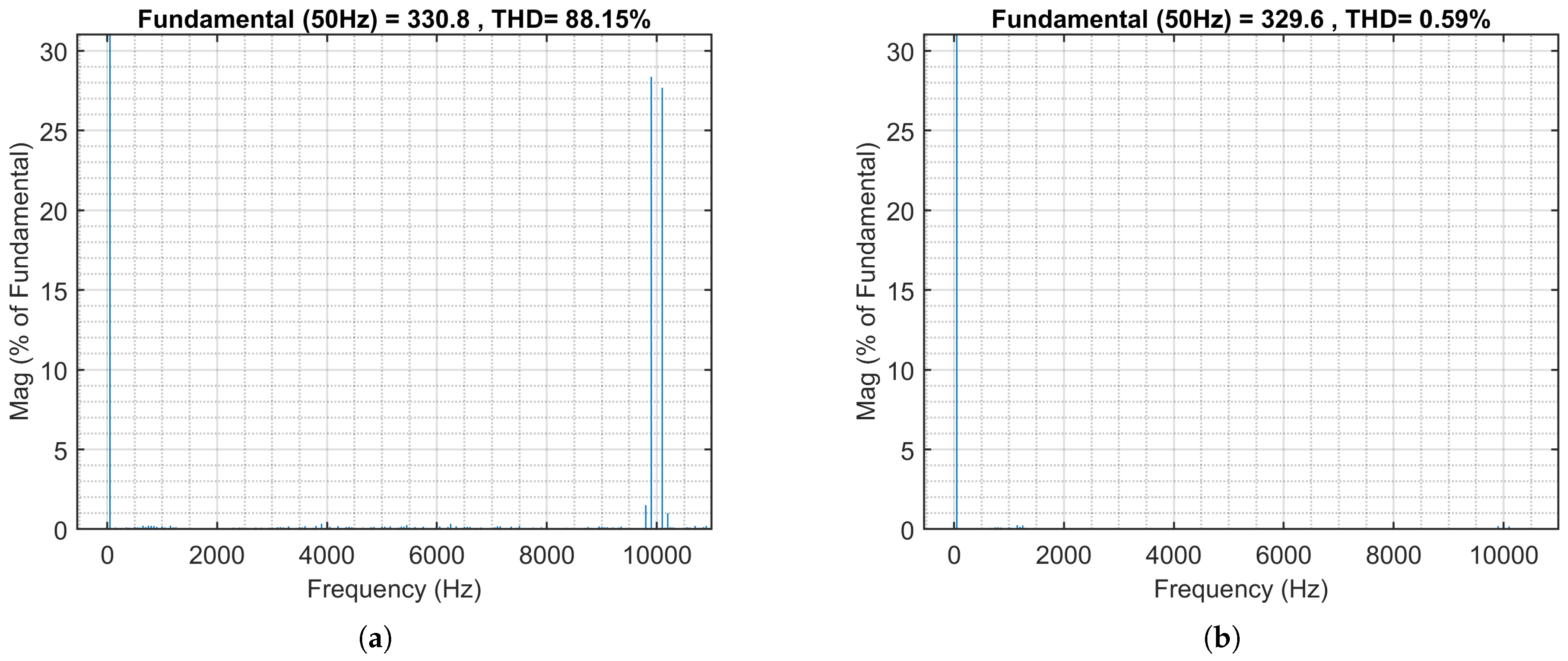
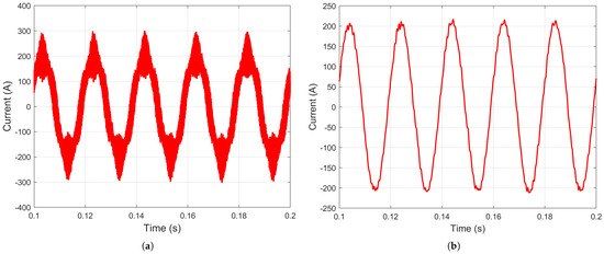
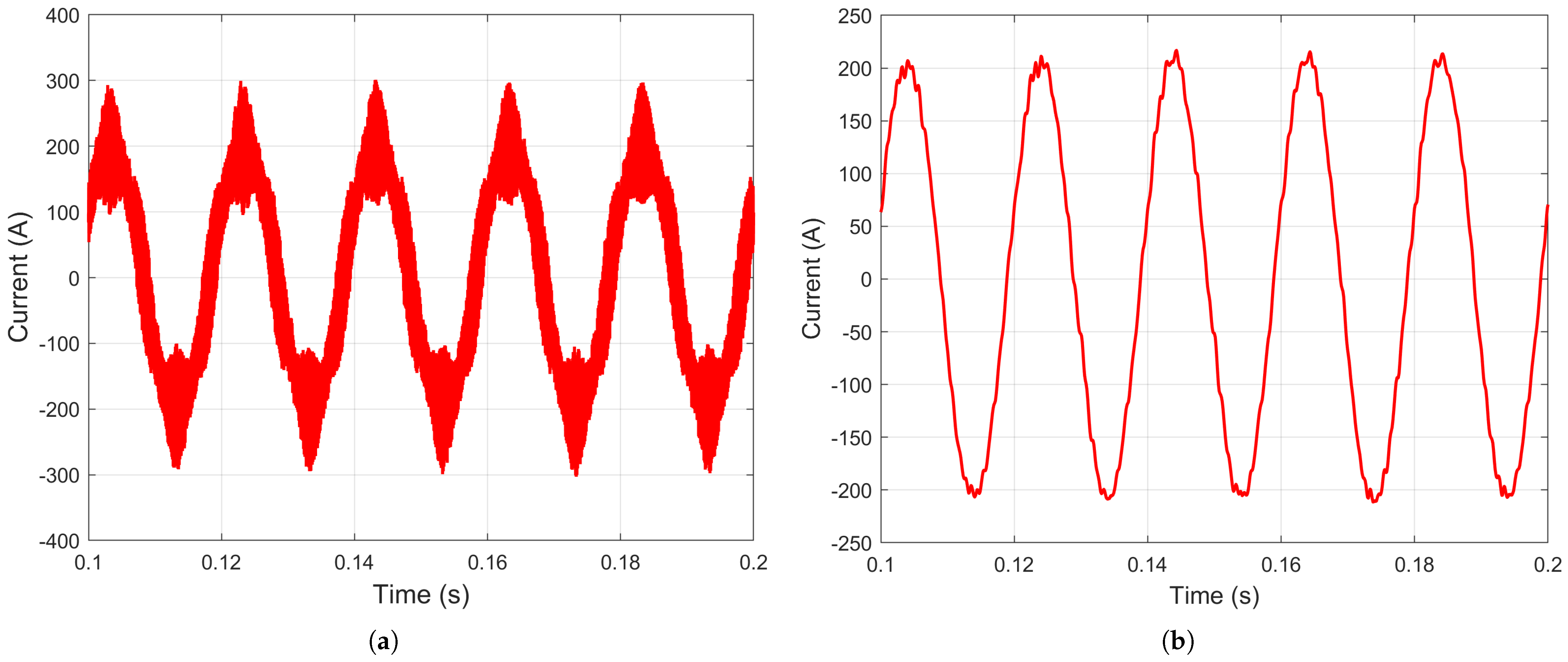
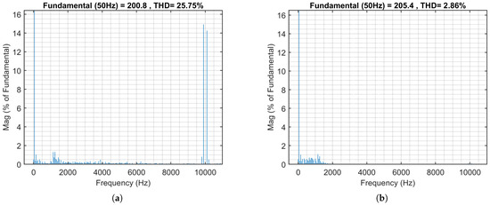
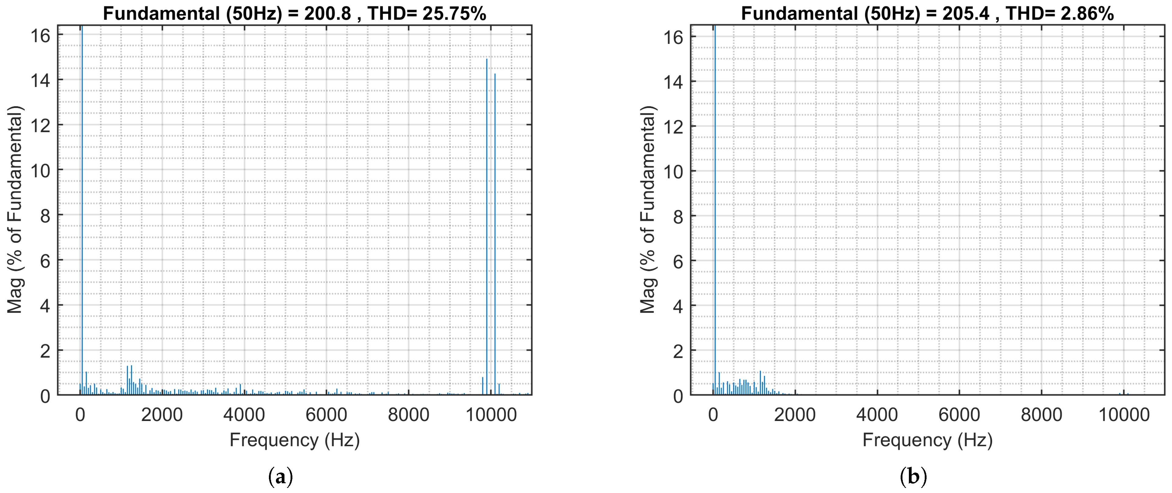
Similarly, the inverter-side current before filtering contains significant high-frequency distortion due to the PWM switching. As shown in Figure 11a, the inverter current waveform is superimposed with noticeable oscillations at the switching frequency. Its harmonic spectrum (see Figure 12a) reveals a prominent component at the sideband harmonics of switching harmonics. After the LCL filter, the grid-side current (Figure 11a) is almost purely sinusoidal, with the switching ripple almost completely eliminated. The harmonic current distortion (Figure 11b) is drastically reduced from the unfiltered case to below 0.1% with the filter in place. It is noteworthy that when the switching frequency of the PWM inverter could be slightly detuned to kHz (corresponding to the 195th harmonic of 50 Hz) instead of an exact 10 kHz (200th harmonic), the dominant harmonic orders are 193 and 197. This could be achieved to avoid falling under the stricter limits often imposed on even-order harmonics, thereby simplifying compliance while still being effectively attenuated by the filter.
Figure 11.
Inverter Output Current before and after LCL filter for : (a) Output Current before filter; (b) Output Current after filter.
Figure 12.
Harmonic Spectrum of Inverter Output Voltage before and after LCL filter for : (a) Output Current before filter; (b) Output Current after filter.
Because the LCL filter is designed to target high-frequency harmonics, it has minimal impact on lower-order harmonics (those below about 500 Hz). In practice, however, the inverter’s control system kept these low-frequency harmonics very small. All individual harmonic components in the 50–500 Hz range remained well within the IEEE Std. 519 limits even without significant filter attenuation at those frequencies. In other words, no appreciable low-order distortion was present in the output waveforms, and the filter’s primary role was indeed the reduction in switching (high-order) harmonics.
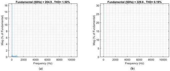
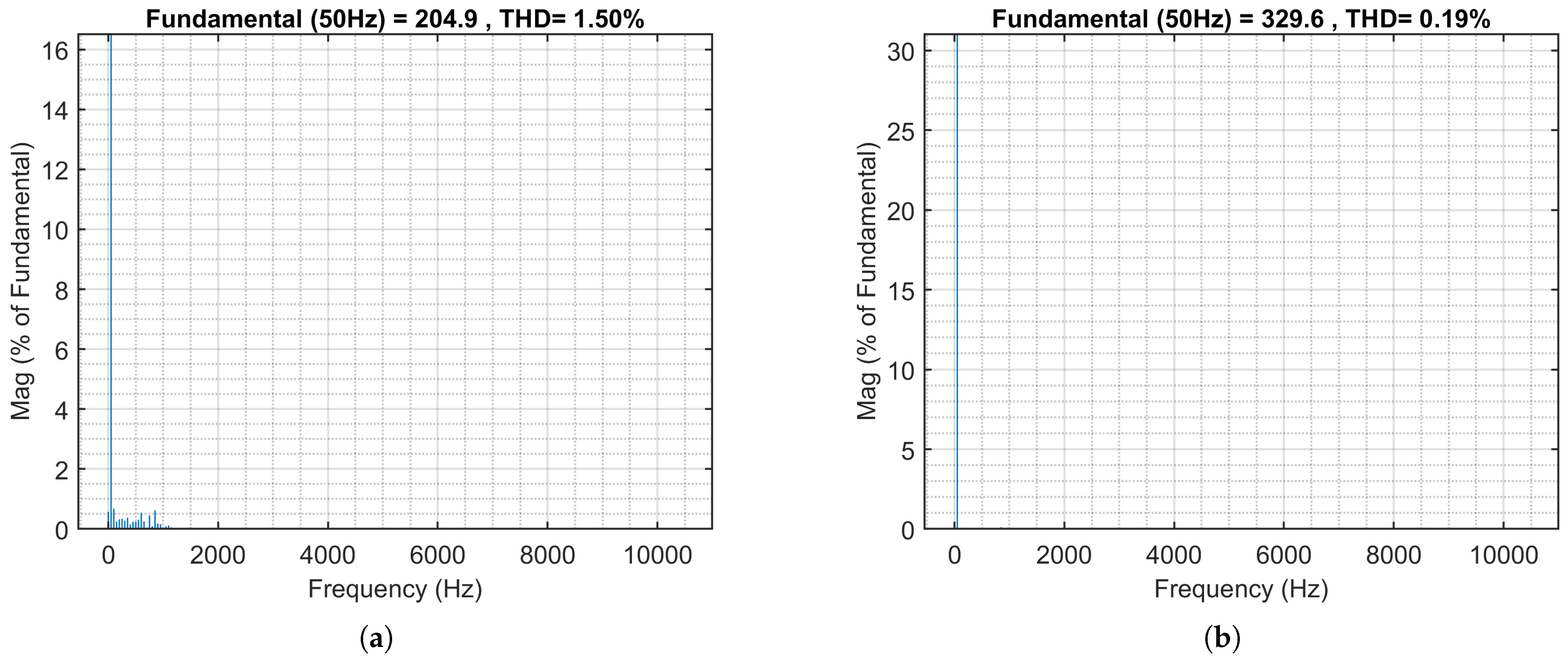
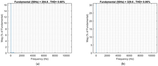
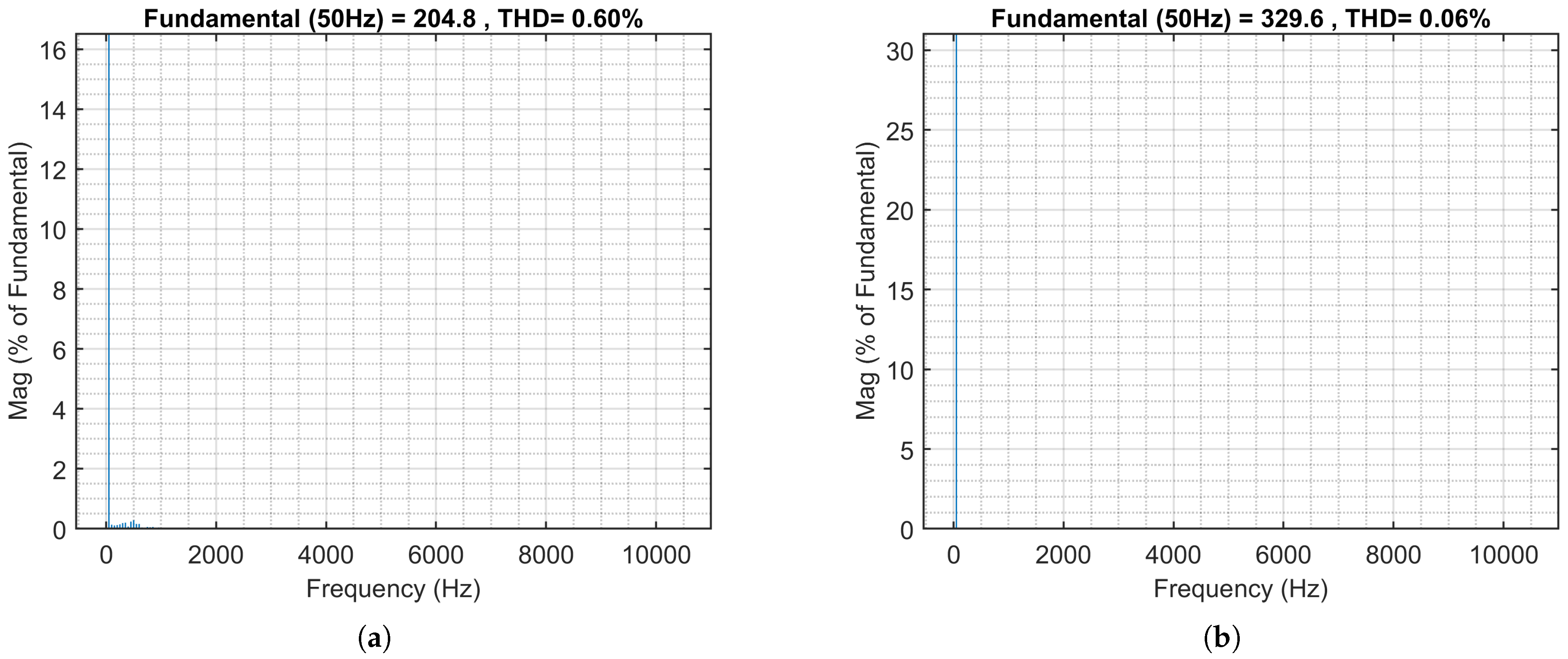
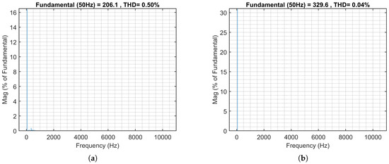
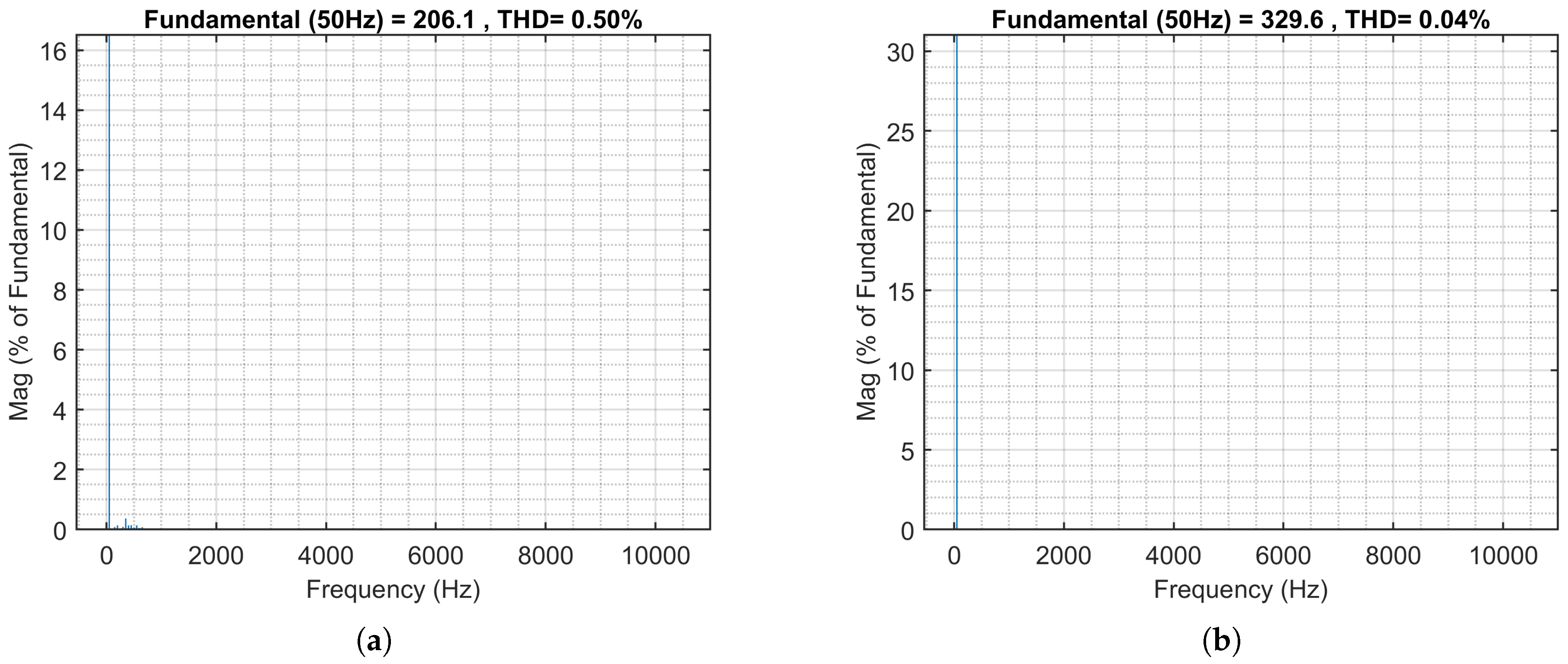
Increasing LCL filter inductance values beyond the minimum values further improves harmonic performance (refer to Figure 13, Figure 14 and Figure 15, where inductance is increased to 3, 6 and 10 times of the minimum value, respectively). With larger inductors (approaching the maximum design inductance ), the filter cutoff frequency is lower and its attenuation of switching harmonics is stronger. For example, when and were both set to higher values (on the order of each), the output current waveform became even smoother and virtually indistinguishable from an ideal sinusoid. The THD of the grid current in this case dropped to a negligible level, and the switching-frequency components in the current spectrum were practically eliminated. These results confirm that while the minimal inductance design ( each) is sufficient to meet harmonic standards in normal situations of short-circuit power ratio and in general of MV side impedance, using higher inductance values provides an extra margin of harmonic reduction, resulting in extremely low distortion in the output waveforms. The relevance of the inductive elements for the attenuation of the supraharmonic components is confirmed by [33], where the observed contribution to the attenuation was 50% larger than that of the capacitor for the tested photovoltaic system.
Figure 13.
Harmonic Spectrum of Inverter Output Voltage before and after LCL filter for : (a) Output Current after filter; (b) Output Voltage after filter.
Figure 14.
Harmonic Spectrum of Inverter Output Voltage before and after LCL filter for : (a) Output Current after filter; (b) Output Voltage after filter.
Figure 15.
Harmonic Spectrum of Inverter Output Voltage before and after LCL filter for : (a) Output Current after filter; (b) Output Voltage after filter.
All simulation results presented in this section correspond to a 100 kVA grid-connected inverter. The LCL filter was designed using the systematic methodology proposed earlier, resulting in optimized parameters of and (the latter of course approximated as 400 μF for practical reasons). Controller gains were selected as and based on the design equations and damping criteria.
It is important to emphasize that the design methodology remains fully applicable to inverters of different power ratings. For example, in the case of a 300 kVA converter, the same step-by-step process was followed, with only the apparent power rating updated in the corresponding equations. This yields LCL filter parameters of and . Consequently, the proportional and integral control gains are adjusted to and , respectively. These values ensure an equivalent current controller bandwidth and maintain harmonic performance.
Thus, the proposed approach is scalable and adaptable, making it suitable for a wide range of applications in electric vehicle charging infrastructure and other grid-tied power electronic systems.
As a final check, the robustness of the LCL design was tested in the following condition: the same values of LCL filter components and controller and , obtained for the reference case (100 kVA inverter power with the MV grid set as 100 MVA of short-circuit power and 1 km of MV cable length), were used in scenarios with reduced short-circuit power and increased cable length. Results are shown in Table 1.
Table 1.
Verification of robustness and performance for different MV grid characteristics.
With the increase in the MV cable length, the current distortion reduces slightly, whereas the voltage distortion increases, as expected. The used values for and are those calculated for the 100 kVA and 300 kVA inverter power levels, and in fact they have a ratio of 3. Also, and values are calculated once for each inverter power level. All distortion values are below the limits and demonstrate that one unique standard design is able to cover a wide range of MV grid characteristics, having included also the very low short-circuit power of 50 MVA and the extreme case of 100 km MV feeder, well beyond normal MV grid characteristics. This approach is sensible, thinking that if the inverter with the LCL filter comes as a product, customization is expensive and kept to a minimum by the manufacturer: standard settings are shown to work with very pessimistic scenarios for the MV grid.
Compared with classical LCL design recipes that rely on iterative tuning, the present results contribute: (i) an explicit, constraint-aware bound on —combining a high-frequency attenuation limit (), a resonance-placement limit (), and a voltage-drop limit ()—which yields a viable minimum-L design; (ii) a quantitative demonstration that this minimum-L point achieves THD < 2% with individual high-order < 0.3% and switching-band distortion well below these limits; (iii) a practical switching-frequency detuning (9.75 kHz) to avoid even-order bins while preserving attenuation; (iv) an end-to-end model that includes the 0.4/22 kV transformer and 1 km MV cable so converter–grid resonances are reflected in the results; and (v) scalability to 300 kVA with re-computed and while preserving bandwidth and compliance.
7. Conclusions
This work presented a constraint-aware and reproducible methodology for LCL filter design tailored to grid-connected EV fast chargers. The proposed procedure first sizes the capacitor in a reactive-power perspective and places the resonance between the grid fundamental and the switching band. Then, it identifies the boundaries for the total inductance considering analytically the limits for harmonic attenuation and resonance placement together with a voltage-drop-based upper bound. Last, a dq-frame PI current controller is designed using closed-form gain expressions linked to the chosen L and aggregate resistance.
In a 100 kVA case study, time-domain simulations confirm compliance to IEEE 519, with grid current THD < 5% and individual high-order components of harmonic order 35 and above <0.3% (considering the limits of the IEEE Std. 519); switching-band distortion occurring above the harmonic frequency interval is well below these limits.
The workflow can be extended to other sizes and power levels by updating base parameters; a 300 kVA example with re-computed , , C, and controller gains is shown in Table 1, preserving bandwidth and harmonic attenuation.
It is further observed that increasing the values of and reduces ripple and improves harmonic filtering, albeit at the cost of reduced control bandwidth highlighting the design trade-off.
By detuning the switching frequency slightly (e.g., to 9.75 kHz instead of 10 kHz), the impact of even harmonics can be minimized, aligning the harmonic spectrum with more relaxed odd-harmonic limits. The influence of passive damping resistors on the resonant peak and high-frequency attenuation is also evaluated, confirming that moderate damping improves stability with a marginal reduction in attenuation performance.
This paper thus provided a complete design framework for LCL filters, including analytical derivations, discussion of performance trade-offs, and practical considerations, representing a technically rigorous and practically useful contribution to the field of grid-interfaced static power converters.
Future activities may be identified as follows. Experimental validation with site measurements on a similar inverter-filter setup can be conducted with the goal of assessing harmonic performance, grid interaction, and control stability under realistic operating conditions. In case there is full access to the converter control software, another thread of activities could focus on the implementation of active damping techniques and the study of modular LCL architectures, suitable for the multi-converter systems presently investigated to reach higher power levels.
In summary, the methodology and results presented in this work offer a technically rigorous and practically useful contribution to the field of grid-interfaced power electronics.
Author Contributions
Conceptualization, S.B. and M.S.; methodology, S.B. and L.S.; software, S.B.; investigation, all; resources, A.M. and L.S.; writing—original draft preparation, S.B. and A.M.; writing—review and editing, all; supervision, A.M. and L.S. All authors have read and agreed to the published version of the manuscript.
Funding
The project 23IND06 Met4EVCS has received funding from the European Partnership on Metrology, co-financed from the European Union’s Horizon Europe Research and Innovation Programme and by the Participating States.
Data Availability Statement
Simulink model and software can be found at https://zenodo.org/records/18668373 (accessed on 24 December 2025), doi: https://doi.org/10.5281/zenodo.18668373.
Conflicts of Interest
The authors declare no conflicts of interest.
Appendix A
In order to achieve optimal ripple attenuation, the total inductance L is minimized when the two series inductors are equal, i.e., , which also provides the lowest current ripple for a given filter capacitor C and resonant frequency . To derive this, let us assume
The total inductance required for a given resonant frequency and capacitance is:
By setting , we find the optimal ratio:
This implies that the optimal configuration for minimizing L occurs when . This result not only reduces the total inductance but also ensures symmetric current ripple across both sides of the filter, minimizing the peak-to-peak ripple and achieving better harmonic attenuation.
References
- Farhoodnea, M.; Mohamed, A.; Shareef, H.; Zayandehroodi, H. Power quality impacts of high-penetration electric vehicle stations and renewable energy-based generators on power distribution systems. Measurement 2013, 46, 2423–2434. [Google Scholar] [CrossRef] [Scilit]
- Town, G.; Taghizadeh, S.; Deilami, S. Review of Fast Charging for Electrified Transport: Demand, Technology, Systems, and Planning. Energies 2022, 15, 1276. [Google Scholar] [CrossRef] [Scilit]
- Wang, L.; Qin, Z.; Slangen, T.; Bauer, P.; van Wijk, T. Grid Impact of Electric Vehicle Fast Charging Stations: Trends, Standards, Issues and Mitigation Measures—An Overview. IEEE Open J. Power Electron. 2021, 2, 56–74. [Google Scholar] [CrossRef] [Scilit]
- Mariscotti, A. Harmonic and Supraharmonic Emissions of Plug-In Electric Vehicle Chargers. Smart Cities 2022, 5, 496–521. [Google Scholar] [CrossRef] [Scilit]
- Giri, M.; Rönnberg, S. Evaluation of Waveform Distortion in BESS-Integrated Fast-Charging Station. World Electr. Veh. J. 2025, 16, 497. [Google Scholar] [CrossRef] [Scilit]
- CLC/TR 50669; Investigation Results on Electromagnetic Interference in the Frequency Range Below 150 kHz. CENELEC: Brussels, Belgium, 2017.
- Mariscotti, A.; Mingotti, A. The Effects of Supraharmonic Distortion in MV and LV AC Grids. Sensors 2024, 24, 2465. [Google Scholar] [CrossRef] [Scilit]
- Mahmud, R.; Abolhassani, M. Ensuring electromagnetic compatibility in grid-connected power converters: Challenges, standards, and compliance strategies. Energy Rep. 2025, 14, 3795–3811. [Google Scholar] [CrossRef] [Scilit]
- Muller, S.; Möller, F.; Klatt, M.; Meyer, J.; Schegner, P. Impact of Large-Scale Integration of E-Mobility and Photovoltaics on Power Quality in Low Voltage Networks. In Proceedings of the International ETG Congress, Bonn, Germany, 28–29 November 2017. [Google Scholar]
- Peña-Alzola, R.; Liserre, M.; Blaabjerg, F.; Ordonez, M.; Yang, Y. LCL-Filter Design for Robust Active Damping in Grid-Connected Converters. IEEE Trans. Ind. Inform. 2014, 10, 2192–2203. [Google Scholar] [CrossRef] [Scilit]
- Li, X.; Fang, J.; Lin, P.; Tang, Y. Active Magnetic Decoupling for Improving the Performance of Integrated LCL-Filters in Grid-Connected Converters. IEEE Trans. Ind. Electron. 2018, 65, 1367–1376. [Google Scholar] [CrossRef]
- Wang, P.; Jiang, S.; Wei, W.; Wang, W.; Xu, D. Electromagnetic Integration of Decoupled LCL-Filter for Grid-Tied Converters with FMLF Technique. IEEE Trans. Power Electron. 2024, 39, 649–663. [Google Scholar] [CrossRef] [Scilit]
- Bhagat, S.; Mariscotti, A.; Simonazzi, M.; Sandrolini, L. Variability of Conducted Emissions of EV Chargers due to Mutual Effects on a DC Grid. In Proceedings of the International Symposium on Electromagnetic Compatibility—EMC Europe; IEEE: New York, NY, USA, 2023; pp. 1–6. [Google Scholar] [CrossRef] [Scilit]
- Alrajhi, H.; Raza, S.A.; Babsail, H.; Alattas, A. Design, analysis and comprehensive assessment of LCL filters for VSC applications. J. Umm-Al-Qura Univ. Eng. Archit. 2025, 16, 559–573. [Google Scholar] [CrossRef] [Scilit]
- Bollen, M.H.J.; Ronnberg, S.K. Primary and secondary harmonics emission; harmonic interaction—A set of definitions. In Proceedings of the 17th International Conference on Harmonics and Quality of Power (ICHQP); IEEE: New York, NY, USA, 2016; pp. 703–708. [Google Scholar] [CrossRef] [Scilit]
- Liserre, M.; Blaabjerg, F.; Hansen, S. Design and control of an LCL-filter-based three-phase active rectifier. IEEE Trans. Ind. Appl. 2005, 41, 1281–1291. [Google Scholar] [CrossRef] [Scilit]
- IEEE Std. 519; IEEE Recommended Practice and Requirements for Harmonic Control in Electric Power Systems. IEEE: New York, NY, USA, 2014.
- Sandrolini, L.; Mariscotti, A. Signal Transformations for Analysis of Supraharmonic EMI Caused by Switched-Mode Power Supplies. Electronics 2020, 9, 2088. [Google Scholar] [CrossRef] [Scilit]
- Guerreiro, J.F.; Arruda, V.C.; Guillardi, H.; Pomilio, J.A. LCL Filter Design and Damping Analysis for Grid-Connected Inverters in Modern Uncertain Grid Impedance Conditions. In Proceedings of the 2021 IEEE Southern Power Electronics Conference (SPEC); IEEE: New York, NY, USA, 2021; pp. 1–8. [Google Scholar] [CrossRef] [Scilit]
- Zhao, H.; Wu, W.; Orabi, M.; Koutroulis, E.; Chung, H.S.H.; Blaabjerg, F. A Passive Damping Design Method of Three-phase Asymmetric-LCL Power filter for Grid-Tied Voltage Source Inverter. In Proceedings of the IEEE Energy Conversion Congress and Exposition (ECCE); IEEE: New York, NY, USA, 2023; pp. 94–98. [Google Scholar] [CrossRef] [Scilit]
- Ghasemi, M.A.; Zarei, S.F.; Peyghami, S.; Blaabjerg, F. A Theoretical Concept of Decoupled Current Control Scheme for Grid-Connected Inverter with L-C-L Filter. Appl. Sci. 2021, 11, 6256. [Google Scholar] [CrossRef] [Scilit]
- Teodorescu, R.; Liserre, M.; Rodríguez, P. Grid Converters for Photovoltaic and Wind Power Systems; John Wiley & Sons, Ltd.: Hoboken, NJ, USA, 2010. [Google Scholar] [CrossRef] [Scilit]
- Ilahi, T.; Izhar, T.; Zahid, M.; Rasool, A.; Tsamaase, K.; Zahid, T.; Khan, E.M. Design Analysis of High-Power Level 4 Smart Charging Infrastructure Using Next-Generation Power Devices for EVs and Heavy Duty EVs. World Electr. Veh. J. 2024, 15, 66. [Google Scholar] [CrossRef] [Scilit]
- Ramakrishnan, H.; Rangaraju, J. Power Topology Considerations for Electric Vehicle Charging Stations; Technical Report; Texas Instruments: Dallas, TX, USA, 2020. [Google Scholar]
- Piasecki, S.; Zaleski, J.; Jasinski, M.; Bachman, S.; Turzyński, M. Analysis of AC/DC/DC Converter Modules for Direct Current Fast-Charging Applications. Energies 2021, 14, 6369. [Google Scholar] [CrossRef] [Scilit]
- Lee, B.K.; Kim, J.P.; Kim, S.G.; Lee, J.Y. An Isolated/Bidirectional PWM Resonant Converter for V2G(H) EV On-Board Charger. IEEE Trans. Veh. Technol. 2017, 66, 7741–7750. [Google Scholar] [CrossRef] [Scilit]
- Thorne & Derrick International. Specialist Electrical Distributors. 2024. Available online: www.powerandcables.com (accessed on 25 June 2025).
- IEC 60502-2; Power Cables with Extruded Insulation and Their Accessories for Rated Voltages from 1 kV (Um = 1,2 kV) up to 30 kV (Um = 36 kV)—Part 2: Cables for Rated Voltages from 6 kV (Um = 7,2 kV) up to 30 kV (Um = 36 kV). International Electrotechnical Commission: Geneva, Switzerland, 2014.
- Yazdani, A.; Iravani, R. Voltage-Sourced Converters in Power Systems: Modeling, Control, and Applications; Wiley-IEEE Press: Hoboken, NJ, USA, 2010. [Google Scholar]
- Dannehl, J.; Wessels, C.; Fuchs, F.W. Limitations of Voltage-Oriented PI Current Control of Grid-Connected PWM Rectifiers with LCL Filters. IEEE Trans. Ind. Electron. 2008, 2, 380–388. [Google Scholar] [CrossRef] [Scilit]
- Holmes, D.Z.D. Stationary frame current regulation of PWM inverters with zero steady-state error. IEEE Trans. Power Electron. 2003, 18, 814–822. [Google Scholar] [CrossRef] [Scilit]
- Said-Romdhane, M.B.; Naouar, M.W.; Belkhodja, I.S.; Monmasson, E. An Improved LCL Filter Design in Order to Ensure Stability without Damping and Despite Large Grid Impedance Variations. Energies 2017, 10, 336. [Google Scholar] [CrossRef] [Scilit]
- Menti, A.; Barkas, D.; Kaminaris, S.; Psomopoulos, C.S. Supraharmonic emission from a three-phase PV system connected to the LV grid. Energy Rep. 2021, 7, 527–542. [Google Scholar] [CrossRef] [Scilit]



Disclaimer/Publisher’s Note: The statements, opinions and data contained in all publications are solely those of the individual author(s) and contributor(s) and not of MDPI and/or the editor(s). MDPI and/or the editor(s) disclaim responsibility for any injury to people or property resulting from any ideas, methods, instructions or products referred to in the content. |
© 2026 by the authors. Licensee MDPI, Basel, Switzerland. This article is an open access article distributed under the terms and conditions of the Creative Commons Attribution (CC BY) license.