


Abstract
The von Neumann architecture faces severe bottlenecks in energy efficiency. Computing-in-Memory (CiM) addresses this by performing computations within memory arrays, yet analog CiM solutions suffer from precision loss and high overhead from analog-to-digital converters and digital-to-analog converters (ADCs/DACs). This paper proposes a novel ADC-free CiM architecture based on Ferroelectric Field-Effect Transistors (FeFETs). Logic circuits (NOR, NAND, XNOR) that store weight vectors within FeFETs were designed. Compared with analog CiM circuits, the FeFETs-CiM circuits proposed in this paper can reduce power consumption by 901.1 times and latency by 272.7 times. Furthermore, the design of 3-bit FeFETs-CiM gates was extended, demonstrating flexible configurability for scalable edge computing applications. Finally, an application specific FeFETs-CiM subtractor for k-nearest neighbor (kNN) distance calculation was designed, which energy consumption is as low as 85.02 fJ/OP and latency is as low as 0.56 ns under 500 MHz operation frequency. The calculation robustness of the FeFETs-CiM kNN distance calculator was ensured by simulating under different process corners and temperatures. The performance improvements owing to the proposed FeFETs-CiM CMOS circuits were evaluated by taking the kNN algorithm as an example, which can ensure the data access reduction by more than 300 times compared to von Neumann architecture.
1. Introduction
Traditional computing architectures, built upon the 75-year-old von Neumann model, physically separate processing units (CPUs/GPUs) and memory units (DRAM/SRAM). This separation forces constant data shuttling between components, creating the notorious “memory wall”: data movement consumes 60–70% of system energy in AI workloads [1,2]. Latency for data access can be 100 times higher than computation itself. As the scale of AI models increases, this bottleneck cripples efficiency for data-intensive tasks [3,4].
Computing-in-memory (CiM) is a paradigm-shifting architecture that eliminates data movement by performing computations directly within memory arrays where data resides, rather than moving data to external processors. This is achieved by reconfiguring memory cells to execute logic operations or analog computations in situ [5,6,7,8,9,10]. However, CiM based on analog computations suffers precision tradeoffs that are caused by noise or device variations. This phenomenon is particularly obvious when performing multi-bit computations. Moreover, the current mainstream analog CiM systems all contain a large number of digital-to-analog converters (DACs) and analog-to-digital converters (ADCs), which will consume a large amount of power consumption and chip area of the system [11,12,13].
To solve the problems of the CiM system, CMOS Ferroelectric Field-Effect Transistor (FeFET) ADC-free logic circuits were designed in this paper. The FeFET CMOS logic circuits do not require any ADCs and DACs, simplify the CiM system architecture and can reduce the system power consumption and latency. Due to the ultra-low read and write power consumption of FeFETs and the unique read–write separation feature of three-terminal devices, FeFETs represent an emerging and highly promising technology for next-generation CiM architectures. Unlike conventional charge-based memory devices, FeFETs leverage the intrinsic polarization switching of ferroelectric materials integrated into the transistor gate stack to achieve non-volatile data storage. At the core of an FeFETs-CiM circuit lies the ability to modulate transistor channel conductivity through the remanent polarization state of the ferroelectric layer. Binary data (“0”/“1”) is stored as stable up/down polarization orientations, translating to distinct threshold voltages. Therefore, FeFETs can also serve as non-volatile switches in CMOS circuits. The various ADC-free CiM CMOS circuits based on FeFETs designed in this paper have the following main advantages:
- Firstly, the CMOS ADC-free CiM circuit based on FeFETs can directly store the fixed weight vectors in the computing circuit, reducing the repetitive transfer of weight data in the system. This avoids frequent access to the cache, which is conducive to reducing system power consumption and improving computing speed. Furthermore, FeFETs are a non-volatile memory device that can store weight vectors without an additional power supply module, which is conducive to reducing system power consumption (edge AI computing).
- Secondly, the FeFETs-CiM circuit designed in this paper are an ADC-free computing circuit and does not involve any conversion between ADCs and DACs. It can effectively solve the problem of excessive power consumption and latency caused by a large number of ADCs and DACs in the common analog CiM systems. Compared with SRAM-CiM circuits, RRAM-CiM circuits and MRAM-CiM circuits, the FeFET-CiM circuits can reduce power consumption by 901.1 times and latency by 272.7 times. Moreover, the FeFETs-CiM circuit can solve the bottleneck where an analog CiM circuit finds it difficult to support high-precision and multi-bit computing. The robustness of the system has been greatly enhanced.
- Thirdly, the CiM circuits based on FeFETs proposed in this paper support the storage of multiple weight vectors, and can be flexibly designed and configured according to algorithmic computing requirements.
- Finally, the application of a specific FeFETs-CiM kNN distance calculator was designed, which had energy consumption is as low as 85.02 fJ/OP and latency as low as 0.56 ns under a 500 MHz operation frequency. The application-specific FeFETs-CiM 8-bit kNN distance calculator proposed in this paper can reduce train data access by more than 300 times compared to von Neumann architecture, which can ensure the reduction of the transmission power consumption.
2. Background of FeFETs
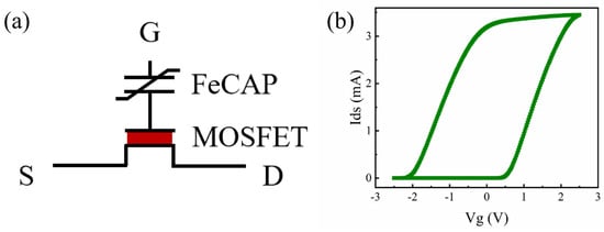
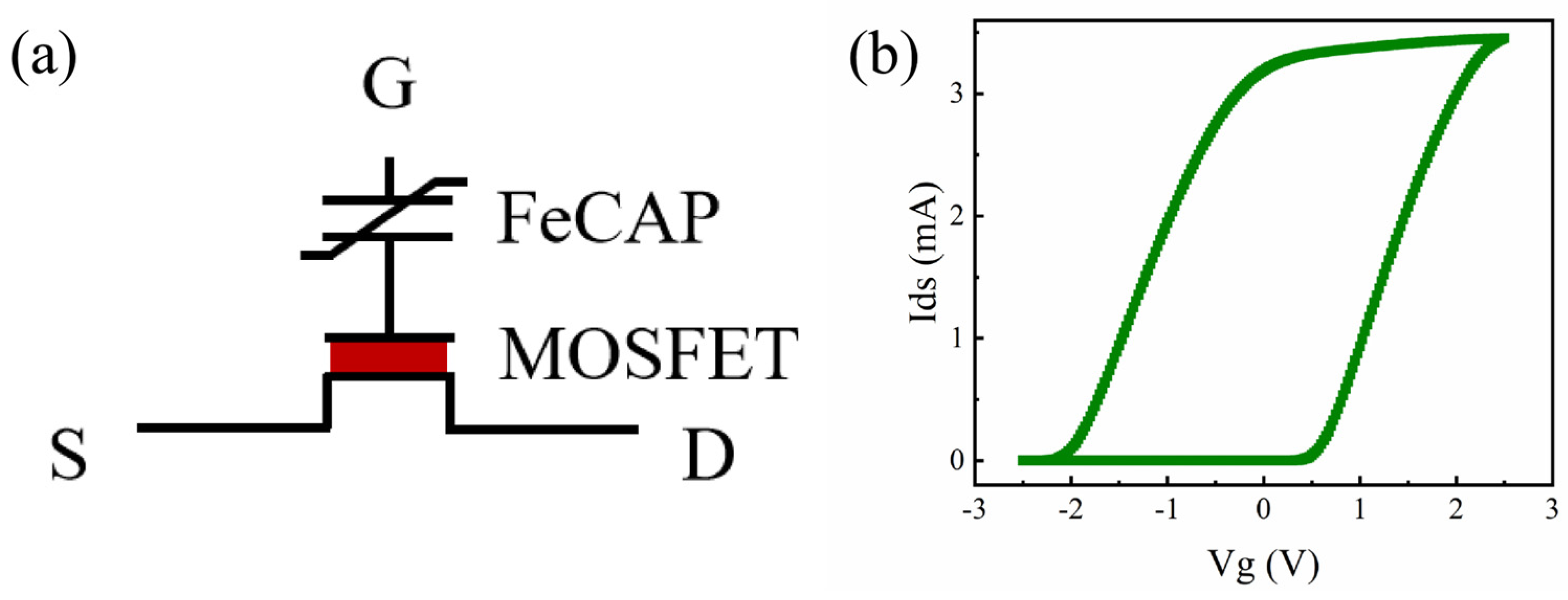
The structure of the FeFET model is shown in Figure 1a. It consists of a ferroelectric capacitor connected in series with a MOSFET gate stage [14,15,16]. In this paper, the Lim model was adopted to model ferroelectric capacitors [17,18]. The transfer characteristic curve simulation of FeFET was carried out, and the result is shown in Figure 1b. Unlike conventional MOSFETs, the transfer characteristic curve of FeFETs is a loop. Therefore, depending on the polarization direction, FeFETs have two different threshold voltages. When FeFET is in a low-threshold voltage state, applying a small voltage can conduct. However, When the FeFET is in a high-threshold voltage state, applying a small voltage to the FeFET will keep it in the off state.
Figure 1.
(a) Structure of the FeFET model. (b) Ids–Vg curve of the FeFET by Spice simulation.
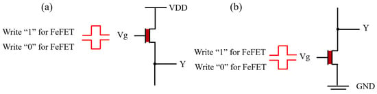
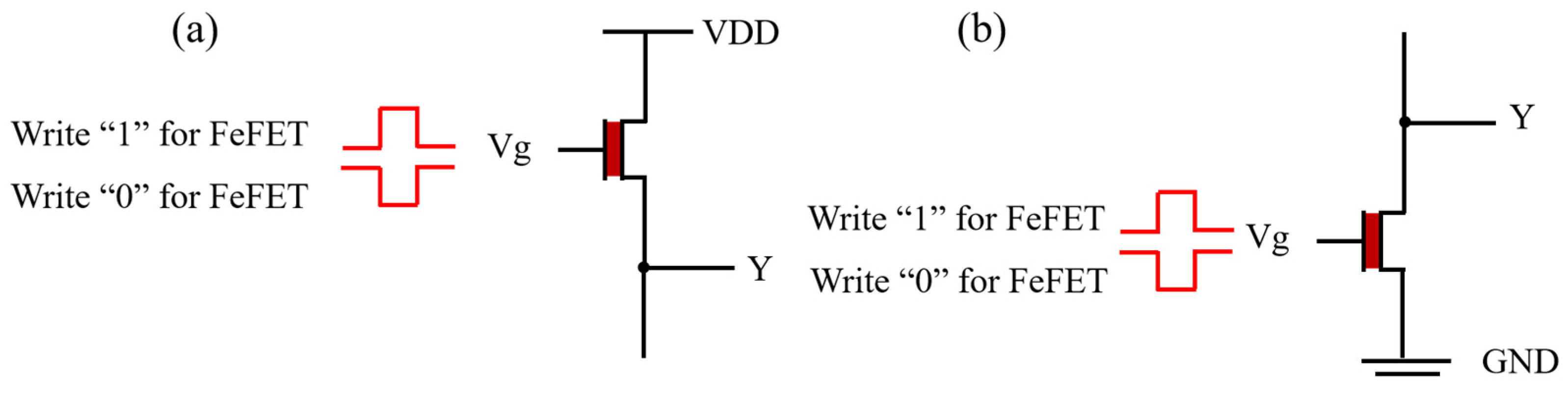
CMOS logic circuits are composed of pull-up networks and pull-down networks. The pull-up network and pull-down network composed of FeFETs are shown in Figure 2. The write voltage is applied on the gate. Input a −2.5 V or +2.5 V voltage pulse at the gate of the FeFET to write “0” or “1”. When the stored data is “0”, the FeFET is in a low-threshold voltage state. A small voltage pulse is applied to the gate of the FeFET, and the output node Y can be raised to VDD or lowered to GND. Through the design of the pull-up network and the pull-down network, a variety of FeFETs-based logic circuits were designed, which can store the weight vectors in the computing circuits. Such FeFETs-CiM ADC-free circuits can reduce a large number of fixed-weight data repetitive reads and support high-precision calculations. This paper presents the FeFETs-CiM CMOS circuits under the 28 nm process, and the simulated VDD is set to 0.9 V.
Figure 2.
(a) Pull-up network based on a single FeFET. (b) Pull-down network based on a single FeFET.
3. ADC-Free CMOS FeFETs-CiM Logic Gate Design
3.1. 2-Bits Logic CMOS Gate Design
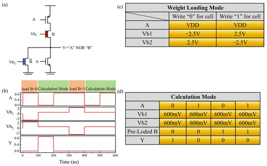
Figure 3a is the structure diagram of the FeFETs-CiM NOR CMOS circuit cell. This NOR gate cell contains two FeFETs: one PMOS and one NMOS. The pull-up network is composed of a PMOS and a FeFET that stores the weight data B connected in series. The pull-down network is composed of an NMOS and a FeFET that stores connected in parallel. The FeFETs-CiM CMOS circuit has two modes: weight loading mode and calculation mode. In the weight loading mode, the weight vector B is written into the two FeFETs through ports Vb1 and Vb2. The port voltage of the FeFETs-CiM NOR gate in the weight loading mode is shown in Figure 3c. The write voltage of the ferroelectric transistor is set to ±2.5 V. Port A maintains VDD to turn off the PMOS. In the calculation mode, the input vector is input through port A, and the ports Vb1 and Vb2 are set with small bias voltages. Under small bias voltage, the data B stored in the ferroelectric transistor will determine its on-off status, thereby completing the NOR operation of A and pre-loaded B. The port voltage of the calculation mode is shown in Figure 3d. If the pre-loaded B = 0, at a bias voltage of 600 mV, the FeFET in the pull-up network is on and the FeFET in the pull-down network is off. Therefore, when the input A is 0, the pull-up network conducts and the pull-down network is off, and the output is VDD; when the input A is 1, the pull-down network conducts, the pull-up network is off, and the output is 0 V. If B = 1, the FeFET in the pull-up network is off and the FeFET in the pull-down network is on. No matter what the value of input A, the pull-up network of FeFETs-CiM NOR gate is turned off, the pull-down network is on, and the output is 0 V. The Spice simulation result of the weight loading mode and the calculation mode are shown in Figure 3b.
Figure 3.
(a) Structure diagram of the FeFETs-CiM NOR CMOS circuit. (b) Spice simulation results of logical calculations of the FeFETs-CiM NOR gate. (c) Port voltage of the FeFETs-CiM NOR gate in the weight loading mode. (d) Port voltage and calculation results of the FeFETs-CiM NOR gate in the calculation mode.
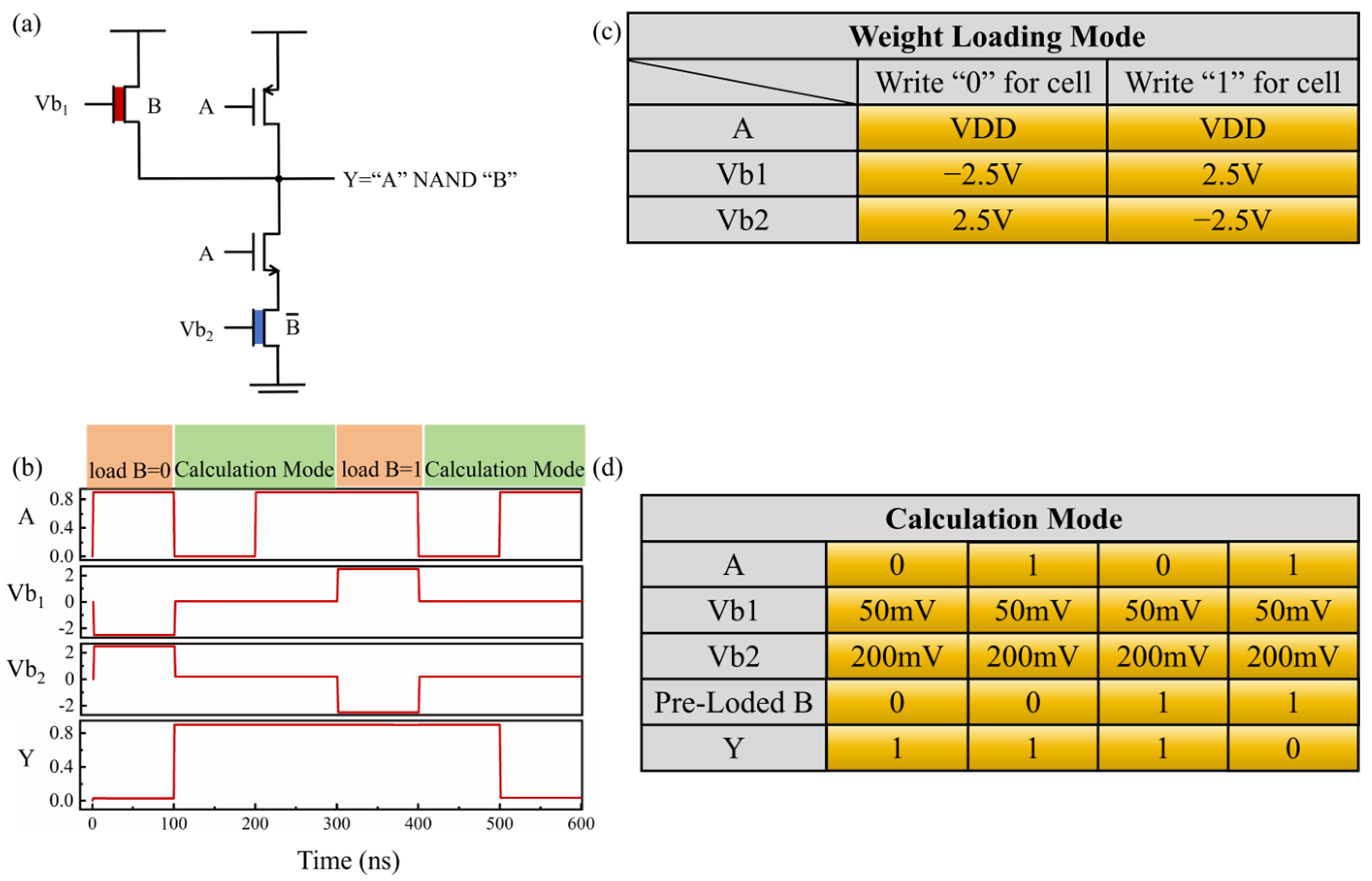
A FeFETs-based NAND CiM gate cell was also designed, the schematic structure of which is shown in Figure 4a. The weight loading mode is the same as that of the FeFETs-CiM NOR gate (Figure 4c). Compared with the FeFETs-CiM NOR gate, the bias voltage of the FeFETs-CiM NAND gate in the calculation mode is set to Vb1 = 50 mV and Vb2 = 200 mV (Figure 4d). When the working bias voltage is 600 mV, it is calculated that when A = 1 and B = 1, the on-resistance (Ron) of the FeFET in the pull-down network is 1.583 kΩ. If it is too large, it will prevent the output from being pulled down to GND. Therefore, we changed the working bias to Vb1 = 50 mV and Vb2 = 200 mV, so that the Ron of the FeFET in the pull-down network was 1.248 kΩ at A = 1 and B = 1, which enhanced the pull-down ability of the FeFETs-CiM NAND gate. If the pre-loaded B = 0, the FeFET in the pull-up network is on and the FeFET in the pull-down network is off. Since the pull-up network of the FeFETs-CiM NAND gate is parallel, no matter what the value of input data A, the pull-up network of the FeFETs-CiM NAND gate is on and the pull-down network is off, the output is VDD. If B = 1, the FeFET in the pull-up network is off and the FeFET in the pull-down network is on. when the input data A = 0, the pull-up network conducts and the pull-down network is off, the output is VDD. when the input data A = 1, the pull-up network is off and the pull-down network is on, the output is 0 V. The verification result of the FeFETs-CiM NAND CMOS circuit’s logical functions is shown in Figure 4b.
Figure 4.
(a) Structure diagram of the FeFETs-CiM NAND CMOS circuit. (b) Spice simulation results of logical calculations of the FeFETs-CiM NAND gate. (c) Port voltage of the FeFETs-CiM NAND gate in the weight loading mode. (d) Port voltage and calculation results of the FeFETs-CiM NAND gate in the calculation mode.
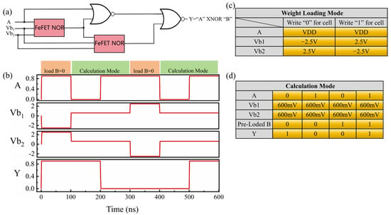
Based on the basic FeFETs-CiM CMOS logic gate circuit that has been designed in this paper, more complex FeFETs-CiM CMOS logic cells can be designed. Figure 5a is a gate-level schematic diagram of the FeFETs-CiM XNOR CMOS circuit. It consists of two FeFETs-CiM NOR gates and two CMOS NOR gates. Note that, it only needs to change the basic logic gate connected to the weight vector input port into FeFETs-CiM logic gate to realize weight storage and logic calculation. The weight vector B can also be stored in the FeFETs and calculated directly when the input signal A arrives through the bias configuration of ports Vb1 and Vb2. The write voltage and the calculated bias voltage is the same as that of the FeFETs-CiM NOR gate (Figure 5c,d). The Spice simulation results of the FeFETs-CiM XNOR gate are shown in Figure 5b. Spice simulation demonstrates that the designed FeFETs-CiM XNOR gate is functionally correct.
Figure 5.
(a) Gate-level structure diagram of the FeFETs-CiM XNOR CMOS circuit. (b) Spice simulation results of logical calculations of the FeFETs-CiM XNOR gate. (c) Port voltage of the FeFETs-CiM XNOR gate in the weight loading mode. (d) Port voltage and calculation results of the FeFETs-CiM XNOR gate in the calculation mode.
3.2. Multi-Bits Logic CMOS Gate Design
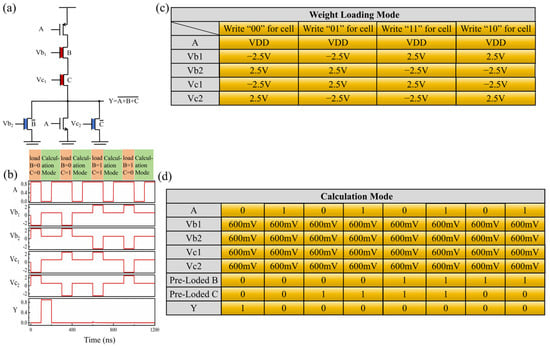
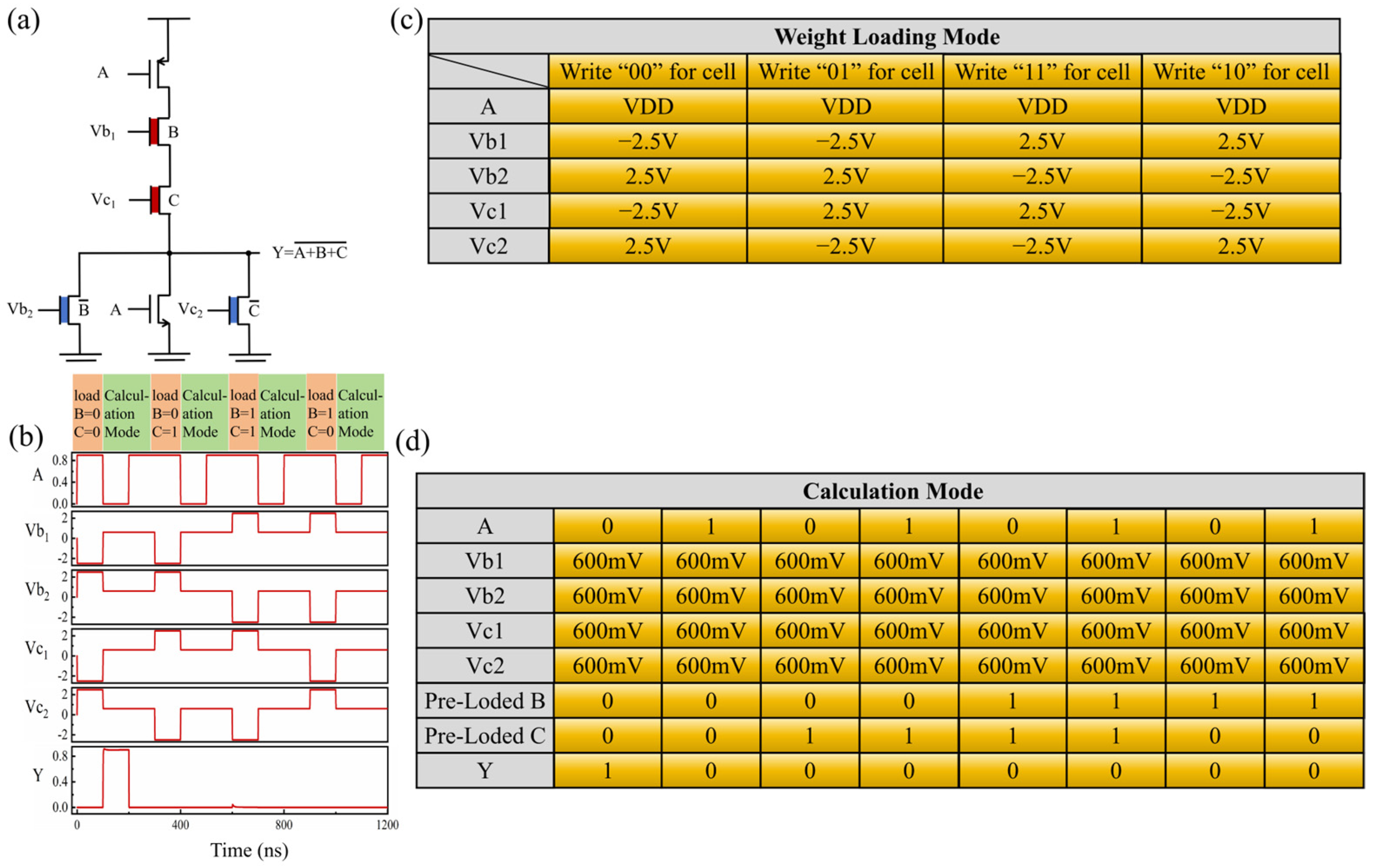
Multi-bit operations are often encountered in combinational logic circuits. Therefore, in addition to designing a variety of 2-bit FeFETs-CiM CMOS logic circuits, multi-bit FeFETs-CiM CMOS logic cells were also designed and optimized in this paper. This enables the FeFETs-CiM circuit we proposed to be more flexibly applicable to various arithmetic logic operations. Figure 6a is a schematic of a 3-bit FeFETs-CiM NOR gate. The pull-up network is composed of one PMOS and two FeFETs connected in series, and the two FeFETs store vectors B and C. The pull-down network of the circuit is composed of one NMOS and two FeFETs connected in parallel. The two FeFETs store vectors and . The weight loading operation is the same as that of the 2-bit FeFETs-CiM NOR gate (Figure 6c). The bias voltage of the four ports Vc1, Vc2, Vb1 and Vb2 in the calculation mode is 600 mV, which is the same as that of the 2-bit FeFETs-NOR gate (Figure 6d). Since the pull-up network of the 3-bit FeFETs-NOR gate is composed of two FeFETs and one PMOS in series, and the three transistors of the pull-down network are in parallel, the pull-up network is on and the pull-down network is off only when the pre-loaded B and C are both 0 the input A is also 0, and the output voltage in this case is VDD. In all other cases, the parallel pull-down network is on, the series pull-up network is off, and the output voltage is 0 V, which is shown in Figure 6b. Two of the three inputs can be stored in FeFETs in the 3-bit FeFETs-CiM logic gate, further reducing data transmission, and they can be flexibly designed and configured according to algorithmic computing requirements. The FeFETs-CiM circuits can achieve multi-bits computing without involving multi-bits storage, reducing the reliance on the storage margin of FeFETs and helping to enhance the robustness of the circuit.
Figure 6.
(a) Structure diagram of the 3-bit FeFETs-CiM NOR CMOS circuit. (b) Spice simulation results of the logical calculations of the 3-bit FeFETs-CiM NOR gate. (c) Port voltage of the 3-bit FeFETs-CiM NOR gate in the weight loading mode. (d) Port voltage and calculation results of the 3-bit FeFETs-CiM NOR gate in the calculation mode.
3.3. Latency and Consumption Validation of FeFETs-CiM Logic Gates
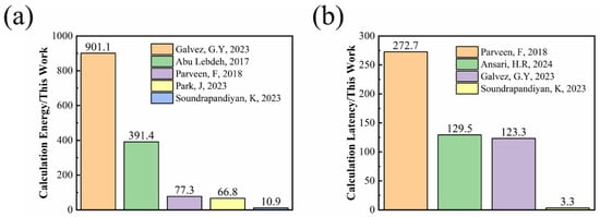
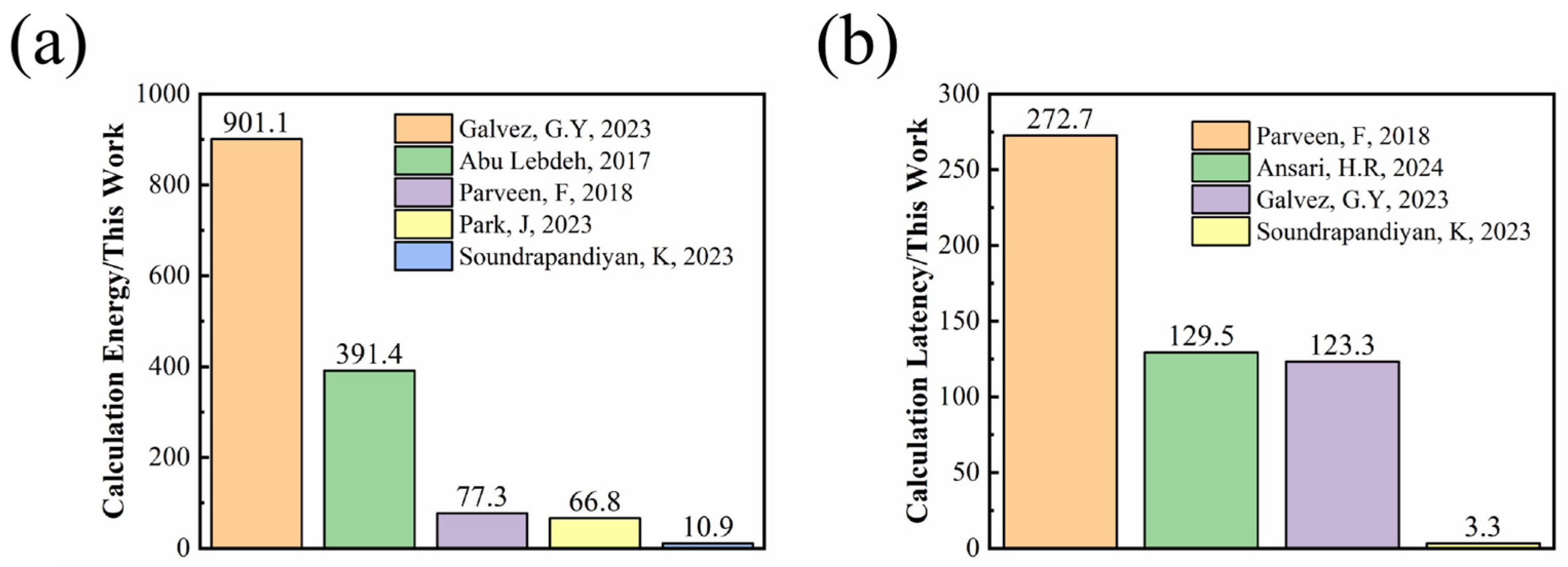
Calculation latency and energy consumption are two of the most important parameters for edge computing devices. Analog CiM circuits contain a large number of ADCs and DACs, which will generate high power consumption and latency. FeFETs-CiM circuits achieve high energy efficiency and low latency. This is achieved by eliminating ADC/DAC overhead, avoiding polarization flips of ferroelectric domains during logic operations, and leveraging the shorter data path of FeFET-based architectures. Table 1 presents the calculation energy consumption and calculation latency of three types of FeFETs-CiM logic gates. The FeFETs-CiM NOR gate has the lowest calculation energy consumption of only 0.0169 fJ/bit. The FeFETs-CiM XNOR gate consists of two FeFETs-CiM NOR gates and two 28 nm CMOS NOR gates, so it has the maximum calculation energy consumption of 0.304 fJ/bit. The energy consumption of the 3-bit FeFETs-CiM NOR gate has increased by 1.86 times, and the latency has increased by 5.14 times. It indicates that the series connection in the pull-up network could increase resistance and degrade energy consumption and latency. However, this is a necessary sacrifice to increase the bit width of the calculation. We compare the calculation energy consumption of FeFETs-CiM XNOR gate with other CiM bitwise operations (Figure 7a) [19,20,21,22,23]. Compared with other CiM circuits, the FeFETs-CiM ADC-free logic gates proposed in this paper can achieve a maximum reduction of 901.1 times in calculation energy consumption. Even compared with the SRAM-CiM circuit with low read and write power consumption, the as-proposed FeFETs-CiM CMOS logic gate circuits have 10.9 times lower calculation energy consumption. We also extracted the calculation latency of the three FeFETs-CiM logic gates at the picosecond level, which is in the same order of magnitude as the 28 nm CMOS logic gate. This paper compares the calculation latency of the FeFETs-CiM XNOR gate with other CiM bitwise operations; the maximum reduction of computation delay is 272.7 times (Figure 7b) [24]. The FeFETs-CiM gate-level circuits have low calculation power consumption and calculation latency while also possessing the high robustness of ADC-free circuits.
Table 1.
Parameters of energy consumption and latency of single FeFETs-CiM CMOS logic gates. (28 nm process, VDD = 0.9 V).
Figure 7.
(a) Calculation energy consumption of the FeFETs-CiM XNOR gate compared with other CiM bitwise operations [19,20,21,22,23]. (b) Calculation latency of the FeFETs-CiM XNOR gate compared with other CiM bitwise operations [19,21,23,24].
4. FeFETs-CiM kNN Distance Calculator Design
FeFETs-CiM circuits are ADC-free and built upon a standard CMOS circuit, which can flexibly design application-specific AI accelerator according to algorithm requirements. In this section, we design an application specific FeFETs-CiM 8-bit calculator and evaluate the performance improvements owing to the proposed FeFETs-CiM CMOS circuits at the system level taking the k-nearest neighbor (kNN) algorithm as an example. The design of an application specific FeFETs-CiM 8-bit calculator can demonstrate that our FeFETs-CiM basic logic gates can be composed to perform more complex tasks.
A kNN, unlike deep neural networks, does not require substantial training of parameters, allowing easy adoption in several edge computing applications [25]. kNN algorithms mainly depend on calculating distance metrics like Euclidean distance, Manhattan distance and Minkowski distance between data elements. However, computing such kNN distance for large datasets require massive amounts of data movements and arithmetic operations. A typical kNN algorithm includes two main computation steps: a kNN distance calculation and top-k sorting. It should be noted that the main bottleneck restricting the kNN algorithm is the calculation of the kNN distance. We adopt the Manhattan distance as the kNN distance metric in our kNN evaluation because it depends on arithmetic addition/subtraction.
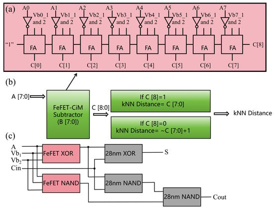
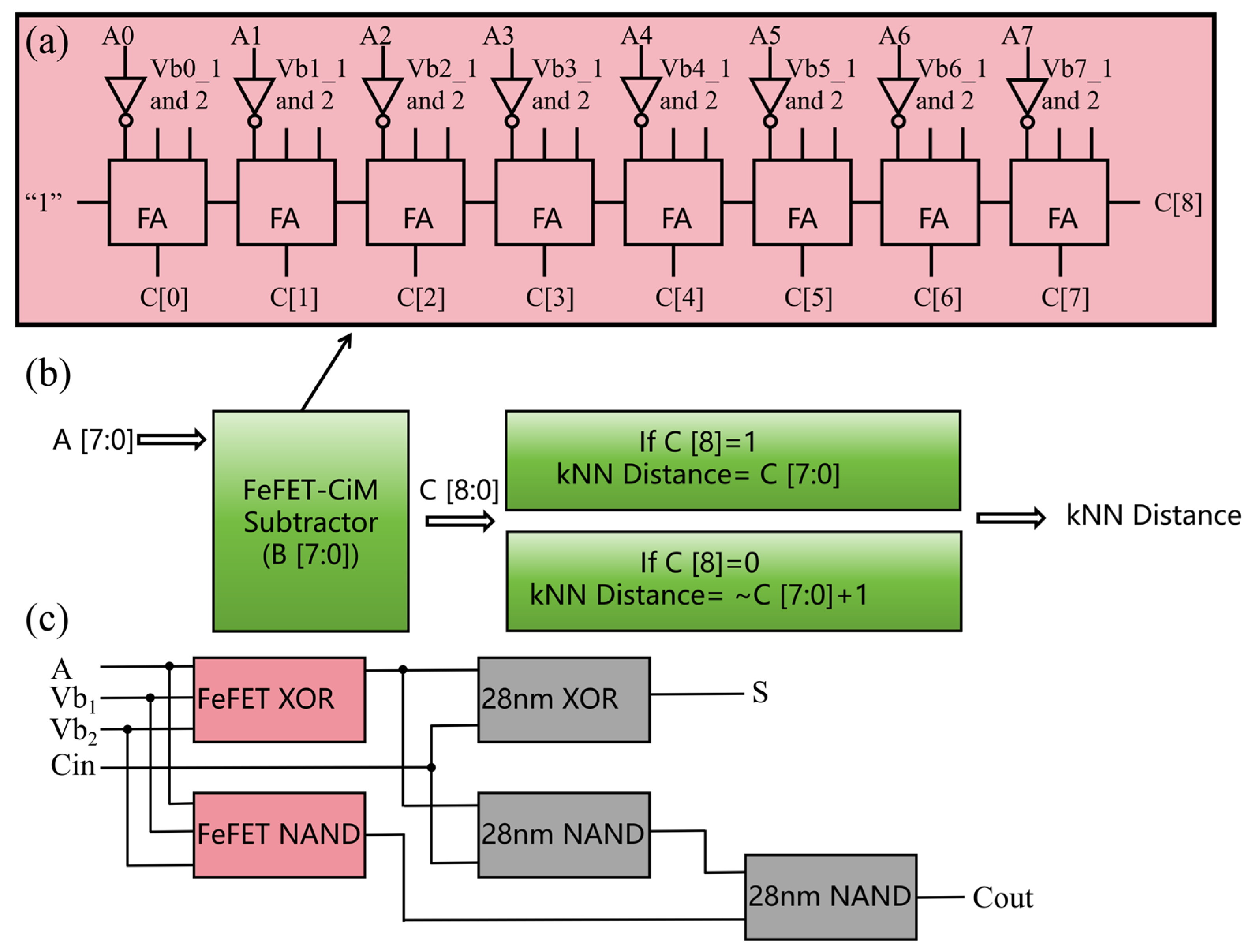
A kNN was evaluated using the recognition of MNIST datasets. Each image in the MNIST datasets of test data and train data is quantized to the INT8 data type and subsequently decomposed into 784 individual 8-bit vectors. The kNN distance is calculated by subtracting the corresponding 8-bit vector and taking its absolute value. For this purpose, we have designed an application specific FeFETs-CiM kNN 8-bit subtractor, which includes eight FeFETs-CiM full adders and eight inverters (Figure 8a). Test data A [7:0] is input into the FeFETs-CiM full adders through the inverter. Meanwhile, the carry input signal of the least significant bit full adder is set to 1 to take the complement code for test data A [7:0]. Train data B [7:0] is fixed weight data. In the weight loading mode, it is written into the FeFETs-CiM kNN 8-bit subtractor through Vbx_1 and Vbx_2. In the calculation mode, it is subtracted from test data to obtain C [8:0], where C [8] is the sign bit; if C [8] = 1, kNN distance is C [7:0]; if C [8] = 0, kNN distance is C [7:0] bitwise inverted and plus 1. The 8-bit kNN distance calculator based on the application specific FeFETs-CiM kNN 8-bit subtractor is shown in Figure 8b. The FeFETs-CiM full adder is composed of a FeFETs-CIM XOR gate, FeFETs-CiM NAND gate, CMOS XOR gate and CMOS NAND gate. Its structural diagram is shown in Figure 8c.
Figure 8.
(a) Structure diagram of the application specific FeFETs-CiM kNN 8-bit subtractor. (b) 8-bit kNN distance calculator based on application specific FeFETs-CiM kNN 8-bit subtractor. (c) Structure diagram of the FeFETs-CiM full adder circuit.
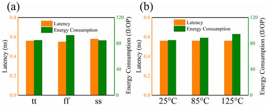
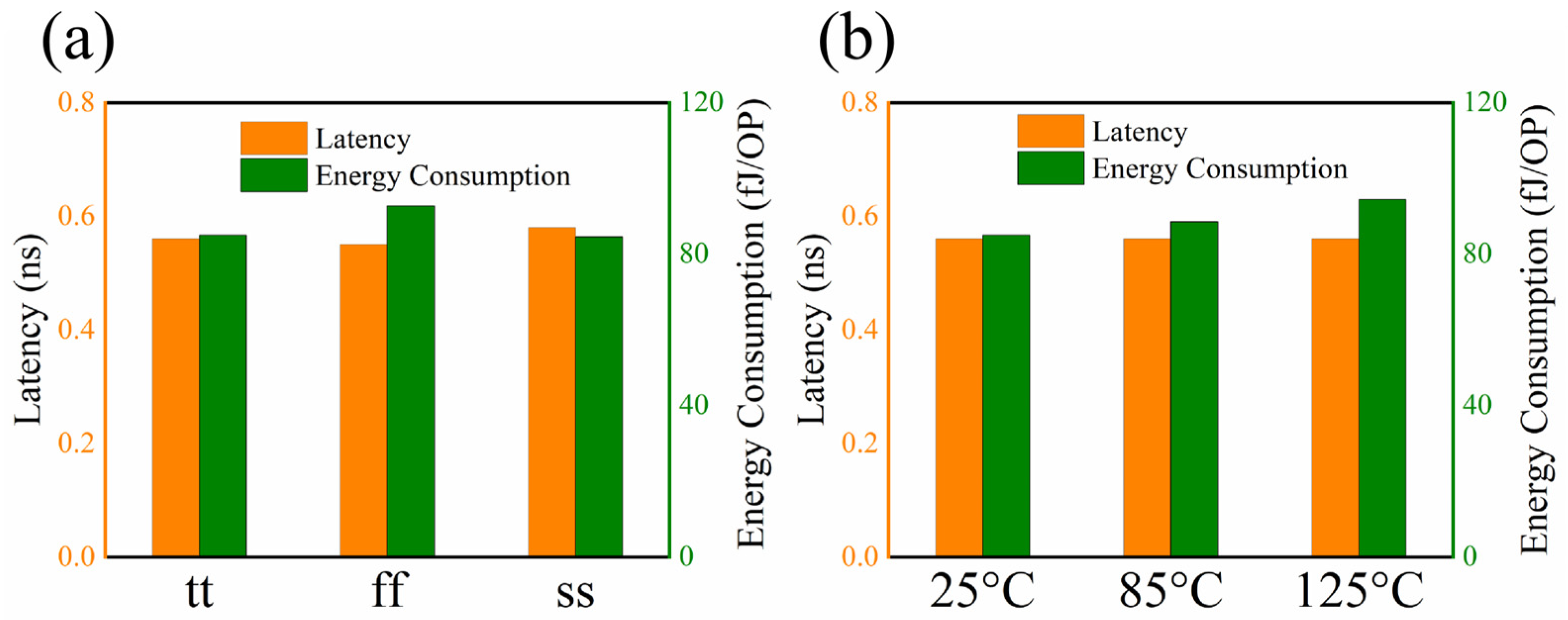
The calculation latency of the FeFETs-CiM 8-bit kNN distance calculator is 0.56 ns and the energy consumption is 85.02 fJ/OP under the operating frequency of 500 MHz (1 OP = 8 bit |a − b|). Figure 9 shows that the worst energy consumption at different process corners and operating temperatures is only 94.5 fJ/OP (TT_125 °C), and the worst latency is only 0.58 ns (SS_25 °C). This illustrates the promising application prospect of high robustness FeFETs-CiM circuits in low power and high speed ASIC. All the latency and energy consumption were extracted by Spice simulation, Synopsys Design Compiler and PrimeTime PX (PTPX) under VDD = 0.9 V.
Figure 9.
(a) Latency and energy consumption of the FeFETs-CiM 8-bit kNN distance calculator under different process corners (b) Latency and energy consumption of the FeFETs-CiM 8-bit kNN distance calculator at different temperatures under a TT process corner (technology = 28 nm, operating frequency = 500 MHz, VDD = 0.9 V, 1 OP represents an 8-bit kNN distance calculation).
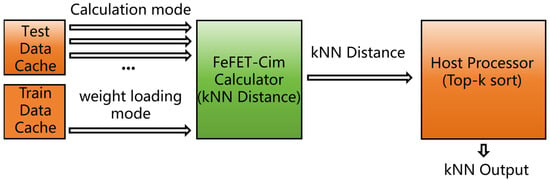
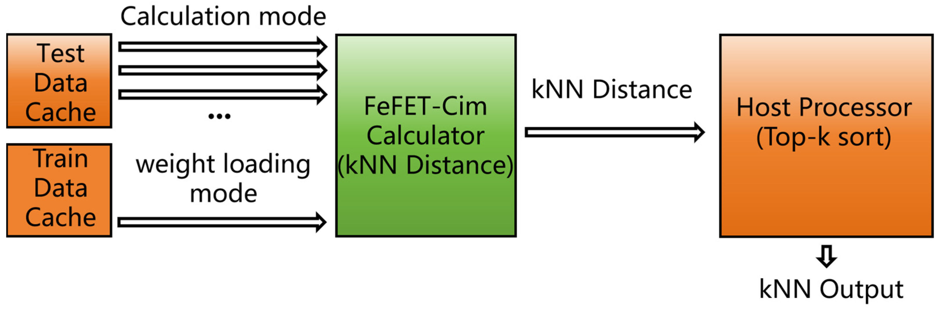
Figure 10 shows the CiM architecture based on the proposed FeFETs-CiM 8-bit subtractor for accelerating kNN. In the weight loading mode, the train data is loaded from the cache into the FeFETs-CiM calculator. After that, the system does not enter weight loading mode unless the train data is updated. In the calculation mode, the test data is input from the cache to the FeFETs-CiM calculator for kNN distance calculation while the sorting computations are performed in the host processor. Note, that under the von Neumann architecture, the calculation of kNN distance and sorting computations are both performed in the host processor, which generates a large amount of data access and data movement. On the contrary, the FeFETs-CiM architecture decreases the amount of data access and data movements substantially due to the in-situ computations. Table 2 shows the amount of data access when the FeFETs-CiM architecture and the von Neumann architecture execute the kNN algorithm under the condition that the test data is 300 MNIST handwritten graphs and the train data is 1000 MNIST handwritten graphs. Since the FeFETs-CiM architecture only accesses the train data in the weight loading mode and does not access the train data in the calculation mode, the FeFETs-CiM architecture reduces train data access by 300 times and total data access by 231 times compared to the von Neumann architecture. The FeFETs-CiM architecture achieves a recognition accuracy of 94% in executing kNN image recognition tasks.
Figure 10.
CiM architecture based on the proposed FeFETs-CiM 8-bit subtractor for accelerating kNN.
Table 2.
Amount of data access when the FeFETs-CiM architecture and the von Neumann architecture execute the kNN algorithm.
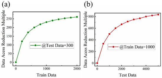
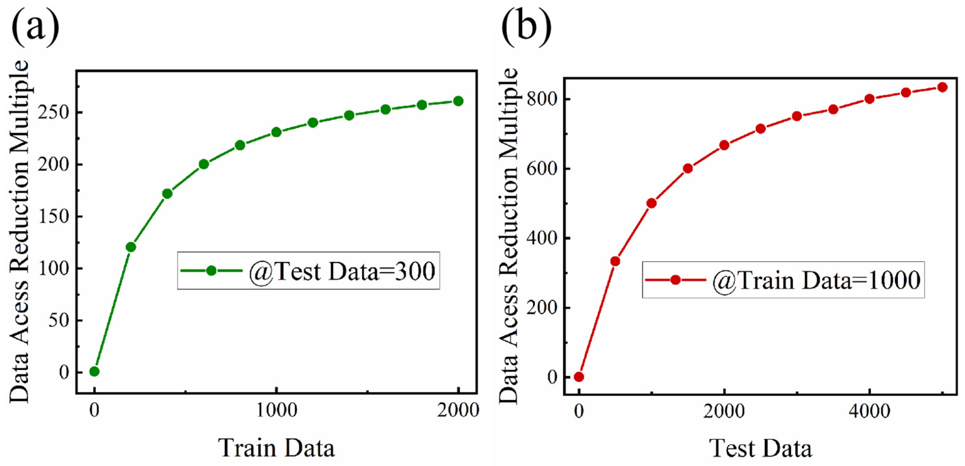
The amount of train data is an important factor affecting the calculation accuracy of kNN algorithm, but increasing the amount of train data will lead to an increase in data transmission power and calculation power. Figure 11a shows the relationship between the data access reduction of the FeFETs-CiM accelerator compared to von Neumann architecture associated with the amount of train data. When the amount of train data increases, the ability of the FeFETs-CiM architecture to reduce data access also increases. This can significantly reduce the transmission power consumption and effectively slow down the increase in power consumption as the amount of train data increases. Figure 11b indicates that as the amount of test data increases, the ability of the FeFETs-CiM architecture to reduce transmission power consumption also increases accordingly. It can be obtained that when the kNN algorithm is executed, the calculation formula of the “Data Access Reduction Multiple” of the FeFETs-CiM architecture compared to the von Neumann architecture is:
where R is “Data Access Reduction Multiple” compared to the von Neumann architecture, I is the amount of input test data, and W is the amount of train data. Specifically, executing the kNN algorithm under the von Neumann architecture necessitates I accesses to the test data and I × W accesses to the train data, resulting in the numerator I + I × W of Equation (1). Conversely, the FeFETs-CiM architecture requires I test data accesses and W train data accesses, yielding the denominator I + W. In an ideal condition, the number of train data W is relatively fixed, and the amount of input data I is constantly increasing. When I tends to infinity, dividing both the numerator and denominator by I in Formula (1) can be simplified as follows:
R = I (W + 1)/(I + W)
R = W + 1
Figure 11.
(a) The relationship between the data access reduction multiple of the FeFETs-CiM accelerator compared to von Neumann architecture associated with the amount of train data (Amount of test data = 300). (b) The relationship between the data access reduction multiple of the FeFETs-CiM accelerator compared to von Neumann architecture associated with the amount of test data (Amount of train data = 1000).
Equation (2) shows that when the amount of train data increases due to the increasing demand for calculation accuracy, the ability of the FeFETs-CiM architecture to reduce transmission power consumption also increases.
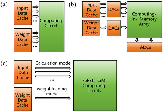
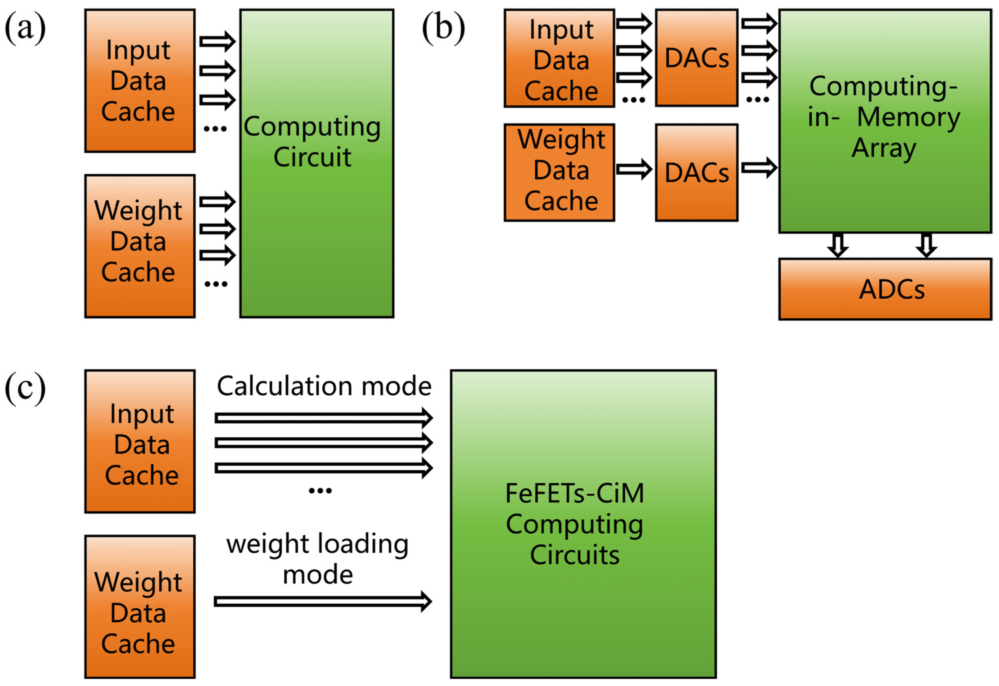
Finally, the performance between the computing-in-memory system of a memristors array [26,27], the von Neumann architecture, and the FeFETs-CiM architecture proposed in this paper is discussed. The neural network architecture using an FeFETs-CiM computing circuit has the advantages of high precision and low transmission power consumption and latency. The traditional digital AI accelerator based on von Neumann architecture needs to read the input data and weight data from the cache into the calculation circuit for each calculation (Figure 12a). Although it has great calculation accuracy, the same weight data needs to be read repeatedly into the calculation circuit each time, resulting in a large amount of transmission power consumption. The computing-in-memory system of memristor array represented by RRAM needs to convert the input signal into analog voltage/current, then input it into the memristor array for calculation, and finally convert the calculated analog value into digital value for output (Figure 12b). Such a computing architecture has low computing accuracy in multi-bit computations, and a large number of ADCs and DACs will increase power consumption of system. The FeFETs-CiM ADC-free computing circuit system loads the weight data only one time into the FeFETs-CiM computing circuit during the weight loading mode, and reads the input data from the cache into the FeFETs-CiM computing circuit for calculation during the calculation mode (Figure 12c). Although the current endurance of FeFETs is not high (around 108), the FeFETs-CiM circuit has the characteristics of a small amount of loading and multiple calculations. The endurance of 108 fully meets the application requirements [28]. In this way, in addition to reloading the weight data when the model is trained for weight data update, the rest of the time only needs to read the input data into the FeFETs-CiM computing circuit and calculate with the pre-loaded weight data. The FeFETs-CiM computing circuit system has the same calculation accuracy as the traditional digital AI accelerator, without the large number of ADCs and DACs in the memristor computing-in-memory system. Meanwhile, the FeFETs-CiM computing circuit system reduces the transmission power consumption of a large amount of weight data.
Figure 12.
(a) Structure diagram of the von Neumann architecture. (b) Structure diagram of the computing-in-memory system of a memristors array. (c) Structure diagram of the FeFETs-CiM ADC-free computing circuit system.
5. Conclusions
This paper has proposed and validated a novel ADC-free CiM architecture utilizing FeFETs to overcome von Neumann bottlenecks and analog CiM limitations. CMOS FeFETs-CiM logic gates (NOR/NAND/XNOR) embedding non-volatile weight storage via FeFETs’ polarization-dependent threshold voltage modulation were designed, eliminating repetitive weight transfers and reducing data movement energy. The FeFETs-CiM CMOS circuits eliminate ADCs/DACs modules through digital operation, resolving analog CiM’s precision degradation in multi-bit computations while saving power overhead by 901.1 times and reducing calculation latency by 272.2 times. Through the design of the pull-up network and the pull-down network, multi-bit FeFETs-CiM logic gates can be flexibly designed according to the algorithm requirements, and multiple input vectors can be configured in FeFETs. Finally, an application specific FeFETs-CiM 8-bit subtractor for kNN distance calculation was designed, where energy consumption is as low as 85.02 fJ/OP and latency is as low as 0.56 ns under 500 MHz operation frequency. The calculation robustness of the FeFETs-CiM kNN distance calculator was ensured by simulating under different process corners and temperatures. The performance improvements owing to the proposed FeFETs-CiM CMOS circuits at the system level were evaluated by taking the kNN algorithm as an example, which can ensure the reduced data access by more than 300 times. Moreover, as the demand for train data increases and the amount of input data increases, the FeFETs-CiM architecture can reduce more data transmission energy, which is of great significance for the further development of low-power edge computing devices.
Author Contributions
Conceptualization, C.H., W.L. and J.L.; methodology, C.H. and T.D.; software, C.H., Q.L. and Z.X.; validation, C.H., J.L. and Z.X.; investigation, C.H. and J.L.; resources, W.L. and J.L.; writing—original draft preparation, C.H.; writing—review and editing, C.H. and J.L.; visualization, C.H.; supervision, W.L. and J.L.; project administration, W.L., J.L. and C.H.; and funding acquisition, W.L., J.L. and T.D. All authors have read and agreed to the published version of the manuscript.
Funding
This research was funded by Pre-Research Program of China, grant number 31512050302. This research was funded by Technologies R & D Program of China, grant number 2006ZYGJ0206.
Data Availability Statement
Data are contained within the article.
Acknowledgments
We thank our colleagues from the State Key Laboratory of Electronic Thin Films and Integrated Devices, School of Integrated Circuit Science and Engineering, and University of Electronic Science and Technology of China, who provided insight and expertise that greatly assisted the research and improved the manuscript.
Conflicts of Interest
The authors declare no conflicts of interest.
References
- Kudo, K.; Aiba, Y.; Hasegawa, K.; Li, X.; Sano, Y.; Sanuki, T. Energy-Efficient In-Memory Computing using 3D Flash Memory with Sequential Multi-Block Activation and Current Control Cell (CC cell). In Proceedings of the 2025 IEEE International Memory Workshop (IMW), Monterey, CA, USA, 18–21 May 2025; IEEE: Piscataway Township, NJ, USA, 2025; pp. 1–4. [Google Scholar] [CrossRef] [Scilit]
- Hsu, H.-H.; Wen, T.-H.; Wu, P.-C.; Jhang, C.-J.; You, D.-Q.; Chen, P.-C.; Chang, M.-F. Challenges in Circuits of Nonvolatile Compute-In-Memory for Edge AI Chips. In Proceedings of the 2023 IEEE 66th International Midwest Symposium on Circuits and Systems (MWSCAS), Tempe, AZ, USA, 6–9 August 2023; IEEE: Piscataway Township, NJ, USA, 2023; pp. 98–102. [Google Scholar] [CrossRef] [Scilit]
- Roshna, M.R.; Suresh, K.E. Design of Energy Efficient SRAM Based In Memory Computing. In Proceedings of the 2025 3rd International Conference on Integrated Circuits and Communication Systems (ICICACS), Raichur, India, 21–22 February 2025; IEEE: Piscataway Township, NJ, USA, 2025; pp. 1–8. [Google Scholar] [CrossRef] [Scilit]
- Jiang, L.; Sun, S.; Ge, J.; Zhang, H.; Kang, W. An In-Memory-Computing STT-MRAM Macro with Analog ReLU and Pooling Layers for Ultra-High Efficient Neural Network. In Proceedings of the 2023 IEEE 12th Non-Volatile Memory Systems and Applications Symposium (NVMSA), Niigata, Japan, 30 August–1 September 2023; IEEE: Piscataway Township, NJ, USA, 2023; pp. 44–49. [Google Scholar] [CrossRef] [Scilit]
- AParmar, A.; Prasad, K.; Rao, N.; Mekie, J. An Automated Approach to Compare Bit Serial and Bit Parallel In-Memory Computing for DNNs. In Proceedings of the 2022 IEEE International Symposium on Circuits and Systems (ISCAS), Austin, TX, USA, 27 May–1 June 2022; IEEE: Piscataway Township, NJ, USA, 2022; pp. 2948–2952. [Google Scholar] [CrossRef] [Scilit]
- Lee, J.; Park, B.-G.; Kim, Y. Implementation of Boolean Logic Functions in Charge Trap Flash for In-Memory Computing. IEEE Electron Device Lett. 2019, 40, 1358–1361. [Google Scholar] [CrossRef] [Scilit]
- Kim, S.; Yoo, H.-J. An Overview of Computing-in-Memory Circuits with DRAM and NVM. IEEE Trans. Circuits Syst. II Express Briefs 2024, 71, 1626–1631. [Google Scholar] [CrossRef] [Scilit]
- Lin, Z.; Zhan, H.; Li, X.; Peng, C.; Lu, W.; Wu, X.; Chen, J. In-Memory Computing with Double Word Lines and Three Read Ports for Four Operands. IEEE Trans. Very Large Scale Integr. (VLSI) Syst. 2020, 28, 1316–1320. [Google Scholar] [CrossRef] [Scilit]
- Shi, Y.; Oh, S.; Huang, Z.; Lu, X.; Kang, S.H.; Kuzum, D. Performance Prospects of Deeply Scaled Spin-Transfer Torque Magnetic Random-Access Memory for In-Memory Computing. IEEE Electron Device Lett. 2020, 41, 1126–1129. [Google Scholar] [CrossRef] [Scilit]
- Wang, Z.-R.; Li, Y.; Su, Y.-T.; Zhou, Y.-X.; Cheng, L.; Chang, T.-C.; Xue, K.-H.; Sze, S.M.; Miao, X.-S. Efficient Implementation of Boolean and Full-Adder Functions with 1T1R RRAMs for Beyond Von Neumann In-Memory Computing. IEEE Trans. Electron Devices 2018, 65, 4659–4666. [Google Scholar] [CrossRef] [Scilit]
- Wang, S.; Ma, Y.; Kang, Y. AFT-CIM: An Energy Efficient ADC-Free Transpose Computing-in-Memory Macro for MAC Operations. In Proceedings of the 2024 IEEE International Symposium on Circuits and Systems (ISCAS), Singapore, 19–22 May 2024; IEEE: Piscataway Township, NJ, USA, 2024; pp. 1–5. [Google Scholar] [CrossRef] [Scilit]
- Wang, S.; Ma, Y.; Kang, Y. A Brain-Inspired ADC-Free SRAM-Based In-Memory Computing Macro with High-Precision MAC for AI Application. IEEE Trans. Circuits Syst. II Express Briefs 2023, 70, 1276–1280. [Google Scholar] [CrossRef] [Scilit]
- Jiang, H.; Huang, S.; Li, W.; Yu, S. ENNA: An Efficient Neural Network Accelerator Design Based on ADC-Free Compute-In-Memory Subarrays. IEEE Trans. Circuits Syst. I Regul. Pap. 2023, 70, 353–363. [Google Scholar] [CrossRef] [Scilit]
- Tung, C.-T.; Pahwa, G.; Salahuddin, S.; Hu, C. A Compact Model of Ferroelectric Field-Effect Transistor. IEEE Electron Device Lett. 2022, 43, 1363–1366. [Google Scholar] [CrossRef] [Scilit]
- Ni, K.; Jerry, M.; Smith, J.A.; Datta, S. A Circuit Compatible Accurate Compact Model for Ferroelectric-FETs. In Proceedings of the 2018 IEEE Symposium on VLSI Technology, Honolulu, HI, USA, 18–22 June 2018; IEEE: Piscataway Township, NJ, USA, 2018; pp. 131–132. [Google Scholar] [CrossRef] [Scilit]
- Aziz, A.; Ghosh, S.; Datta, S.; Gupta, S.K. Physics-Based Circuit-Compatible SPICE Model for Ferroelectric Transistors. IEEE Electron Device Lett. 2016, 37, 805–808. [Google Scholar] [CrossRef] [Scilit]
- Lim, K.; Kim, K.; Hong, S.; Lee, K. A semi-empirical cad model of ferroelectric capacitor for circuit simulation. Integr. Ferroelectr. 1997, 17, 97–104. [Google Scholar] [CrossRef] [Scilit]
- Chen, Z.; Lim, M.; Joshi, V.; De Araujo, C.A.P.; Mcmillan, L.D. Advanced simulation tool for FeRAM design. Integr. Ferroelectr. 2001, 40, 101–112. [Google Scholar] [CrossRef] [Scilit]
- Galvez, G.Y.; Lim, A.J.; Camarillo, C.J.; Marturillas, J.R.; Teodoro, M.E.; Urfano, E.K.N.; Alvarez, A.; Antonio, R.A.; Galapon, F.A.; Baquiran, S.J.A.; et al. Integration of In-Memory Computing Capabilities to a Self-Matching Complementary-Reference Sensing Scheme for TST-MRAM. In Proceedings of the 2023 20th International SoC Design Conference (ISOCC), Jeju, Republic of Korea, 25–28 October 2023; IEEE: Piscataway Township, NJ, USA, 2023; pp. 285–286. [Google Scholar] [CrossRef] [Scilit]
- Abu Lebdeh, M.; Abunahla, H.; Mohammad, B.; Al-Qutayri, M. An Efficient Heterogeneous Memristive xnor for In-Memory Computing. IEEE Trans. Circuits Syst. I Regul. Pap. 2017, 64, 2427–2437. [Google Scholar] [CrossRef] [Scilit]
- Parveen, F.; He, Z.; Angizi, S.; Fan, D. HielM: Highly flexible in-memory computing using STT MRAM. In Proceedings of the 2018 23rd Asia and South Pacific Design Automation Conference (ASP-DAC), Jeju, Republic of Korea, 22–25 January 2018; IEEE: Piscataway Township, NJ, USA, 2018; pp. 361–366. [Google Scholar] [CrossRef] [Scilit]
- Park, J. Self-Writing xnor Magnetic Random Access Memory for Binary Neural Network Acceleration. IEEE Trans. Magn. 2023, 59, 3401910. [Google Scholar] [CrossRef] [Scilit]
- Soundrapandiyan, K.; Vishvakarma, S.K.; Reniwal, B.S. Reniwal, Enabling Energy-Efficient In-Memory Computing with Robust Assist-Based Reconfigurable Sense Amplifier in SRAM Array. IEEE J. Emerg. Sel. Top. Circuits Syst. 2023, 13, 445. [Google Scholar] [CrossRef] [Scilit]
- Ansari, H.R.; El-Atab, N. Efficient Implementation of Boolean Logic Functions Using Double Gate Charge-Trapping Memory for In-Memory Computing. IEEE Trans. Electron Devices 2024, 71, 1879–1885. [Google Scholar] [CrossRef] [Scilit]
- Zhang, M.-L.; Zhou, Z.-H. ML-KNN: A lazy learning approach to multi-label learning. Pattern Recognit. 2007, 40, 2038–2048. [Google Scholar] [CrossRef] [Scilit]
- Antolini, A.; Zavalloni, F.; Lico, A.; Vignali, R.; Iannelli, L.; Zurla, R.; Bertolini, J.; Calvetti, E.; Pasotti, M.; Scarselli, E.F.; et al. Controlled Acceleration of PCM Cells Time Drift Through On-Chip Current-Induced Annealing for AIMC Multilevel MVM Computation. IEEE Trans. Electron Devices 2025, 72, 215–221. [Google Scholar] [CrossRef] [Scilit]
- Carletti, F.; Farronato, M.; Hu, G.Y.C.; Lepri, N.; Tortorelli, I.; Pirovano, A.; Fantini, P.; Ielmini, D. 3-D Crosspoint (3DXP) Memory Arrays with Subthreshold Operation for Low-Energy, High-Accuracy Neural Network Accelerators. IEEE Trans. Electron Devices 2026, 73, 264–270. [Google Scholar] [CrossRef] [Scilit]
- Dutta, S.; Ye, H.; Chakraborty, W.; Luo, Y.-C.; Jose, M.S.; Grisafe, B.; Khanna, A.; Lightcap, I.; Shinde, S.; Yu, S.; et al. Monolithic 3D Integration of High Endurance Multi-Bit Ferroelectric FET for Accelerating Compute-In-Memory. In Proceedings of the 2020 IEEE International Electron Devices Meeting (IEDM), San Francisco, CA, USA, 12–18 December 2020; IEEE: Piscataway Township, NJ, USA, 2020; pp. 36.4.1–36.4.4. [Google Scholar] [CrossRef] [Scilit]

Disclaimer/Publisher’s Note: The statements, opinions and data contained in all publications are solely those of the individual author(s) and contributor(s) and not of MDPI and/or the editor(s). MDPI and/or the editor(s) disclaim responsibility for any injury to people or property resulting from any ideas, methods, instructions or products referred to in the content. |
© 2026 by the authors. Licensee MDPI, Basel, Switzerland. This article is an open access article distributed under the terms and conditions of the Creative Commons Attribution (CC BY) license.