


Abstract
Particle physics experiments rely on complex trigger and data acquisition systems, where large channel counts, low latency, compact implementation, and power efficiency are critical requirements. In this context, mixed-signal interfaces are often needed in front-end electronics for signal digitization, monitoring, calibration, and local data processing. Conventional analog data converters, however, may limit scalability when many channels must be integrated in systems based on field-programmable gate arrays (FPGAs) or digital application-specific integrated circuits (ASICs). This work presents synthesizable digital-to-analog converter (DAC) and analog-to-digital converter (ADC) architectures, implemented using fabric FPGA resources. The DAC is based on a digitally controlled delay line and generates a 400 MHz pulse-width-modulated output that can be filtered to obtain a continuous analog voltage. The ADC follows a single-slope architecture for voltage-to-time conversion, and a tapped delay line for time-to-digital conversion at 400 MSps. Both architectures were implemented and experimentally characterized in an AMD Kintex UltraScale+ FPGA. The DAC achieves a 2.3 V dynamic range, an LSB of approximately 5 mV, and an ENOB of 3.9 bit at 500 kHz, full-scale range. The ADC provides a 1.5 V dynamic range, 9-bit output, non-linearity within 1% over the full range, and 6.2 ENOB at 1 MHz, full-scale range. The combined (ADC + DAC) implementation uses less than 2% of a XCKU5P FPGA fabric resources. Our results demonstrate the suitability of the proposed approach for compact, scalable mixed-signal interfaces in experimental physics instrumentation, paving the way for implementation in application-specific integrated circuits.
1. Introduction
Particle physics experiments rely on increasingly complex detector systems in which large numbers of channels must be read out, monitored, calibrated, and processed in real time. Modern high-energy physics (HEP) detectors are complex systems based on heterogeneous sensors, which require front-end and back-end electronics capable of sustaining high data rates while preserving low latency and deterministic timing [1]. These requirements are particularly stringent in trigger and data-acquisition (DAQ) systems (see for example [2,3,4]) where early decisions must often be taken within tight timing constraints and where the amount of data transferred from the detector must be reduced as close as possible to the source.
Field-programmable gate arrays (FPGAs) are widely used in this context because they provide real-time processing, configurable logic, high-speed input/output interfaces, and deterministic timing. They are commonly employed for detector control, data formatting, timing distribution, online filtering, trigger formation, and implementation of real-time algorithms, including machine learning-based selections. Future upgrades of collider experiments [5] are expected to further increase the number of readout channels and the complexity of local processing, making compact and scalable electronics solutions of utmost importance.
Although most of the processing chain is implemented digitally, several functions at the interface with the detector front-end remain intrinsically mixed-signal. Examples include the generation of programmable bias or threshold voltages, calibration signals, slow-control references, and the digitization of analog quantities for diagnostics or local feedback [6,7,8]. In conventional systems, these functions are typically implemented using dedicated analog components or analog intellectual property (IP) blocks. While such solutions can provide excellent performance, they may limit scalability when many channels are required, increase board or silicon area, limit system integration, and reduce portability across FPGA families or digital application-specific integrated circuit (ASIC) design flows.
A complementary approach is to implement data-conversion functions using digital resources only. Synthesizable digital-to-analog converters (DACs) and analog-to-digital converters (ADCs) can be described at the register-transfer level and mapped onto logic elements, clock-management resources, carry chains, and input/output buffers already available in modern FPGAs. This strategy is particularly attractive for experimental physics instrumentation because it can simplify replication over multiple channels, enable tight integration with digital control and processing logic, and provide a direct path toward future digital ASIC implementations. Moreover, even when the achievable resolution is lower than that of dedicated precision converters, such architectures can be sufficient for monitoring, calibration, control, and fast local-processing tasks where compactness, latency, and integration density are primary constraints.
Two of the first FPGA-based ADC implementations are described in [9,10]. They featured a single-slope ADC, where the input voltage is converted into a time interval by comparing it with a reference exponential waveform generated by the FPGA plus an external RC network. They achieved raw resolutions up to 12 bit at 2 MSps and 7 bit at 62.5 MSps. Implementations in recent FPGAs [11,12,13] demonstrated sampling rates from a few hundred MSps to 1.2 GSps with effective number of bits in the range from 6 to 7 bit. However, these implementations require high logic footprints on the order of tens of thousands of look-up tables (LUTs) and flip-flops (FFs). This is mostly related to linearization and calibration logic as well as the complexities of the time-to-digital converter implementations. FPGA-based DACs [14] have been reported to convert 5-bit digital samples at 20 MSps, but they require output pins of the FPGA, when N is the number of bits in the conversion. This clearly limits the maximum number of bits and the scaling of several DAC channels in the device.
The contribution of this work to the state of the art is twofold. In fact, we present two architectures, an ADC and a DAC, optimized for FPGA-based mixed-signal interfaces in particle physics instrumentation. The proposed ADC adopts a single-slope architecture, while the DAC uses a digitally controlled delay line (DCDL) to generate a fine-grained pulse-width-modulated signal. Both converters are designed for slow-control applications, with sampling rates on the order of hundreds of MSps, analog bandwidths up to 1 MHz, and effective resolutions up to 6 bits for the ADC and 4 bits for the DAC. They require only a minimal RC network external to the FPGA, while achieving a logic footprint up to ten times smaller than those of the works cited above. We describe the implementation of our converters and present experimental results from a test bench built around an AMD Kintex UltraScale+ FPGA.
We note that, depending on the installation location of the electronics, some applications in particle physics may require a certain level of radiation tolerance. The use of static random access memory-based FPGAs in radiation environments, including device characterization and mitigation techniques for single-event effects, is extensively discussed in the literature [15,16,17]. However, radiation qualification is design-, device- and environment-specific (see, for example, [18,19]) and requires dedicated validation beyond the scope of this work.
The rest of this paper is organized as follows. Section 2 describes the converter architectures and the logic footprint of the implementation. Section 3 describes the experimental setup used for characterization of the converters and reports the measured performance. Section 4 compares the performance and footprint of our implementations to relevant solutions published in the literature. Finally, Section 5 summarizes our findings.
2. Converter Architectures and Implementation
2.1. ADC
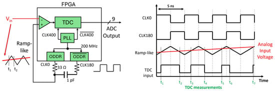
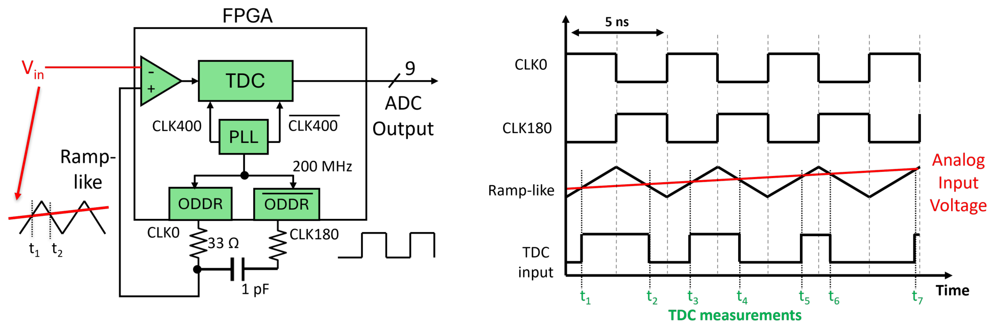
Our solution is inspired by the concepts proposed in [9,10]. In our implementation, the FPGA drives a 200 MHz clock and its inverted replica on two pins operating with LVCMOS18 electrical levels, therefore switching between 0 V and 1.8 V. An external RC network, implemented with two 33 resistors and a 1 pF capacitor, shapes these two digital signals into a periodic ramp-like waveform (see Figure 1).
Figure 1.
Analog-to-digital converter. Left, block diagram of the ADC. Right, timing diagram.
The external circuit feeds the ramp-like signal back into the FPGA through the positive input of a differential input buffer (IBUFDS), while it applies the voltage to be measured, , to the negative input. The buffer therefore acts as a comparator and produces an internal digital signal whose switching instants identify the crossings between the ramp and . We note that the shaping capacitance is dominated by printed circuit board parasitics, of the order of tens of pF. We added the external capacitor for fine tuning of the RC time constant. Moreover, according to the AMD documentation and the settings we used, the FPGA output drivers also introduce a series resistance of about 20 , which further contributes to the shaping. Once the trend of the ramp-like signal as a function of time has been characterized, one can translate the measured crossing instants to analog voltages.
A time-to-digital converter (TDC) measures these crossing times and converts them into digital samples. The TDC samples the comparator output twice per 200 MHz clock cycle, on the rising and falling ramps, achieving a 400 MSps rate. Our converter is based on tapped delay lines (TDLs). For a general description of the operating principles of TDL-based TDCs, see, for example, [20,21]. Our architecture includes two TDLs, each consisting of 54 CARRY8 [22] primitives. A CARRY8 is a chain of eight multiplexers, i.e., the taps, with each multiplexer output sampled by a flip-flop. Thus, the line includes 432 taps. The average delay of a multiplexer has been measured to be 3.5 ps. The 400 MHz system clock (CLK400) samples the first delay line, while its inverted-phase counterpart () samples the second one. Each delay line covers more than ns, i.e., half of the clock period at 400 MHz. The encoder modules convert the thermometer-code data produced by the delay lines into binary words synchronously in their respective clock domains.
The encoder consists of four pipelined bisection stages followed by a final counting stage. Each bisection stage examines a 10-tap window starting at the midpoint of the current delay-line slice and counts the number of taps that sampled the target value. The target value depends on the polarity of the transition being searched: for a 1-to-0 transition, corresponding to a rising-edge crossing, the encoder counts logic ‘1’ samples; for a 0-to-1 transition, corresponding to a falling-edge crossing, it counts logic ‘0’ samples. Based on whether the target value is found in the midpoint window, the encoder selects either the lower or upper half of the slice for the next stage. The slice length is progressively reduced from 432 to 216, 108, 54, and finally 27 taps. In the final stage, the encoder counts the number of samples equal to the target value within the selected 27-tap slice and combines this local count with the weighted bisection index bits to generate the binary output. Each stage adds one clock cycle of latency. Therefore, when operating at 400 MHz, the encoder produces the encoded value after a latency of 12.5 ns. Once the pipeline is filled, a new binary value is output every clock cycle, corresponding to an output period of 2.5 ns.
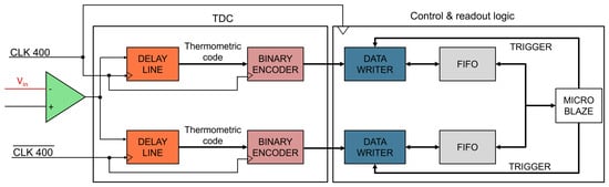
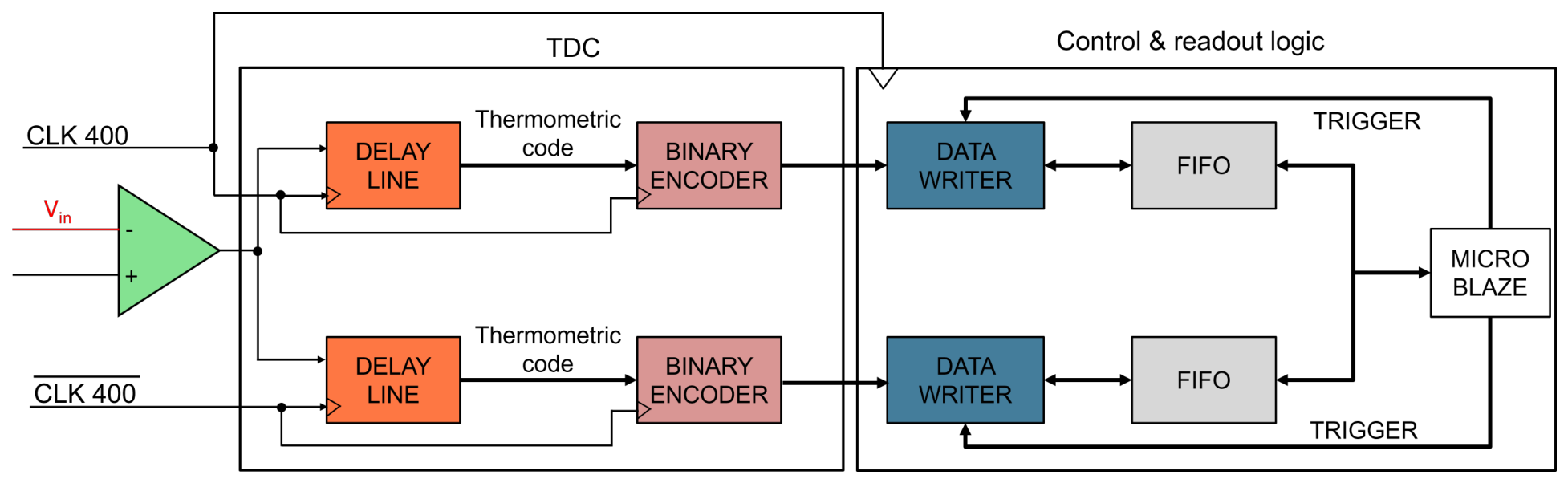
For characterization and control purposes, we designed dedicated ADC test logic controlled by a MicroBlaze soft-core processor, as shown in Figure 2. The logic transfers the data produced in the domain to the CLK400 domain. Since CLK400 and are synchronous clocks with a known phase relationship, we use timing constraints and static analysis to verify this clock-domain transfer, avoiding the need for asynchronous FIFOs. Dedicated data writer modules transfer the encoded samples to two synchronous FIFO buffers, with a depth allowing the acquisition of up to 16,384 consecutive samples.
Figure 2.
Simplified block diagram of the ADC, showing TDC internals and readout logic. A clock domain crossing, to CLK400, occurs between the bottom encoder and data writer.
2.2. DAC
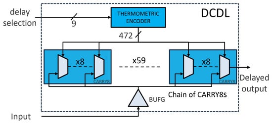
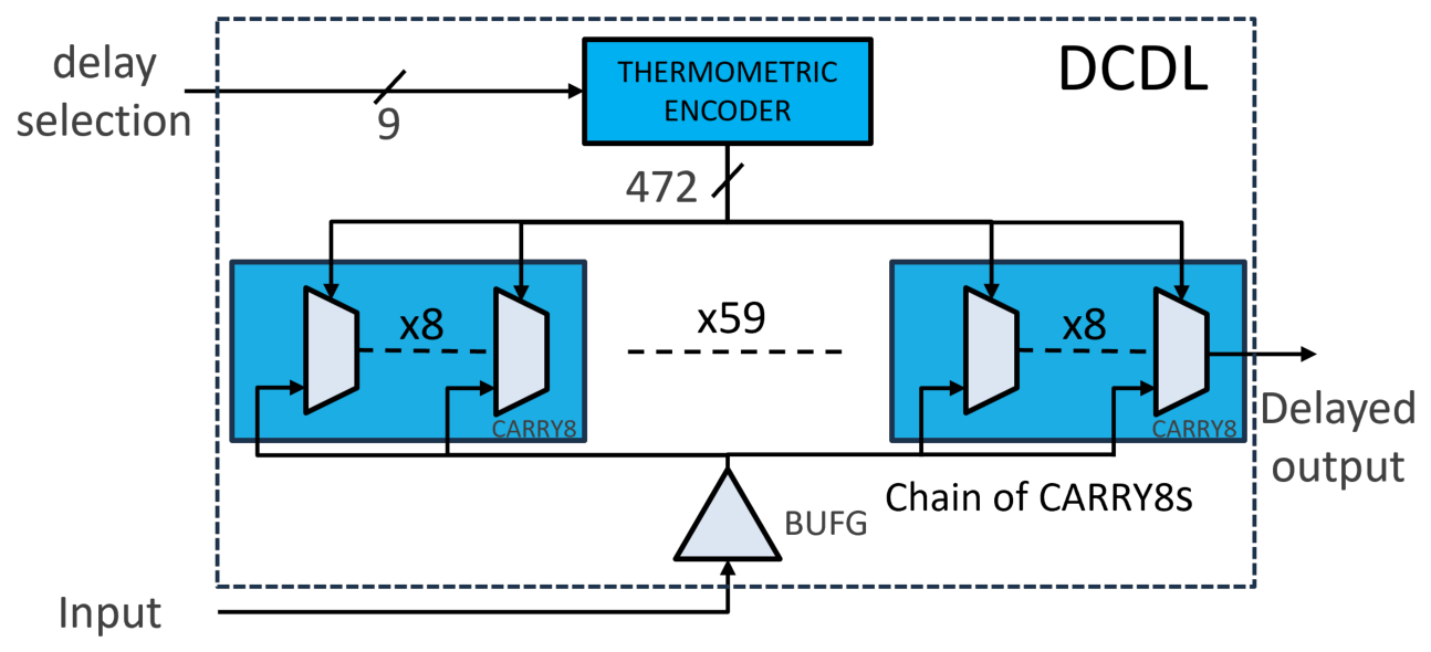
Our architecture is built around the digitally controlled delay line (DCDL) described in [23] and patented in [24]. The DCDL exploits the clock distribution tree to deliver the input signal to a chain of CARRY8 primitives (Figure 3). Each multiplexer in the CARRY8 is a possible entry point in the chain and, if selected for propagation of the signal, contributes to the overall input-to-output delay. Since the delay through the clock distribution tree is approximately uniform, the overall delay can be deterministically controlled by driving the multiplexer selection signals, thereby introducing a programmable delay. This increases or decreases the path length that the signal must travel. In our implementation, the DCDL includes 59 CARRY8 primitives, or 472 multiplexers, for a programmable delay up to nearly 1.65 ns.
Figure 3.
Simplified block diagram of the DCDL.
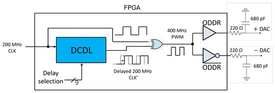
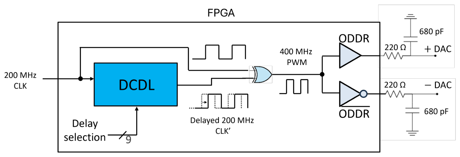
A block diagram of the design is shown in Figure 4. The DAC is driven by a 200 MHz clock and internally generates a delayed replica of this signal through the DCDL. The original and delayed clocks are then sent as inputs to an XOR gate to produce a 400 MHz pulse-width-modulated (PWM) signal. Unlike phase- or delay-locked loop approaches, the DCDL is open-loop. Its delay can be updated at each 200 MHz clock cycle, providing a fast modulation of the duty cycle. The LSB of the pulse-width modulation corresponds to one delay element of the DCDL, i.e., one multiplexer of the CARRY8 primitive.
Figure 4.
Simplified block diagram of the DAC.
The PWM signal is then routed through a clock buffer to two ODDR primitives, which generate an output and its inverted copy on a pair of FPGA pins. This differential configuration was chosen to enable the generation of negative voltages. The differential output is finally filtered by an external RC network to attenuate high-frequency components and recover the analog modulating signal.
The MicroBlaze-based system designed for the ADC also feeds the DAC input via a dedicated FIFO.
2.3. Logic Footprint and Scalability
We implemented one channel of ADC and DAC in an AMD Kintex UltraScale+ XCKU5P FPGA. The ADC and DAC logic occupy less than 2% of the device’s resources (Table 1). The table also accounts for auxiliary MicroBlaze-based logic for test and control functions.
Table 1.
FPGA resource utilization for the ADC, DAC, ADC + DAC total, and test logic.
Assuming independent replication of the converter datapaths, LUT, FF, and carry-chain utilization is expected to increase approximately linearly with the number of channels. For example, neglecting shared resources, 16 ADC+DAC channels would require approximately 47,264 LUTs, 64,000 FFs, and 2816 CARRY8 primitives, corresponding to approximately 22% of LUTs, 15% of FFs, and 12% of CARRY8 resources on the XCKU5P. However, several resources can be shared among multiple channels. In particular, the clock-generation and control logic need not be replicated, and the ramp-generation circuitry of the ADC might be shared by a group of channels, depending on the chosen FPGA I/O banks. Therefore, the overall resource growth is expected to be sub-linear with channel count. At larger scales, we expect practical limitations to arise from I/O availability, routing congestion, signal integrity, and the external passive networks rather than from FPGA logic utilization alone. However, such studies are beyond the scope of this paper.
3. Experiments
3.1. Setup
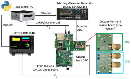
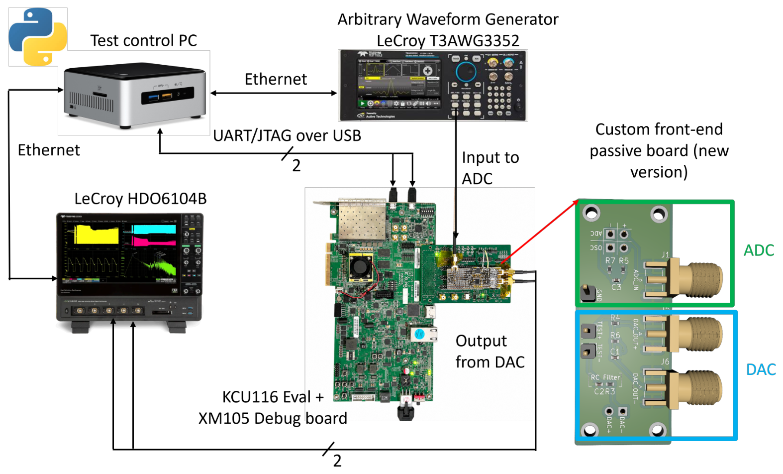
Figure 5 shows the experimental setup used for the ADC/DAC characterization. The system uses an AMD KCU116 evaluation board [25], which hosts a Kintex UltraScale+ FPGA, together with an XM105 FPGA mezzanine card (FMC) debug board [26] and a custom fully passive front-end board. The XM105 provides access to the FPGA I/Os through suitable routed matched traces and serves as the interface between the KCU116 and the external passive circuitry. We used the debug board, as the evaluation board does not offer such differential routing to pin headers. For the ADC, matched connections are used for the ramp-generation signals, whereas the ADC input is driven directly by the external waveform generator. For the DAC, the FPGA output is routed through the passive output-conditioning network, described in Section 2.2, and then to the oscilloscope. The RC networks required for ADC ramp generation and DAC output conditioning were implemented on a piggyback perfboard mounted on the XM105.
Figure 5.
Simplified block diagram of the experimental setup for ADC and DAC characterization.
A LeCroy T3AWG3352 arbitrary waveform generator (Teledyne LeCroy, Chestnut Ridge, NY, USA) provides the ADC test input, while a LeCroy HDO6104B oscilloscope acquires the conditioned DAC output. A test-control PC manages the measurement procedure using Python 3.14.6 control scripts based on the PyVISA library. The PC communicates with the waveform generator and oscilloscope through Ethernet and interfaces with the MicroBlaze processor through the board serial port over USB. We used this setup to calibrate the converters and perform linearity and noise measurements of the implemented system.
3.2. ADC
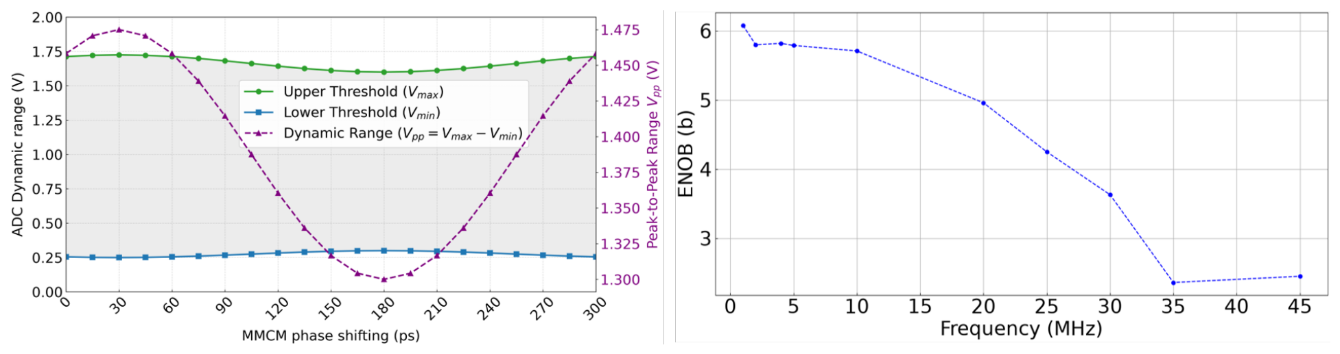
Our architecture requires the RC-shaped ramp-like signal and the TDC clock to be phase-aligned. The FPGA generates 400 MHz clocks for the TDCs and the 200 MHz clock for ramp-like generation by means of a mixed-mode clock manager (MMCM), which multiplies a 300 MHz reference clock from one of the evaluation board oscillators. Since the 200 MHz clock passes through the external RC shaper and re-enters the FPGA, there is a phase difference () between the internal 400 MHz clock and the ramp-like. This in turn reduces the usable portion of the ramp-like for sampling and, consequently, the ADC dynamic range.
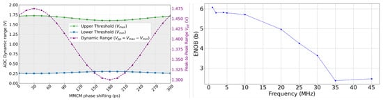
We calibrate using the MMCM fine phase-shifting feature [27], which shifts the generated 200 MHz clock in steps of approximately 15 ps. We perform calibration using an integrated logic analyzer (ILA) configured to acquire 1024 samples from the outputs of the four encoders. We apply a DC voltage to the ADC using the AWG and first set the AWG output to the minimum of the ADC dynamic range. We then shift the MMCM output phase until the encoder output, sampled with the CLK400 clock, reaches 0. We repeat the procedure with the AWG set to the maximum voltage of the ADC dynamic range and record the relevant value from the encoder. We perform the procedure multiple times, confirming consistent values across power cycles. Figure 6 shows how the ADC dynamic range changes with respect to the 200 MHz clock phase shifting by the MMCM.
Figure 6.
(Left), plot of the ADC dynamic range vs the MMCM phase shifting. The phase is correctly aligned when the peak-to-peak voltage () is maximized. (Right), computed ENOB versus frequency for full-scale sinusoidal inputs.
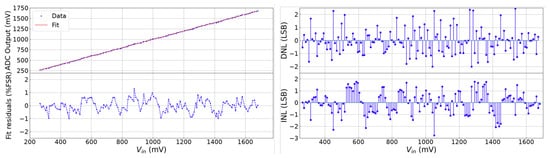
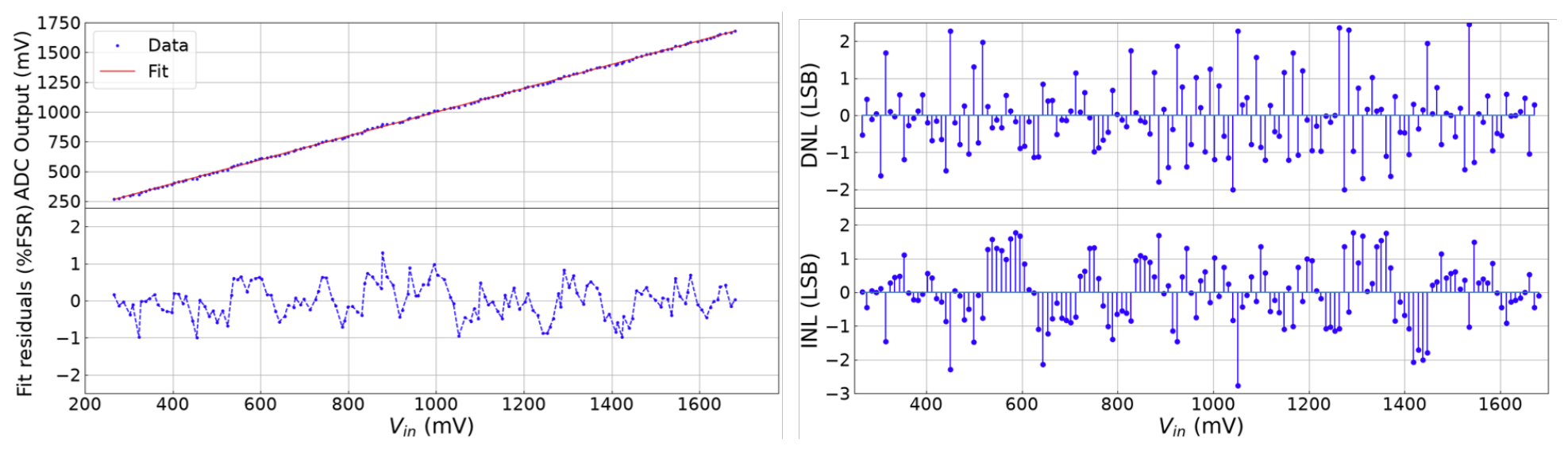
After ADC calibration, we measured the ADC linearity for samples acquired on both the rising and falling slopes of the ramp-like. We performed the calibration in DC; the results are shown in Figure 7. The ADC operates over an input-voltage range from V to V, achieves linearity within 1% over the full range, and shows a gain error of 2.3 LSB. The ADC output is encoded as a 9-bit word, but noise limits its effective resolution to bit in DC. We estimated the ENOB as a function of the frequency of a full-scale sinusoidal input signal. Figure 6 shows the resulting trend, with a clear drop above 10 MHz.
Figure 7.
ADC linearity, taking into account sampling on rise and fall sections of the ramp. (Left), transfer curve with linear fit (top) and corresponding residuals (bottom). (Right), computed differential non-linearity (DNL) (top) and integral non-linearity INL (bottom).
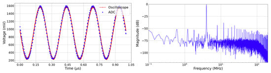
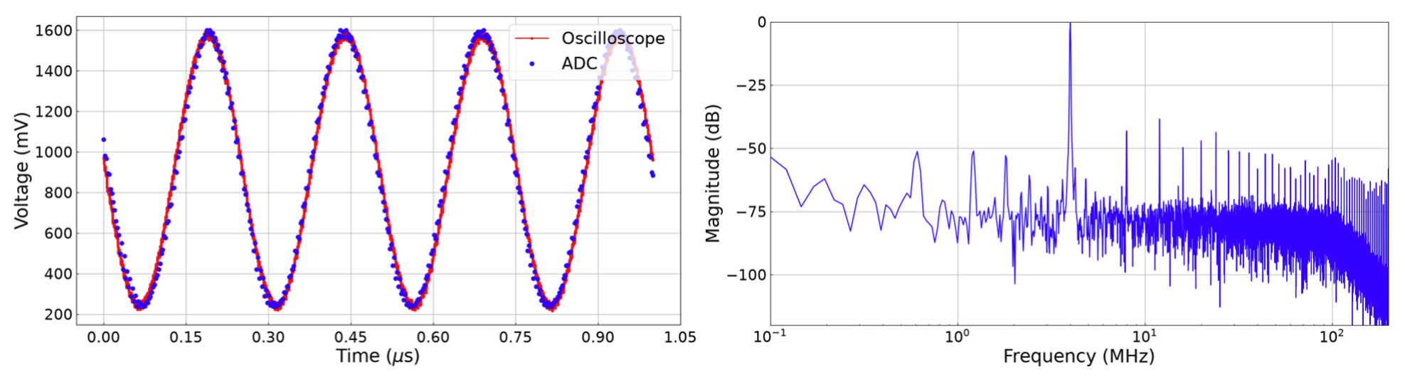
We evaluated the ADC noise performance using a set of test signals. As an example, we report the ADC output for a full-scale, 4 MHz sinusoidal input signal. Figure 8 compares the waveform digitized by the ADC at 400 MSps with the same waveform acquired by the oscilloscope at GSps. We performed a fast Fourier transform (FFT) on the ADC-sampled data, which clearly shows the fundamental component at 4 MHz and noise contributions. With this test signal, the ADC achieves a signal-to-noise ratio (SNR) of dB, a signal-to-noise-and-distortion ratio (SINAD) of dB, a total harmonic distortion (THD) of dB, and an ENOB of bit.
Figure 8.
Example of the ADC sampling a 4 MHz sinusoidal waveform. (Left), comparison between the ADC and an oscilloscope at 2.5 GSps. (Right), FFT of the sampled waveform.
The primary performance boundaries of this ADC design are set by the internal jitter of the clock, the linearity of the generated ramp, and the switching activity of the FPGA logic, which indirectly impacts the threshold uncertainty of the LVDS input comparator. Implementing anti-aliasing filtering or digital noise-shaping mechanisms could further enhance the ENOB, albeit at the expense of additional latency and logic footprint.
To estimate the consumption of our proposed design, we used the AMD Vivado Power Analyzer (Advanced Micro Devices, Inc. (AMD), Santa Clara, CA, USA) at the post-implementation stage. The dynamic power consumption for the implemented ADC design was estimated to be approximately 62 mW. This low-power footprint confirms the suitability of the architecture for multi-channel integration.
3.3. DAC
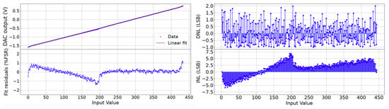
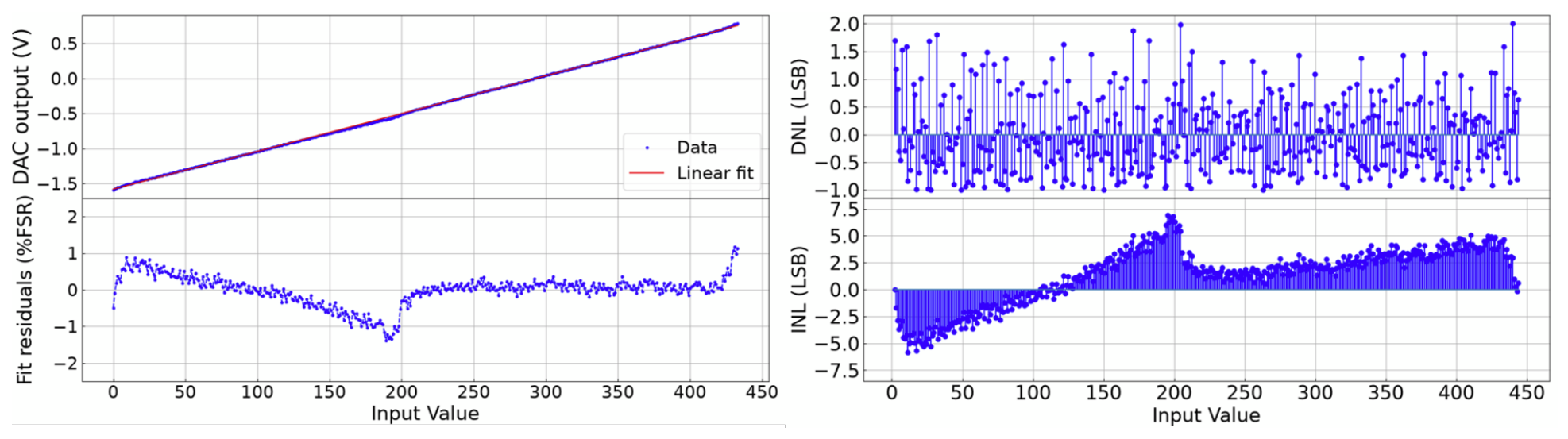
We measured the DAC linearity by sweeping the input word over the full range, and for each DAC input code, measuring the mean output voltage of the waveform sampled by the oscilloscope (Figure 9). The DAC achieves an output range from V to V and an LSB of approximately 5 mV. The non-linearity is bounded within ±2%.
Figure 9.
DAC linearity measurement with linear fit and residuals. (Left), transfer curve with linear fit (top) and corresponding residuals (bottom). (Right), computed DNL (top) and INL (bottom).
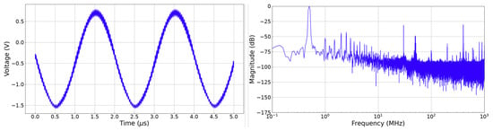
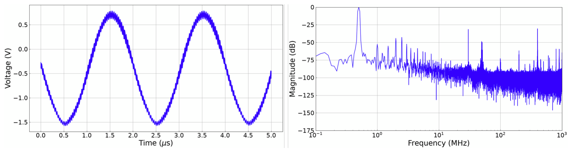
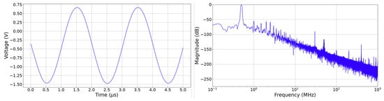
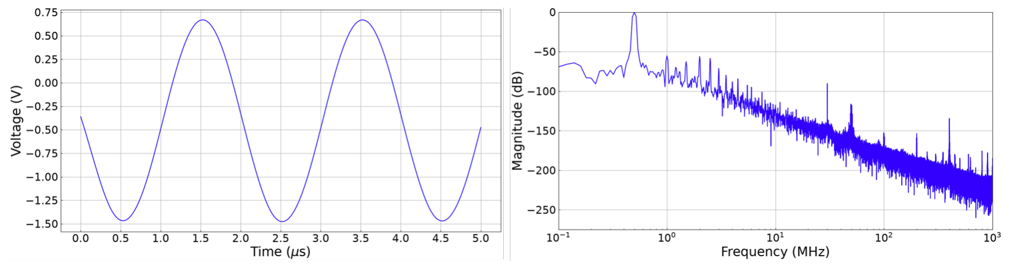
We set our DAC to generate a 500 kHz sine wave, shown in Figure 10, and we computed the FFT on the output acquired by the oscilloscope. We then computed the signal-to-noise ratio (SNR) at 500 kHz, obtaining 25.43 dB, which gives 3.93 ENOB. We measured the input bandwidth of the DAC at −3 dB to be 1.79 MHz. The overall power consumption of the fully digital DAC was estimated to be 194 mW using the Vivado Power Analyzer tool.
Figure 10.
Tests with a 500 kHz sine wave generated by the DAC. (Left), DAC output measured by the oscilloscope. (Right), FFT of the signal.
The limitation of the resolution stems from the significant residual high-frequency switching components (at the 400 MHz carrier frequency) that pass through the simple RC network. To achieve higher dynamic range and ENOB, higher-order passive networks or active filtering topologies are required to provide sharper out-of-band attenuation. However, this introduces a direct trade-off between achievable resolution, physical PCB footprint, and external power dissipation.
In fact, we also explored the possible improvement provided by an additional analog filter at the DAC output, as shown in Figure 11. We selected a second-order Butterworth filter with a cutoff frequency of 1 MHz and implemented it in Python to process the waveform digitized by the oscilloscope. We then repeated our computations obtaining a 50.5-dB SNR and 8.1-bit ENOB. However, this filter reduces the DAC bandwidth to nearly 1 MHz.
Figure 11.
Tests with a 500 kHz sine wave generated by the DAC, filtered using a second-order Butterworth filter implemented in Python. (Left), oscilloscope-acquired DAC output after filtering in Python. (Right), FFT of the filtered signal.
It is important to highlight that the measured performance figures are platform dependent, as carry-chain delay uniformity, clock jitter, and clock distribution skew affect resolution, linearity, and conversion rate, requiring renewed characterization when porting the architectures to other FPGAs or ASICs.
4. Comparison to Relevant Works
Compared with the FPGA-based ADC implementations in Table 2, the proposed design achieves a substantially more compact implementation while maintaining a competitive sampling rate. Relative to [11,12], this work reduces LUT and FF usage by more than 90% and requires significantly fewer carry-chain resources. Compared with [13], the proposed ADC doubles the sampling rate while reducing LUT and FF usage by more than 80% and 60%, respectively. Although the carry-chain resources are not directly comparable, since [13] uses CARRY4 primitives instead of CARRY8 primitives, the proposed design still requires substantially fewer equivalent carry resources. Overall, this work offers a favorable trade-off between sampling rate, conversion performance, and FPGA resources.
Table 2.
Comparison of FPGA-based ADC implementations.
Although the dynamic performance is moderate, with approximately 4 ENOB for the DAC and 6 ENOB for the ADC, the proposed architectures require minimal logic resources and no specialized FPGA primitives. Their compact implementation is particularly suited to low-power, multi-channel detector readout systems, where FPGA resource utilization and power consumption per channel are important design constraints.
The physical implementation and deployment of ADCs and DACs within FPGAs involve trade-offs regarding pin availability, external passive components, and signal integrity.
From an I/O perspective, a single DAC channel requires two output pins. A single-channel ADC requires four pins: two for differential ramp generation and two for the comparator input stage; however, it is reasonable to expect that multi-channel ADCs may share the ramp generator circuit among several inputs. While pin count could be a limitation when scaling to multi-channel architectures on resource-constrained or low-end FPGA devices, modern mid-range FPGAs offer hundreds of I/O pins capable of supporting dozens of ADC/DAC channels (e.g., 64 channels or more).
The proposed FPGA-based DAC offers a favorable combination of I/O efficiency and code-update rate compared with representative FPGA-based DAC architectures. In particular, the all-digital DAC in [14], implemented on an ICE40HX8K FPGA, requires 15 FPGA pins and operates at 20 MSps, whereas the proposed design requires only two pins, accepts a new input code at up to 200 MSps, and generates a 400 MHz PWM output with a measured analog bandwidth of 1.79 MHz. PWM/duty-cycle and sigma–delta implementations can provide higher nominal or in-band resolution [28], while calibrated relaxation-based DACs [29] achieve higher ENOB at substantially lower conversion rates (1–10 kSps). Since these architectures use different modulation frequencies, bandwidths, filters, and characterization methods, their performance values are not always directly comparable. Therefore, the main advantage of the proposed DAC is its combination of high code-update rate, low FPGA-resource utilization, and small output-pin count.
5. Conclusions
We have described two low-footprint FPGA-based data converters for slow-control applications, implemented on an AMD Kintex UltraScale+ FPGA.
The ADC achieves a 1.5 V dynamic range, 9-bit output code width, non-linearity within 1% over the full input range, a DC ENOB of 6.19 bits, and a 400 MSps conversion rate, while requiring only 1943 LUTs, 2556 FFs. A single ADC channel requires two input and two output pins for ramp generation. The output pins can be shared across multiple channels to improve implementation efficiency.
The DAC achieves a 2.3 V dynamic range, an approximately 5 mV LSB, and an ENOB of 3.93 bits for a 500 kHz waveform; it operates at 200 MSps, produces a 400 MHz PWM output and requires about 1011 LUTs, 1444 FFs, and two output pins per channel.
These results support the feasibility of scalable mixed-signal interfaces for front-end electronics implemented in modern FPGAs and pave the way to the implementation in standard-cell ASICs. It is worth remarking that ADC/DAC performance depends on carry-chain uniformity, clock jitter, and skew, requiring re-characterization when porting our solution to other FPGAs or ASICs.
Author Contributions
Conceptualization, R.G. and A.D.N.; methodology, A.D.N., A.B. and R.G.; software, A.D.N.; validation, A.D.N., A.B., J.T. and R.G.; formal analysis, A.D.N. and R.G.; investigation, A.D.N., A.B., J.T. and R.G.; resources, R.G.; data curation, A.D.N.; writing—original draft preparation, A.D.N. and R.G.; writing—review and editing, A.D.N., A.B., J.T. and R.G.; supervision, R.G.; project administration, R.G.; funding acquisition, R.G. All authors have read and agreed to the published version of the manuscript.
Funding
This work is part of the Beyond-CMOS Systems for Fast Machine Learning in Physics project (grant no. 2022XXMTCH), funded by Programma di Ricerca di Interesse Nazionale 2022 of the Italian Ministry of University and Research (MUR), and part of the MEMPHYS project funded by Commissione Scientifica Nazionale 5 of Istituto Nazionale di Fisica Nucleare. Work funded by MUR NextGenEU PRIN2022 E53D23002430006 M4C2.1.1. This work includes the phrasing “Accesso Aperto MUR” as required by MUR.
Data Availability Statement
The data presented in this study are available from the corresponding author upon reasonable request.
Acknowledgments
The authors acknowledge the support of the staff from Servizio Elettronica e Rivelatori of INFN Sezione di Napoli.
Conflicts of Interest
The authors declare no conflicts of interest.
References
- Wang, J.; Hu, X.; Pinkham, R.; Hou, S.; Schwarz, T.; Zhu, J.; Chapman, J.W.; Zhou, B. Fixed-Latency Gigabit Serial Links in a Xilinx FPGA for the Upgrade of the Muon Spectrometer at the ATLAS Experiment. IEEE Trans. Nucl. Sci. 2018, 65, 656–664. [Google Scholar] [CrossRef] [Scilit]
- Yamada, S.; Itoh, R.; Nakamura, K.; Nakao, M.; Suzuki, S.Y.; Konno, T.; Higuchi, T.; Liu, Z.; Zhao, J. Data Acquisition System for the Belle II Experiment. IEEE Trans. Nucl. Sci. 2015, 62, 1175–1180. [Google Scholar] [CrossRef] [Scilit]
- ATLAS Collaboration. The ATLAS Trigger System for LHC Run 3 and Trigger Performance in 2022. J. Instrum. 2024, 19, P06029. [Google Scholar] [CrossRef] [Scilit]
- LHCb Collaboration. The LHCb Upgrade I. J. Instrum. 2024, 19, P05065. [Google Scholar] [CrossRef] [Scilit]
- Aihara, H.; Aloisio, A.; Auguste, D.P.; Aversano, M.; Babeluk, M.; Bahinipati, S.; Banerjee, S.; Barbero, M.; Baudot, J.; Beaubien, A.; et al. The Belle II Detector Upgrades Framework Conceptual Design Report. arXiv 2024, arXiv:2406.19421. [Google Scholar]
- Kim, C.H.; Unno, Y.; Cho, H.E.; Cheon, B.G.; Kim, S.H.; Lee, I.S.; Jang, E.J.; Choi, S.K.; Kim, Y.J.; Ahn, J.K.; et al. Trigger slow control system of the Belle II experiment. Nucl. Instrum. Methods Phys. Res. Sect. A Accel. Spectrometers Detect. Assoc. Equip. 2021, 1014, 165748. [Google Scholar] [CrossRef] [Scilit]
- Kotchetkov, D.; Hartbrich, O.; Andrew, M.; Barrett, M.; Bessner, M.; Bhardwaj, V.; Browder, T.; Cercillieux, J.; Conrad, R.; Danko, I.; et al. Front-end electronic readout system for the Belle II imaging Time-Of-Propagation detector. Nucl. Instrum. Methods Phys. Res. Sect. A Accel. Spectrometers Detect. Assoc. Equip. 2019, 941, 162342. [Google Scholar] [CrossRef] [Scilit]
- Pestotnik, R.; Adachi, I.; Burmistrov, L.; Le Diberder, F.; Dolenec, R.; Hataya, K.; Kakimoto, S.; Kakuno, H.; Kawai, H.; Kawasaki, T.; et al. Front-end electronics of the Belle II aerogel ring imaging detector. Nucl. Instrum. Methods Phys. Res. Sect. A Accel. Spectrometers Detect. Assoc. Equip. 2020, 952, 161711. [Google Scholar] [CrossRef] [Scilit]
- Wu, J.; Hansen, S.; Shi, Z. ADC and TDC implemented using FPGA. In Proceedings of the 2007 IEEE Nuclear Science Symposium Conference Record; IEEE: Piscataway, NJ, USA, 2007; Volume 1, pp. 281–286. [Google Scholar] [CrossRef] [Scilit]
- Wu, J.; Odeghe, J.; Stackley, S.; Zha, C. Improving single slope ADC and an example implemented in FPGA with 16.7 GHz equivalent counter clock frequency. In Proceedings of the 2011 IEEE Nuclear Science Symposium Conference Record; IEEE: Piscataway, NJ, USA, 2011; pp. 2183–2187. [Google Scholar] [CrossRef] [Scilit]
- Leuenberger, L.; Amiet, D.; Wei, T.; Zbinden, P. An FPGA-based 7-ENOB 600 MSample/s ADC without any External Components. In Proceedings of the 2021 ACM/SIGDA International Symposium on Field-Programmable Gate Arrays, FPGA ’21; Association for Computing Machinery: New York, NY, USA, 2021; pp. 240–250. [Google Scholar] [CrossRef] [Scilit]
- Zhang, M.; Zhao, Y.; Chen, Y.; Crovetti, P.; Wang, Y.; Ning, X.; Qiao, S. A 7.4-Bit ENOB 600 MS/s FPGA-Based Online Calibrated Slope ADC without External Components. Sensors 2022, 22, 5852, Erratum in Sensors 2022, 22, 8936. [Google Scholar] [CrossRef] [Scilit] [PubMed]
- Liu, S.; Wu, Z.; Xu, W.; Hu, K. An FPGA-Based ADC Using Multichain Merged Method. IEEE Trans. Nucl. Sci. 2024, 71, 309–315. [Google Scholar] [CrossRef] [Scilit]
- Rueda G., L.E.; Silva, E.; Centeno, A.; Roa, E. All-Digital FPGA-based DAC with None or Few External Components. arXiv 2020, arXiv:2008.00572. [Google Scholar]
- Wirthlin, M. High-Reliability FPGA-Based Systems: Space, High-Energy Physics, and Beyond. Proc. IEEE 2015, 103, 379–389. [Google Scholar] [CrossRef] [Scilit]
- Quinn, H. Radiation effects in reconfigurable FPGAs. Semicond. Sci. Technol. 2017, 32, 044001. [Google Scholar] [CrossRef] [Scilit]
- Kibar, O.O.; Mohan, P.; Rech, P.; Mai, K. Evaluating the Impact of Repetition, Redundancy, Scrubbing, and Partitioning on 28-nm FPGA Reliability Through Neutron Testing. IEEE Trans. Nucl. Sci. 2019, 66, 248–254. [Google Scholar] [CrossRef] [Scilit]
- Scialdone, A.; Ferraro, R.; Alía, R.G.; Sterpone, L.; Danzeca, S.; Masi, A. FPGA Qualification and Failure Rate Estimation Methodology for LHC Environments Using Benchmarks Test Circuits. IEEE Trans. Nucl. Sci. 2022, 69, 1633–1641. [Google Scholar] [CrossRef] [Scilit]
- Giordano, R.; Lai, Y.; Korpar, S.; Pestotnik, R.; Lozar, A.; Šantelj, L.; Shoji, M.; Nishida, S. Frame-Level Intermodular Configuration Scrubbing of On-Detector FPGAs for the ARICH at Belle II. IEEE Trans. Nucl. Sci. 2021, 68, 2810–2817. [Google Scholar] [CrossRef] [Scilit]
- Morabito, M.; Lusardi, N.; Garzetti, F.; Fiumicelli, G.; Bonanno, G.; Ronconi, E.; Costa, A.; Geraci, A. Optimal Implementation of Tapped Delay Line Time-to-Digital Converters in 20 nm Xilinx UltraScale FPGAs. Electronics 2024, 13, 4888. [Google Scholar] [CrossRef] [Scilit]
- Zhu, M.; Qi, X.; Cui, T.; Gao, Q. Tapped delay line for compact time-to-digital converter on UltraScale FPGA and its coding method. Nucl. Instrum. Methods Phys. Res. Sect. A Accel. Spectrometers Detect. Assoc. Equip. 2023, 1056, 168639. [Google Scholar] [CrossRef] [Scilit]
- AMD Inc. UltraScale Architecture Configurable Logic Block (UG574). Available online: https://docs.amd.com/r/en-US/ug574-ultrascale-clb (accessed on 21 July 2025).
- Giordano, R.; Ameli, F.; Bifulco, P.; Bocci, V.; Cadeddu, S.; Izzo, V.; Lai, A.; Mastroianni, S.; Aloisio, A. High-resolution synthesizable digitally-controlled delay lines. IEEE Trans. Nucl. Sci. 2015, 62, 3163–3171. [Google Scholar] [CrossRef] [Scilit]
- Giordano, R.; Cadeddu, S.; Aloisio, A.; Ameli, F.; Bocci, V.; Izzo, V.; Lai, A.; Mastroianni, S. Digitally Controlled Oscillator (DCO) Architecture. WO Patent WO2016071813A2, 12 May 2016. [Google Scholar]
- AMD Inc. Kintex UltraScale+ FPGA KCU116 Evaluation Kit. Available online: https://docs.amd.com/v/u/en-US/ug1239-kcu116-eval-bd (accessed on 21 July 2025).
- AMD Inc. AMD FMC XM105 Debug Card. Available online: https://docs.amd.com/v/u/en-US/ug537 (accessed on 21 July 2025).
- AMD Inc. UltraScale Architecture Clocking Resources User Guide (UG572). Available online: https://docs.amd.com/r/en-US/ug572-ultrascale-clocking (accessed on 21 July 2025).
- Lonla Moffo, B.; Mbihi, J. A Novel Digital Duty-Cycle Modulation Scheme for FPGA-Based Digital-to-Analog Conversion. IEEE Trans. Circuits Syst. II Express Briefs 2015, 62, 543–547. [Google Scholar] [CrossRef] [Scilit]
- Rubino, R.; Crovetti, P.S.; Musolino, F. FPGA-Based Relaxation D/A Converters with Parasitics-Induced Error Suppression and Digital Self-Calibration. IEEE Trans. Circuits Syst. I Regul. Pap. 2021, 68, 2494–2507. [Google Scholar] [CrossRef] [Scilit]

Disclaimer/Publisher’s Note: The statements, opinions and data contained in all publications are solely those of the individual author(s) and contributor(s) and not of MDPI and/or the editor(s). MDPI and/or the editor(s) disclaim responsibility for any injury to people or property resulting from any ideas, methods, instructions or products referred to in the content. |
© 2026 by the authors. Licensee MDPI, Basel, Switzerland. This article is an open access article distributed under the terms and conditions of the Creative Commons Attribution (CC BY) license.