


Abstract
This paper presents an adaptive on-time (AOT) buck converter with a dual-mode zero-current detection (DM-ZCD) scheme for high efficiency over a wide load range. NMOS-switch-based ZCD (ZCD-N) determines whether a transition to discontinuous conduction mode (DCM) is required without periodically activating the freewheeling switch during continuous conduction mode (CCM), and rapidly detects the vicinity of the zero-current crossing (ZCC) during the initial transition from CCM to DCM. The ZCD scheme is then transferred to freewheeling switch-based ZCD (ZCD-F) for accurate ZCC tracking and suppression of switching node ringing in steady-state DCM. During the DCM-to-CCM transition, the absence of a ZCD-F event automatically re-enables ZCD-N circuit. The AOT controller provides near-constant frequency operation in CCM and load-dependent frequency operation in DCM. Dynamic biasing and a subthreshold-biased differential stage reduce control-circuit power consumption and short-circuit current in the comparator output buffer, respectively. Designed in a 0.18-μm CMOS process, the converter operates from a 1.8 V input with a 0.8–1.5 V output and a 10 μA to 700 mA load range. Post-layout simulations predict 98.9% peak efficiency at = 1.5 V and = 10 mA. At a 0.9 V output, peak efficiency is 97.1% and efficiency remains above 90% from 30 μA to 300 mA. The proposed event-based handoff between ZCD schemes enables efficient operation across a wide load range without explicit load current sensing.
1. Introduction
The growing use of data-rich sensors in IoT nodes has intensified the demand for energy-efficient near-sensor processing [1]. Edge computing SoC such as parallel ultra-low-power (PULP) SoC, supports these workloads using near-threshold and parallel processing architectures [2,3,4]. Their load current can vary from several tens of microamperes in deep sleep operation to several hundred milliamperes during computation-intensive operation, requiring a power management buck converter to maintain high efficiency in this wide load range. Under light load conditions, a low switching frequency is required to reduce switching losses, whereas a constant switching frequency is preferred under heavy load conditions to facilitate noise filtering. Since these requirements are inherently achieved by conventional PFM and PWM, respectively, adaptive on-time (AOT) PFM control is attractive because it provides load-dependent switching-frequency operation in light load (DCM) and approximately constant-frequency operation in heavy load (CCM) without an additional selection circuit for the modulation method [5,6,7].
The zero-current detection (ZCD) circuit turns off the low-side NMOS switch () when the inductor current () approaches zero under light load conditions, preventing reverse current and inducing DCM. A conventional NMOS switch-based ZCD, referred to as ZCD-N, directly detects the polarity change of the switching-node voltage (), providing rapid detection [5,6,7,8,9]. However, its detection accuracy is limited by the small on-resistance () of and the small inductor current near the zero-current crossing (ZCC), defined as the instant at which becomes zero. Comparator nonidealities and PVT variations further limit accuracy, and ringing after is turned off degrades the effectiveness of the calibration schemes adopted in [10,11,12,13,14].
A freewheeling switch-based ZCD, referred to as ZCD-F, senses the voltage across the freewheeling switch () after is turned off [15,16]. The larger of increases the accuracy of detection, while prevents the switching node from floating and suppresses ringing. However, ZCD-F relies on iterative tracking of the ZCC and may require several switching cycles to converge after a change in the ZCC. In addition, conventional ZCD-F periodically turns on in CCM to determine whether the converter should enter DCM, thereby reducing CCM efficiency, unlike ZCD-N.
To combine these complementary characteristics, this work proposes a dual-mode-ZCD (DM-ZCD) scheme with an event-based handoff between acquisition and tracking. During CCM and the initial CCM-to-DCM transition, ZCD-N rapidly acquires the vicinity of the ZCC without turning on . Control is then automatically transferred to the ZCD-F, which is based on an analog self-tracking circuit (ASTC), for accurate ZCD in steady-state DCM. During a DCM-to-CCM transition, the absence of a ZCD-F event between consecutive AOT pulses identifies CCM entry, re-enables ZCD-N, and disables ZCD-F by preventing activation. This sequence coordinates the ZCD-N and ZCD-F schemes without the need for direct sensing of the load current.
The main contributions of this work are threefold: first, the proposed handoff separates rapid ZCD-N acquisition from accurate ZCD-F tracking; second, the mode decision circuit and tracking node adjustment in the ASTC support handoff in the ZCD scheme and avoid periodic activation in CCM; third, dynamic biasing and a subthreshold-biased differential output stage reduce control-circuit power consumption and suppress short-circuit current in the following digital buffer. The ASTC and coarse_en generator (CEG) in ZCD-F are adopted from [16], and the AOT control concept and minimum off-time generator are adopted from [7]. For integration with the proposed mode decision circuit, the digital logic of the ASTC and CEG is modified to support handoff between ZCD-N and ZCD-F. In addition, a set-dominant SR latch is employed in the AOT controller, eliminating the need for an additional start-up circuit for the AOT controller. The contribution of this work lies in the handoff between the two ZCD schemes, the mode decision and tracking node adjustment circuits, and the integration of low-power techniques. Designed in a 0.18-μm CMOS process, the converter achieves a post-layout simulated peak efficiency of 98.9%. At = 0.9 V. The peak efficiency is 97.1%, and efficiency remains above 90% from 30 μA to 300 mA.
The remainder of this paper is organized as follows: Section 2 reviews the operating principles and tradeoffs of ZCD-N and ZCD-F as well as the importance of accurate ZCD techniques; Section 3 presents the proposed converter architecture, DM-ZCD handoff sequence, and AOT-PFM operation; Section 4 describes the circuit implementation of the key blocks; Section 5 presents the post-layout simulation results; and Section 6 concludes the paper.
2. Overview and Operating Principles of ZCD Schemes
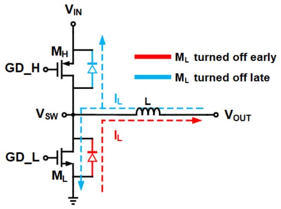
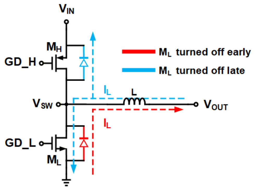
Accurate ZCD is essential for minimizing power loss. As illustrated in Figure 1, late turn-off of causes reverse current, which discharges the output capacitor and subsequently flows through the body diode of , resulting in additional power loss. In contrast, early turn-off causes forward current to flow through the body diode of , resulting in diode conduction loss.
Figure 1.
Mechanism of efficiency degradation due to early or late turn-off of with respect to the ZCC.
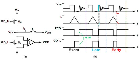
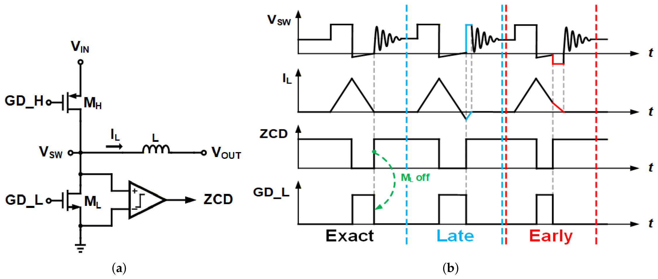
Figure 2 shows the schematic and operating waveforms of ZCD-N. ZCD-N detects the ZCC by directly comparing with ground, and turns off when crosses 0 V. Although this approach enables immediate ZCC detection, its accuracy is limited by comparator non-idealities, propagation delay, PVT variations, and the small of . Adaptive calibration techniques can compensate for these limitations by observing after is turned off [10,11,12,13,14]. However, LC oscillations at the switching node can introduce detection errors and degrade calibration accuracy.
Figure 2.
(a) Schematic and (b) operating waveforms of ZCD-N.
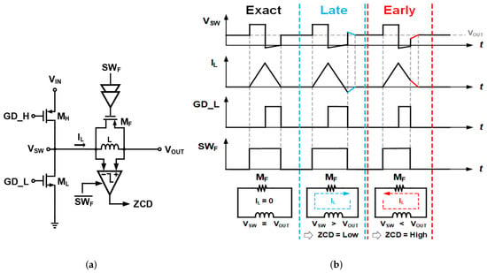
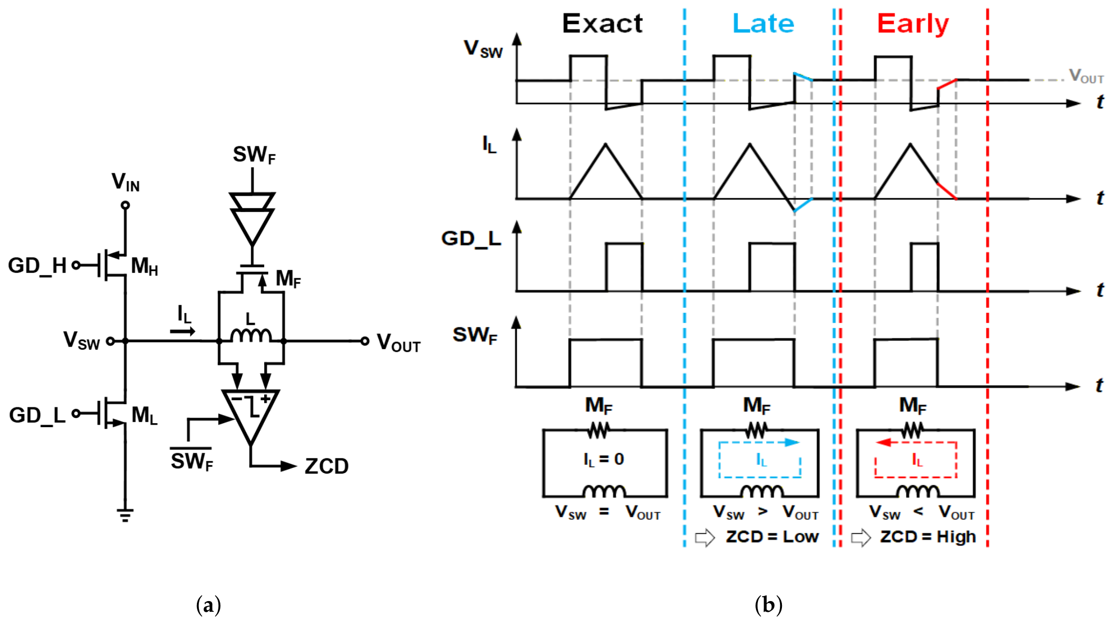
Figure 3 shows the schematic and operating waveforms of ZCD-F. Unlike ZCD-N, which directly detects the ZCC, ZCD-F adaptively tracks the ZCC by evaluating the polarity of the inductor current after is turned off. Specifically, is turned on immediately after is turned off, forming a current path through . If is turned off later than the ZCC, reverse current causes to become higher than and the ZCD output becomes LOW. Conversely, if is turned off earlier than the ZCC, forward current causes to become lower than and the ZCD output becomes HIGH. Based on this information, ZCD-F adaptively adjusts the turn-off timing of toward the ZCC.
Figure 3.
(a) Schematic and (b) operating waveforms of ZCD-F.
Since the of is considerably larger than that of , ZCD-F provides higher detection accuracy than ZCD-N. In addition, prevents the switching node from floating after is turned off, thereby suppressing switching-node oscillations. However, the adaptive tracking operation of ZCD-F requires multiple switching cycles to converge to the ZCC after a ZCC transition, resulting in lower conversion efficiency during the initial tracking period. Furthermore, must be periodically activated even under CCM to determine whether the converter should transition to DCM, resulting in additional CCM power loss.
3. Proposed Structure
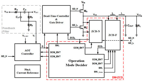
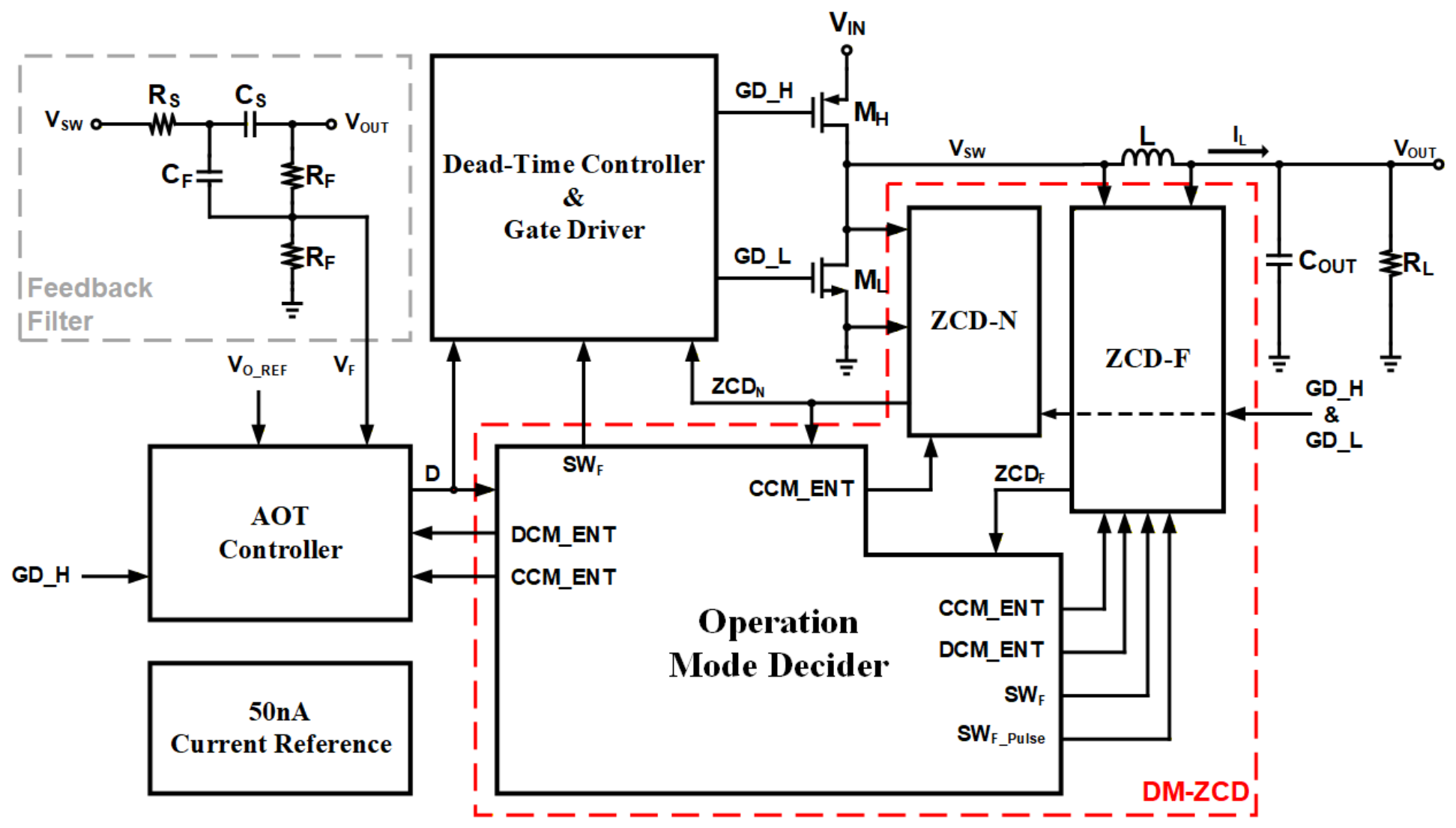
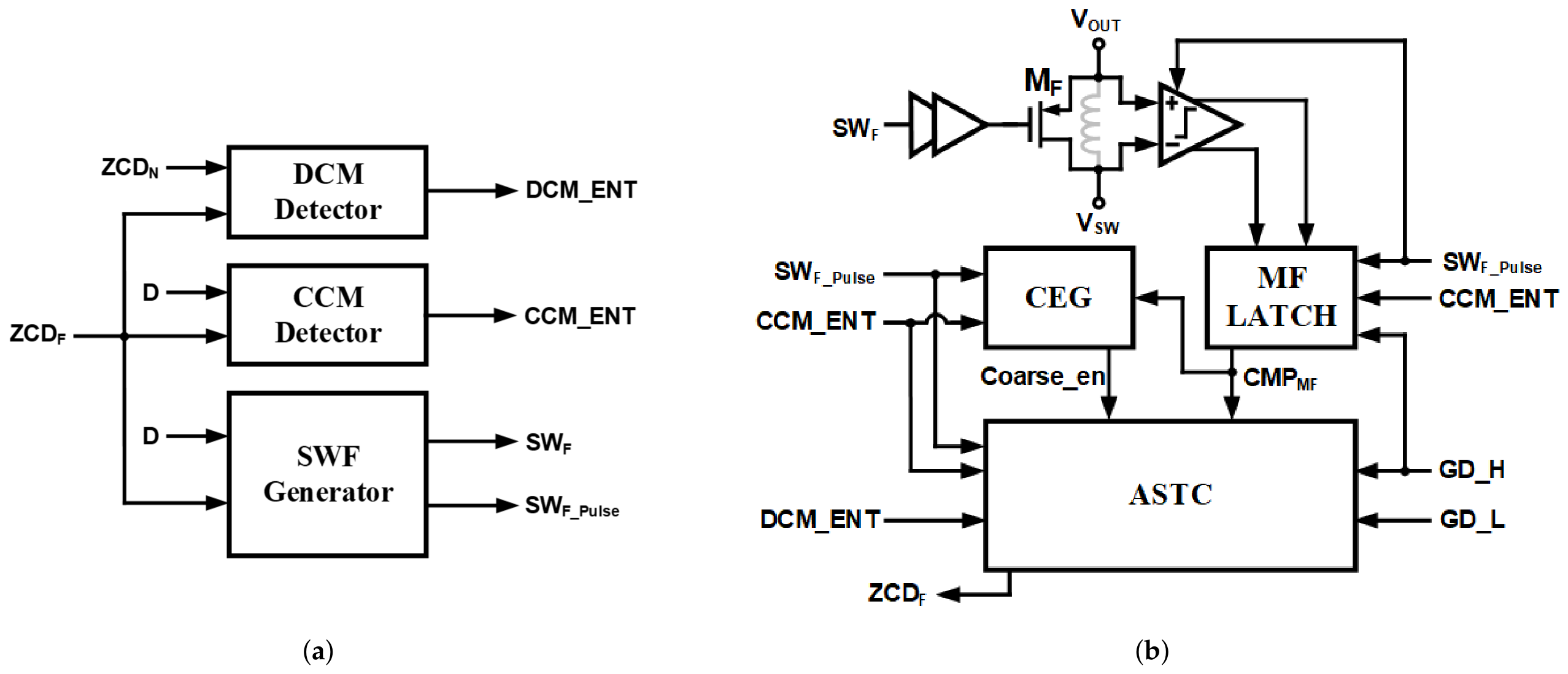
The overall architecture integrating the DM-ZCD and AOT-PFM schemes is shown in Figure 4, while the architectures of the operation mode decider and ZCD-F are shown in Figure 5a,b, respectively.
Figure 4.
The overall architecture integrating the DM-ZCD and AOT-PFM schemes.
Figure 5.
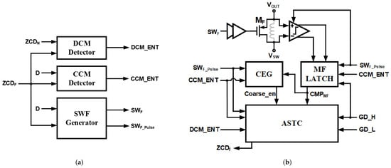
The architectures of (a) the operation mode decider and (b) ZCD-F.
3.1. ZCD-F Operation Based on the ASTC and CEG
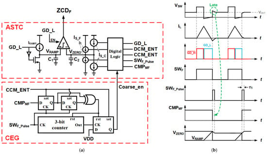
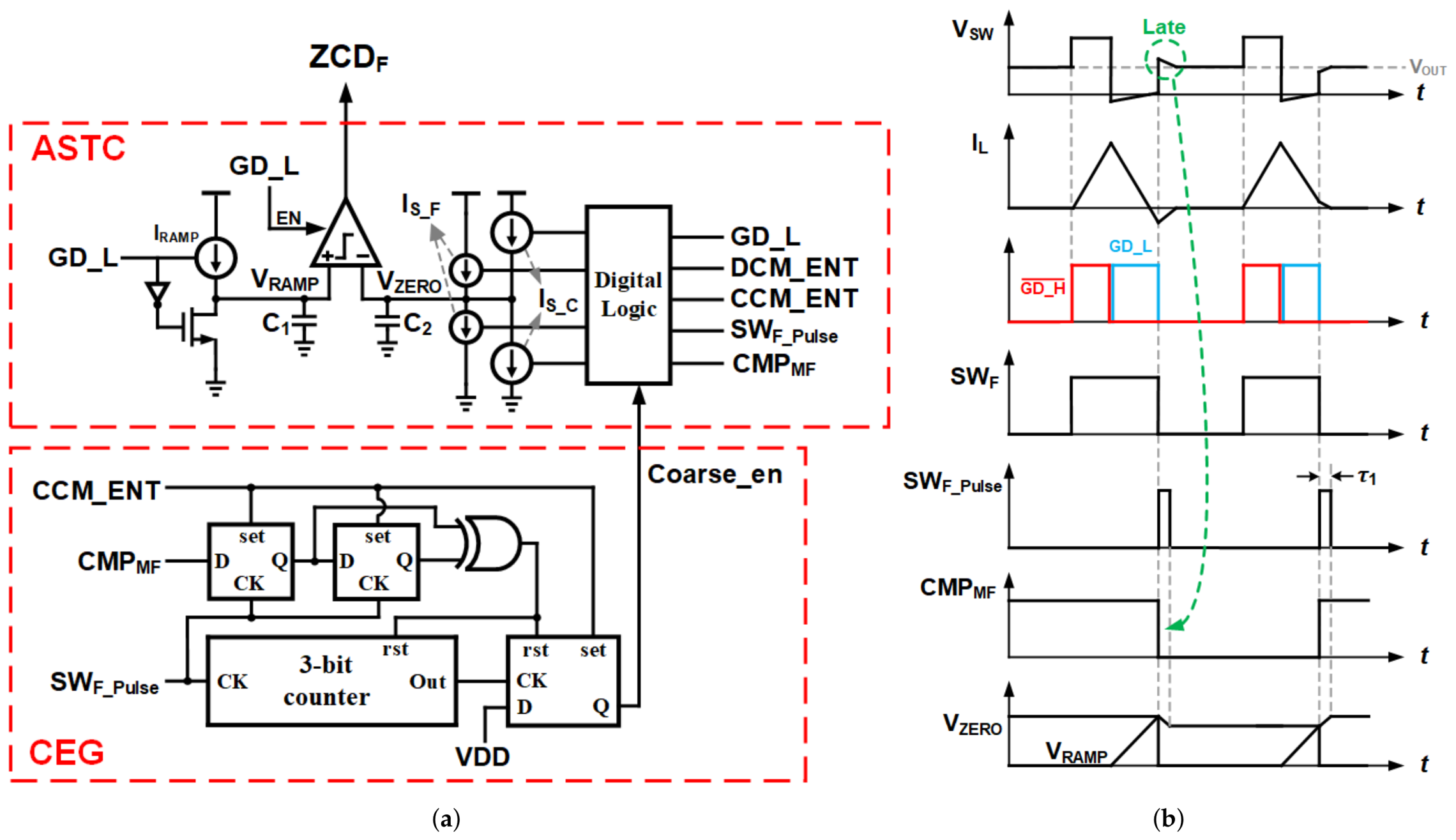
Figure 6a shows the detailed architectures of the ASTC and the CEG embedded in the ZCD-F block, whereas Figure 6b illustrates the operating waveforms of the converter employing the ASTC-based ZCD-F scheme.
Figure 6.
(a) Detailed architectures of the ASTC and the CEG. (b) Operating waveforms of the converter employing the ASTC-based ZCD-F scheme.
The ASTC generates the signal when (which increases with a constant slope while is turned on) intersects with the tracking node . Since the comparator in the ASTC only needs to be activated while is being generated, is employed as its enable signal. The signal serves to pull LOW, thereby turning off and turning on . Subsequently, as described in Section 2, the current loop formed by establishes the relative magnitudes of and . Meanwhile, the signal is generated in response to the falling edge of . The signal is sequentially applied to the MF comparator and its latch, the CEG, and the ASTC through intentionally introduced delays. The MF comparator compares the voltages across .
If is turned off later than the ZCC, becomes higher than , as illustrated in Figure 6b. Upon activation by the signal, the MF comparator detects this condition, causing the output to become LOW. If the converter controlled by ZCD-F is in the steady-state, the discharging fine current source () in the ASTC is subsequently activated for the duration () of the , causing to decrease by a certain amount. Consequently, intersects with earlier than before, resulting in an earlier turn-off of . Conversely, if is turned off earlier than the ZCC and the becomes HIGH, the opposite operation is performed. In this manner, the ASTC technique adaptively adjusts the turn-off timing of , thereby tracking ZCC.
In the steady state, the ZCC remains constant; consequently, repeatedly increases and decreases around its target value. However, when an unexpected disturbance such as noise or leakage occurs, may deviate significantly from its target value, causing the to remain unchanged for several consecutive switching cycles. For example, if is significantly increased by noise, the remains LOW for several consecutive cycles until returns to its target value. Under these conditions, relying solely on causes to decrease slowly, resulting in a slow recovery. Therefore, a CEG and a coarse current source () are introduced.
If the changes, then the output of the XOR gate in the CEG becomes HIGH. In contrast, when the remains unchanged, the XOR gate output remains LOW. While the XOR gate output remains LOW, the 3-bit counter is not reset and continues counting switching cycles. Consequently, after eight consecutive switching cycles without a change in the , the output of the 3-bit counter becomes HIGH, indicating that has deviated significantly from its target value. The output of the 3-bit counter is then used as the clock signal for a D flip-flop (DFF), causing to transition HIGH. Subsequently, while remains HIGH, (which provides a larger current than ) is activated during . As a result, is restored more rapidly. Once returns to its target value, the XOR gate output becomes HIGH, resetting corresponding circuits and driving LOW.
Since the CEG determines whether to activate based on the transition of the , the must be applied to the CEG after the MF comparator updates the state and before the ASTC updates , as described previously. In addition to the operation described above, can also be forced HIGH by the set signal during DCM-to-CCM and CCM-to-DCM transitions. The operation associated with will be described in the following subsection.
The tracking resolution of the ZCC in the ASTC is determined by the minimum produced by the fine current source. In this work, the target tracking resolution is set to be 1 ns. Since the proposed converter is controlled by an AOT controller with a nearly constant switching period around 1 μs in CCM, the maximum duration for which remains HIGH is always shorter than 1 μs, even without imposing a minimum duty cycle. Therefore, the maximum value of -controlled is equal to , since
Considering the 1.8 V supply voltage and the voltage range required to ensure stable current output from the current sources, the maximum value of is chosen to be 1 V. Consequently, the outputs of the current sources and the values of and in ASTC are determined to satisfy and a ramp slope of equal to . The corresponding design equations are given by
where and are the output current of the and , respectively. Based on these equations, , , , , and are chosen as 20 ns, 0.5 μA, 0.5 μA, 0.5 pF, and 10 pF, respectively. Furthermore, the output current of the is chosen to be five times larger than that of the . To summarize, the design parameters are determined sequentially: the target tracking resolution and switching period first determine , while the voltage range required to ensure stable current output determines the maximum . The resulting ramp slope and are then used to determine the current-source output currents , , and using (2) and (3).
The above design is based on a nominal supply voltage of 1.8 V. When the supply voltage changes within a range where the current sources can maintain stable output currents over the selected range, the design parameters do not need to be recalculated; otherwise, the range should be reconsidered to ensure stable current-source operation and the subsequent design parameters should be recalculated accordingly.
3.2. Operating Principle of the Proposed DM-ZCD
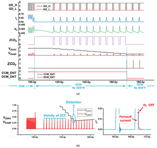
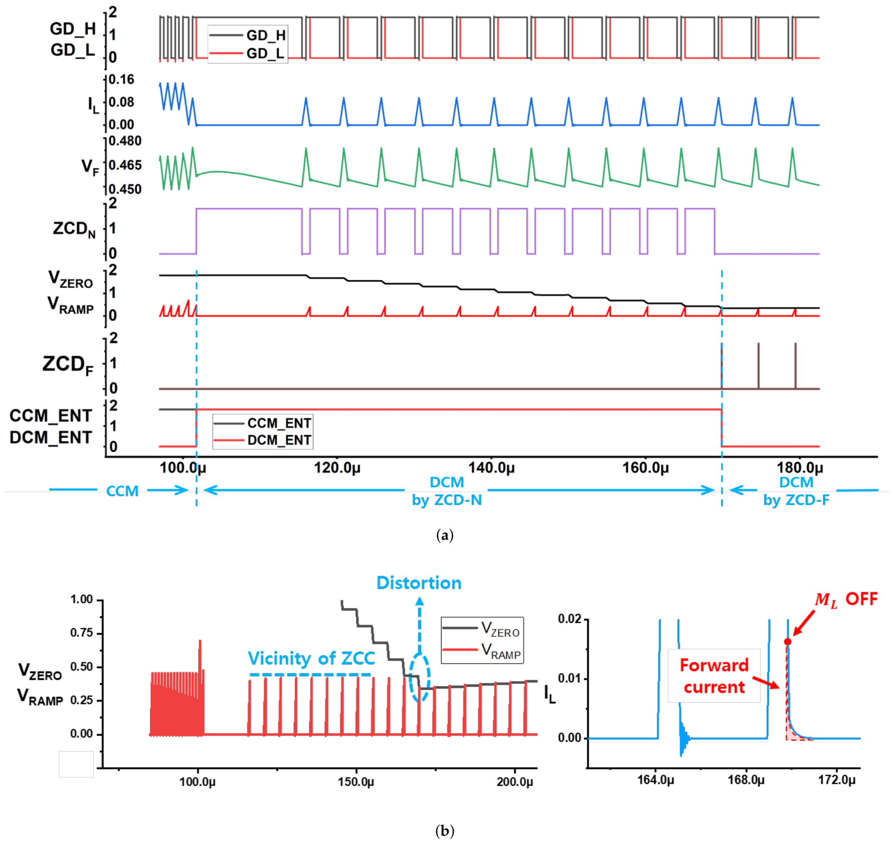
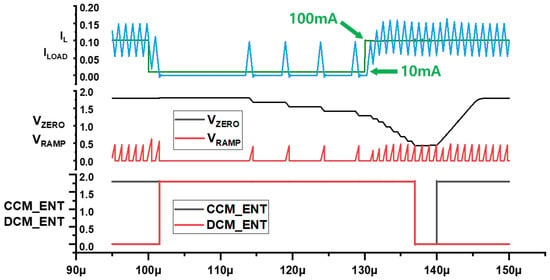
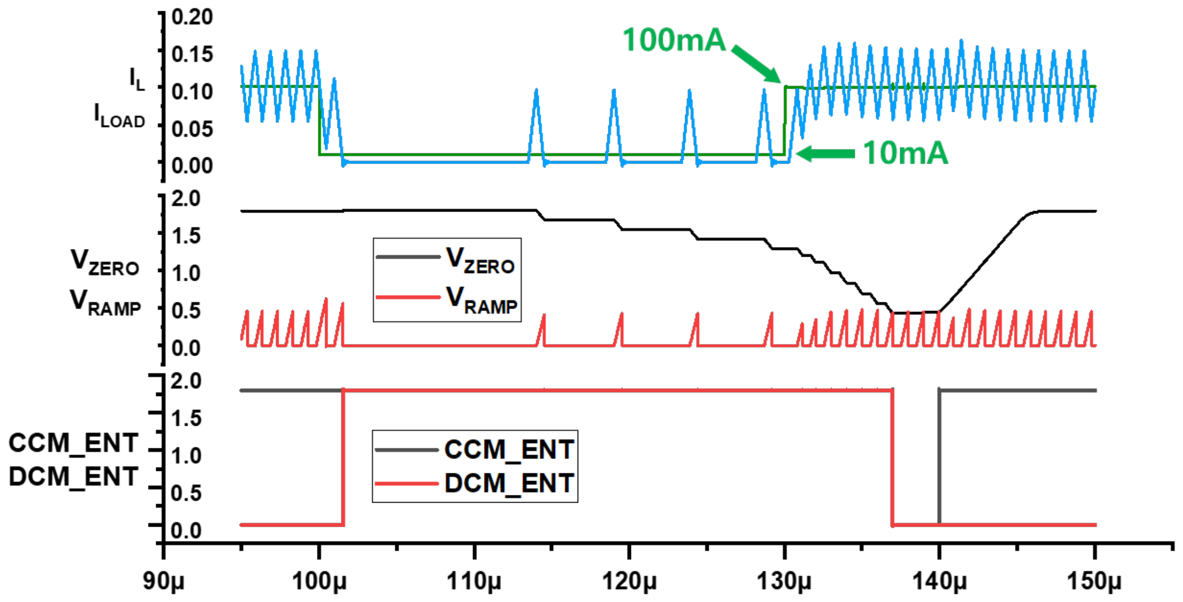
Figure 7a shows the operating waveforms of the overall architecture presented in Figure 4 during a heavy-to-light load transition from 100 mA to 10 mA with a load-current transition time of 10 ns at V. During CCM operation, remains at ; therefore, it does not intersect with , preventing turn-on of and avoiding CCM efficiency degradation.
Figure 7.
(a) Operating waveforms during a heavy-to-light load transition from 100 mA to 10 mA with a load-current transition time of 10 ns at V and (b) distortion of the vicinity of ZCC.
When the decreases below zero due to a heavy-to-light load transition, ZCD-N turns off by driving HIGH, thereby enabling immediate detection of the ZCC and recognizing the need to transition into DCM. Subsequently, the converter operates in DCM under the control of ZCD-N for several periods. Because is controlled by the signal, the instant at which goes LOW, i.e., the vicinity of ZCC, is captured by during these periods.
The rising edge of causes the DCM detector in the operation mode decider to drive HIGH. Upon this high signal, , which had previously remained at , is gradually discharged by and whenever goes HIGH. As intersects with , goes HIGH, thereby driving LOW and stopping the gradual discharge of . Through this operation, the DM-ZCD switches the ZCD mechanism from ZCD-N to ZCD-F.
The number of switching cycles required for this handoff depends on the VCR because the amount by which is discharged in each switching cycle is determined by the duration for which remains HIGH. Since this duration increases as the VCR decreases, the required handoff duration ranges from 10 to 33 switching cycles over the designed output-voltage range, with 10 cycles at V and 33 cycles at V.
During the transition from ZCD-N to ZCD-F, suppresses the peak of , causing the vicinity of ZCC previously captured by ZCD-N to be distorted. Consequently, ASTC turns off earlier than the ZCC, inducing a large forward current, as illustrated in Figure 7b. In the worst-case condition, the peak of is suppressed by approximately 90 mV, resulting in a forward current of up to approximately 22 mA.
To recover rapidly from this distortion, the signal preemptively forces both and HIGH through the latch and the CEG, respectively. With this forced-coarse mechanism, the converter recovers from the distortion within 14 switching cycles, corresponding to 65.8 μs when mA. Without the forced-coarse mechanism, the recovery would require approximately 20–21 switching cycles, as must wait until rises consecutively for eight cycles to become HIGH. The implementation of the forced-coarse mechanism using the latch is described in Section 4, Circuit Implementation.
In ZCD-N-controlled DCM, must remain HIGH to force HIGH, enabling the gradual discharge of and rapid recovery from distortion. In contrast, in ZCD-F-controlled DCM, must be driven LOW to disable the forced HIGH state of , thereby preserving the intended resolution of . Therefore, the LOW-to-HIGH transition of drives LOW in addition to . Furthermore, since the period during which remains HIGH exactly corresponds to the period in which ZCD-N operation is required, can be used as the enable signal for ZCD-N, thereby avoiding unnecessary power consumption.
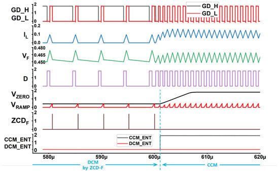
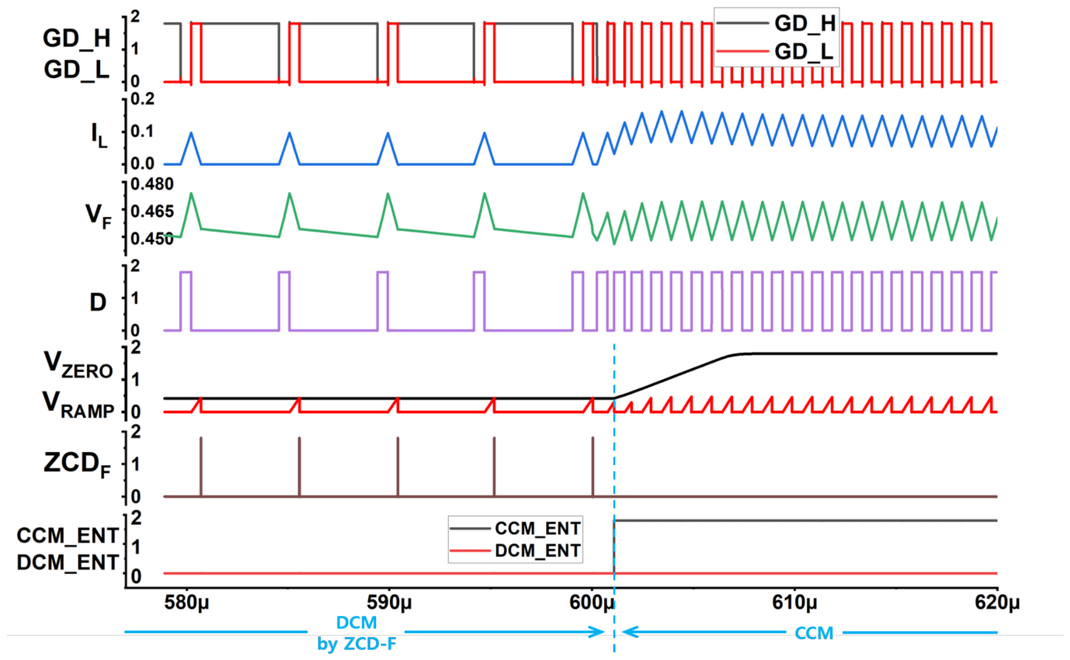
The operating waveforms during a light-to-heavy load transition from 10 mA to 100 mA with a load-current transition time of 10 ns at V are shown in Figure 8. During ZCD-F-controlled DCM, one event is expected between consecutive rising edges of the AOT controller output D, where each rising edge corresponds to the turn-on of . If the next rising edge of D occurs without an intervening event, this indicates that the converter has entered CCM, and the CCM detector in the operation mode decider drives HIGH. Upon going HIGH, is charged to by to prevent from intersecting with , thereby avoiding the turn-on of during CCM. In addition, ZCD-N is re-enabled to monitor whether the inductor current reaches zero. This event-based decision identifies CCM entry without explicit load current sensing.
Figure 8.
Operating waveforms during a light-to-heavy load transition from 10 mA to 100 mA with a load-current transition time of 10 ns at V.
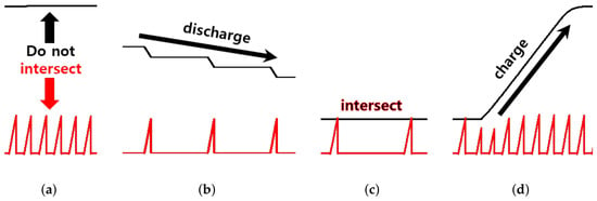
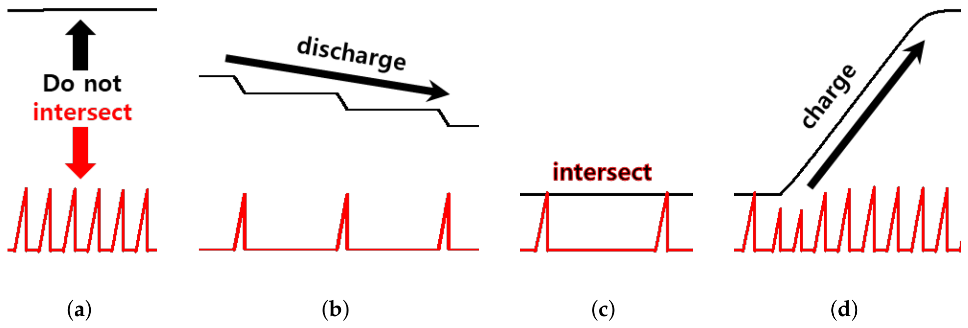
In summary, the converter operates in CCM (, ), ZCD-N-controlled DCM (, ), or ZCD-F-controlled DCM (, ). To realize these operating modes, is appropriately charged or discharged by the digital control logic in the ASTC, as shown in Figure 9. The corresponding logic is summarized in Table 1.
Figure 9.
Characteristics of (black) and (red): (a) CCM, (b) ZCD-N-controlled DCM, (c) ZCD-F-controlled DCM, and (d) DCM-to-CCM transition.
Table 1.
Digital control logic for in the DM-ZCD.
Consequently, the proposed DM-ZCD employs an event-based handoff between rapid ZCD-N acquisition and accurate ZCD-F tracking. Specifically, during CCM or the initial stage of the CCM-to-DCM transition, ZCD-N enables reverse-current detection without turning on and provides rapid detection of the ZCC. Subsequently, in the steady state of the DCM, ZCD-F provides high accuracy in detecting the ZCC while eliminating switching-node oscillations. As a result, the proposed DM-ZCD enables efficient operation over a wide load range covering both CCM and DCM. Furthermore, because the operating mode can be uniquely identified from the states of and , the proposed DM-ZCD also provides the flexibility to incorporate additional functions based on these mode indicator signals.
As an additional observation, Figure 10 shows the waveforms under a back-to-back load step, where the load returns to a heavy load condition during the handoff from ZCD-N to ZCD-F caused by a heavy-to-light load transition. In this case, although the converter has already returned to CCM, both and remain HIGH while is discharging. Subsequently, and briefly intersect, after which is charged back to and the relevant control signals again indicate CCM operation. Although the turn-on of during the brief intersection of and causes additional power loss, this condition persists for only a few switching cycles, after which all mode-related signals indicate CCM operation. Therefore, the proposed handoff mechanism can robustly recover from back-to-back load transients without remaining in an incorrect operating state.
Figure 10.
Waveforms under back-to-back load steps: 100 mA to 10 mA and 10 mA to 100 mA.
3.3. Operating Principle of the AOT-PFM Control
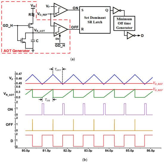
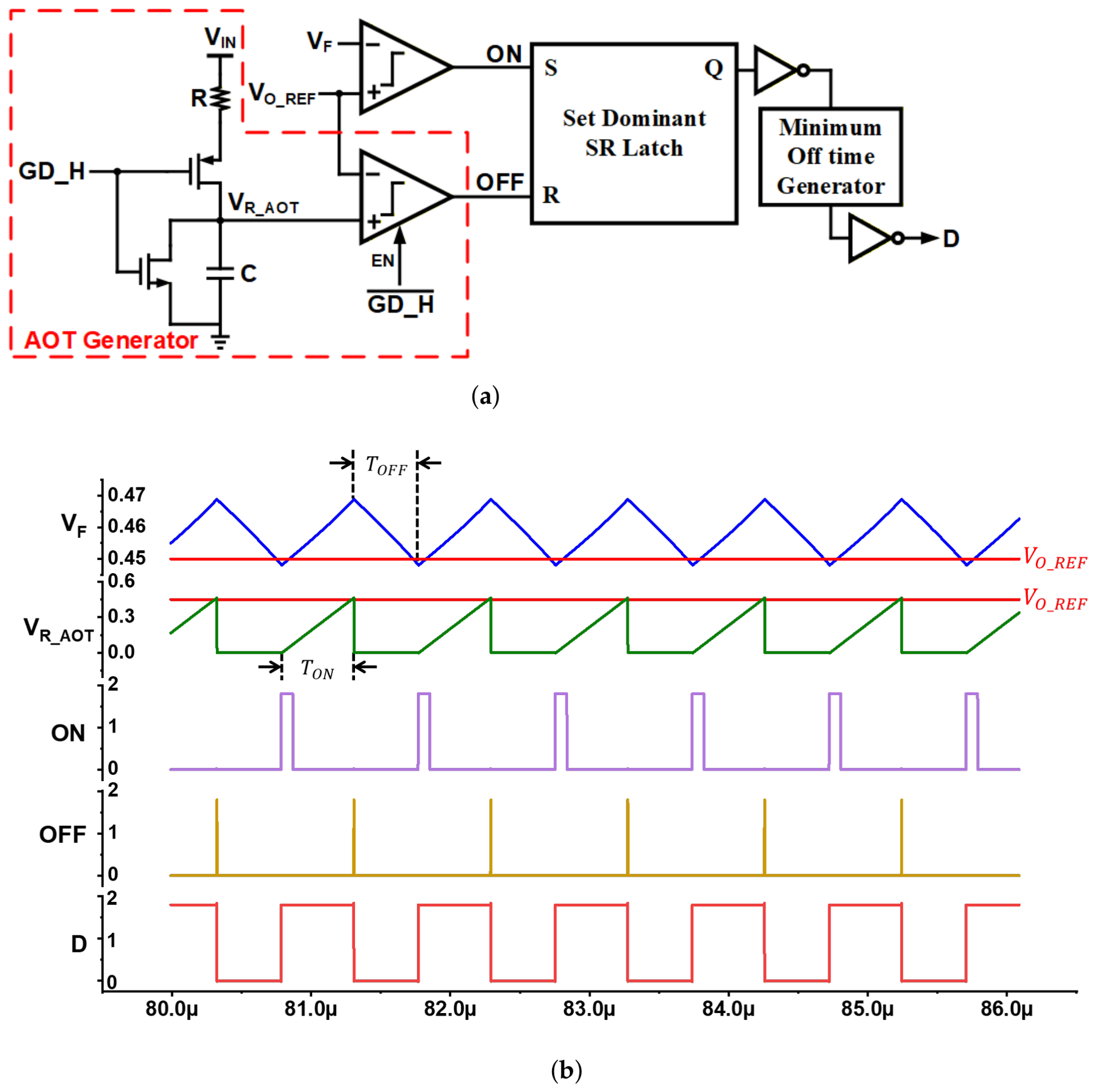
The structure and operating waveforms of the AOT controller during CCM are shown in Figure 11a,b, respectively. The ON time () is determined by the time required for the generated by the AOT generator to increase to . In contrast, the OFF time () is determined by the time required for the feedback signal (), which is in phase with , to decrease to . Accordingly, the ON time is adaptively determined by the AOT generator based on . Since the comparator in the AOT generator only needs to be activated while the ramp signal of is being generated, i.e., when is LOW, is employed as its enable signal to reduce unnecessary power consumption.
Figure 11.
(a) Structure and (b) operating waveforms of the AOT controller.
The slope of generated by the resistor and capacitor in the AOT generator is given by . In addition, as shown in Figure 4, the DC level of is set to by the voltage divider formed by in the feedback filter. Therefore, the reference voltage satisfies . Accordingly, the in CCM can be derived as
Since the target in CCM determined by the AOT controller is 1 MHz, R and C in the AOT generator are chosen as and , respectively. As a result, the in CCM is determined solely by the values of R and C without requiring an additional clock signal. Accordingly, the converter operates similarly to PWM mode with a nearly constant of approximately 1 MHz in CCM while operating in PFM mode with a load-dependent in DCM, without the need for an additional modulation method selection circuit. The relationship between in DCM and the load current can be expressed as follows:
where denotes the difference between immediately after is turned off and the target . As indicated by (6), increases as the load current decreases, resulting in a lower switching frequency at light loads. Consequently, the switching loss is reduced at light loads, enabling efficient operation over a wide load range.
The simulated minimum on-time is approximately 36 ns, and is primarily limited by the delay of the comparator employed in the AOT generator; the minimum off-time is approximately 32 ns and is determined by the minimum off-time generator. For the nominal CCM switching period of 1 μs, these values correspond to an achievable duty cycle range of approximately 3.6%–96.8%. In addition, these minimum on- and off-times impose a theoretical upper bound of approximately 14.7 MHz on the switching frequency which is well above the designed CCM switching frequency of approximately 1 MHz.
As shown in Figure 11a, the use of a set-dominant SR latch, which forces the output to the set state under the forbidden input condition, eliminates the need for an additional start-up circuit for the AOT controller, unlike the design in [7]. The operating states of the AOT-PFM converter according to the relative magnitudes of the compared voltages are summarized in Table 2.
Table 2.
Operating states of converter employing the proposed AOT controller.
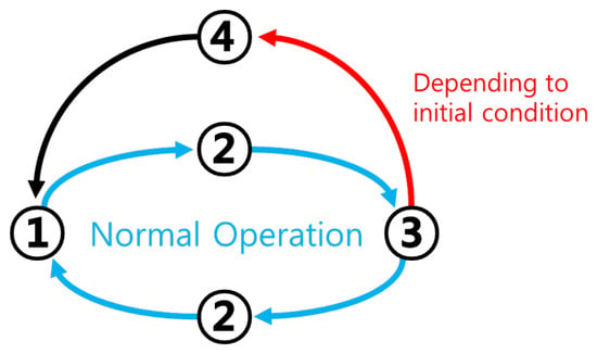
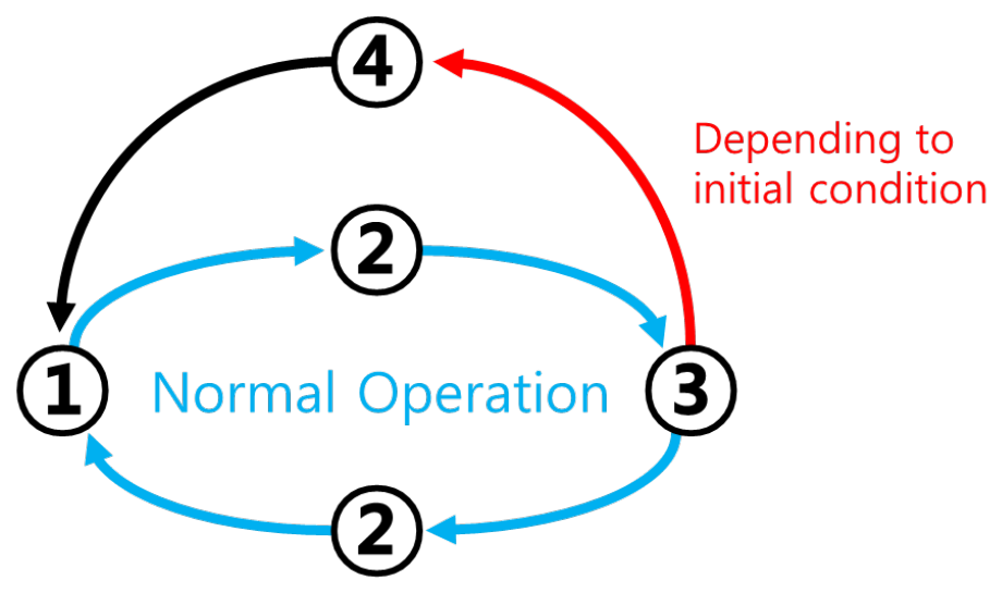
When the converter enters State 1, the discharge NMOS in the AOT generator immediately discharges to 0 V, causing the converter to transition to State 2. Subsequently, as continues to decrease, the converter enters State 3. Under normal operation, once State 3 is reached, immediately becomes greater than , returning the converter to State 2. Thereafter, as continues to increase, the converter transitions back to State 1.
However, depending on the initial conditions of the converter, the converter may transition from State 3 to State 4. During the start-up phase, this transition occurs if exceeds before exceeds . In State 4, the set-dominant SR latch forces D to remain HIGH. Consequently, both and continue to increase until exceeds , at which point the condition for State 4 is no longer satisfied and the converter transitions to State 1. The resulting state transitions are illustrated in the state diagram shown in Figure 12. Therefore, regardless of the initial conditions under which the converter starts operating, the converter always converges to the normal operation.
Figure 12.
State diagram of converter employing the proposed AOT controller.
4. Circuit Implementation
4.1. Operation Mode Decider and ZCD-N
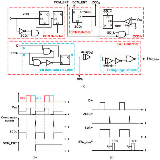
The detailed implementation of the operation mode decider and ZCD-N is shown in Figure 13a. These circuits generate the operation-mode control signals ( and ) as well as the signals used to turn off ( and ).
Figure 13.
(a) Detailed implementation of the operation mode decider and the ZCD-N, (b) operating waveforms of the ZCD-N and the DCM detector, and (c) operating waveforms of the SWF generator.
First, the operating waveforms of the ZCD-N and the DCM detector are shown in Figure 13b. The operating concept of the ZCD-N and the schematic of its internal comparator are adopted from [7]. The comparator in the ZCD-N compares with ground and outputs a HIGH when becomes positive. This output is used as the clock signal for a DFF, causing to be driven to (HIGH). The comparator is enabled only when both and are HIGH. Therefore, once becomes HIGH and turns off , the comparator is immediately disabled, forcing its output LOW. In this manner, the comparator is activated only when required, thereby reducing unnecessary power consumption. Subsequently, at the beginning of the next switching cycle, is reset to LOW by the LOW of . The DCM detector following the ZCD-N detects the rising edge of and drives to (HIGH). Afterward, when high is detected, becomes LOW to switch the ZCD scheme.
Next, the operating waveforms of the SWF Generator are illustrated in Figure 13c. Here, D and serve as the set and reset signals, respectively. When D becomes HIGH (that is, when is turned on), is driven to HIGH, turning off ; conversely, when becomes HIGH, is driven LOW, thereby turning on and turning off . However, if turns off at almost the same time that would normally be turned off without ZCD circuit, then the HIGH of D and may occur simultaneously, since D is the signal before the gate driver delay. Since this forbidden input condition of the SR latch is reasonably interpreted as CCM operation, a set-dominant SR latch is adopted.
When is driven to LOW, a falling edge detector generates . is generated from the -delayed to compensate for the RC delay caused by the of and the parasitic capacitance at the switching node, which slows the rise of toward the vicinity of the level after is turned off. Consequently, the delay allows and to be compared after their voltage relationship is determined solely by the forward or reverse current, ensuring accurate ZCD-F operation.
The CCM detector is implemented by cascading two DFFs using D as the clock signal and as the reset signal. During ZCD-N operation, the event drives LOW, thereby switching the ZCD scheme to ZCD-F. During ZCD-F operation, one event is expected between two consecutive rising edges of D, and remains LOW; otherwise, is driven to (HIGH), switching the operation mode to CCM. As mentioned previously, in order to interpret the simultaneous HIGH of D and as CCM operation, an AND gate combines and .
4.2. Latch of MF Comparator
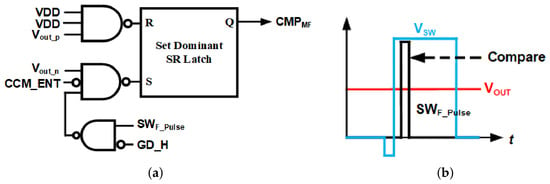
In Section 4.1, the simultaneous HIGH of and D was addressed. A similar consideration must also be applied to the latch of the MF comparator (hereafter referred to as the MF latch). In addition, to mitigate the distortion shown in Figure 7b, the MF latch is required to output when is HIGH. Accordingly, the MF latch is designed as shown in Figure 14a.
Figure 14.
(a) Detailed implementation of the MF latch and (b) the case where and become HIGH simultaneously.
Since is generated with a delay of from the falling edge of , the HIGH of and may still occur simultaneously despite the solution introduced in Section 4.1. As illustrated in Figure 14b, under this condition, the MF comparator performs the voltage comparison only after has risen to due to the turn-on of . Consequently, the MF comparator outputs even though the converter should be operating in CCM, causing to decrease and creating a condition in which can be turned on. As shown in Figure 14a the MF latch is designed to prevent this behavior, such that whenever and become HIGH simultaneously, is driven to HIGH regardless of all other input signals. Likewise, when is HIGH, the MF latch forces HIGH regardless of the other inputs in order to mitigate the distortion shown in Figure 7b.
Even after incorporating the above functions, the circuit must still operate as a latch under normal comparison conditions. The MF comparator, implemented as a StrongARM Latch [17], outputs in its idle state. Furthermore, a NAND gate functions as an inverter when its other input remains HIGH. Taking these characteristics into account, and are applied to the positive and negative inputs of the MF comparator, and , respectively. Its positive and negative outputs, and , respectively, are then connected to the MF latch, as shown in Figure 14a. Consequently, as shown in Table 3, the proposed MF latch performs the intended logic.
Table 3.
Operation of the proposed MF latch under normal comparison conditions.
4.3. Comparator
To identify the dominant power-consuming circuits, the power consumption of each block and circuit in the proposed converter must first be examined. Although the ASTC includes several current sources, their output currents are small and they are activated only temporarily. Consequently, as the load current decreases and the switching period becomes longer under PFM control, their contribution to the total power consumption is progressively reduced. The MF comparator is a dynamic comparator that consumes only dynamic power. The comparators employed in the ASTC and the AOT generator are activated only when and are turned on, respectively. Therefore, the power consumption of these three comparators also becomes less significant as the load current decreases. The comparator used in the ZCD-N is not activated during DCM operation controlled by the ZCD-F, and so consumes no power under steady-state DCM operation.
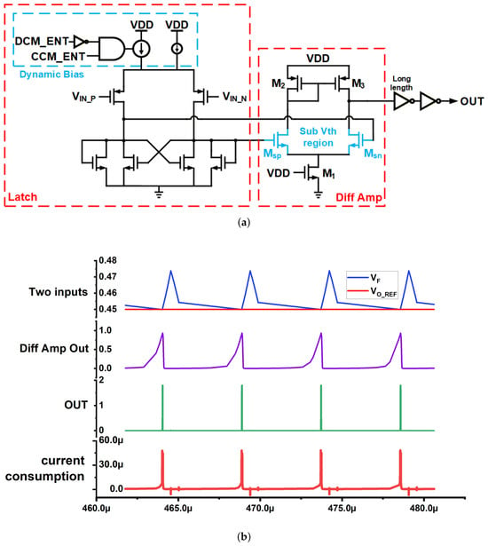
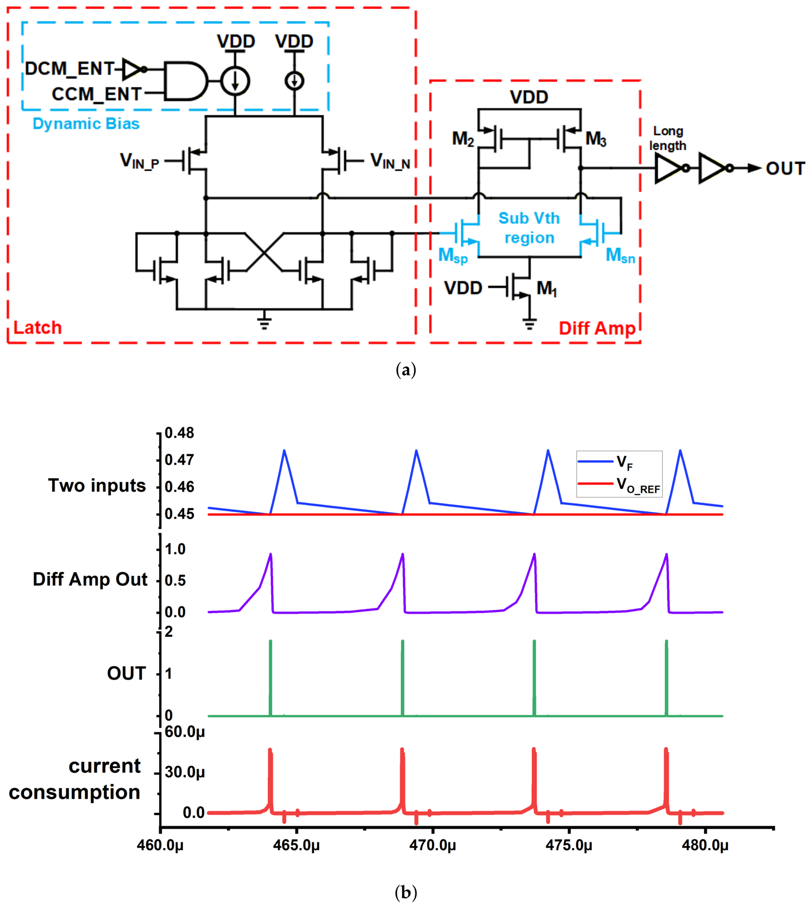
In contrast, the static comparator that compares with in the AOT controller (hereafter referred to as the AOT comparator) must remain continuously active; therefore, minimizing the power consumption of this comparator is of particular importance. Reducing the bias current of the comparator is essential for lowering its power consumption. However, another important issue must also be considered: if the two input voltages of the comparator are very close, the output voltage may remain at an intermediate level for a long time, allowing short-circuit current to flow in the subsequent digital buffer, thereby increasing power consumption. This issue is particularly critical for the AOT comparator, since the difference between and is typically within 20 mV.
A straightforward solution is to employ a differential amplifier as the second stage of the comparator. However, the static bias current required by a conventional differential amplifier can become a significant power overhead under light load conditions. To address this issue, the proposed design adopts a differential amplifier with input transistors that operate in the subthreshold region (hereafter referred to as the diff amp), as shown in Figure 15a.
Figure 15.
(a) Schematic of the proposed AOT comparator and (b) its operating waveforms at V and = 10 mA (DCM).
The first stage latch serves two purposes: it enlarges the input voltage difference of the second stage relative to that of the latch, and it ensures that and operate in the subthreshold-region during DCM. A dynamic bias scheme is adopted for the latch such that the left bias current is enabled only during CCM. Consequently, the bias current of latch is 2 μA in CCM and 0.3 μA in DCM.
Next, consider the second stage, namely, the diff amp. Both and operate in the subthreshold region, while the drain voltage of is pulled close to 0 V by the of and , forcing to operate in the deep triode region. As a result, the diff amp consumes only several tens of nanoamperes when the input voltage difference is relatively large and several hundreds of nanoamperes when the two inputs are close to each other. Since this circuit functions as a comparator, its output common-mode voltage should be approximately . Therefore, and are designed with long channel lengths.
As a result of these design techniques, the operation of the AOT comparator is illustrated in Figure 15b. The diff amp ensures that its output does not exceed 0.5 V unless the voltage difference between two inputs of the AOT comparator is within 0.5 mV, thereby suppressing short-circuit current in the subsequent buffer. In addition, the first inverter in the digital buffer is implemented with a long channel length to reduce the short-circuit current. Consequently, the current consumption of the AOT comparator exhibits a brief peak when the two input voltages become nearly identical, then returns to the bias-current level discussed above. Owing to the characteristics of PFM control, the interval between these current peaks increases as the load current decreases, resulting in a lower average current consumption of the AOT comparator.
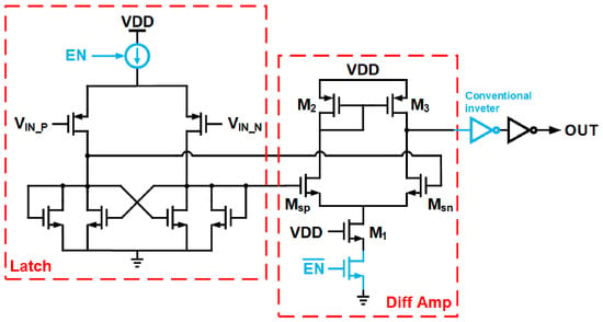
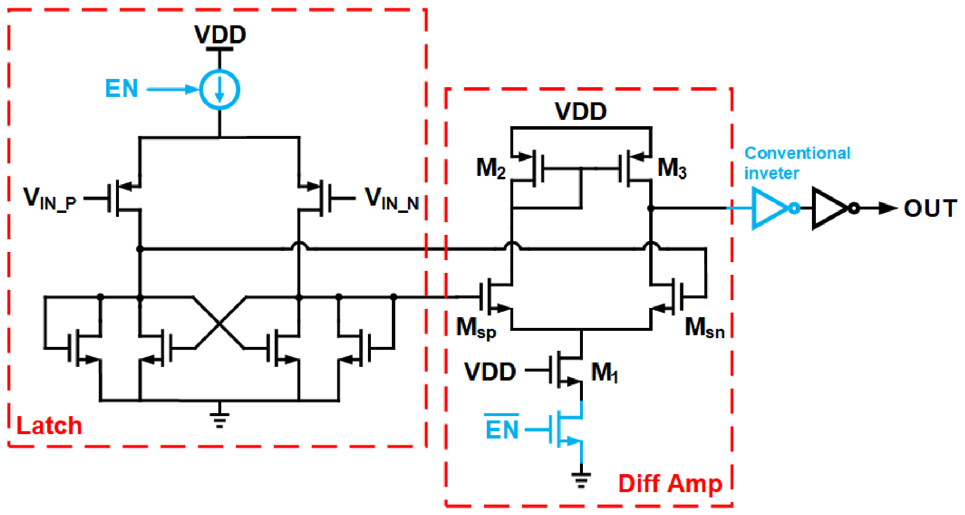
The comparators employed in the ASTC and the AOT generator are designed based on the same principle, as shown in Figure 16. However, because these comparators are activated only when an enable signal becomes HIGH, several modifications are introduced. In the first stage, the dynamic bias current range of 0.3–2 μA is changed to 0–2 μA. In the second stage, an additional NMOS transistor controlled by the enable signal is inserted below to provide the enable function. Furthermore, the long channel inverter is replaced with a conventional inverter.
Figure 16.
Schematic of the comparators employed in the ASTC and AOT generator, with the modified components highlighted in blue.
Under the same comparison conditions with a conventional comparator having the same bias current, both comparators exhibit a delay of approximately 24 ns, indicating negligible difference in delay. In contrast, the peak short-circuit current is reduced from 94.1 μA for the conventional comparator to 12.4 μA for the proposed comparator, demonstrating a significant suppression in the short-circuit current.
5. Simulation Results
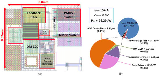
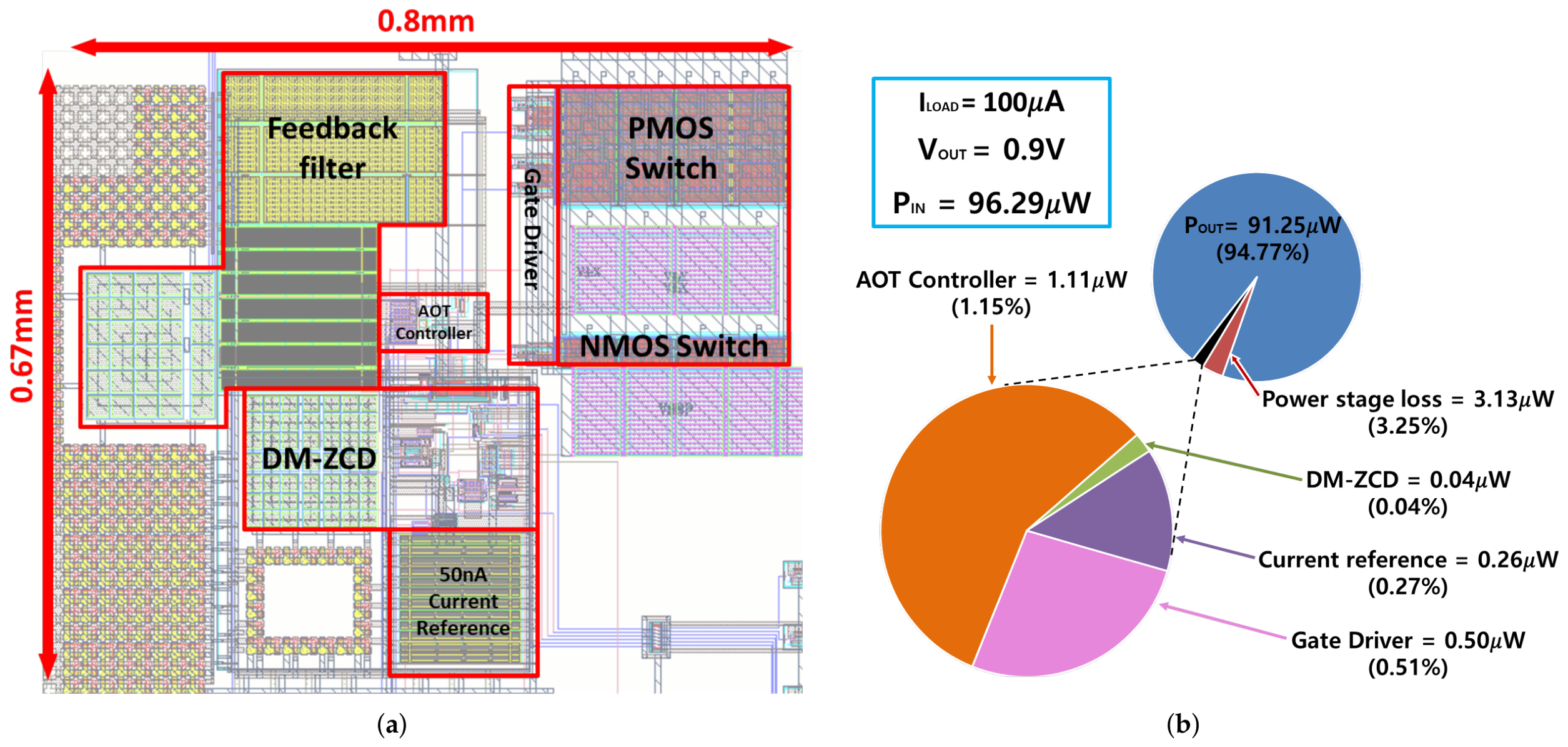
The proposed DC–DC buck converter employing the DM-ZCD, referred to as the DM-ZCD converter, was designed in a 0.18-μm CMOS process. Figure 17a shows the layout of the DM-ZCD converter, which occupies an active area of 0.34 mm2, while Figure 17b shows its power breakdown at V and μA. All post-layout simulation results were obtained using Cadence Virtuoso with the Spectre simulator. An off-chip 4.7 μH inductor with a DCR of 216 mΩ, an off-chip 4.7 μF output capacitor with an ESR of 6 mΩ and an ESL of 258 pH, and wire-bonding parasitics modeled as 50 mΩ/mm resistance and 1 nH/mm inductance were included in the simulations.
Figure 17.
(a) Chip layout and (b) power breakdown at V and μA.
Although the post-layout simulations include the modeled parasitic elements, additional losses may occur in actual silicon due to thermal effects, unmodeled PCB traces, and other non-idealities in the measurement environment. Therefore, the measured performance of the proposed converter may be slightly lower than the post-layout simulation results.
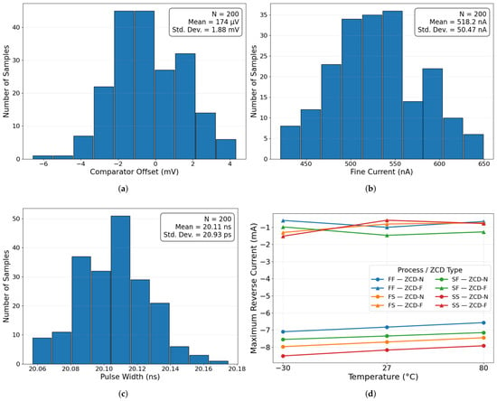
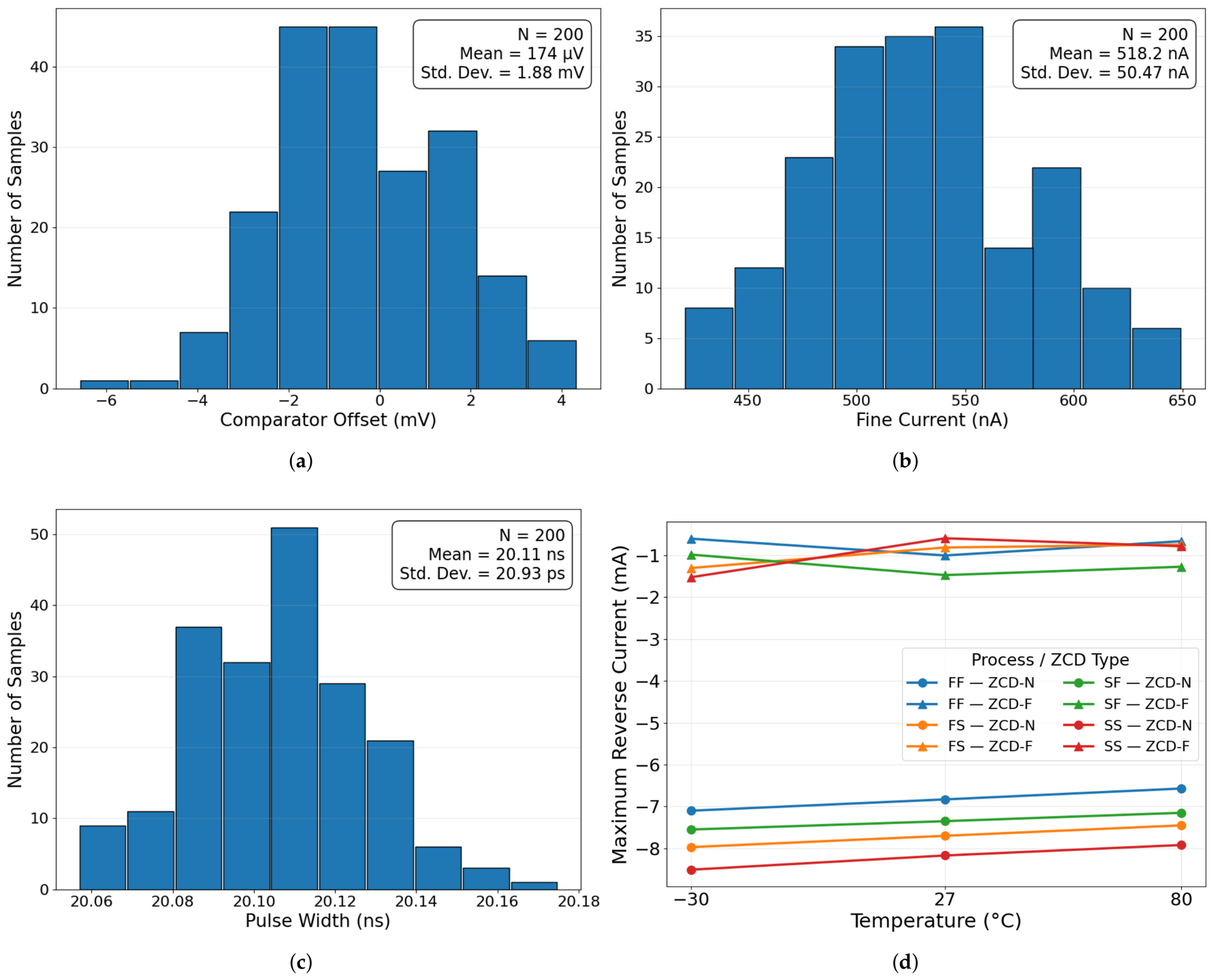
Since ZCD-N is inherently susceptible to non-ideal factors such as comparator offset and PVT variations, whereas ZCD-F is expected to be significantly less sensitive to these variations, their robustness is first evaluated. Figure 18a shows the statistical distribution of the ZCD-N comparator offset obtained from 200 Monte Carlo simulations. While the nominal ZCD-N operation results in an average reverse current of approximately 7 mA, the comparator offset can result in a reverse current of up to 41 mA or a forward current of up to 27 mA within the range. Therefore, when the ZCC detection error is quantified in terms of the reverse-current magnitude, the maximum error is increased by approximately 5.86 times compared with the nominal case.
Figure 18.
Monte Carlo and process temperature variation results: 200-run Monte Carlo simulations of (a) comparator offset, (b) fine current-source output, and (c) pulse width; (d) maximum reverse current of ZCD-N and ZCD-F under process and temperature variations.
In contrast, ZCD-F compares the voltage across , for which the is considerably larger than that of the used for ZCD-N; as such, it provides lower sensitivity to comparator offset. Nevertheless, according to (2), mismatch in the current-source output () and pulse width () can affect the tracking resolution of ZCD-F. The corresponding Monte Carlo simulation results are shown in Figure 18b and Figure 18c, respectively. Since the tracking resolution is determined by the product of these two parameters, the maximum tracking resolution within the range is approximately 1.2 times its nominal value. These results demonstrate that ZCD-F is significantly less sensitive to mismatch than ZCD-N.
As reported in [10], reverse current results in greater power loss than forward current, as it introduces not only diode conduction loss but also capacitor discharging loss. Moreover, the power loss caused by the reverse current is proportional to the cube of the ZCD timing error. Since the magnitude of the reverse current is linearly proportional to the ZCD timing error under the same operating condition, the increase in reverse current can be directly related to the increase in loss induced by the ZCD error. Accordingly, within the range, the maximum ZCD error-induced loss can increase by approximately 201 times for ZCD-N, whereas the corresponding increase for ZCD-F is limited to approximately 1.73 times.
The robustness of the two ZCD schemes against process and temperature variations is further evaluated in Figure 18d, which compares their maximum reverse-current magnitudes across the considered process corners and temperatures. Across these conditions, the maximum reverse-current magnitude varies over a range of 1.94 mA for ZCD-N, compared with only 0.92 mA for ZCD-F. These results further demonstrate that ZCD-F is considerably less sensitive to process and temperature variations than ZCD-N.
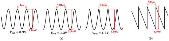
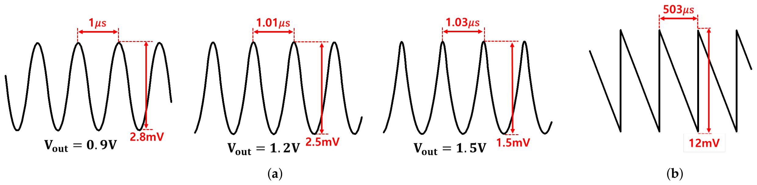
Figure 19 shows the switching period and the ripple under steady state for different operating conditions. As shown in Figure 19a, the switching period remains nearly constant even when varies in CCM ( mA). Figure 19b shows that the switching period increases significantly in DCM (μA) compared with that in CCM, implying a substantial reduction in switching loss. These results demonstrate the effectiveness of the proposed AOT-PFM control scheme.
Figure 19.
Switching period and ripple (a) at mA and (b) at V and μA.
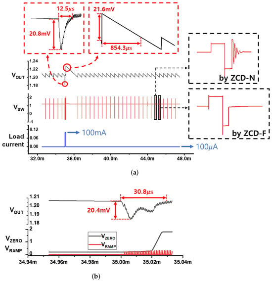
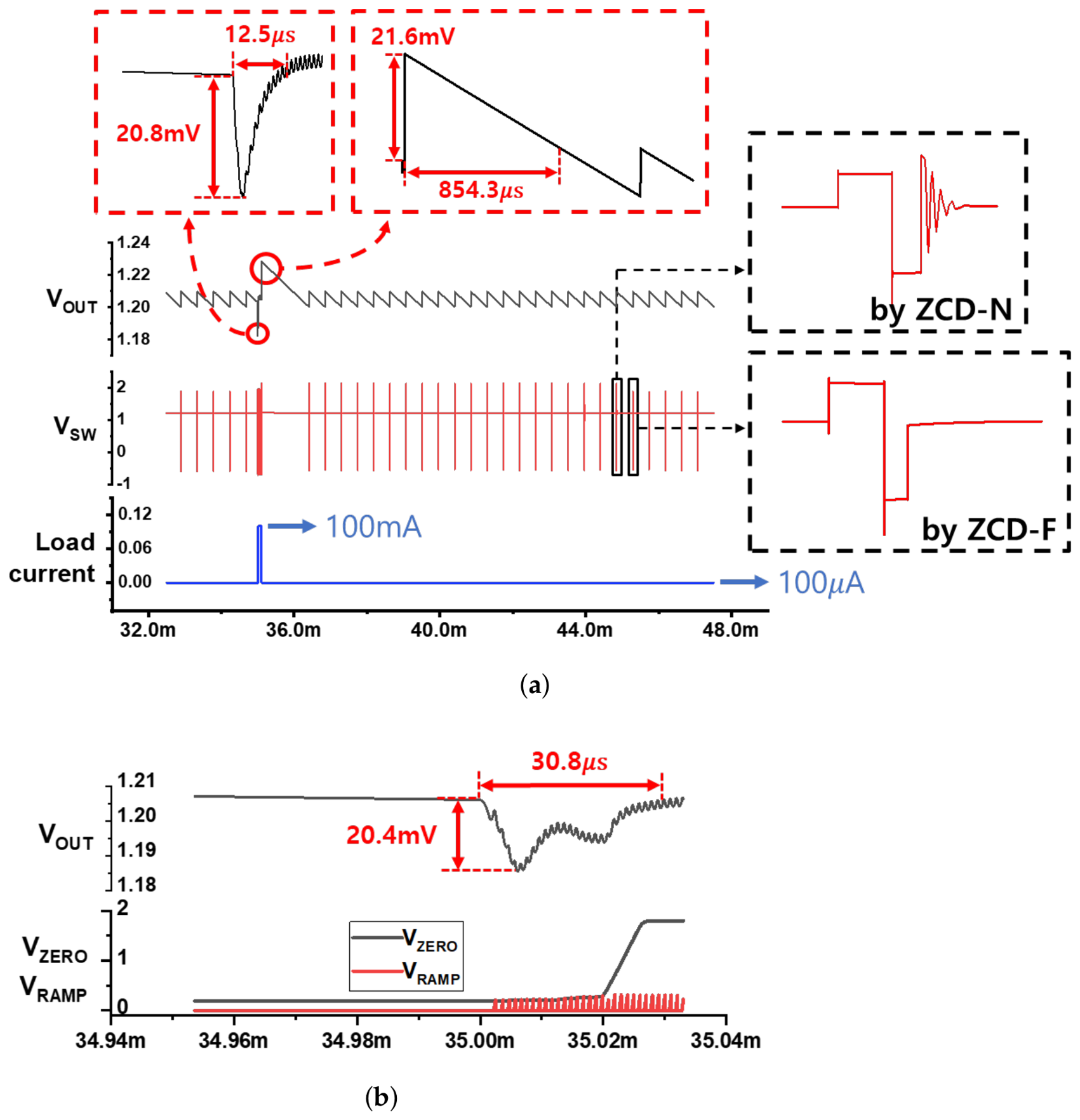
Figure 20a shows the waveforms of and during a load transition between 100 mA and 100 μA with a load-current transition time of 10 ns at V. Compared with the transient condition used in Section 3, this simulation employs a larger load step and a different output voltage. As observed from the waveform, the remains properly regulated even under this large load step. The waveform after the heavy-to-light load transition clearly shows the handoff of the ZCD scheme from ZCD-N to ZCD-F.
Figure 20.
Load transient waveforms between 100 mA and 100 μA at V with load-current transition times of (a) 10 ns and (b) 5 μs.
To further evaluate the handoff behavior under a slower load transition, Figure 20b shows the transient response under the same load step and output voltage conditions, but with the load-current transition time increased from 10 ns to 5 μs. Compared with the 10 ns case, the slower rise of increases the recovery time following the light-to-heavy load transition to approximately 30.8 μs. Nevertheless, is eventually properly regulated, while the response to the heavy-to-light load transition remains consistent with that observed in the 10 ns case. These results demonstrate that the proposed handoff mechanism maintains proper operation even under a significantly slower load transition.
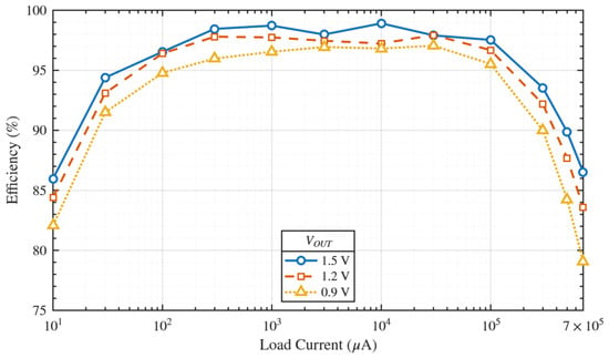
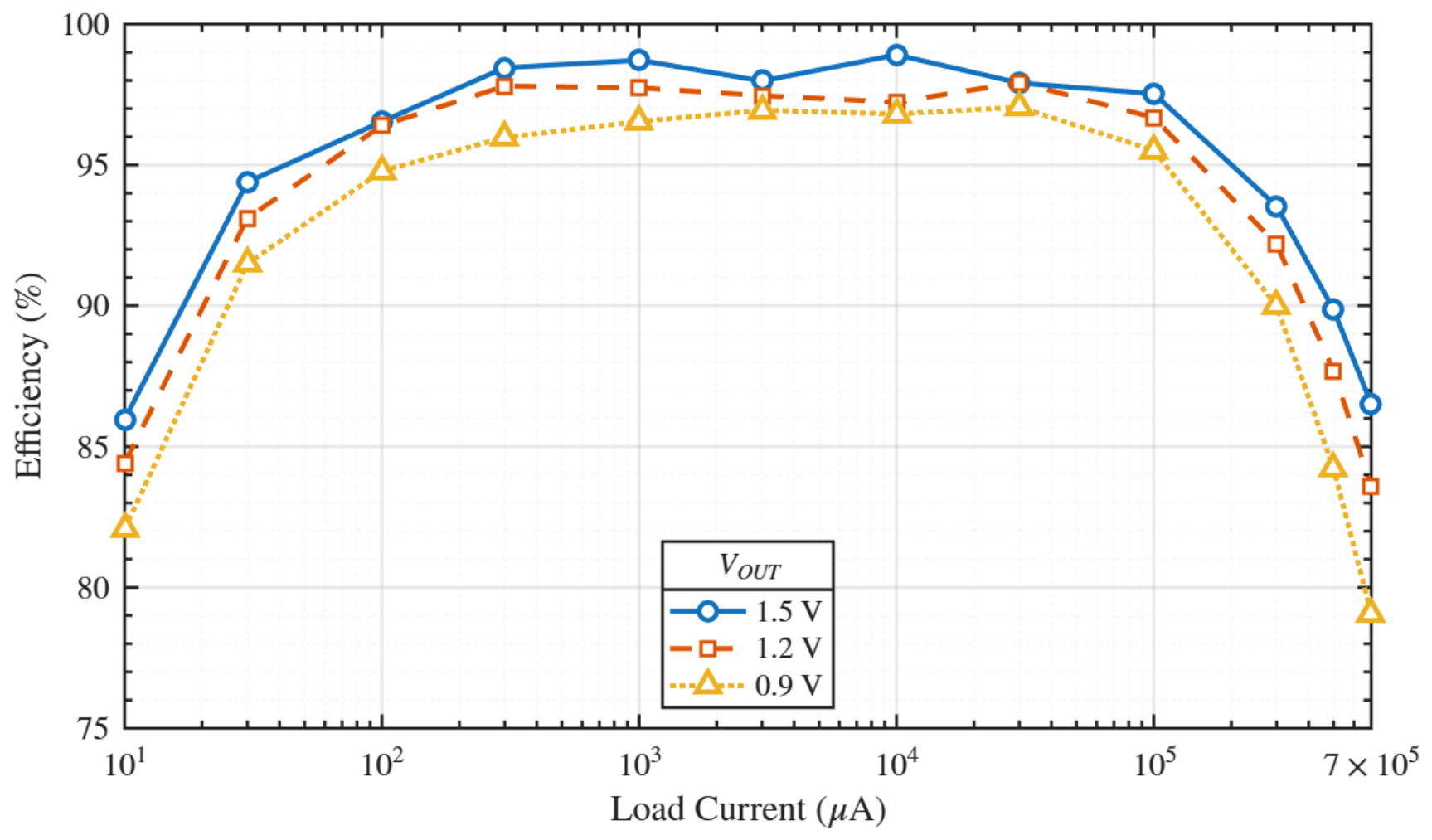
Figure 21 shows the simulated converter efficiency as and vary. The DM-ZCD converter achieves a peak efficiency of 98.9% at a voltage conversion ratio (VCR) of 0.83, corresponding to V and mA. The edge computing SoC application requires the converter to provide a sub-1 V output voltage. Under this operating condition, corresponding to V (), a peak efficiency of 97.1% is achieved while maintaining efficiency above 90% over a wide load range from 30 μA to 300 mA.
Figure 21.
Simulated converter efficiency versus .
To further quantify the individual contributions of the circuit-level techniques to the converter efficiency, additional ablation simulations were performed. First, the effect of dynamic biasing was evaluated by continuously maintaining the bias currents of all comparators at 2 μA. At V and μA, the conversion efficiency decreases from 96.40% with dynamic biasing to 92.18% under the fixed-bias condition, corresponding to a degradation of 4.22 percentage points. This result demonstrates that dynamic biasing plays an important role in maintaining high efficiency under light load conditions.
In addition, the contribution of the proposed subthreshold-biased comparator was evaluated by replacing the AOT comparator with a conventional comparator under the same bias condition. At V and mA, the conversion efficiency decreases from 97.38% to 96.39%, while the power consumption of the AOT controller increases from 2.052 μW to 29.862 μW. These results quantitatively demonstrate the contribution of the proposed comparator topology to reducing the control-circuit power consumption and improving the overall conversion efficiency.
Based on these simulation results, Table 4 compares the performance of the proposed DM-ZCD converter with that of previously reported buck converters employing DCM operation under light load conditions, including [16], which served as the basis for the proposed improvements. Since the results of the proposed converter are based on post-layout simulations, whereas all previous studies report physical measurement results, the actual measured efficiency of the proposed converter may be slightly lower than the reported simulation results.
Table 4.
Performance comparison of buck converters incorporating DCM operation for light load.
Among the compared converters in Table 4, the DM-ZCD converter achieves the second-widest load current range, with efficiency above 90%; this is surpassed only by JSSC’25 [5]. In addition, the DM-ZCD converter achieves the highest peak efficiency among all compared converters. These results demonstrate that the proposed design techniques, including the DM-ZCD scheme, dynamic biasing, and subthreshold-biased differential output stage, enable the converter to achieve state-of-the-art or near-state-of-the-art efficiency-related performance among converters incorporating DCM operation. Compared with [16], the chip area is increased, as both the ZCD scheme and the modulation method have been modified; however, a significant improvement in efficiency is achieved. In particular, the proposed DM-ZCD converter improves the peak efficiency by 4.9 percentage points compared with [16].
Table 5 shows the additional comparison of the performance between [16] and the DM-ZCD converter. To verify the effectiveness of the proposed design in preventing from turning on in CCM, the CCM efficiency should be compared. Although the load current corresponding to the peak efficiency of [16] is not specified, its efficiency curve indicates that the peak efficiency is achieved at approximately 100 mA in CCM. Therefore, the efficiency of the DM-ZCD converter was also simulated at and mA, resulting in a CCM efficiency of 96.7%, which corresponds to an improvement of 2.7 percentage points. These results quantitatively demonstrate the contribution of the proposed DM-ZCD scheme to the conversion efficiency by preventing from periodically turning on in CCM, unlike [16].
Table 5.
Comparison of ZCD and CCM performance between [16] and the DM-ZCD converter.
The zero-current self-tracking time is longer in the proposed converter due to the longer switching period resulting from the different modulation method. However, this drawback is mitigated by reducing the required number of cycles: ZCD-N captures the vicinity of ZCC and the mode decision circuit allows the ASTC operation to be influenced by ZCD-N, resulting in rapid discharge of during handoff. As a result, the proposed converter requires only 25 cycles for zero-current self-tracking, compared with 40 cycles in [16].
In addition, the DM-ZCD converter achieves significantly lower ZCD power. The reduced switching frequency at light loads reduces the activation frequency of the ZCD circuit, including the ASTC, while the use of a 50-nA current reference reduces the bias currents of the current sources in the ZCD circuit. Consequently, the ZCD power is reduced to 4.361 μW at 10 mA, compared with 81 μW in [16].
6. Conclusions
This paper presents an AOT buck converter with a DM-ZCD scheme for high-efficiency operation over a wide load range in edge computing SoC applications. ZCD-N determines whether a transition to DCM is required without periodically activating the during CCM, and rapidly detects the vicinity of the ZCC during the initial CCM-to-DCM transition. The ZCD scheme is then transferred to ZCD-F for accurate ZCC tracking and suppression of switching-node LC oscillations in steady-state DCM. During DCM-to-CCM transition, the absence of a ZCD-F event automatically re-enables the ZCD-N circuit. The AOT controller provides near-constant frequency operation in CCM and load-dependent frequency operation in DCM, reducing switching loss in DCM. Dynamic biasing and a subthreshold-biased differential stage in the AOT comparator reduce control-circuit power consumption and short-circuit current in the comparator output buffer, respectively, while maintaining reliable operation.
Designed in a 0.18-μm CMOS process, the DM-ZCD converter operates from a 1.8 V input with an output voltage range of 0.8-1.5 V and a load current range of 10 μA to 700 mA. Post-layout simulation results predict a peak efficiency of 98.9% at V and mA. At V, the converter achieves a peak efficiency of 97.1% and maintains an efficiency above 90% over a load range from 30 μA to 300 mA. The proposed event-based handoff between ZCD schemes enables efficient operation over a wide load range.
Author Contributions
Conceptualization, methodology, and validation: S.-Y.L.; investigation, resources, and data curation: S.-Y.L. and D.-H.S.; writing—original draft preparation: S.-Y.L.; writing—review and editing: D.-H.S. and K.-H.B.; supervision and project administration: K.-H.B. All authors have read and agreed to the published version of the manuscript.
Funding
This research was supported by the Chung-Ang University Graduate Research Scholarship in 2025, in part by a National Research Foundation of Korea (NRF) grant funded by the Korean government (MSIT) in 2026 (Grant No. RS-2026-25591915, Project Title: Development of Highly Reliable Multi-Standard Automotive SerDes IP for SDVs in Harsh Automotive Environments), and in part by the National R&D Program through the National Research Foundation of Korea (NRF), funded by the Ministry of Science and ICT (RS-2021-NR057239).
Data Availability Statement
The data presented in this study are available upon request from the corresponding author. The data are not publicly available due to privacy.
Conflicts of Interest
The authors declare no conflicts of interest.
Abbreviations
The following abbreviations are used in this manuscript:
| PULP | Parallel Ultra-Low-Power |
| AOT | Adaptive On-Time |
| DCM | Discontinuous Conduction Mode |
| CCM | Continuous Conduction Mode |
| VCR | Voltage Conversion Ratio |
| ZCD | Zero-Current Detection |
| ZCD-N | NMOS switch-based ZCD |
| ZCD-F | Freewheeling switch-based ZCD |
| DM-ZCD | Dual-Mode ZCD |
| ZCC | Zero-Current Crossing |
| DFF | D Flip-Flop |
| ASTC | Analog Self-Tracking Circuit |
| CEG | Coarse_en Generator |
References
- Bonomi, F.; Milito, R.; Zhu, J.; Addepalli, S. Fog Computing and Its Role in the Internet of Things. In Proceedings of the 1st Workshop on Mobile Cloud Computing (MCC), New York, NY, USA, 17 August 2012; pp. 13–16. [Google Scholar]
- Pullini, A.; Rossi, D.; Loi, I.; Tagliavini, G.; Benini, L. Mr.Wolf: An Energy-Precision Scalable Parallel Ultra Low Power SoC for IoT Edge Processing. IEEE J. Solid-State Circuits 2019, 54, 1970–1981. [Google Scholar] [CrossRef] [Scilit]
- Flamand, E.; Rossi, D.; Conti, F.; Loi, I.; Pullini, A.; Rotenberg, F.; Benini, L. GAP-8: A RISC-V SoC for AI at the Edge of the IoT. In Proceedings of the 2018 IEEE 29th International Conference on Application-Specific Systems, Architectures and Processors (ASAP), Milan, Italy, 10–12 July 2018; pp. 1–4. [Google Scholar]
- Conti, F.; Schilling, R.; Schiavone, P.D.; Pullini, A.; Rossi, D.; Gürkaynak, F.K.; Muehlberghuber, M.; Gautschi, M.; Loi, I.; Haugou, G.; et al. An IoT Endpoint System-on-Chip for Secure and Energy-Efficient Near-Sensor Analytics. IEEE Trans. Circuits Syst. I Regul. Pap. 2017, 64, 2481–2494. [Google Scholar] [CrossRef] [Scilit]
- Wang, B.; Xie, Y.; Cheng, L.; Guo, J. A Single Li-Ion Battery Powered Buck Converter with >90% Efficiency Over 10-μA to 500-mA Loading Range by Utilizing Compensator-Based Built-In Mode Tracking Technology. IEEE J. Solid-State Circuits 2025, 60, 1743–1755. [Google Scholar] [CrossRef] [Scilit]
- Huang, W.; Liu, L.; Liao, X.; Xu, C.; Li, Y. A 240-nA Quiescent Current, 95.8% Efficiency AOT-Controlled Buck Converter with A2-Comparator and Sleep-Time Detector for IoT Application. IEEE Trans. Power Electron. 2021, 36, 12898–12909. [Google Scholar] [CrossRef] [Scilit]
- Zhao, M.; Li, M.; Song, S.; Hu, Y.; Yao, Y.; Bai, X.; Hu, R.; Wu, X.; Tan, Z. An Ultra-Low Quiescent Current Tri-Mode DC-DC Buck Converter with 92.1% Peak Efficiency for IoT Applications. IEEE Trans. Circuits Syst. I Regul. Pap. 2022, 69, 428–439. [Google Scholar] [CrossRef] [Scilit]
- Zeng, W.L.; Ren, Y.; Lam, C.S.; Sin, S.W.; Che, W.K.; Ding, R.; Martins, R.P. A 470-nA Quiescent Current and 92.7%/94.7% Efficiency DCT/PWM Control Buck Converter with Seamless Mode Selection for IoT Application. IEEE Trans. Circuits Syst. I Regul. Pap. 2020, 67, 4085–4098. [Google Scholar] [CrossRef] [Scilit]
- Cao, P.; Wang, Y.; Xu, J.; Hong, Z. A 55nA Quiescent Current Power-Wise Buck Converter with 1μA–600mA Load Range and 0.5V–1.8V Flexible Output Voltage Options. IEEE Trans. Circuits Syst. I Regul. Pap. 2025, 72, 397–407. [Google Scholar] [CrossRef] [Scilit]
- Liu, Z.; Goh, W.L.; Siek, L.; Gao, Y. A 310 nA DCM Hysteretic Buck Converter with 95.8% Peak Efficiency and Greater Than 90% Efficiency in 10 μA–100 mA Load Range for Battery Powered IoT Sensors. IEEE Trans. Circuits Syst. I Regul. Pap. 2025, 72, 6691–6700. [Google Scholar] [CrossRef] [Scilit]
- Shi, Y.; Liu, X.; Li, X.; Wang, S.; Peng, L.; Zhou, Z.; Zhang, B. An Ultra-Low Quiescent Current Adaptive ZCD Technique for Discontinuous-Conduction-Mode Control Applications. IEEE Trans. Circuits Syst. II Express Briefs 2025, 72, 1635–1639. [Google Scholar] [CrossRef] [Scilit]
- Kim, S.-Y.; Park, Y.J.; Ali, I.; Nga, T.T.K.; Ryu, H.C.; Khan, Z.H.N.; Park, S.M.; Pu, Y.G.; Lee, M.; Hwang, K.C.; et al. Design of a High Efficiency DC-DC Buck Converter with Two-Step Digital PWM and Low Power Self-Tracking Zero Current Detector for IoT Applications. IEEE Trans. Power Electron. 2018, 33, 1428–1439. [Google Scholar] [CrossRef] [Scilit]
- Meng, X.; Sun, K.; Xi, J.; He, L. Real Time Zero Current Detection with Low Quiescent Current for Synchronous DC-DC Converter. In Proceedings of the 2017 IEEE 26th International Symposium on Industrial Electronics (ISIE), Edinburgh, UK, 19–21 June 2017; pp. 839–843. [Google Scholar]
- Hsu, Z.-Y.; Liu, C.-W.; Wu, J.-W.; Chang, W.-J.; Li, T.-L.; Chen, P.-H. A Single-Inductor Triple-Output Buck-Boost Converter with Output Ripple Control for Wearable Devices. In Proceedings of the 2022 IEEE International Symposium on Circuits and Systems (ISCAS), Austin, TX, USA, 27 May–1 June 2022; pp. 3575–3578. [Google Scholar]
- Chen, P.-H.; Wu, C.-S.; Lin, K.-C. A 50 nW-to-10 mW Output Power Tri-Mode Digital Buck Converter with Self-Tracking Zero Current Detection for Photovoltaic Energy Harvesting. IEEE J. Solid-State Circuits 2016, 51, 523–532. [Google Scholar] [CrossRef] [Scilit]
- Woo, K.-C.; Oh, J.-M.; Yang, B.-D. DC-DC Buck Converter Using Analog Coarse-Fine Self-Tracking Zero-Current Detection Scheme. IEEE Trans. Circuits Syst. II Express Briefs 2019, 66, 1850–1854. [Google Scholar] [CrossRef] [Scilit]
- Razavi, B. The StrongARM Latch [A Circuit for All Seasons]. IEEE Solid-State Circuits Mag. 2015, 7, 12–17. [Google Scholar] [CrossRef] [Scilit]

Disclaimer/Publisher’s Note: The statements, opinions and data contained in all publications are solely those of the individual author(s) and contributor(s) and not of MDPI and/or the editor(s). MDPI and/or the editor(s) disclaim responsibility for any injury to people or property resulting from any ideas, methods, instructions or products referred to in the content. |
© 2026 by the authors. Licensee MDPI, Basel, Switzerland. This article is an open access article distributed under the terms and conditions of the Creative Commons Attribution (CC BY) license.