


Abstract
Computing in memory represented by resistive switching (memristive) devices is a promising way to implement hardware for artificial neural networks. We see it as the way to create energy-efficient and high-performance systems for solving a wide range of tasks in artificial intelligence. Here, we present the structure and performance of our crossbar array based on Au/Ta/ZrO2(Y)/Pt/Ti memristive devices, integrated into a complementary metal–oxide–semiconductor fabrication process, and then demonstrate its applicability for the hardware implementation of artificial neural networks. The array contains 256 memristive devices combined into 32 columns and eight rows. Each memristive device is paired with an n-channel metal–oxide–semiconductor transistor. As the results of the simulations show, these devices enable running neural network algorithms for solving recognition problems using the Modified National Institute of Standards and Technology dataset with 98% accuracy and the Canadian Institute for Advanced Research (10 classes) dataset with at least 77.5% accuracy, even taking into account the errors of mapping weights onto the memristive crossbar. Fully hardware recognition of 4 bit images demonstrated in this work highlights the crucial role of selective transistors for such tasks. This paper explores the exciting potential of memristor-based components of neuroelectronics as the building blocks for a new era of artificial intelligence hardware, capable of surpassing current computational limitations, as well as their role in the ongoing transition to hybrid intelligence based on the symbiosis of electronic and biological systems.
1. Introduction
A memristor is a passive element of electronics that changes its resistance due to the history of the electric current, and is capable of maintaining an altered resistive state for a long time [1], by which we mean even for years [2]. This resistance change is achieved through resistive switching, which can originate from various physical mechanisms, including, among others, electrochemical metallization, valence changes, thermochemical processes, phase transitions, ferroelectric or ferromagnetic domain polarization, electrostatic and electronic effects, as well as nanomechanical and molecular effects [3]. Of the above, filamentary switching, where the resistance change is governed by the restoration and rupture of localized conductive paths (filaments), which has been confirmed by direct experimental observations [4,5], is widespread and serves as the basis for several distinct mechanisms. In particular, two redox-based filamentary mechanisms are most commonly discussed: valence change mechanism [6,7], governed by the migration of oxygen vacancies, and electrochemical metallization [8,9], where the filament is formed by metal cations (e.g., Cu or Ag). A third one, the thermochemical mechanism, which involves a thermally induced change in stoichiometry, has also been described in the literature [10,11], although it is less frequently addressed in recent studies. In addition to filamentary switching, non-filamentary mechanisms have been observed, including interfacial switching [12,13], in which the resistance change is controlled by the modulation of the carrier transport barrier at the electrode/switching layer interface, and bulk-type switching [14,15], which occurs throughout the volume of the switching layer. Regardless of the specific mechanism, memristive devices offer unique advantages for computing applications.
It was indicated by the simulation results [16], as well as the hardware implementation of memristor-based computing systems, that they can reduce power consumption and increase the efficiency of inference and training of artificial neural networks (ANNs) by several orders of magnitude compared to graphics processing units (GPUs) and tensor processing units (TPUs) [17,18]. This advantage is achieved due to two key principles–the use of a chip architecture different from von Neumann’s, in which calculations are performed distributed in many cores that store synapse values and work as neurons [19], and the calculation of matrix multiplication in analog mode due to Ohm’s and Kirchhoff’s laws in crossbar arrays of memristive devices [20,21], where the energy is spent only on the resistive state switch, but not to maintain the weights, as is done in back-propagation algorithms [22] widely used in traditional ANNs. The main advantage of the proposed hardware system over conventional digital systems lies in performing computations directly in memory [23]. This avoids the energy-intensive and slow data transfer between the memory and the processing unit that is inherent to the von Neumann architecture [24]. In a memristive crossbar, the vector-matrix multiplication that dominates neural network workloads is carried out in a single step by Ohm’s and Kirchhoff’s laws, whereas a digital processor requires a large number of sequential operations for the same task.
These principles provide an option to create computing systems that require orders of magnitude fewer memory access operations without repeatedly transferring data from cache to cache (namely, in-memory computing) while performing fewer calculations by eliminating the excessive accuracy of weights and data for neural networks [25]. Further, such systems are characterized by the sparsity of calculations, since they are performed only for those neurons that are currently active, which allows for stable latency when processing data streams. In addition, memristor synapses have the plasticity inherent in living synapses [26,27,28], which provides an option for creating neuromorphic chips with local learning [29,30,31,32], as well as hardware for implementing various biologically plausible principles of information processing in the nervous system, such as astrocytic regulation [33] and synchronization [34], and even for implementing a biologically plausible part of the spinal cord [35]. Beyond bio-inspired systems, memristors have also been investigated for digital logic [36,37,38] and in-memory computing circuits. Various experimental studies have shown that memristors can recognize images [39,40,41,42], sounds [43,44,45] and other patterns [46,47,48] with high accuracy after training, indicating promising potential for practical applications of memristors in areas such as robotics, autonomous systems and neuroprosthetics, as well as in other real-time signal processing devices [49,50,51,52,53,54,55]. Recent reviews have systematically addressed the key parameters and optimization strategies for such neuromorphic systems [56,57,58,59,60]. Beyond conventional neuromorphic computing, emerging memristive devices with stimulus-responsive dynamics are opening new opportunities for in-sensor computing, that is, the integration of sensing, memory, and computation functionalities [61], as recently shown in a broader class of artificial sensory systems that emulate vision, touch, olfaction, audition and gestation [62,63,64,65,66]. This trend is exemplified by humidity-driven in-sensor platforms [67] and in systems capable of detecting pain [68].
We consider that the critical task of creating the memristive neuromorphic processor is the creation and comprehensive optimization of crossbar arrays of memristive devices, which could play the role of resistive random-access memory cells, providing an option to implement the calculations in memory. The architecture based on memristive crossbar arrays, as already shown in recent studies, can be effectively used to solve linear algebra problems such as linear equations, matrix multiplication, matrix eigenvectors, matrix inversion, differential equations and so on [69,70,71,72,73], as well as non-linear equations such as the Riccati matrix equation [74], the non-linear partial differential equation [75,76] or other complex applications, such as real-time image recognition and image enhancement [77,78]. Thus, the presented architecture is not only functionally demonstrative but also theoretically justified as an efficient substrate for analog matrix operations.
Currently, both very large memristor crossbar arrays containing tens and hundreds of thousands of elements (256 × 256 [79], 500 × 661 [80], 2048 × 512 [81]) and small ones containing hundreds and thousands of devices (12 × 12 [82], 16 × 16 [83], 64 × 64 [84]) have been developed. The question of the optimal size of the crossbar array remains open at the moment, since there are successful examples of using both small 256-element crossbar arrays in NeuRRAM [85] and arrays of 65,536 memristors in TetraMEM [86] as part of neuromorphic processor prototypes. In both cases, despite the different numbers of cells in the crossbar array, their total number increases to millions due to the use of scalable distributed architectures. We consider that it is critical for future technology to provide the crossbar arrays with high cell density, low resistance variations and high switching reliability.
In this paper, we describe our development of a 32 × 8 1T1R memristive crossbar array based on a ZrO2(Y) switching layer, which operates via the valence change mechanism [87]. These solutions include the layout of the test crystal and the manufacturing process for memristive devices onto a device layer containing transistors as control selector elements, fabricated within the framework of a 350 nm complementary metal–oxide–semiconductor (CMOS) fabrication process using silicon-on-insulator (SOI) technology. The results of the sample fabrication were analyzed in detail using transmission electron microscopy (TEM). We also show the results of characterization of the created devices, demonstrating I–V curves, retention, endurance and synaptic plasticity. Finally, we demonstrate the operation of a simple hardware neural network for the binary classification of signal patterns and also extend the experimental data to a large neural network for classifying images from the Canadian Institute for Advanced Research 10-class (CIFAR-10) dataset.
While the conceptual framework of using memristive crossbar arrays for in-memory computing and neuromorphic applications is not entirely new, the novelty of the present work lies not in the simple creation of yet another memristive crossbar array, but in the comprehensive demonstration of the complete development cycle—from materials science to system-level simulation and hardware-validated neuromorphic applications. In contrast to studies that focus either on individual devices or on simulations alone, this study demonstrates the successful integration of a well-proven laboratory-tested memristive structure based on ZrO2(Y) into a standard CMOS fabrication process. While 1T1R crossbar arrays have been reported using various material systems, the specific combination of a ZrO2(Y)-based memristive stack with 1T1R CMOS integration, 16-level multistate retention, long-term stability of these states (retention > 104 s for extreme states and >300 s for 16 states), endurance exceeding 107 cycles and experimental hardware classification in a single fabricated chip has not been demonstrated previously, advancing the practical feasibility of such systems for neuromorphic applications.
2. Materials and Methods
2.1. Crossbar Architecture and Device Fabrication
The crossbar array is a matrix of 32 × 8 1T1R cells (Figure 1a). Each element of the matrix (cell) consists of a series-connected memristor and a selector on an n-channel field-effect transistor (Figure 1b), a configuration known in the literature as one of the most high-density designs [88]. The transistor gates are combined into eight control WordLines (WL0…WL7), and the substrates are connected together. The columns of the crossbar array are connected to the bottom electrode (BE) of the memristive device (BitLines, BL0…BL31), and the rows represent the top electrodes (TE) (NetLines, Net0…Net7). WordLines allow one to control access to cells both by individual columns and to all cells at once. The threshold voltage of the n-channel metal–oxide–semiconductor (NMOS) transistors is +3.3 V, and the driver current is selected in such a way that it exceeds the values of the maximum operating currents through the memristor.
Figure 1.
The developed crossbar array of memristive devices. (a) The layout of a crossbar array consisting of 32 × 8 memristive devices. (b) A circuit diagram of a single cell. (c) Schematic representation of the structure of one cell of the crossbar array. (d) A photo of the chip in the case and an enlarged photo of the crossbar array obtained by optical microscopy.
Such a cell has several features related to its asymmetry. Depending on the polarity of the applied voltage, if the switching direction is important, one of the processes will implement a circuit for switching on the source repeater, limiting the voltage drop across the memristor to VGS − VTH. The resistance range of the memristive device plays a huge role in this case, since it will directly affect the current flowing through the cell during switching, as well as the operating mode of the transistor. Memristive devices with large resistances (more than 10 kΩ) are preferred in 1Т1R-type cells, since this makes it possible to set the required operating mode of the transistor with its smaller size. In the opposite process, the transistor operates in switch mode; the voltage drop across it is minimal and is determined solely by its size and channel length. This limitation can be avoided by adding a complementary p-channel current-switching device that ensures operation in switch mode with the desired switching polarity.
The chip was fabricated in two stages. As part of the front-end-of-line (FEOL) process, a device layer containing n-channel transistors is fabricated under industrial conditions with design standards of 350 nm for the CMOS fabrication process using SOI technology. The layout provides for super-dense filling to level the surface of the device layer and contains an additional layer of SiO2 with windows above the BE to protect the peripheral areas of the memristive devices from leaks and breakdowns. Then, within the framework of the back-end-of-line (BEOL) process, the integration of the memristive structure onto the 4th level of metallization is performed. For this purpose, a constructive version of the “metal-oxide-metal” memristive structure (Figure 1c) based on yttria-stabilized zirconia (ZrO2(Y)) is used as a basis. It is a transition metal oxide with a predominant ionic chemical bond, known as an ionic electrolyte, in which a dopant, yttrium oxide, with a concentration of 12 mol. % stabilizes the cubic phase of ZrO2 and sets a certain concentration of oxygen vacancies, which play a crucial role in resistive switching—the formation and local destruction/restoration of conductive filaments in the oxide film [89,90,91]. The memristive structures were formed by magnetron sputtering under the following conditions. The bottom Pt electrode (40 nm thick) with adhesive Ti sublayer (10 nm thick) was deposited at a substrate temperature of 200 °C. The ZrO2(Y) film (20 nm thick) was deposited using a pressed powder target from a mixture of ZrO2 and dopant Y2O3 (12 mol. %) at a substrate temperature of 300 °C. A top Au electrode (40 nm thick) with a Ta sublayer (40 nm thick) was deposited at a substrate temperature of 200 °C. The active area was 10 × 10 μm2.
Figure 1d shows a photo of the finished chip. The area occupied by a crossbar array on a crystal is 25 mm2. The crystal is mounted in a 5134.64-6 metal-ceramic case for research. All applied technological processes relate to the standard operations used for the fabrication of analog–digital chips.
For the thermal stability study, individual memristors with an area of 10−3 cm2 were used. The devices had the same composition and thickness as those in the 32 × 8 crossbar array but were fabricated on a common bottom electrode, ensuring representativeness of the results.
2.2. Characterization of the Memristive Device
Electrophysical characterization of the memristive devices was carried out using the National Instruments USB-6361 multifunction data acquisition device (Austin, TX, USA), programmable in LabVIEW v. 19.0. In these experiments, the sign of the voltage across the memristive device corresponded to the potential of the Pt electrode relative to the potential of the Au electrode.
The 150 I–V curves of the device were measured by applying a voltage sweep. The average I–V curve was calculated using all the measured curves.
The stability of extreme resistive states as a function of the retention time was studied. For this purpose, the memristive device was first switched to high resistance state (HRS) or low resistance state (LRS) by applying a voltage pulse with an amplitude of +1.2 V or −0.9 V, then this state was read for 10,000 s every second by applying a reading pulse with an amplitude of +0.3 V at room temperature.
The endurance of the extreme resistive states was also studied. The data were obtained using pulses with the following parameters: the duration of all pulses was 12 μs; the amplitude of the pulses used to switch to the HRS (RESET pulse) was +1.15 V, to the LRS (SET pulse) −1 V; the amplitude of the reading pulses was +0.3 V.
To study potentiation/depression, a signal consisting of a single RESET pulse/SET pulse with an amplitude of +1.2 V/−0.9 V and a duration of 20 μs and a series of 100 potentiation/depression pulses with an amplitude of −0.75 V/+1.05 V and a duration of 2 μs was applied to the memristive devices. After each pulse, the current through the device was measured by applying reading pulses with an amplitude of +0.3 V and a duration of 15 μs. In total, 100 cycles of RESET potentiation and 100 cycles of SET depression were measured.
The thermal stability of the memristive devices was assessed by measuring their endurance over a wide temperature range from −146 °C to +250 °C. The measurements were performed using an Agilent B1500A semiconductor parameter analyzer (Santa Rosa, CA, USA). Current compliance was −300 μA and is based on a simple field-effect transistor circuit. During the measurements, the sample was placed inside a sealed metal thermostat in an atmosphere dried with silica gel. Cooling and heating were achieved by putting the thermostat in liquid nitrogen or placing it on a hot plate, respectively. The temperature was monitored with a Fluke 17B+ digital multimeter (Everett, WA, USA). The measurements were carried out as follows. At each temperature, 100 consecutive I–V curves were recorded. The endurance data were obtained by extracting the current at 0.3 V from each consecutive I–V curve.
Experiments on programming and retention of 16 resistive states were performed using the National Instruments PXIe-4140 source measure unit (Austin, TX, USA), programmable in LabVIEW v. 15.0. The programming of 16 different resistive states was performed by an algorithm based on the supply of voltage pulses with varying amplitude, which did not exceed ±4 V, and duration, varying randomly in a given range (10–100 ms), followed by reading the resistive state at each step [92]. The amplitude of the reading pulses was +0.1 V, and the duration was 10 ms. The retention of each of the programmed resistive states was also investigated for 300 s by applying reading pulses every second with the same amplitude and duration.
The study of the memristor cross-section in an integrated circuit was carried out using the JEOL JEM-2100F transmission electron microscope (Akishima, Tokyo, Japan) with an accelerating voltage of 200 kV, equipped with an Oxford Instruments X-Max energy dispersive X-ray detector (Abingdon, Oxfordshire, UK). The cross-section was made using an upgraded preparation technology based on the technology described in [93].
2.3. Neural Network Simulation
The simulations were performed using Python v. 3.12.10 and the PyTorch library v. 2.13.0. The network for CIFAR-10 was simulated using the Google Colab service. Images from the CIFAR-10 dataset were upscaled from their original 32 × 32 resolution to 224 × 224 pixels. The original Modified National Institute of Standards and Technology (MNIST) and CIFAR-10 training datasets were randomly divided into training and validation subsets at an 80:20 ratio. The final results were obtained on test datasets. The datasets were subdivided into mini-batches of size 256. Both datasets were normalized conventionally. The network architecture comprised 2 fully connected layers (784 × 512 × 10) for MNIST. For CIFAR-10, a ResNet-18 model, pre-trained on ImageNet with frozen weights, was modified by replacing the final layer with a trainable 512 × 10 layer. The network architectures are presented in Figure 2a,b.
Figure 2.
The network architectures. (a) Classification using the Modified National Institute of Standards and Technology (MNIST) dataset with a 2-layer fully connected network. (b) Classification using the Canadian Institute for Advanced Research 10-class (CIFAR-10) dataset with a pre-trained ResNet-18 network with fixed weights and a trainable fully connected output layer.
The weights of the trainable layers were initialized from a normal distribution with 0 mean and 0.01 standard deviation before the training process. For simplicity, biases were omitted from the trainable network parts. The cross-entropy loss function and Adam optimizer with standard parameters were used to train both networks. The MNIST network employed rectified linear unit (ReLU) activation, whereas the CIFAR-10 trainable layer used no activation function. The network weights were adjusted using the error back-propagation algorithm after processing each mini-batch. The network was trained for 100 epochs for MNIST and 10 epochs for CIFAR-10. Then, the memristive characteristics (Figure 3a) were introduced as follows [94,95]. The measured resistances of the 16 stable states were converted to conductances and multiplied by a scaling factor of 111. This factor was introduced to bring the memristive weights into the same range as the software ones. A single synaptic weight was encoded by a pair of memristors and taken as the difference of their scaled conductances, w = G+ − G−. Since each conductance is non-negative, the differential pair covers both positive and negative weights. After the network had been trained in full precision, every weight was replaced by the closest value from the set of all available differences of the 16 states. Next, the memristive stochasticity was introduced. The states in Figure 3a do not hold their resistances perfectly over time due to the inherent stochasticity of resistive switching [96,97,98]. Therefore, each G was sampled independently from a normal distribution centered at the mean conductance of the corresponding state, with the standard deviation set by the experimental coefficient of variation (or a larger one to simulate device degradation). This procedure corresponds to the simulation of the off-chip training with introduced memristive discretization and stochasticity of the weights. In the case of on-chip training simulation, the same discretization and sampling procedure was applied at each training step of the network. Each memristive simulation was repeated 10 times to obtain statistics.
Figure 3.
Typical characteristics of ZrO2(Y)-based memristive devices in a crossbar array. (a) Multilevel retention of the resistive states (4 bits). (b) The 150 I–V curves (the average I–V curve is indicated in orange). (c) Endurance of extreme resistive states.
3. Results and Discussion
3.1. Electrophysical Characterization
According to the results of the experimental studies, the fabricated memristive devices demonstrate reproducible bipolar resistive switching in both continuous and pulsed modes at voltages in the range ±(0.5–1.2) V (Figure 3b). The SET process, the transition from an HRS to an LRS, corresponds to the restoration of filaments in the oxide layer, and the RESET process, the transition from an LRS to an HRS, is associated with the oxidation of filaments near the interface with the active electrode.
The devices exhibit at least 16 clearly distinguishable and time-stable resistive states (Figure 3a, Table S3). The results of a study of the retention of the extreme resistive states (HRS and LRS) of a memristive device at room temperature show that over 10,000 s, the extreme resistive states do not overlap and have a small scatter, which indicates the excellent properties of the device’s non-volatility (Figure S2).
The device demonstrated more than 107 cycles of resistive switching in pulse mode without significant degradation (Figure 3c). The results of the statistical analysis of these data also indicate a high stability of resistive states (µ is the average value, σ is the standard deviation, and c is the coefficient of variation): μHRS = 0.07 mA, σHRS = 0.02 mA, cHRS = 28.6%; μLRS = 0.58 mA, σLRS = 0.01 mA, cLRS = 1.7%. Furthermore, independent experiments on comparable devices with the same ZrO2(Y)-based memristive stack have demonstrated failure-free operation up to 1010 switching cycles [99].
Important properties of memristive devices in the hardware implementation of ANNs include the characteristics of synaptic plasticity (dynamic range, degree of nonlinearity, and conductivity fluctuations) [100], which describe changes in the value of the current flowing through the memristive device at the reading voltage due to the action of a series of pulses. This behavior is similar to the processes of potentiation and depression—the ability of a synapse to change the strength of the connection between neurons [101].
Typical results of the study of potentiation and depression are presented in Figure 4 and Figure S2. It can be seen that there is no significant degradation of synaptic plasticity characteristics during multiple cycles of potentiation/depression. The absence of overlap in the calculated values of the change in synaptic weight and the small variation indicate the potential for using the developed memristive devices as electronic neurons and synapses.
Figure 4.
Typical synaptic plasticity of ZrO2(Y)-based memristive devices: (a) potentiation and (b) depression. Each figure shows 40 cycles.
Although the devices demonstrate stable potentiation and depression over multiple cycles, the nonlinear synaptic potentiation and depression behaviors are common features of memristors and may affect the accuracy of synaptic weight tuning [102]. Several strategies have been proposed to improve the linearity of synaptic weight modulation. At the programming level, pulse engineering techniques, such as gradually increasing the amplitude or duration of consecutive pulses, have been shown to improve the linearity of conductance modulation [103,104,105]. At the device level, the use of a 1T1R configuration with a series transistor has been demonstrated to enable linear and symmetric conductance tuning by controlling the compliance current during programming [106,107]. From a materials engineering perspective, the choice, optimization, and appropriate treatment of the functional materials can also contribute to more linear conductance modulation, although this route may involve challenges with other device characteristics [108,109]. In our system-level simulations, each synaptic weight is encoded as the difference between the conductances of two memristors—a scheme widely used in memristive systems [110]—which inherently reduces the impact of non-ideal switching characteristics on computing accuracy. As a result, despite the observed nonlinearity, the classification accuracy remains high, as will be shown below.
3.2. Transmission Electron Microscopy
The cross-sectional overview images obtained by TEM reveal, among other features, distinct and continuous contrast arising from variations in atomic composition. This contrast confirms the structural continuity of the materials in the integrated circuit with a memristor (Figure 5).
Figure 5.
Overview images of the integrated circuit section with a memristor. (a) 3D layout. (b) Cross-sectional image obtained using transmission electron microscopy (TEM). (c) Enlarged TEM images of the regions outlined in (b).
The lateral dimension of the memristor in the cross-sectional view is 11 µm. The memristor layers exhibit significant thickness nonuniformity, with total thickness variations reaching up to 15 nm in different areas (average total thickness: (109 ± 7) nm). This thickness variation is primarily attributed to the pronounced grain structure of the nanometer-thick films, a known characteristic of magnetron-sputtered films due to their columnar growth mode.
The detailed elemental analysis, structural characterization, and lattice parameter measurements are provided in the Supplementary Materials. In particular, the energy-dispersive X-ray spectroscopy data (Figure S5) support oxygen enrichment near the Ta/ZrO2(Y) interface, in agreement with previous X-ray photoelectron spectroscopy findings [111], and the phase identification relies on reference lattice constants for Au, Pt, TiN [112,113], and α-Ti [114] (Tables S4 and S5).
3.3. Memristor-Based Neural Networks
To test the possibility of using the fabricated array for neuromorphic computing, a hardware network for the classification of simple patterns was developed. A 4 × 2 (4 rows × 2 columns) part of the 1T1R memristor crossbar array was used to create a hardware neural network capable of classifying binary images “1010” and “0101”. The input images were fed as voltage pulses to the input rows, and the currents from the columns were the output signals of the network. The output currents of the network were calculated from the voltages on the two identical resistors connecting the selected columns to ground (see the scheme in Figure 6a).
Figure 6.
Hardware neural network capable of classifying images “1010” and “0101” based on a 1T1R memristive crossbar array. (a) Schematic of the hardware neural network. Images are presented as voltage pulses to the artificial neural network, applied to horizontal lines of the memristive crossbar. Logical “1” voltage is 0.1 V, and logical “0” voltage is 0 V. Output currents are measured with 2 channels of oscilloscope and sensing 200 Ω resistors. (b) Voltage inputs (top panels) and current outputs (bottom panels) of the network in 1T1R mode (left) and 0T1R mode (right).
The training was performed ex situ, i.e., the pre-calculated weight values were transferred to the array as the conductance values of the memristors. The memristors were switched into the states required for recognition by feeding the corresponding halves of the current–voltage curves, including the reading step after each voltage level increase [31]. The experiment was conducted in two modes of transistor operation: simultaneous (in fact, the case of passive, or 0T1R, crossbar subarray) and sequential opening of transistors on the utilized columns (active crossbar, or 1T1R case): first, the output currents were calculated with closed transistors of the right column and opened transistors of the left column, and then vice versa, with closed transistors of the left column and opened ones of the right column. The obtained currents of both columns were added up (e.g., current from the left column C3 = current from the left column when its transistors are closed + current from the left column when its transistors are opened). The time alignment of the signals was performed on the rising edge of the “1010” image signal. The gates of transistors of unselected columns were always supplied with a zero voltage.
The results of the classification experiment performed with simultaneous opening of the transistors on both columns (0T1R mode) are shown in Figure 6b (right panels). The current outputs are almost indistinguishable in this case, especially for the second image, “0101”. The most probable reason for this is the existence of a sneak path current in the passive crossbar subarray. The effect of the sneak path current may be significant because memristors that are not in use were not switched off and remained in states with conductance higher than that of the programmed memristors used in the network operation. It should be noted that the issue of sneak path currents is well known in the literature for passive crossbar architectures and becomes increasingly critical as the array size grows [115,116,117], along with other scaling-related challenges, such as IR drop, parasitic effects, and thermal management, which become particularly pronounced in high-density integration [118,119,120].
Therefore, the experiment was repeated with the crossbar operating in 1T1R-mode; the results are shown in Figure 6b (left panels). The demarcation line for the currents is drawn at a level of 70 µA, clearly separating the currents from the two different network outputs, thus showing the classification result.
Therefore, it is possible to recognize simple patterns with a neuromorphic network based on the active crossbar memristors, but only when only one of the columns is opened at a time and the resulting current outputs are processed (e.g., as in this case, by summing them). It is worth noting that, despite using only two crossbar columns in the presented experiment, there are no visible obstacles to using the same approach for networks with a larger number of outputs (the used columns of the active crossbar array), which were modeled below. It is important to emphasize that the 4 × 2 subarray was chosen specifically to highlight the detrimental effect of sneak path currents, which are the primary obstacle in passive crossbar architectures. As shown in Figure 6b (right panel), even for a trivial binary classification task requiring only eight memristors, the output currents in the 0T1R mode are almost indistinguishable due to parasitic leakage through unselected memristors. This observation underscores the necessity of the 1T1R architecture (or some other approaches such as sequential selectors [121]), which effectively eliminates sneak paths, as confirmed by the clear current separation achieved in the active mode (Figure 6b, left panel).
We were able to introduce experimental data into the model using simulations of memristive neuromorphic computing systems (NCSs). Note that the networks are implemented in software in this part of the manuscript, without full-chip demonstration. For such simulation, a balance between computational complexity and the significance of memristive characteristics should be achieved. The key characteristics to consider include memristor plasticity (multilevel switching), variability, resistive window, and sneak currents. The issue of sneak currents is solved in the 1T1R crossbars, as demonstrated above, greatly simplifying the simulation process. In this study, we introduced stable resistive states of the memristors obtained in the retention experiments (Figure 3a) along with their inherent stochasticity into the network model. Two representative classification tasks (MNIST and CIFAR-10 classification) were selected to test the efficiency of the NCS based on the memristive crossbar. The main focus of this study is to compare memristive simulations and software models; fine-tuning the models to achieve maximum accuracy was not the goal.
Memristors mimicking synapses in NCSs face a key challenge: inherent variability. In our experiments, we used structures that demonstrated low stochasticity in their characteristics, which nevertheless cannot be reduced completely because resistive switching is a probabilistic process. Moreover, like any other electronic component, memristors are prone to performance degradation over time, which can significantly affect the overall efficiency and reliability of a memristive network. Therefore, we conducted simulations using not only the experimentally determined coefficient of variation (CV) but also a range of higher CV values to gain an in-depth understanding of the influence of this characteristic on the resulting accuracy. We performed off-chip simulations for the MNIST classification task using a two-layer fully connected network with a 784 × 512 × 10 architecture (Figure 2a). The software network was trained over 100 epochs on the training dataset without the introduction of any memristive characteristics (Figure 7a). The inset of Figure 7a shows an example of the weight distribution after the training process. Next, the memristive characteristics were introduced as described in Section 2, and the network efficiency was checked on the test dataset (Figure 7b). Weight quantization (discretization) is evident when one compares the insets in Figure 7a,b. It should be noted that experimental CV differed for each memristive state, while the theoretical CVs were the same for each state. This provides a rough evaluation of memristive network behavior after some degradation. According to Figure 7b, even a 5-fold increase in the variability of the resistive states relative to the experimental value does not significantly impact the classification accuracy. This suggests that minor degradation of the memristive devices over time does not necessarily lead to a decrease in the performance of the whole network. While a more substantial increase in variability eventually causes a decrease in classification accuracy, it is important to highlight that high mean accuracy (>0.95) is maintained even with a CV of 50%. This coefficient is 22 times greater than the experimental value, proving the suitability of our experimental devices. This result might be explained by a relatively high resistive window of the devices (RHRS/RLRS of over two orders of magnitude), so the resistive states are well separated from each other.
Figure 7.
Steps of neural network simulations with integrated memristive characteristics for different classification tasks. (a) Validation accuracy during the software training of the network for 100 epochs. The weights of the trained software network are presented in the inset. (b) Test accuracy, with the introduced memristive characteristics depending on the coefficient of variation (CV) of the resistive states. The weights, discretized in accordance with the memristive characteristics and experimental CV, are shown in the inset. (c) Validation accuracy during off-chip (without the introduction of memristive characteristics during training, i.e., fully software) and on-chip (the weights are discretized during training) simulations. (d) Test accuracy for the off-chip and on-chip simulation results.
If we simulate a memristor with a compressed resistive window (Figure S8a), we can still scale its states and obtain the same network weights in the required range (Figure S8b). However, memristors with a smaller resistive window are more demanding in terms of their stability and leave no room for an increase in variability over time (Figure S8c). Therefore, a high resistive window along with multilevel retention of the states is preferable for the robust operation of the NCS.
Moreover, experimentally measured device characteristics not only affect system-level accuracy but also directly influence latency and energy metrics. Increased variability in memristor behavior requires, at least, additional cycles to program and verify the memristor state, which increase both latency and energy consumption. Thus, experimentally measured device characteristics serve as critical inputs for determining the balance between system-level accuracy, latency, and energy metrics.
Next, the classification of the CIFAR-10 dataset was simulated. This dataset consists of 60,000 32 × 32 color images with 10 possible image classes (Figure 2b). Effective classification of such a complex dataset requires large neural networks with millions of parameters, making the introduction of memristive characteristics a significant challenge. Another possible approach to evaluate memristor potential on a more realistic task at an acceptable computational cost is to use transfer learning, i.e., adding a new layer to a pre-trained neural network or replacing its existing layer with a new one. The pre-trained network extracts critical features from the input data. Then, only the newly added or modified layer is trained to solve a new classification task. In this study, we used a ResNet-18 network pre-trained on the ImageNet dataset as a basis. Given that ImageNet consists of 224 × 224 color images, the CIFAR-10 dataset images were rescaled to match this dimensionality. Moreover, the final fully connected layer of the ResNet-18 architecture has dimensions of 512 × 1000 due to 1000 possible classes in the ImageNet dataset. To adapt to the 10-class task, this final layer was replaced with a new 512 × 10 fully connected layer (see Figure 2b). Such a configuration does not reproduce a complete memristive accelerator, in which all layers would be mapped onto crossbars. Nevertheless, this case is practically relevant for memristive studies as well, since transfer learning with a trainable output layer is a common scenario for NCSs. We simulated both off-chip and on-chip training of the 512 × 10 layer for this task. In the case of on-chip training, the transfer to the memristive crossbar was simulated at each training step. In the case of off-chip training, the transfer to the memristive crossbar was simulated after the training process. Figure 7c shows the significant influence of variability on the training process in comparison to ideal software training. Despite this, the memristors under study demonstrate their efficiency even for on-chip training (Figure 7d), considering the limited number of trained parameters and the complexity of the task. Off-chip training leads to a negligible decrease in classification accuracy, which is most likely due to the low experimental CV, the high resistive window, and the small size of the network (for both CIFAR and MNIST tasks).
4. Conclusions
In this paper, we have developed a crossbar array of memristive devices containing 256 1T1R cells. The memristive devices are based on an Au/Ta/ZrO2(Y)/Pt/Ti stack, which has been well tested under laboratory conditions and is compatible with standard microelectronics technology, as demonstrated by its integrating into the complementary metal–oxide–semiconductor fabrication process using silicon-on-insulator technology with 350 nm design standards. The developed samples were examined in detail by transmission electron microscopy to assess the compliance of the composition and structure with the nominal parameters. The electrophysical characteristics of the developed memristors, which are important for creating resistive random-access memory cells and in-memory computing, were also studied. It has been shown that the materials used, the structure, and the design of the cells make it possible to achieve excellent resistive switching characteristics, including good multilevel retention of 16 resistive states (at least 300 s), excellent retention of extreme resistive states (at least 10,000 s), excellent endurance (more than 107 resistive switching cycles), and good synaptic plasticity characteristics (potentiation and depression). The neuromorphic functionality of the memristive crossbar is confirmed by the results of the hardware implementation of an artificial neural network for image classification, allowing for classification accuracy comparable to that of the software implementation, despite the presence of variations in memristor resistances.
Supplementary Materials
The following supporting information can be downloaded at https://www.mdpi.com/article/10.3390/electronics15184267/s1. Figure S1: Temperature dependence of endurance for ZrO2(Y)-based memristive devices; Table S1: Temperature-dependent statistical analysis of currents in LRS and HRS: average values (µ), standard deviations (σ), and coefficients of variation (c = σ/µ); Table S2: I–V curve maps of all 256 ZrO2(Y)-based memristive devices in the 32 × 8 1T1R crossbar array; Table S3: The results of a statistical analysis of the retention of 16 resistive states of ZrO2(Y)-based memristive device; Figure S2: Retention of the extreme resistive states of ZrO2(Y)-based memristive device; Figure S3: 100 realizations of (a) RESET-potentiation and (b) SET-depression, as well as the corresponding averaged curves; Figure S4: The bright-field scanning TEM image of the memristor cross-section and the corresponding elemental distribution maps obtained via EDS. All images are the same scale; Figure S5: Normalized integrated EDS spectra from selected areas in the TEM image. Insets show the TEM image of the investigated area (left) and the integrated intensity profile from the selected area (right); Table S4: Interplanar distances (Å): measured (dhklexp) from selected-area diffraction patterns (Figure S6) and calculated (dhklcalc) using tabulated lattice parameters a for the corresponding materials. The results are presented for materials belonging to the space group Fmm; Table S5: Interplanar distances (Å) for α-Ti (space group: P63/mmc): measured (dhklexp) from the selected-area diffraction pattern (Figure S6) and calculated (dhklcalc) using tabulated lattice parameters a and c; Figure S6: Selected-area diffraction patterns (SADPs) of the memristor cross-section. The scales for all TEM images are identical, as are the scales for all SADPs, except for the TEM image and SADP from the entire structure without Au–the two lower images. The dotted arrow indicates the perforation edge; Figure S7: High-resolution TEM (HRTEM) images of the memristor cross-section within an integrated circuit. FT–Fourier transform. In the HRTEM images of individual grains, the scale bar represents 2 nm. Miller indices {hkl} in curly brackets indicate the family of planes marked by the lines. Miller indices {hkl} in curly brackets without a symbol or with the symbol “c” refer to the cubic lattice, while those with the symbol “h” refer to the hexagonal lattice; Figure S8: (a) Initial experimental 16 states and an example of their compression. (b) Histogram of the possible memristive scaled weights, calculated as all possible differences between 2 states (experimental/compressed). (c) Accuracy of the MNIST test dataset classification depending on the coefficient of variation of the resistive states and the resistive window of the memristor (experimental/compressed).
Author Contributions
Conceptualization, A.N.M. (Alexey N. Mikhaylov), S.A.S., N.M.S., V.A.D., and M.O.T.; methodology, V.I.L., A.I.B., I.N.A., A.Y.K., V.E.K., E.G.G., and A.A.S.; software, A.N.M. (Anna N. Matsukatova) and A.V.E.; validation, A.I.B., A.V.E., and V.V.R.; formal analysis, S.A.S., M.N.K., and A.A.S.; investigation, M.N.K., A.I.B., G.D.Z., D.A.S., A.A.S., A.N.M. (Anna N. Matsukatova), A.V.E., and A.I.I.; resources, I.N.A., A.Y.K., V.E.K., E.G.G., and Y.Y.A.; data curation, M.N.K., G.D.Z., A.A.S., A.N.M. (Anna N. Matsukatova), A.I.I., and Y.Y.A.; writing—original draft preparation, S.A.S., M.N.K., I.A.B., A.A.S., A.N.M. (Anna N. Matsukatova), and A.V.E.; writing—review and editing, A.N.M. (Alexey N. Mikhaylov), N.M.S., V.A.D., and M.O.T.; visualization, S.A.S., M.N.K., I.A.B., A.I.B., A.A.S., A.N.M. (Anna N. Matsukatova), and A.V.E.; supervision, A.N.M. (Alexey N. Mikhaylov), D.A.P., N.M.S., V.A.D., and M.O.T.; project administration, A.N.M. (Alexey N. Mikhaylov); funding acquisition, A.N.M. (Alexey N. Mikhaylov), N.M.S., and M.O.T. All authors have read and agreed to the published version of the manuscript.
Funding
This work was performed within the framework of the scientific program of the National Center for Physics and Mathematics (project “Artificial intelligence and big data in technical, industrial, natural and social systems”). The memristive devices were fabricated at the facilities of the Laboratory of memristor nanoelectronics (state assignment No. FSWR-2025-0006) and Educational Electronics Design Center of Lobachevsky University (federal project “Training of personnel and scientific foundation for electronics industry”). The author(s) acknowledge the support of the APC central fund of the University of Messina. This research has been supported by the Ministry of Science, Technological Development and Innovation (Contract No. 451-03-34/2026-03/200156) and the Faculty of Technical Sciences, University of Novi Sad, through project “Scientific and Artistic Research Work of Researchers in Teaching and Associate Positions at the Faculty of Technical Sciences, University of Novi Sad 2026” (No. 01-3609/1).
Data Availability Statement
The data that support the findings of this study are available from the corresponding author upon request. The code for both MNIST and CIFAR-10 simulations is available at https://github.com/AnnaMats/crossbar-1T1R (accessed on 4 August 2026).
Conflicts of Interest
Author Yury Yu. Agarkov was employed by the company LLC «Polyketon» (Nizhny Novgorod, Russia). The remaining authors declare that the research was conducted in the absence of any commercial or financial relationships that could be construed as a potential conflict of interest.
Abbreviations
The following abbreviations are used in this manuscript:
| ANN | Artificial neural network |
| BE | Bottom electrode |
| BEOL | Back-end-of-line |
| CIFAR-10 | Canadian Institute for Advanced Research, 10 classes |
| CMOS | Complementary metal-oxide-semiconductor |
| CV | Coefficient of variation |
| FEOL | Front-end-of-line |
| GPU | Graphics processing unit |
| HRS | High resistance state |
| LRS | Low resistance state |
| MNIST | Modified National Institute of Standards and Technology |
| NCS | Neuromorphic computing system |
| NMOS | n-channel metal-oxide-semiconductor |
| ReLU | Rectified linear unit |
| SOI | Silicon-on-insulator |
| TE | Top electrode |
| TEM | Transmission electron microscopy |
| TPU | Tensor processing unit |
References
- Chua, L. The missing circuit element. IEEE Trans. Circuit Theory 1971, 18, 507–519. [Google Scholar] [CrossRef] [Scilit]
- Chen, W.; Song, L.; Wang, S.; Zhang, Z.; Wang, G.; Hu, G.; Gao, S. Essential characteristics of memristors for neuromorphic computing. Adv. Electron. Mater. 2023, 9, 2200833. [Google Scholar] [CrossRef] [Scilit]
- Waser, R.; Dittmann, R.; Staikov, G.; Szot, K. Redox-based resistive switching memories—Nanoionic mechanisms, prospects, and challenges. Adv. Mater. 2009, 21, 2632–2663. [Google Scholar] [CrossRef] [Scilit] [PubMed]
- Yang, Y.; Gao, P.; Gaba, S.; Chang, T.; Pan, X.; Lu, W. Observation of conducting filament growth in nanoscale resistive memories. Nat. Commun. 2012, 3, 732. [Google Scholar] [CrossRef] [Scilit] [PubMed]
- Chen, J.-Y.; Hsin, C.-L.; Huang, C.-W.; Chiu, C.-H.; Huang, Y.-T.; Lin, S.-J.; Wu, W.-W.; Chen, L.-J. Dynamic evolution of conducting nanofilament in resistive switching memories. Nano Lett. 2013, 13, 3671–3677. [Google Scholar] [CrossRef] [Scilit] [PubMed]
- Han, C.; Qin, H.; Shao, W.; Fang, H.; Zhang, H.; Wang, X.; Wang, Y.; Liu, Y.; Tong, Y. Controlling the digital to analog and multilevel switching in memristors based on Zr-Doped HfO2 by interface engineering. Materials 2025, 18, 4352. [Google Scholar] [CrossRef] [Scilit] [PubMed]
- Li, C.; Niu, W.; Wan, D.; Tang, L.; Xie, Z.; Zhang, K.; Liu, Y.; Liu, Q.; Liao, L.; Zou, X.; et al. High-speed energy-efficient memristor confined in sub-5 nm space with elemental oxygen reservoir layer. Nat. Commun. 2026, 17, 4117. [Google Scholar] [CrossRef] [Scilit] [PubMed]
- Yoon, C.; Oh, G.; Kim, S.; Jeon, J.; Lee, J.H.; Kim, Y.H.; Park, B.H. Implementation of threshold- and memory-switching memristors based on electrochemical metallization in an identical ferroelectric electrolyte. NPG Asia Mater. 2023, 15, 33. [Google Scholar] [CrossRef] [Scilit]
- Kim, S.E.; Kim, M.; Jang, J.; Kim, H.; Kim, S.; Jang, J.; Bae, J.; Kang, I.M.; Lee, S. Systematic engineering of metal ion injection in memristors for complex neuromorphic computing with high energy efficiency. Adv. Intell. Syst. 2022, 4, 2200110. [Google Scholar] [CrossRef] [Scilit]
- Ielmini, D.; Bruchhaus, R.; Waser, R. Thermochemical resistive switching: Materials, mechanisms, and scaling projections. Phase Transit. 2011, 84, 570–602. [Google Scholar] [CrossRef] [Scilit]
- Choi, H.-H.; Paik, S.H.; Kim, Y.; Kim, M.; Kang, Y.S.; Lee, S.-S.; Jho, J.Y.; Park, J.H. Facilitation of the thermochemical mechanism in NiO-based resistive switching memories via tip-enhanced electric fields. J. Ind. Eng. Chem. 2021, 94, 233–239. [Google Scholar] [CrossRef] [Scilit]
- Hu, L.X.; Yang, J.; Wang, J.R.; Cheng, P.H.; Chua, L.O.; Zhuge, F. All-optically controlled memristor for optoelectronic neuromorphic computing. Adv. Funct. Mater. 2021, 31, 2005582. [Google Scholar] [CrossRef] [Scilit]
- Wu, C.; Shen, H.; Schroedter, R.; Peng, C.; Hoffman, H.; Slesazeck, S.; Tetzlaff, R.; Mikolajick, T.; Max, B. Reversible and controllable transition between filamentary and interfacial resistive switching in HfO2-based memristors. Adv. Electron. Mater. 2026, 12, e00644. [Google Scholar] [CrossRef] [Scilit]
- Li, Y.; Fuller, E.J.; Sugar, J.D.; Yoo, S.; Ashby, D.S.; Bennett, C.H.; Horton, R.D.; Bartsch, M.S.; Marinella, M.J.; Lu, W.D.; et al. Filament-free bulk resistive memory enables deterministic analogue switching. Adv. Mater. 2020, 32, 2003984. [Google Scholar] [CrossRef] [Scilit] [PubMed]
- Kim, H.; Son, Y.; Jin, H.-S.; Lee, G.; Kwon, S.; Lee, J.; Seo, O.; Tang, J.; Cho, C.-W.; Jeon, T.-Y.; et al. Orientation-dependent bulk redox phase transition in V2O5 with hydrogen-induced resistive switching. J. Mater. Chem. A 2026, 14, 33088–33097. [Google Scholar] [CrossRef] [Scilit]
- Cao, T.; Liu, C.; Gao, Y.; Goh, W.L. Parasitic-aware modeling and neural network training scheme for energy-efficient processing-in-memory with resistive crossbar array. IEEE J. Emerg. Sel. Top. Circuits Syst. 2022, 12, 436–444. [Google Scholar] [CrossRef] [Scilit]
- Mikhaylov, A.N.; Gryaznov, E.G.; Koryazhkina, M.N.; Bordanov, I.A.; Shchanikov, S.A.; Telminov, O.A.; Kazantsev, V.B. Neuromorphic computing based on CMOS-integrated memristive arrays: Current state and perspectives. Supercomput. Front. Innov. 2023, 10, 77–103. [Google Scholar] [CrossRef] [Scilit]
- Jiang, M.; Xu, Y.; Li, Z.; Li, C. Current opinions on memristor-accelerated machine learning hardware. Curr. Opin. Solid State Mater. Sci. 2025, 37, 101226. [Google Scholar] [CrossRef] [Scilit]
- Jiang, H.; Lu, J.; Zhang, C.; Tang, S.; An, J.; Cheng, L.; Lu, J.; Wei, J.; Zhou, K.; Zhang, X.; et al. Multicore spiking neuromorphic chip in 180-nm with ReRAM synapses and digital neurons. IEEE J. Emerg. Sel. Top. Circuits Syst. 2023, 13, 975–985. [Google Scholar] [CrossRef] [Scilit]
- Liu, J.; Lu, J.; Tang, S.; Zhou, R.; Ma, H.; Lyu, B.; Tian, Y.; Shi, T.; Liu, Q. Error-aware probabilistic training for memristive neural networks. Nat. Commun. 2025, 16, 11494. [Google Scholar] [CrossRef] [Scilit] [PubMed]
- Go, J.S.; Kim, J.T. An energy- and endurance-aware hybrid CMOS–SDC memristor convolutional spiking neural network for edge intelligence. Electronics 2026, 15, 1217. [Google Scholar] [CrossRef] [Scilit]
- Rumelhart, D.E.; Hinton, G.E.; Williams, R.J. Learning representations by back-propagating errors. Nature 1986, 323, 533–536. [Google Scholar] [CrossRef] [Scilit]
- Duan, X.; Cao, Z.; Gao, K.; Yan, W.; Sun, S.; Zhou, G.; Wu, Z.; Ren, F.; Sun, B. Memristor-based neuromorphic chips. Adv. Mater. 2024, 36, 2310704. [Google Scholar] [CrossRef] [Scilit] [PubMed]
- Mannocci, P.; Farronato, M.; Lepri, N.; Cattaneo, L.; Glukhov, A.; Sun, Z.; Ielmini, D. In-memory computing with emerging memory devices: Status and outlook. APL Mach. Learn. 2023, 1, 010902. [Google Scholar] [CrossRef] [Scilit]
- Haensch, W.; Raghunathan, A.; Roy, K.; Chakrabarti, B.; Phatak, C.M.; Wang, C.; Guha, S. Compute in-memory with non-volatile elements for neural networks: A review from a co-design perspective. Adv. Mater. 2023, 35, 2204944. [Google Scholar] [CrossRef] [Scilit] [PubMed]
- Serrano-Gotarredona, T.; Masquelier, T.; Prodromakis, T.; Indiveri, G.; Linares-Barranco, B. STDP and STDP variations with memristors for spiking neuromorphic learning systems. Front. Neurosci. 2013, 7, 2. [Google Scholar] [CrossRef] [Scilit] [PubMed]
- Wang, S.; Song, L.; Chen, W.; Wang, G.; Hao, E.; Li, C.; Hu, Y.; Pan, Y.; Nathan, A.; Hu, G.; et al. Memristor-based intelligent human-like neural computing. Adv. Electron. Mater. 2023, 9, 2200877. [Google Scholar] [CrossRef] [Scilit]
- Trofimov, A.D.; Emelyanov, A.V.; Matsukatova, A.N.; Nesmelov, A.A.; Zavyalov, S.A.; Patsaev, T.D.; Forsh, P.A.; Liu, G.; Rylkov, V.V.; Demin, V.A. Photosensitive resistive switching in parylene-PbTe nanocomposite memristors for neuromorphic computing. Nanoscale 2025, 17, 8484–8495. [Google Scholar] [CrossRef] [Scilit] [PubMed]
- Zhou, E.; Fang, L.; Yang, B. Memristive spiking neural networks trained with unsupervised STDP. Electronics 2018, 7, 396. [Google Scholar] [CrossRef] [Scilit]
- Prezioso, M.; Mahmoodi, M.R.; Merrikh Bayat, F.; Nili, H.; Kim, H.; Vincent, A.; Strukov, D.B. Spike-timing-dependent plasticity learning of coincidence detection with passively integrated memristive circuits. Nat. Commun. 2018, 9, 5311. [Google Scholar] [CrossRef] [Scilit] [PubMed]
- Emelyanov, A.V.; Nikiruy, K.E.; Demin, V.A.; Rylkov, V.V.; Belov, A.I.; Korolev, D.S.; Gryaznov, E.G.; Pavlov, D.A.; Gorshkov, O.N.; Mikhaylov, A.N.; et al. Yttria-stabilized zirconia cross-point memristive devices for neuromorphic computing. Microelectron. Eng. 2019, 215, 110988. [Google Scholar] [CrossRef] [Scilit]
- Emelyanov, A.V.; Nikiruy, K.E.; Serenko, A.V.; Sitnikov, A.V.; Presnyakov, M.Y.; Rybka, R.B.; Sboev, A.G.; Rylkov, V.V.; Kashkarov, P.K.; Kovalchuk, M.V.; et al. Self-adaptive STDP-based learning of a spiking neuron with nanocomposite memristive weights. Nanotechnology 2020, 31, 045201. [Google Scholar] [CrossRef] [Scilit] [PubMed]
- Gordleeva, S.; Tsybina, Y.A.; Krivonosov, M.I.; Tyukin, I.Y.; Kazantsev, V.B.; Zaikin, A.; Gorban, A.N. Situation-based neuromorphic memory in spiking neuron-astrocyte network. IEEE Trans. Neural Netw. Learn. Syst. 2025, 36, 881–895. [Google Scholar] [CrossRef] [Scilit] [PubMed]
- Gerasimova, S.A.; Belov, A.I.; Korolev, D.S.; Guseinov, D.V.; Lebedeva, A.V.; Koryazhkina, M.N.; Mikhaylov, A.N.; Kazantsev, V.B.; Pisarchik, A.N. Stochastic memristive interface for neural signal processing. Sensors 2021, 21, 5587. [Google Scholar] [CrossRef] [Scilit] [PubMed]
- Masaev, D.N.; Suleimanova, A.A.; Prudnikov, N.V.; Serenko, M.V.; Emelyanov, A.V.; Demin, V.A.; Lavrov, I.A.; Talanov, M.O.; Erokhin, V.V. Memristive circuit-based model of central pattern generator to reproduce spinal neuronal activity in walking pattern. Front. Neurosci. 2023, 17, 1124950. [Google Scholar] [CrossRef] [Scilit] [PubMed]
- Huang, Y.; Li, S.; Yang, Y.; Chen, C. Progress on memristor-based analog logic operation. Electronics 2023, 12, 2486. [Google Scholar] [CrossRef] [Scilit]
- Shooshtari, M.; Kim, S.-Y.; Pahlavan, S.; Rivera-Sierra, G.; Través, M.J.; Serrano-Gotarredona, T.; Bisquert, J.; Linares-Barranco, B. Advancing logic circuits with halide perovskite memristors for next-generation digital systems. SmartMat 2025, 6, e70032. [Google Scholar] [CrossRef] [Scilit]
- Neuner, T.; Padberg, H.; Kornblum, L.; Yalon, E.; Amiri, P.K.; Kvatinsky, S. A comparative study of digital memristor-based processing-in-memory from a device and reliability perspective. Adv. Electron. Mater. 2026, 12, e00348. [Google Scholar] [CrossRef] [Scilit]
- Zeng, T.; Su, R.; Tao, Y.; Lin, Y.; Shan, X.; Cheng, Y.; Wang, Z.; Zhao, X.; Xu, H.; Liu, Y. Photocatalysis-induced nanopores toward highly reliable organic electrochemical metallization memory. Adv. Electron. Mater. 2022, 8, 2200246. [Google Scholar] [CrossRef] [Scilit]
- Qin, J.-K.; Sun, H.-L.; Huang, P.-Y.; Li, Y.; Zhen, L.; Xu, C.-Y. Synaptic plasticity realized by selective oxidation of TiS3 nanosheet for neuromorphic devices. RSC Adv. 2023, 13, 14849–14854. [Google Scholar] [CrossRef] [Scilit] [PubMed]
- Cui, D.; Pei, M.; Lin, Z.; Zhang, H.; Kang, M.; Wang, Y.; Gao, X.; Su, J.; Miao, J.; Li, Y.; et al. Versatile optoelectronic memristor based on wide-bandgap Ga2O3 for artificial synapses and neuromorphic computing. Light Sci. Appl. 2025, 14, 161. [Google Scholar] [CrossRef] [Scilit] [PubMed]
- Aziza, H. Image classification in memristor-based neural networks: A comparative study of software and hardware models using RRAM crossbars. Electronics 2025, 14, 1125. [Google Scholar] [CrossRef] [Scilit]
- Wu, X.; Dang, B.; Wang, H.; Wu, X.; Yang, Y. Spike-enabled audio learning in multilevel synaptic memristor array-based spiking neural network. Adv. Intell. Syst. 2022, 4, 2100151. [Google Scholar] [CrossRef] [Scilit]
- Shi, T.; Gao, L.; Tian, Y.; Tang, S.; Liu, J.; Li, Y.; Zhou, R.; Cui, S.; Zhang, H.; Li, Y.; et al. Memristor-based feature learning for pattern classification. Nat. Commun. 2025, 16, 913. [Google Scholar] [CrossRef] [Scilit] [PubMed]
- Zolfagharinejad, M.; Büchel, J.; Cassola, L.; Kinge, S.; Syed, G.S.; Sebastian, A.; van der Wiel, W.G. Analogue speech recognition based on physical computing. Nature 2025, 645, 886–892. [Google Scholar] [CrossRef] [Scilit] [PubMed]
- Yang, C.; Wang, H.; Zhou, G.; Zhao, H.; Hou, W.; Zhu, S.; Zhao, Y.; Sun, B. A multimodal perception-enabled flexible memristor with combined sensing-storage-memory functions for enhanced artificial injury recognition. Small 2024, 20, 2402588. [Google Scholar] [CrossRef] [Scilit] [PubMed]
- Sun, Y.; Li, B.; Liu, M.; Zhang, Z. Humidity sensitive memristor based on Ni–Al layered double hydroxides. Mater. Today Adv. 2024, 23, 100515. [Google Scholar] [CrossRef] [Scilit]
- Yuklyaevskikh, G.A.; Shvetsov, B.S.; Emelyanov, A.V.; Matsukatova, A.N.; Rylkov, V.V.; Kashkarov, P.K.; Demin, V.A. Flexible parylene-based memristors: Electrophysical properties and applications in neuromorphic systems. Sens. Actuators A Phys. 2026, 399, 117437. [Google Scholar] [CrossRef] [Scilit]
- Cai, L.; Yu, L.; Yue, W.; Zhu, Y.; Yang, Z.; Li, Y.; Tao, Y.; Yang, Y. Integrated memristor network for physiological signal processing. Adv. Electron. Mater. 2023, 9, 2300021. [Google Scholar] [CrossRef] [Scilit]
- Wang, X.M.; Yang, F.; Liu, Q.; Zhang, Z.E.; Wen, Z.X.; Chen, J.G.; Zhang, Q.R.; Wang, C.; Wang, G.; Liu, F.C. Neuromorphic circuits based on memristors: Endowing robots with a human-like brain. J. Semicond. 2024, 45, 061301. [Google Scholar] [CrossRef] [Scilit]
- Shi, T.; Zhang, H.; Cui, S.; Liu, J.; Gu, Z.; Wang, Z.; Yan, X.; Liu, Q. Stochastic neuro-fuzzy system implemented in memristor crossbar arrays. Sci. Adv. 2024, 10, eadl3135. [Google Scholar] [CrossRef] [Scilit] [PubMed]
- Wang, S.; Gao, S.; Tang, C.; Occhipinti, E.; Li, C.; Wang, S.; Wang, J.; Zhao, H.; Hu, G.; Nathan, A.; et al. Memristor-based adaptive neuromorphic perception in unstructured environments. Nat. Commun. 2024, 15, 4671. [Google Scholar] [CrossRef] [Scilit] [PubMed]
- Liu, Z.; Mei, J.; Tang, J.; Xu, M.; Gao, B.; Wang, K.; Ding, S.; Liu, Q.; Qin, Q.; Chen, W.; et al. A memristor-based adaptive neuromorphic decoder for brain–computer interfaces. Nat. Electron. 2025, 8, 362–372. [Google Scholar] [CrossRef] [Scilit]
- Jeong, H.; Han, S.; Park, S.-O.; Kim, T.R.; Bae, J.; Jang, T.; Cho, Y.; Seo, S.; Jeong, H.-J.; Park, S.; et al. Self-supervised video processing with self-calibration on an analogue computing platform based on a selector-less memristor array. Nat. Electron. 2025, 8, 168–178. [Google Scholar] [CrossRef] [Scilit]
- Sun, B.; Zhang, J.; Yang, C.; Zhou, G.; Sun, L.; Cao, Z.; Yang, B.; Li, X.; Chen, X.; Shao, J. Memristor-based neuromorphic diagnostic systems: An emerging strategy for intelligent medicine. ACS Nano Med. 2026, 1, 18–30. [Google Scholar] [CrossRef] [Scilit]
- Xiao, Y.; Gao, C.; Jin, J.; Sun, W.; Wang, B.; Bao, Y.; Liu, C.; Huang, W.; Zeng, H.; Yu, Y. Recent progress in neuromorphic computing from memristive devices to neuromorphic chips. Adv. Devices Instrum. 2024, 5, 0044. [Google Scholar] [CrossRef] [Scilit]
- Zhou, H.; Li, S.; Ang, K.-W.; Zhang, Y.-W. Recent advances in in-memory computing: Exploring memristor and memtransistor arrays with 2D materials. Nano Micro Lett. 2024, 16, 121. [Google Scholar] [CrossRef] [Scilit] [PubMed]
- Shooshtari, M.; Serrano-Gotarredona, T.; Linares-Barranco, B. Review of memristors for in-memory computing and spiking neural networks. Adv. Intell. Syst. 2025, 8, e202500806. [Google Scholar] [CrossRef] [Scilit]
- Wang, X.; Zhu, Y.; Zhou, Z.; Chen, X.; Jia, X. Memristor-based spiking neuromorphic systems toward brain-inspired perception and computing. Nanomaterials 2025, 15, 1130. [Google Scholar] [CrossRef] [Scilit] [PubMed]
- Ilin, A.S.; Matsukatova, A.N.; Martyshov, M.N.; Emelyanov, A.V.; Rylkov, V.V.; Demin, V.A.; Forsh, P.A.; Kashkarov, P.K.; Kovalchuk, M.V. Memristors for neuromorphic computing systems: Basic parameters and methods of their optimization. Phys. Usp. 2026, 69, 344–356. [Google Scholar] [CrossRef] [Scilit]
- Tang, H.; Yu, N.; Min, P.; Guo, R.; Zhang, G. In-sensor-memory computing for post-von Neumann intelligence: A perspective. Nano Micro Lett. 2026, 18, 338, Correction in Nano-Micro Lett. 2026, 18, 369. [Google Scholar] [CrossRef] [Scilit] [PubMed]
- Lee, D.; Yun, M.J.; Kim, K.H.; Kim, S.; Kim, H.-D. Advanced recovery and high-sensitive properties of memristor-based gas sensor devices operated at room temperature. ACS Sens. 2021, 6, 4217–4224. [Google Scholar] [CrossRef] [Scilit] [PubMed]
- Zhang, Y.; Liu, L.; Qiao, Y.; Yao, T.; Zhao, X.; Yan, Y. Confinement of ions within graphene oxide membranes enables neuromorphic artificial gestation. Proc. Natl. Acad. Sci. USA 2025, 122, e2413060122. [Google Scholar] [CrossRef] [Scilit] [PubMed]
- Zhang, J.; Zhu, Z.; Meng, J.; Wang, T. Fiber memristor-based physical reservoir computing for multimodal sleep monitoring. Research 2025, 8, 0870. [Google Scholar] [CrossRef] [Scilit] [PubMed]
- Huang, H.; Liang, X.; Wang, Y.; Tang, J.; Li, Y.; Du, Y.; Sun, W.; Zhang, J.; Yao, P.; Mou, X.; et al. Fully integrated multi-mode optoelectronic memristor array for diversified in-sensor computing. Nat. Nanotechnol. 2025, 20, 93–103. [Google Scholar] [CrossRef] [Scilit] [PubMed]
- Kim, K.K.; Bang, J.; Kim, M.; Jeong, J.; Ha, I.; Ko, S.H. Unisensory processing of interleaving memristive nanowires enabling multimodal sensing at human-scale resolution. Nat. Mater. 2026, 25, 463–471. [Google Scholar] [CrossRef] [Scilit] [PubMed]
- Lv, Z.; Wang, H.; Zheng, J.; Zhao, X.; Ding, G.; Wang, Y.; Zhai, Y.; Zhang, Q.; Zhou, Y.; Choy, W.C.H.; et al. Humidity-gated memristive dynamics enabling near-sensor spiking computation for wind direction and noise-resilient speech recognition. Adv. Mater. 2026, 38, e18105. [Google Scholar] [CrossRef] [Scilit] [PubMed]
- Shan, X.; Yan, Z.; Zhao, X.; Fan, J.; Tian, Q.; Tao, Y.; Wang, Z.; He, X.; Cao, J.; Lin, Y.; et al. Bioinspired artificial nociceptor based on quantized conductance memristor with pain rating, self-healing, and neuromodulation capabilities. Adv. Funct. Mater. 2026, 36, e28900. [Google Scholar] [CrossRef] [Scilit]
- Sun, Z.; Pedretti, G.; Ambrosi, E.; Bricalli, A.; Wang, W.; Ielmini, D. Solving matrix equations in one step with cross-point resistive arrays. Proc. Natl. Acad. Sci. USA 2019, 116, 4123–4128. [Google Scholar] [CrossRef] [Scilit] [PubMed]
- Sun, Z.; Ielmini, D. Invited tutorial: Analog matrix computing with crosspoint resistive memory arrays. IEEE Trans. Circuits Syst. II Express Br. 2022, 69, 3024–3029. [Google Scholar] [CrossRef] [Scilit]
- Mannocci, P.; Ielmini, D. A generalized block-matrix circuit for closed-loop analog in-memory computing. IEEE J. Explor. Solid State Comput. Devices Circuits 2023, 9, 47–55. [Google Scholar] [CrossRef] [Scilit]
- Lin, J.; Barrows, F.; Caravelli, F. Memristive linear algebra. Phys. Rev. Res. 2025, 7, 023241. [Google Scholar] [CrossRef] [Scilit]
- Zuo, P.; Wang, Q.; Luo, Y.; Xie, R.; Wang, S.; Cheng, Z.; Bao, L.; Wang, Z.; Cai, Y.; Huang, R.; et al. Precise and scalable analogue matrix equation solving using resistive random-access memory chips. Nat. Electron. 2025, 8, 1222–1233. [Google Scholar] [CrossRef] [Scilit]
- Xiao, P.; Fang, J.; Wei, Z.; Dong, Y.; Du, S.; Wen, S.; Hong, Q. A Riccati matrix equation solver design based neurodynamics method and its application. IEEE Trans. Autom. Sci. Eng. 2025, 22, 15163–15176. [Google Scholar] [CrossRef] [Scilit]
- Ye, J.; Chen, B.; Xu, N.; Zhou, J.; Mu, R.; Du, C.; Lu, W.D. A non-linear partial differential equation solver based on analog memristor crossbar arrays. IEEE J. Electron Devices Soc. 2025, 13, 477–484. [Google Scholar] [CrossRef] [Scilit]
- Zidan, M.A.; Jeong, Y.; Lee, J.; Chen, B.; Huang, S.; Kushner, M.J.; Lu, W.D. A general memristor-based partial differential equation solver. Nat. Electron. 2018, 1, 411–420. [Google Scholar] [CrossRef] [Scilit]
- Hong, Q.; Jiang, H.; Xiao, P.; Du, S.; Li, T. A parallel computing scheme utilizing memristor crossbars for fast corner detection and rotation invariance in the ORB algorithm. IEEE Trans. Comput. 2025, 74, 996–1010. [Google Scholar] [CrossRef] [Scilit]
- Jiang, H.; Li, T.; Xiao, P.; Du, S.; Hong, Q. In-sensor parallel computing circuit for high-speed image enhancement based on proposed all-channel mean spray Retinex algorithm. IEEE Internet Things J. 2026, 13, 746–757. [Google Scholar] [CrossRef] [Scilit]
- Rao, M.; Tang, H.; Wu, J.; Song, W.; Zhang, M.; Yin, W.; Zhuo, Y.; Kiani, F.; Chen, B.; Jiang, X.; et al. Thousands of conductance levels in memristors integrated on CMOS. Nature 2023, 615, 823–829. [Google Scholar] [CrossRef] [Scilit] [PubMed]
- Burr, G.W.; Shelby, R.M.; di Nolfo, C.; Jang, J.W.; Shenoy, R.S.; Narayanan, P.; Virwani, K.; Giacometti, E.U.; Kurdi, B.; Hwang, H. Experimental demonstration and tolerancing of a large-scale neural network (165,000 synapses), using phase-change memory as the synaptic weight element. In Proceedings of the 2014 IEEE International Electron Devices Meeting (IEDM), San Francisco, CA, USA, 15–17 December 2014; IEEE: New York, NY, USA, 2015; pp. 29.5.1–29.5.4. [Google Scholar]
- Le Gallo, M.; Sebastian, A.; Mathis, R.; Manica, M.; Giefers, H.; Tuma, T.; Bekas, C.; Curioni, A.; Eleftheriou, E. Mixed-precision in-memory computing. Nat. Electron. 2018, 1, 246–253. [Google Scholar] [CrossRef] [Scilit]
- Prezioso, M.; Merrikh-Bayat, F.; Hoskins, B.D.; Adam, G.C.; Likharev, K.K.; Strukov, D.B. Training and operation of an integrated neuromorphic network based on metal-oxide memristors. Nature 2015, 521, 61–64. [Google Scholar] [CrossRef] [Scilit] [PubMed]
- Kim, S.; Park, K.; Hong, K.; Kim, T.-H.; Park, J.; Youn, S.; Kim, H.; Choi, W.Y. Overshoot-suppressed memristor crossbar array with high yield by AlOx oxidation for neuromorphic system. Adv. Mater. Technol. 2024, 9, 2400063. [Google Scholar] [CrossRef] [Scilit]
- Kim, H.; Mahmoodi, M.R.; Nili, H.; Strukov, D.B. 4K-memristor analog-grade passive crossbar circuit. Nat. Commun. 2021, 12, 5198. [Google Scholar] [CrossRef] [Scilit] [PubMed]
- Wan, W.; Kubendran, R.; Schaefer, C.; Eryilmaz, S.B.; Zhang, W.; Wu, D.; Deiss, S.; Raina, P.; Qian, H.; Gao, B.; et al. A compute-in-memory chip based on resistive random-access memory. Nature 2022, 608, 504–512. [Google Scholar] [CrossRef] [Scilit] [PubMed]
- Song, W.; Rao, M.; Li, Y.; Li, C.; Zhuo, Y.; Cai, F.; Wu, M.; Yin, W.; Li, Z.; Wei, Q.; et al. Programming memristor arrays with arbitrarily high precision for analog computing. Science 2024, 383, 903–910. [Google Scholar] [CrossRef] [Scilit] [PubMed]
- Yakimov, A.V.; Filatov, D.O.; Gorshkov, O.N.; Klyuev, A.V.; Shtraub, N.I.; Kochergin, V.S.; Spagnolo, B. Influence of oxygen ion elementary diffusion jumps on the electron current through the conductive filament in yttria stabilized zirconia nanometer-sized memristor. Chaos Solit. Fractals 2021, 148, 111014, Correction in Chaos Solit. Fractals 2022, 164, 112652. [Google Scholar] [CrossRef] [Scilit]
- Lopez, M.J.; Barraud, S.; Cooper, D.; Jannaud, A.; Grenier, A.; Souhaité, A.; Pedini, J.-M.; Comboroure, C.; Gharbi, A.; Boulard, F.; et al. Rethinking 1T1R architecture and OxRAM stack for memristive neural network inference in-memory. Front. Nanotechnol. 2025, 7, 1549547. [Google Scholar] [CrossRef] [Scilit]
- Mikhaylov, A.N.; Gryaznov, E.G.; Belov, A.I.; Korolev, D.S.; Sharapov, A.N.; Guseinov, D.V.; Tetelbaum, D.I.; Tikhov, S.V.; Malekhonova, N.V.; Bobrov, A.I.; et al. Field- and irradiation-induced phenomena in memristive nanomaterials. Phys. Status Solidi C 2016, 13, 870–881. [Google Scholar] [CrossRef] [Scilit]
- Guseinov, D.V.; Tetelbaum, D.I.; Mikhaylov, A.N.; Belov, A.I.; Shenina, M.E.; Korolev, D.S.; Antonov, I.N.; Kasatkin, A.P.; Gorshkov, O.N.; Okulich, E.V.; et al. Filamentary model of bipolar resistive switching in capacitor-like memristive nanostructures on the basis of yttria-stabilised zirconia. Int. J. Nanotechnol. 2017, 14, 604–617. [Google Scholar] [CrossRef] [Scilit]
- Mikhaylov, A.; Belov, A.; Korolev, D.; Antonov, I.; Kotomina, V.; Kotina, A.; Gryaznov, E.; Sharapov, A.; Koryazhkina, M.; Kryukov, R.; et al. Multilayer metal-oxide memristive device with stabilized resistive switching. Adv. Mater. Technol. 2020, 5, 1900607. [Google Scholar] [CrossRef] [Scilit]
- Nikiruy, K.E.; Emelyanov, A.V.; Demin, V.A.; Rylkov, V.V.; Sitnikov, A.V.; Kashkarov, P.K. A precise algorithm of memristor switching to a state with preset resistance. Tech. Phys. Lett. 2018, 44, 416–419. [Google Scholar] [CrossRef] [Scilit]
- Sushkov, A.A.; Pavlov, D.A.; Andrianov, A.I.; Shengurov, V.G.; Denisov, S.A.; Chalkov, V.Y.; Kriukov, R.N.; Baidus, N.V.; Yurasov, D.V.; Rykov, A.V. Comparison of III-V heterostructures grown on Ge/Si, Ge/SOI, and GaAs. Semiconductors 2022, 56, 122–133. [Google Scholar] [CrossRef] [Scilit]
- Minnekhanov, A.; Matsukatova, A.; Trofimov, A.; Nesmelov, A.; Zavyalov, S.; Demin, V.; Emelyanov, A. Reliable memristive synapses based on parylene-MoOx nanocomposites for neuromorphic applications. ACS Appl. Mater. Interfaces 2023, 15, 54996–55008. [Google Scholar] [CrossRef] [Scilit] [PubMed]
- Ryabova, M.A.; Matsukatova, A.N.; Emelyanov, A.V.; Nesmelov, A.A.; Patsaev, T.D.; Demin, V.A. Parylene-MoOx crossbar memristors as a volatile reservoir and non-volatile readout: A homogeneous reservoir computing system. Nanoscale 2024, 16, 20628–20636. [Google Scholar] [CrossRef] [Scilit] [PubMed]
- Spagnolo, B.; Dubkov, A.A.; Carollo, A.; Valenti, D. Memristors and nonequilibrium stochastic multistable systems. Chaos Solit. Fractals 2022, 164, 112610. [Google Scholar] [CrossRef] [Scilit]
- Song, M.S.; Kim, T.; Hwang, H.; Ahn, S.; Nili, H.; Kim, H. Optimization of random telegraph noise characteristics in memristor for true random number generator. Adv. Intell. Syst. 2023, 5, 2200358. [Google Scholar] [CrossRef] [Scilit]
- Guarcello, C.; Dubkov, A.A.; Valenti, D.; Spagnolo, B. Noise-assisted metastability: From Lévy flights to memristors, quantum escape, and Josephson-based axion searches. Quantum Econ. Fin. 2026, 3, 3–24. [Google Scholar] [CrossRef] [Scilit]
- Vankaev, A.S.; Soltanovich, O.A.; Klyukina, E.V.; Antonov, I.N.; Kruglov, A.V.; Pavlov, D.A.; Sushkov, A.A.; Mikhaylov, A.N.; Gorshkov, O.N.; Koveshnikov, S.V. Features and functional characteristics of memristive structures based on yttrium-doped zirconium oxide. Russ. Microelectron. 2025, 54, 848–858. [Google Scholar] [CrossRef] [Scilit]
- Ghazanfar, H.; Rabeel, M.; Kim, H.; Abbas, H.; Anis-ur-Rehman, M.; Nisar, S.; Tahir, M.S.; Zulfiqar, M.W.; Ali, R.F.; Dastgeer, G.; et al. A review on memristor-based in-sensor computing for neuromorphic and edge intelligence. Nano Energy 2026, 154, 112009. [Google Scholar] [CrossRef] [Scilit]
- Deswal, S.; Kumar, A.; Kumar, A. NbOx based memristor as artificial synapse emulating short term plasticity. AIP Adv. 2019, 9, 095022. [Google Scholar] [CrossRef] [Scilit]
- Chandrasekaran, S.; Chang, Y.-F.; Simanjuntak, F.M. Memristor synapse—A device-level critical review. Nanomaterials 2026, 16, 179. [Google Scholar] [CrossRef] [Scilit] [PubMed]
- Pan, J.; Kan, H.; Liu, Z.; Gao, S.; Wu, E.; Li, Y.; Zhang, C. Flexible TiO2-WO3−x hybrid memristor with enhanced linearity and synaptic plasticity for precise weight tuning in neuromorphic computing. npj Flex. Electron. 2024, 8, 70. [Google Scholar] [CrossRef] [Scilit]
- Chandrashekar, G.; Thakre, A.; Thamankar, R. Pulse-engineered synaptic linearity and non-volatile memory in MoO3/TiO2 bilayer memristors for neuromorphic image recognition. Adv. Electron. Mater. 2026, 12, e70525. [Google Scholar] [CrossRef] [Scilit]
- Choi, J.-M.; Park, E.-J.; Woo, J.-J.; Kwon, K.-W. A highly linear neuromorphic synaptic device based on regulated charge trap/detrap. IEEE Electron Device Lett. 2019, 40, 1848–1851. [Google Scholar] [CrossRef] [Scilit]
- Li, C.; Belkin, D.; Li, Y.; Yan, P.; Hu, M.; Ge, N.; Jiang, H.; Montgomery, E.; Lin, P.; Wang, Z.; et al. Efficient and self-adaptive in-situ learning in multilayer memristor neural networks. Nat. Commun. 2018, 9, 2385. [Google Scholar] [CrossRef] [Scilit] [PubMed]
- Kim, T.-H.; Kim, S.; Hong, K.; Park, J.; Hwang, Y.; Park, B.-G.; Kim, H. Multilevel switching memristor by compliance current adjustment for off-chip training of neuromorphic system. Chaos Solit. Fractals 2021, 153, 111587. [Google Scholar] [CrossRef] [Scilit]
- Woo, J.; Moon, K.; Song, J.; Lee, S.; Kwak, M.; Park, J.; Hwang, H. Improved synaptic behavior under identical pulses using AlOx/HfO2 bilayer RRAM array for neuromorphic systems. IEEE Electron Device Lett. 2016, 37, 994–997. [Google Scholar] [CrossRef] [Scilit]
- Sun, Y.; Wang, H.; Xie, D. Recent advance in synaptic plasticity modulation techniques for neuromorphic applications. Nano Micro Lett. 2024, 16, 211. [Google Scholar] [CrossRef] [Scilit] [PubMed]
- Li, C.; Hu, M.; Li, Y.; Jiang, H.; Ge, N.; Montgomery, E.; Zhang, J.; Song, W.; Dávila, N.; Graves, C.E.; et al. Analogue signal and image processing with large memristor crossbars. Nat. Electron. 2018, 1, 52–59. [Google Scholar] [CrossRef] [Scilit]
- Kruglov, A.V.; Serov, D.A.; Belov, A.I.; Koryazhkina, M.N.; Antonov, I.N.; Zubkov, S.Y.; Kriukov, R.N.; Mikhaylov, A.N.; Filatov, D.O.; Gorshkov, O.N. Memristors for non-volatile resistive memory based on an Al2O3/ZrO2(Y) dielectric bilayer. Tech. Phys. 2024, 94, 1833–1842. [Google Scholar]
- Okamoto, H.; Massalski, T.B. The Au-Pt (Gold-Platinum) system. Bull. Alloy Phase Diagr. 1985, 6, 46–56. [Google Scholar] [CrossRef] [Scilit]
- Hasegawa, M.; Yagi, T. Systematic study of formation and crystal structure of 3d-transition metal nitrides synthesized in a supercritical nitrogen fluid under 10 GPa and 1800K using diamond anvil cell and YAG laser heating. J. Alloys Compd. 2005, 403, 131–142. [Google Scholar] [CrossRef] [Scilit]
- Wood, R.M. The lattice constants of high purity alpha titanium. Proc. Phys. Soc. 1962, 80, 783. [Google Scholar] [CrossRef] [Scilit]
- Shi, L.; Zheng, G.; Tian, B.; Dkhil, B.; Duan, C. Research progress on solutions to the sneak path issue in memristor crossbar arrays. Nanoscale Adv. 2020, 2, 1811–1827. [Google Scholar] [CrossRef] [Scilit] [PubMed]
- Chen, Y.-C.; Lin, C.-C.; Chang, Y.-F. Post-Moore memory technology: Sneak path current (SPC) phenomena on RRAM crossbar array and solutions. Micromachines 2021, 12, 50. [Google Scholar] [CrossRef] [Scilit] [PubMed]
- Chen, Z.; Zhang, G.; Cai, H.; Bengel, C.; Liu, F.; Zhao, X.; Kvatinsky, S.; Schmidt, H.; Waser, R.; Menzel, S.; et al. Study on sneak path effect in self-rectifying crossbar arrays based on emerging memristive devices. Front. Electron. Mater. 2022, 2, 988785. [Google Scholar] [CrossRef] [Scilit]
- Jeong, Y.; Zidan, M.A.; Lu, W.D. Parasitic effect analysis in memristor-array-based neuromorphic systems. IEEE Trans. Nanotechnol. 2018, 17, 184–193. [Google Scholar] [CrossRef] [Scilit]
- Li, Y.; Ang, K. Hardware implementation of neuromorphic computing using large-scale memristor crossbar arrays. Adv. Intell. Syst. 2021, 3, 2000137. [Google Scholar] [CrossRef] [Scilit]
- Yang, F.; Li, N.; Lou, H.; Cai, Z.; Huang, J.; Jiang, P.; Wang, L.; Miao, X.; Wang, X. Fast IR-drop model of memristor crossbars and circuit compensation utilizing DTCO. IEEE Trans. Electron Devices 2025, 72, 4063–4069. [Google Scholar] [CrossRef] [Scilit]
- Lee, Y.; Jeon, B.; Cho, Y.; Kim, J.; Shim, W.; Kim, S. Recent progress in memrsitor array structures and solutions for sneak path current reduction. Adv. Mater. Technol. 2025, 10, 2400585. [Google Scholar] [CrossRef] [Scilit]
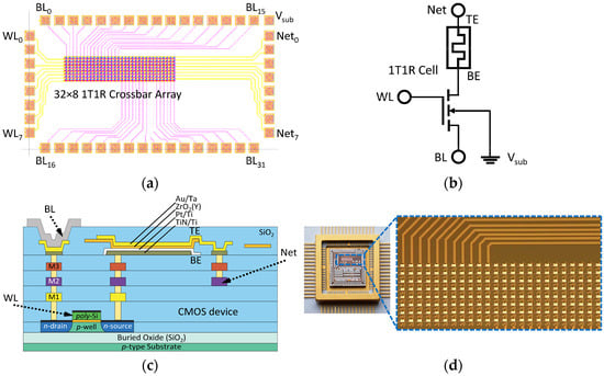
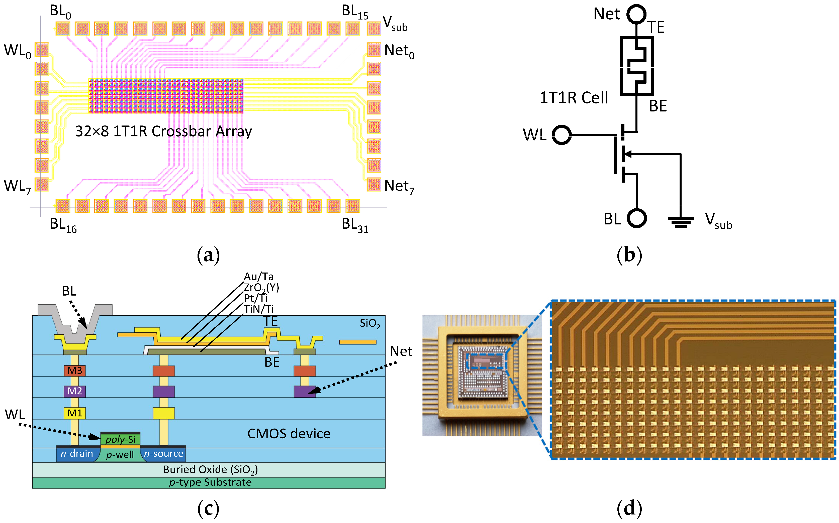
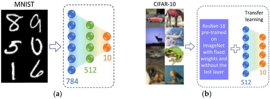
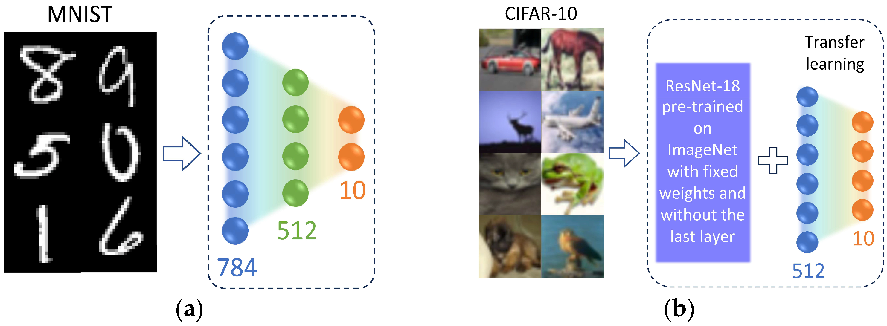
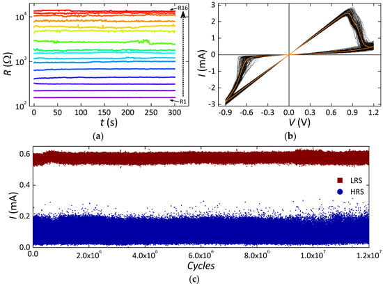
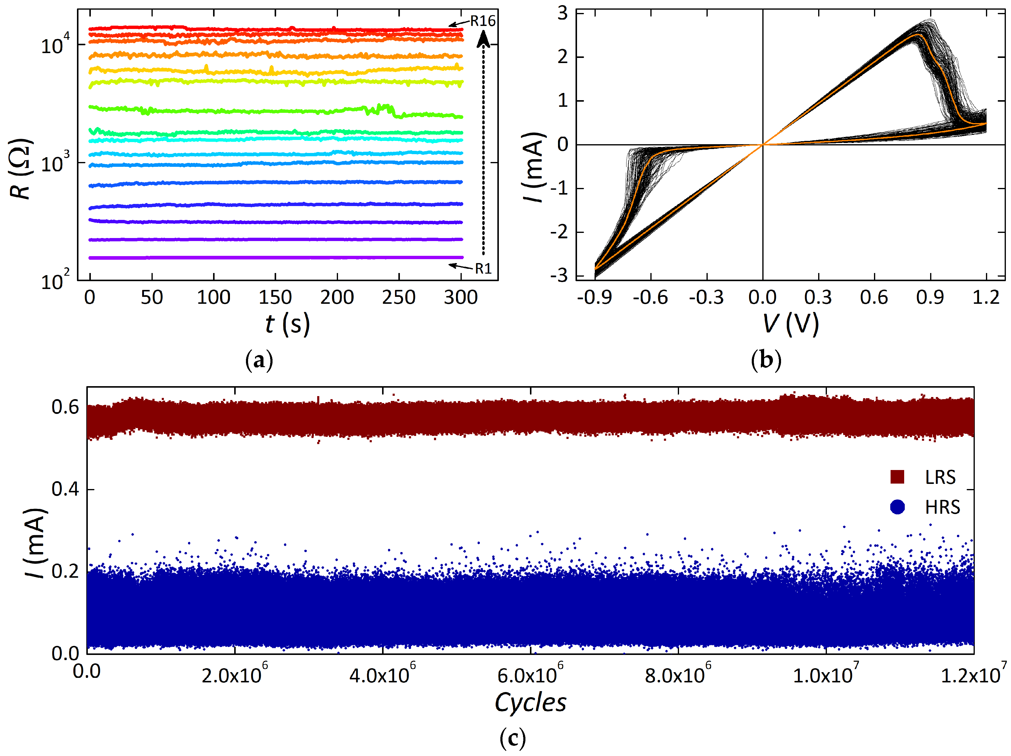
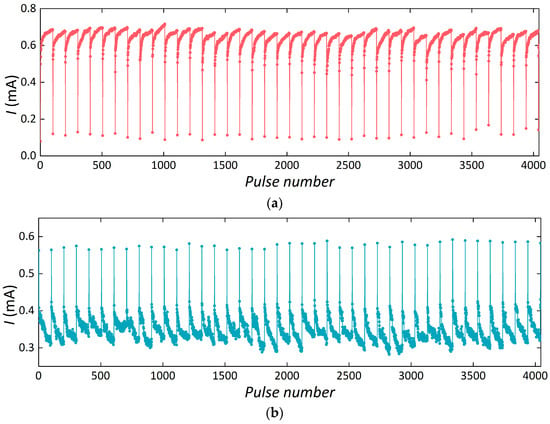
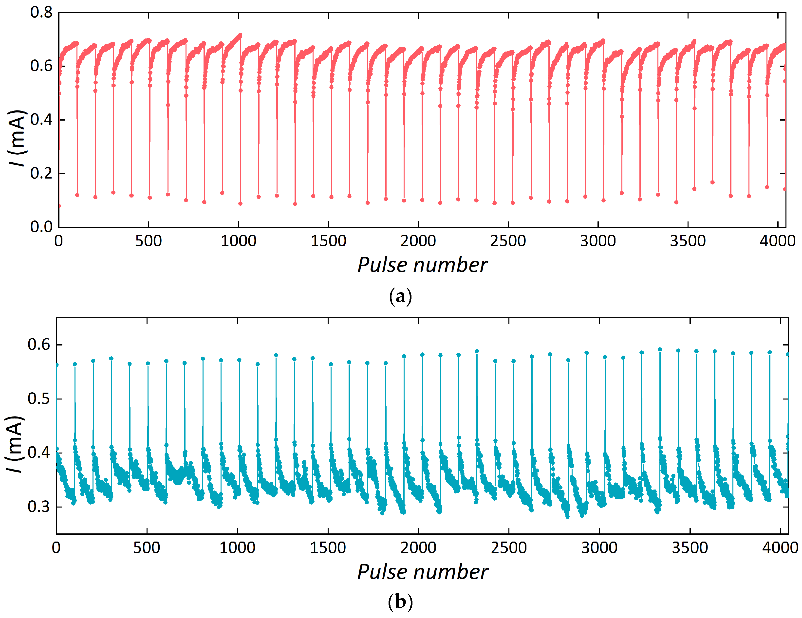
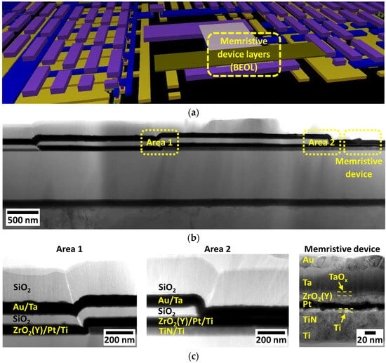
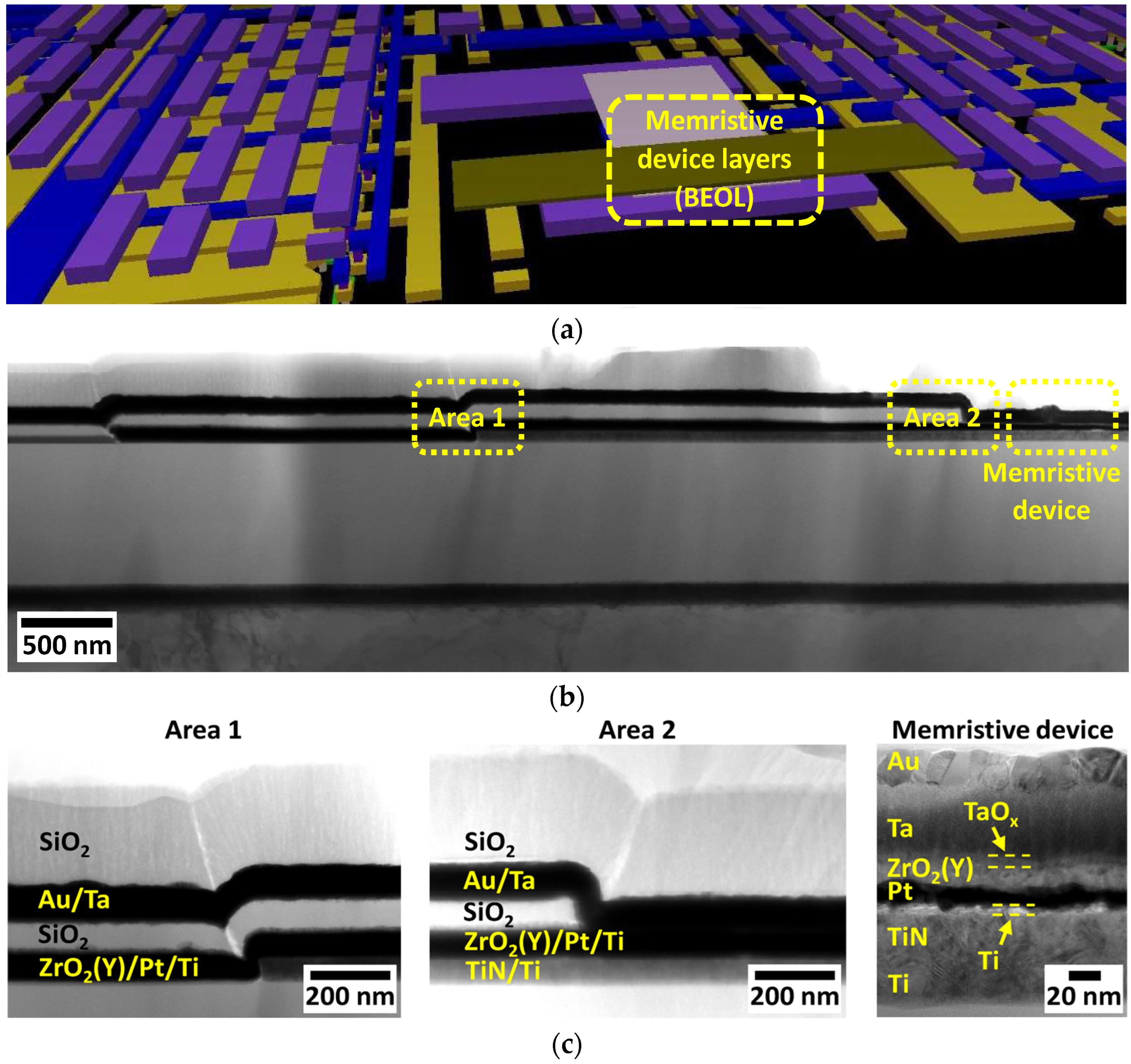
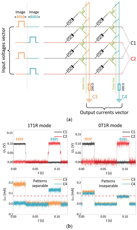
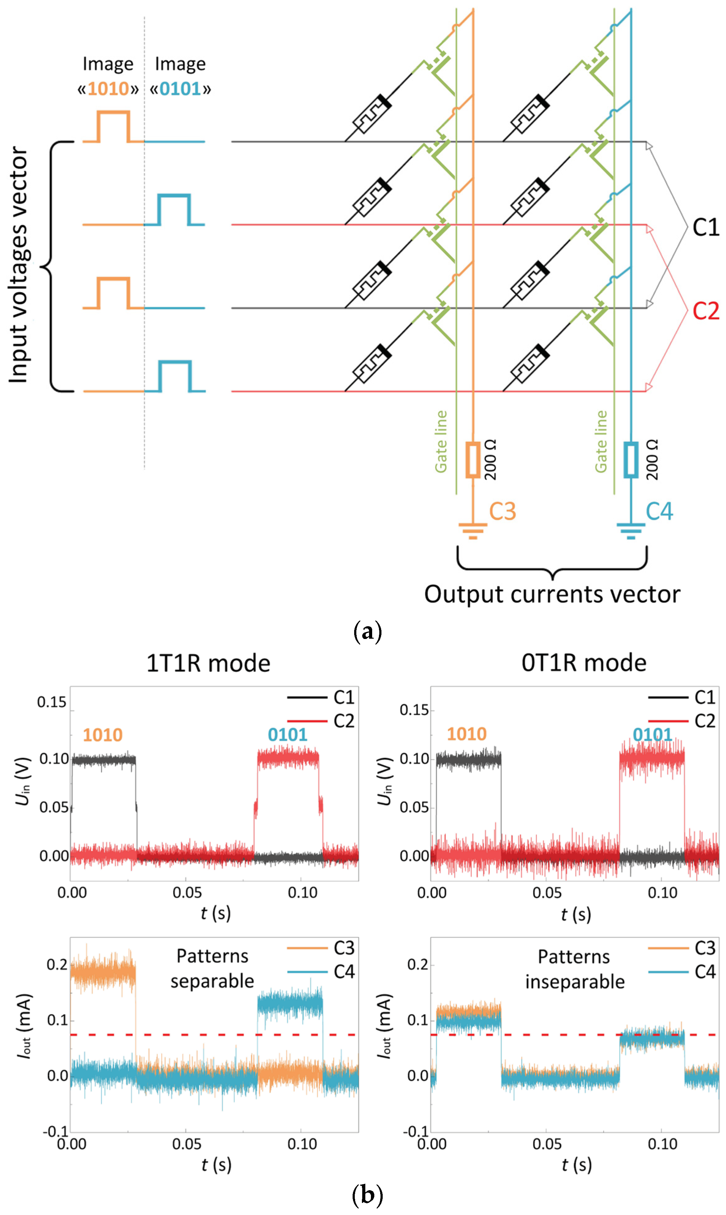
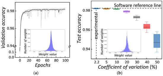
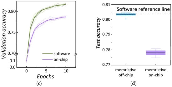
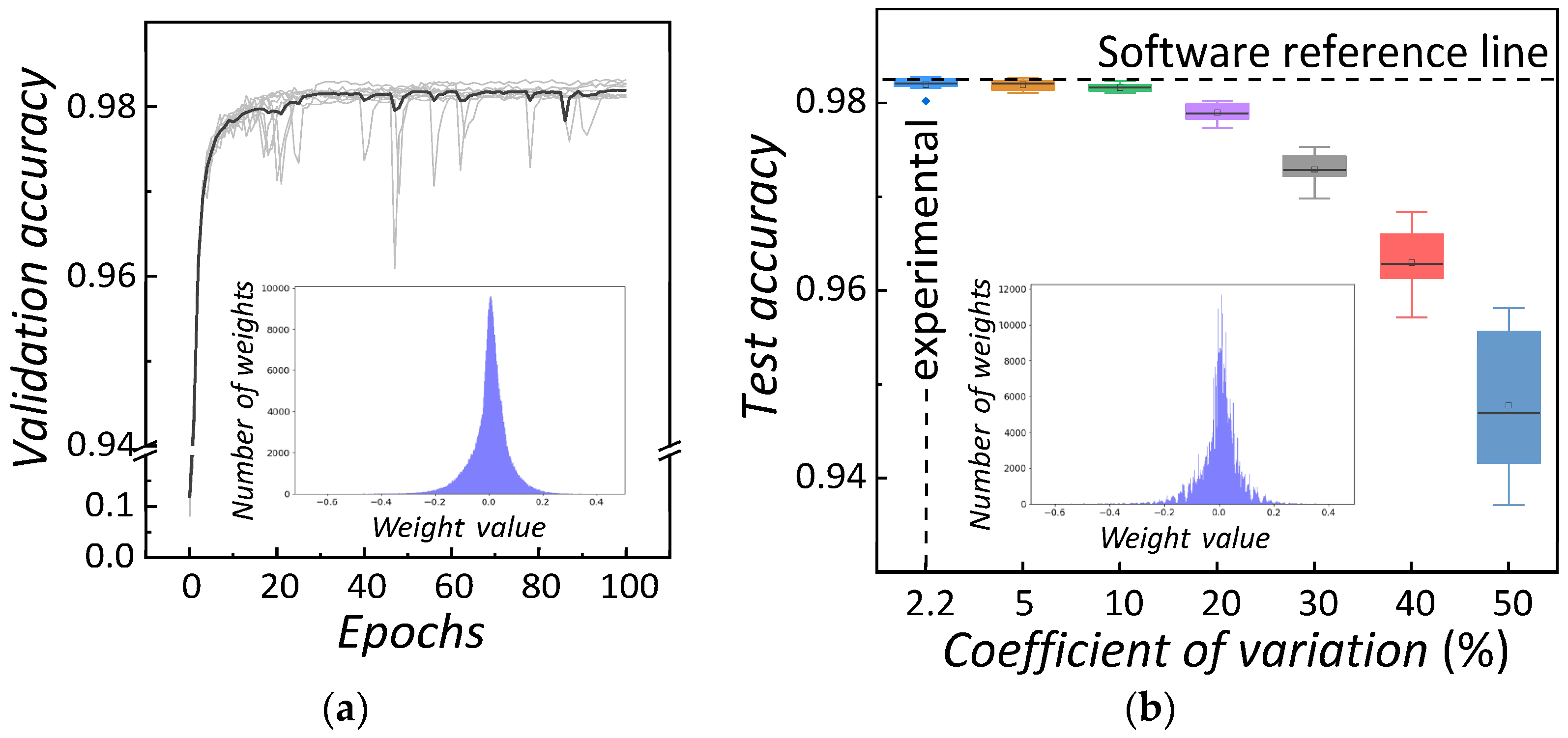
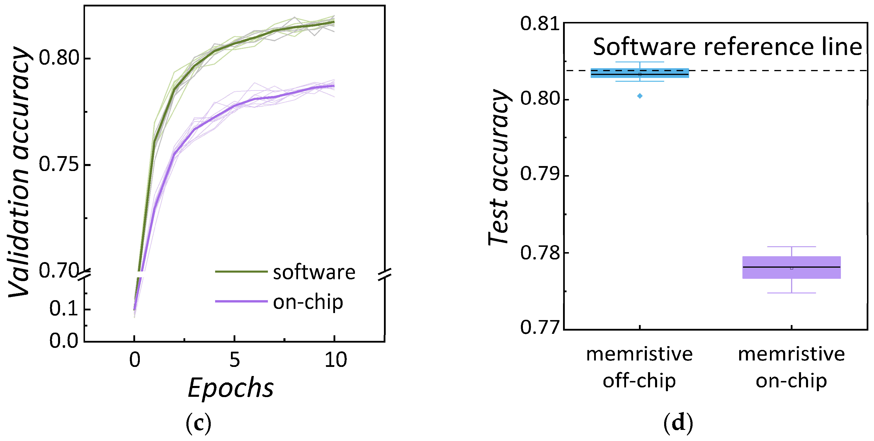
Disclaimer/Publisher’s Note: The statements, opinions and data contained in all publications are solely those of the individual author(s) and contributor(s) and not of MDPI and/or the editor(s). MDPI and/or the editor(s) disclaim responsibility for any injury to people or property resulting from any ideas, methods, instructions or products referred to in the content. |
© 2026 by the authors. Licensee MDPI, Basel, Switzerland. This article is an open access article distributed under the terms and conditions of the Creative Commons Attribution (CC BY) license.