


Abstract
This paper proposes an Active Gate Driver (AGD) for a DC–DC boost converter based on Silicon Carbide (SiC) power devices, in which surge voltage and ringing arise from their fast-switching characteristics. In this work, a practical and simple 4-bit logic AGD was proposed to adjust the gate resistance during the Miller interval of the SiC MOSFET. This helps suppress these effects and lowers the surge voltage and ringing stress on the power device. Experimental results demonstrate that the voltage overshoot decreases from 52 V to 22 V, corresponding to a reduction from 52% to 22% under a 100 V output condition, while the peak drain–source voltage decreases from 152 V to 122 V. The turn-off energy increases from 60.2 µJ to 76.9 µJ due to the slightly reduced switching speed. This trade-off represents the improvement in the comparison between transient suppression and switching loss. In addition, the voltage ringing is significantly attenuated. Although the modified switching strategy slightly increases switching loss, it effectively improves waveform quality and reduces voltage stress. These results confirm that the proposed AGD provides a simple and effective solution for improving the switching robustness and reliability of SiC-based DC–DC boost converters.
1. Introduction
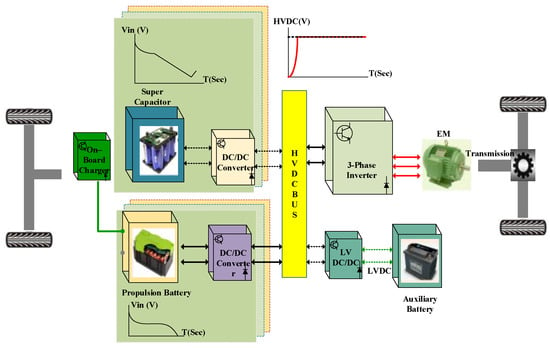
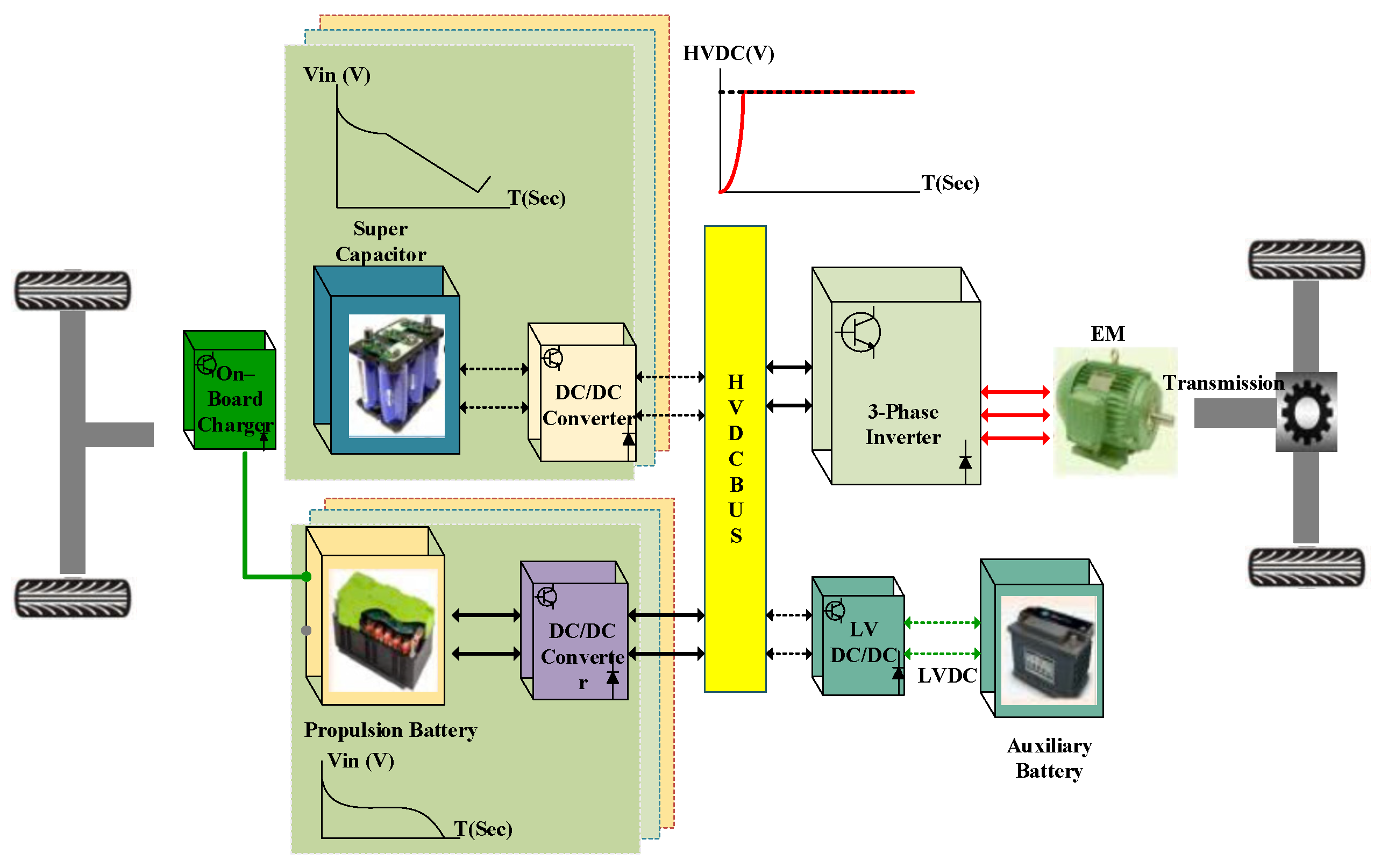
Recent surveys consistently report a clear trend toward adopting wide-bandgap (WBG) semiconductor devices, in particular SiC MOSFETs, SiC diodes, and gallium nitride (GaN) FETs for high-power DC–DC converters in electric vehicle (EV), as shown in Figure 1 [1,2,3]. SiC MOSFETs, as wide-bandgap (WBG) power devices, are particularly well suited for DC–DC converters [4,5,6,7]. From a material perspective, SiC has a bandgap energy of approximately 3.26 eV (compared with 1.1 eV for Si), a breakdown electric field of about 3 × 10⁶ V/cm (roughly an order of magnitude higher), and a thermal conductivity of about 3.7 W/cm⋅K (nearly 2.5 times the 1.5 W/cm⋅K of Si) [8,9]. These physical parameters enable a thinner drift layer while maintaining the voltage-blocking capability for ratings from 1.2 kV to 3.3 kV. Consequently, the specific on-state resistance Ron decreases significantly, and conductance losses at the same power level are much lower compared with Si-based MOSFETs and IGBTs [10,11].
Figure 1.
Block diagram of an electric vehicle powertrain [1].
However, the very fast switching behavior of SiC MOSFETs introduces several challenges in the power circuit. Therefore, the current design trend involves adopting AGD techniques, in which the gate-source voltage waveform is shaped for each switching phase to actively set dv/dt, di/dt, and the I–V trajectory within a desired operating region [12,13]. The fast-switching process, combined with parasitic inductance and capacitance in the power and gate loops, can easily lead to overvoltage, ringing, and self-turn-on (false turn-on or crosstalk) phenomena in power converters, which can be controlled using AGD [14,15,16,17]. Compared with AGD, fixed gate-driver circuits (a single RG value and a single VGS level) are no longer sufficient to fully exploit the potential of SiC MOSFETs in high-power converters [18,19]. To reduce voltage overshoot and enhance switching performance across various operating conditions, further studies investigated feedback-based AGD schemes [20]. Building on this idea, subsequent studies investigated various AGD methods, such as switching-trajectory optimization and stage-wise gate control, to achieve more accurate control of switching transients [21,22]. Other AGD implementations were further developed to improve the switching performance while, in turn, mitigating the voltage overshoot and switching losses [23,24]. In the meantime, various gate-driver topologies and design approaches were investigated to improve transient behavior and ensure reliable operation under high (dv/dt) conditions [25,26]. To balance surge voltage suppression and converter efficiency, programmable and digital AGD solutions were also documented in [27,28,29]. It shows that AGD technology for SiC MOSFET applications is still evolving. However, this programmable IC, which is just in the laboratory, is not yet suitable for industrial applications. On the other hand, the closed-loop gate-sensing and feedback-based AGD approaches have been developed in [30,31] to dynamically control switching transients and improve the trade-off between voltage-overshoot suppression and switching losses. The summary and comparison of the development and challenges of the previous study on AGD are presented in Table 1. Numerous AGD techniques have been proposed to improve the switching performance of SiC MOSFETs with complicated control.
Table 1.
Comparison of Representative AGD Techniques for SiC MOSFET Applications.
However, most studies have focused on inverter applications or require relatively sophisticated control structures. Furthermore, it lacks study on developing suitable AGD for DC–DC boost converter, where the high switching speed of SiC MOSFETs can still result in significant surge voltage and ringing due to the parasitic inductances in the power loop during turn-off transitions. In our work, the feasibility of an Active Gate Driver for mitigating these effects was verified through simulation studies [32]. Building upon this foundation, the present work develops and experimentally validates a practical AGD hardware system based on active gate-resistance control for reducing turn-off surge voltage and improving the operating performance of a DC–DC boost converter.
The rest of this paper is organized as follows. Section 2 describes the analysis of the gate driver for the SiC MOSFET in a DC–DC boost converter. The principles of the gate driver and surge voltage are analyzed. Section 3 presents simulation and experimental results of a DC–DC boost converter using SiC MOSFETs. Section 4 shows the simulation and experimental results. Section 5 discusses research results and related requirements. Finally, Section 6 concludes the paper with key findings and future research directions.
2. Analysis Turn-Off Transient of SiC MOSFET
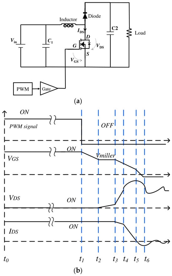
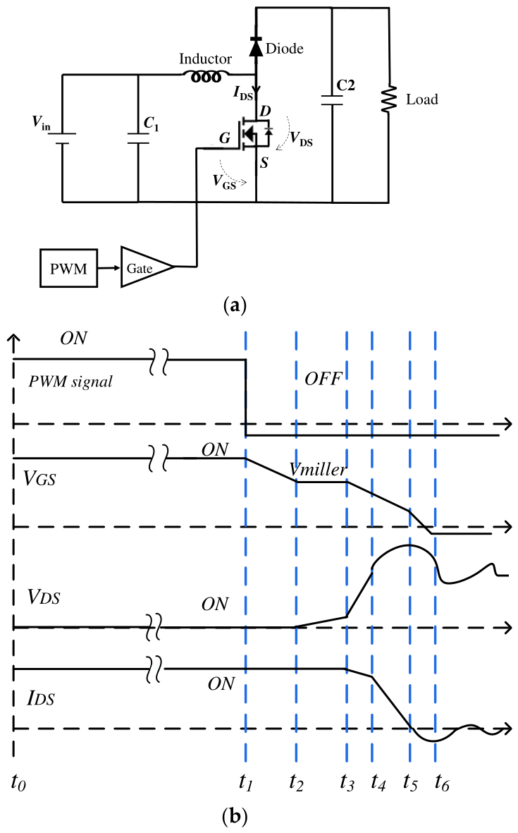
In boost-type converters, as shown in Figure 2a, high switching speed causes parasitic L-C elements and the MOSFET capacitances, which generate surge voltage and resonant ringing. Therefore, the SiC MOSFET switching transient was divided into characteristic time intervals. Based on this segmentation, the dependence of the switching speed on the AGD control parameters was analyzed. This relationship provides the foundation for designing and optimizing the gate-control strategy. This should provide a concise and precise description of the experimental results, their interpretation, and the experimental conclusions. The MOSFET’s turn-off process can be divided into characteristic time intervals, as illustrated in Figure 2b.
Figure 2.
Switching behavior of the SiC MOSFET: (a) DC–DC Boost converter; (b) corresponding switching waveforms.
- (1)
- − is the turn-off delay time. During this interval, the circuit discharges the input capacitance Ciss from its initial value down to the Miller level. The gate–source voltage VGS starts to decrease from Vdron but remains higher than Vmiller. The drain current and drain–source voltage stay almost unchanged: IDS ≈ I0, VDS ≈ Von.
- (2)
- − is the onset of the Miller plateau (turn-off). In this interval, the drain–source voltage VDS begins to increase from ID × RDS(on) toward ten percentage of its high value. The gate current primarily charges/discharges the Miller capacitance, CGD, while the drain current, IDS, remains approximately equal to the load current. The gate–source voltage VGS reaches the Miller level Vmiller and enters the turn-off Miller plateau. Immediately after this point, CGD starts to discharge, and VDS starts to rise.
- (3)
- is the drain–source voltage rise time region. This interval corresponds to the rising edge of VDS and is used to determine the turn-off dv/dt. The drain–source voltage increases from Von to a value close to Vbus, while the drain current remains approximately constant (IDS ≈ Io). The gate-source voltage VGS stands around the Miller plateau Vmiller. During this interval, VDS increases from low to high, which is used to calculate the turn-off dv/dt as in (1).
- (4)
- is the drain current fall time region. At t4, VDS has already risen to a high level. Then, VGS drops toward the threshold voltage Vth, which leads the drain–source current Ids to begin decreasing to a low level. During this interval, IDS falls from I0 to 0, and this segment is used to calculate the turn-off di/dt as in (2).
- (5)
- is the final turn-off region. The drain current is essentially zero (IDS ≈ 0), and the device is almost completely turned off. The gate-source voltage VGS continues to discharge toward Vdroff (0 V or a negative value), completing the turn-off process.
The SiC MOSFET switching edge rate is governed by gate-driver parameters, including the gate current IG, the parasitic capacitances CGD and CGS, the external gate resistance RG, and the driver voltage levels (Vdron, Vdroff). Among these factors, changing RG before and during the Miller interval provides the most practical and widely adopted control handle, since it can be tuned directly at the circuit level without altering the device structure or redesigning the gate driver.
3. Proposed Active Gate Driver for SiC MOSFET
In this study, the switching speed is regulated using a time-varying gate resistance rather than a fixed resistor. As shown in Figure 3, the proposed Active Gate Driver is configured with multiple parallel resistor branches, which are selectively activated during both the turn-on and turn-off transitions depending on the VGS condition. The proposed AGD method for a DC–DC boost converter does not employ a high gate resistance throughout the entire turn-off process as a conventional fixed gate resistor. Instead, the gate resistance is switched only for a short time during the Miller interval, when voltage overshoot is primarily generated. This achieves a better trade-off between voltage overshoot suppression and switching losses than a conventional fixed gate resistor.
Figure 3.
Proposed circuit of the Active Gate Driver method.
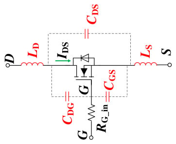
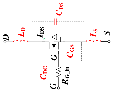
Figure 4 shows the MOSFET with parasitic inductance and capacitance elements. When VGS enters the Miller plateau region, where dv/dt and di/dt exhibit the highest sensitivity to the gate-driving strength, the effective gate resistance RG is intentionally increased to slow down the switching transition. In this manner, voltage overshoot is mitigated, and ringing is suppressed. Outside the Miller interval, RG is decreased to enhance the gate driving capability, thereby shortening the switching transient and reducing the switching energy losses Eon and Eoff.
Figure 4.
The switching waveforms of a variable gate resistance AGD.
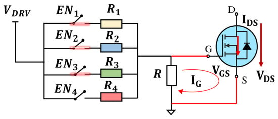
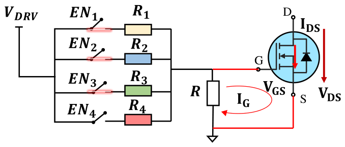
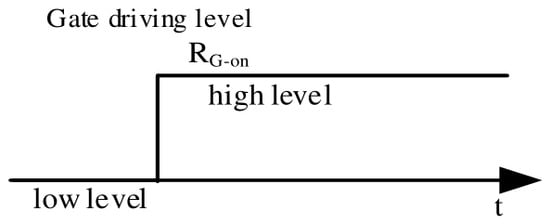
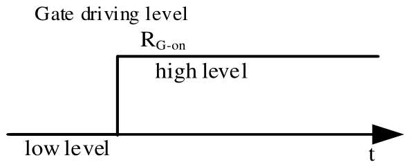
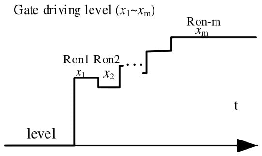
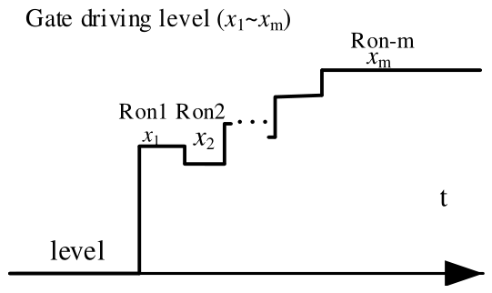
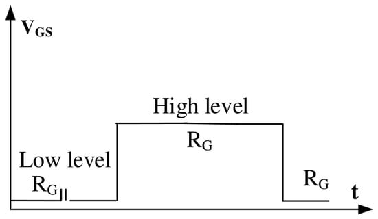
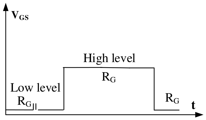
Figure 5 and Figure 6 conceptually compare the conventional fixed-RG-on gate drive with the proposed AGD approach, in which the effective turn-on resistance is stepwise adjusted via (Ron1…Ron-m) according to the control states (x1∼xm) to shape the switching transient. Table 2 lists the 16 gate-resistance combinations of the 4-bit Active Gate Driver. These combinations are selected and scheduled to optimize the MOSFET switching transient by shaping the gate current IG. The proposed AGD control is implemented by sequentially activating the resistor branches through the enable signals EN1–EN4 according to the gate-voltage operating regions of the SiC MOSFET. During the initial switching interval, a lower equivalent gate resistance is selected to provide a higher gate current and accelerate the switching process. As the gate voltage approaches the Miller plateau region, the equivalent gate resistance is increased to limit the gate current, thereby reducing dv/dt, di/dt, and the associated voltage overshoot. The gate resistance is lowered once again to finish the switching transition as quickly as possible after the Miller interval. Through this time-varying gate-resistance profile, the proposed AGD achieves a balance between surge-voltage suppression and switching-loss reduction.
Figure 5.
Normal gate drive.
Figure 6.
Active gate drive (AGD).
Table 2.
Switching configurations and corresponding gate resistance values of the 4-bit Active Gate Driver.
4. Simulation and Experimental Results
To verify the effectiveness of the proposed AGD technique, this section presents a comparative analysis between a conventional gate driver and the AGD implementation in a high-efficiency DC–DC boost converter, using simulation and experiment. Table 3 lists the power components in simulation and experiment.
Table 3.
Components in simulation, experiment.
4.1. Simulation Results
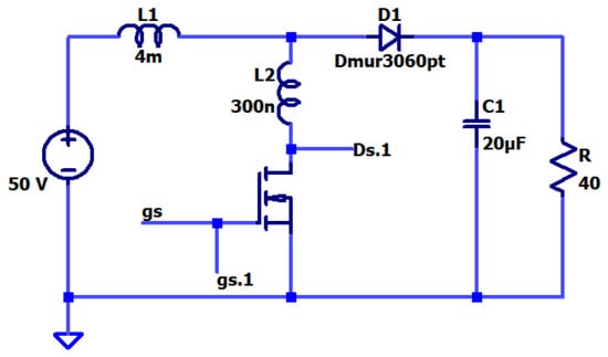
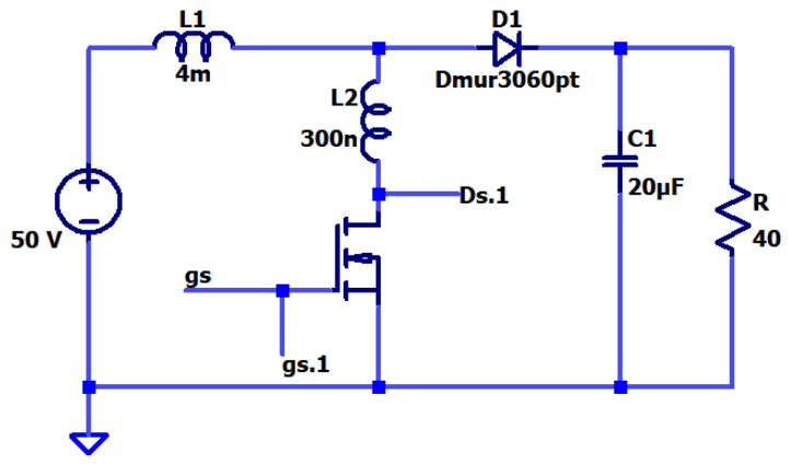
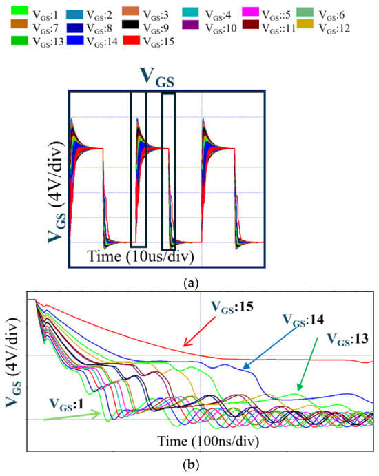
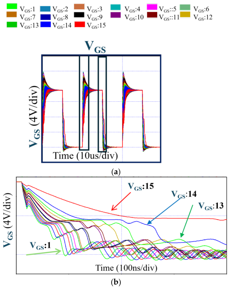
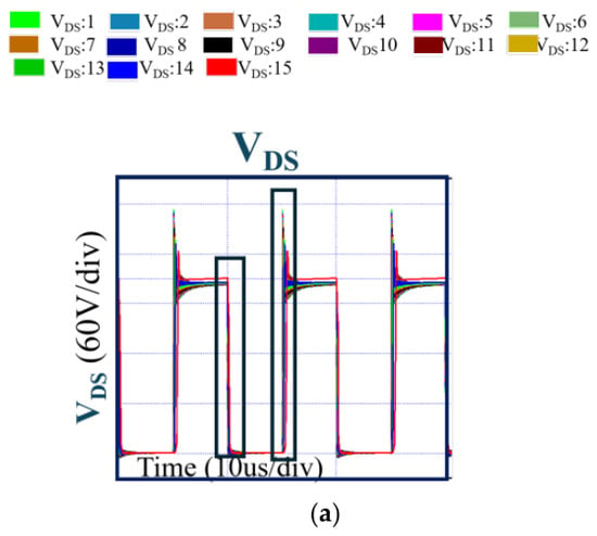
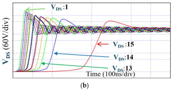
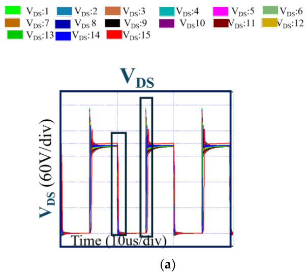
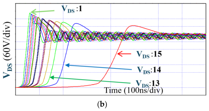
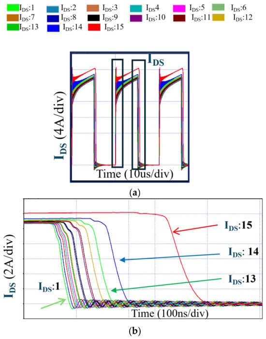
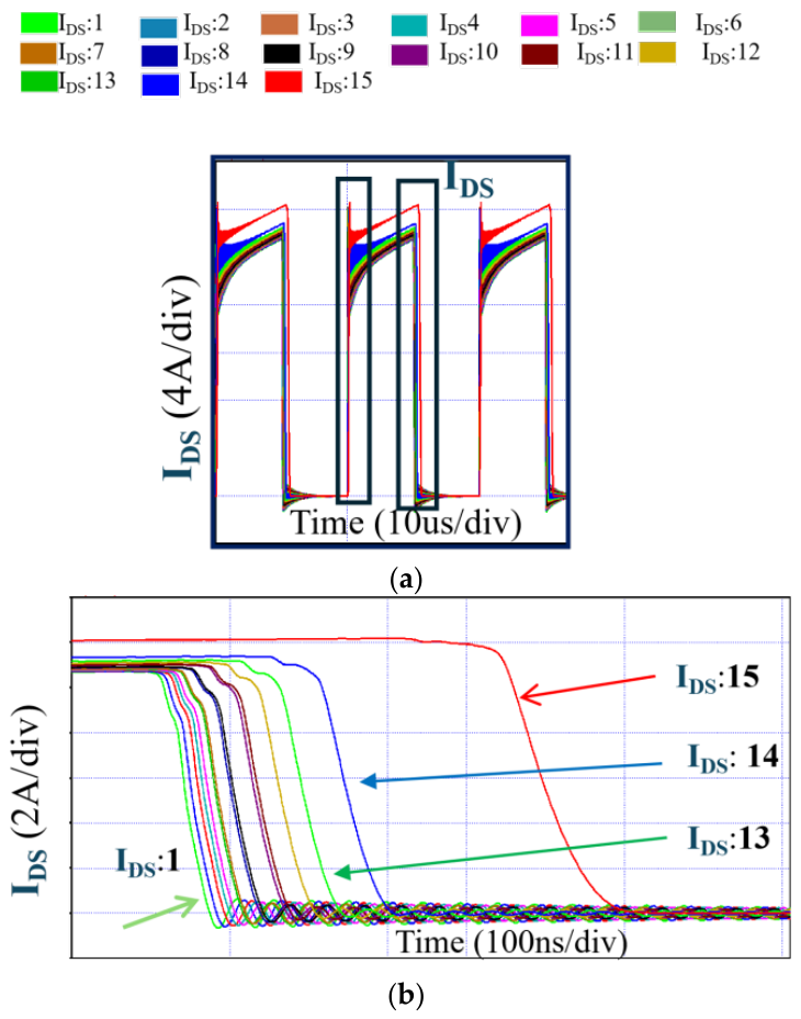
Table 4 displays the detailed parameters of the test bench and measurement equipment used in the test. The DC–DC boost converter increases the input voltage from 200 V to the output voltage of 400 V. Switching frequency is 100 kHz. Figure 7 shows the waveform representation under the conventional scheme. In this baseline case, the external gate resistance over the range RG = 10.8 to 100 Ω was applied while keeping the gate command (0–15 V) and the power-stage parameters unchanged. VGS, VDS, and IDS around the turn-on/turn-off commutation intervals were extracted. As shown in Figure 8, the LTspice schematic is used for simulation. Figure 9, Figure 10 and Figure 11 and Table 4 confirm that a conventional fixed-RG gate drive imposes an inherent and unfavorable trade-off. As the gate resistance RG increases from 10.8 Ω to 100 Ω, the conventional fixed-RG gate drive significantly suppresses the switching slew rates during both turn-on and turn-off transitions. Specifically, dv/dt (on) decreases from 6.94 to 2.08 V/ns, while dv/dt (off) is reduced more sharply from 17.9 to 3.5 V/ns.
Table 4.
Boost DC–DC circuit specifications.
Figure 7.
Conventional PWM control.
Figure 8.
LTspice schematic used for simulation.
Figure 9.
VGS waveforms for conventional fixed-RG drive: (a) gate-source voltage VGS; (b) VGS zoomed-in turn-off transient.
Figure 10.
VDS waveforms for conventional fixed-RG drive: (a) drain–source voltage VDS; (b) VDS zoomed-in turn-off transient.
Figure 11.
IDS waveforms for conventional fixed-RG drive: (a) drain–source current IDS; (b) IDS zoomed-in turn-off transient.
Table 5 shows the summary of the effects of RG on switching characteristics when changing fixed gate resistance. Despite this pronounced reduction in dv/dt, the peak VDS overshoot is only moderately mitigated, decreasing from 585.6 V to 486.7 V (approximately 16.9%). However, this comes at the cost of substantially prolonged switching intervals (toff: 85.2 → 441.9 ns) and a dramatic increase in switching energy. Notably, at RG ≈ 21.9 Ω, dv/dt is already reduced (turn-on 18.9%, turn-off 31.6%), and overshoot decreases by 7.35%, yet Esw increases by 43.8%, indicating that slowing the device throughout the entire transient using a larger fixed RG is energetically inefficient.
Table 5.
Summary of the effects of RG on switching characteristics when changing fixed gate resistance.
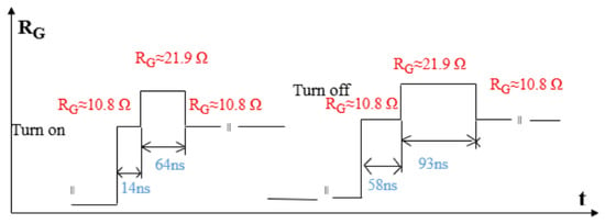
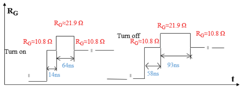
Instead of using a single gate resistance, AGD selectively intervenes around the Miller/voltage-transition interval by dynamically switching the effective gate resistance over time. Specifically, a strong drive level with RG,low ≈ 10.8 Ω was applied to preserve fast gate-charge transfer and limit Eon/Eoff, then temporarily switch to RG,Miller ≈ 21.9 Ω during the Miller plateau to reduce dv/dt, suppress VDS overshoot, and damp commutation-loop ringing. After the Miller interval, the gate resistance returns to RG, low for the remaining switching stages, as shown in Figure 12. Therefore, the increased gate resistance is applied only during the critical transition interval, limiting the increase in switching loss while preserving the surge-voltage suppression capability of the proposed AGD.
Figure 12.
Gate control patterns used in simulations.
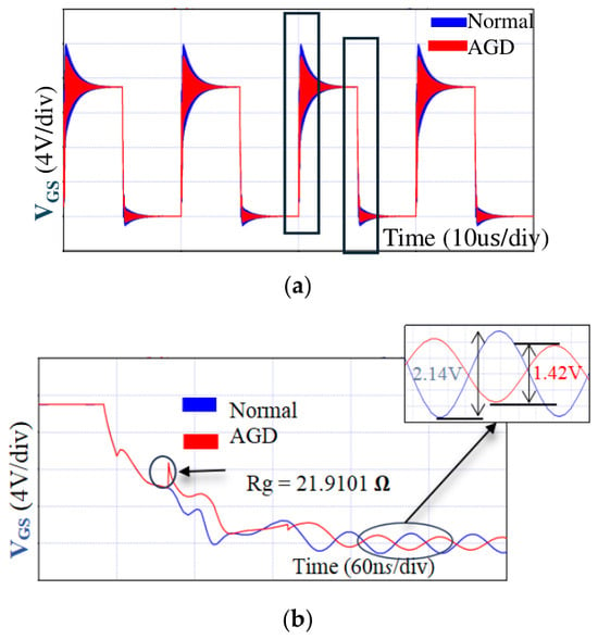
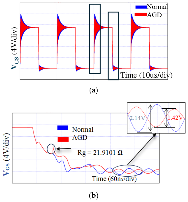
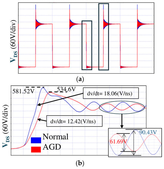
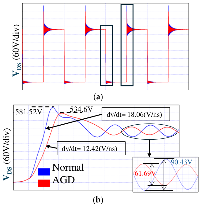
Based on the identified Miller-region, the simulation scenario was conducted following the principle of intervening only during the voltage-transition interval. The Miller interval is first identified from the measured VGS waveform and then used to define the switching schedule of the proposed AGD. During this interval, the gate charge is predominantly transferred into CGD, and VDS changes rapidly. Consistent with the VDS waveforms, this time window corresponds to the steep VDS rising/falling edges and the most pronounced propensity for ringing. Accordingly, the AGD does not employ a fixed RG; instead, it time-variably switches the effective gate resistance. At the beginning of the transition, a low gate resistance was applied (RG,low ≈ 10.8 Ω) to accelerate gate-charge injection, maintain a short switching interval, and avoid excessive growth of Eon upon entering the marked Miller window, it temporarily switch to a higher resistance (RG Miller ≈ 21.9 Ω) to soften the voltage transition, thereby reducing dv/dt, lowering VDS overshoot, and damping switching-loop ringing. After the device exits the plateau, the AGD returns to RG,low for the remaining sub-stages to prevent unnecessary prolongation of the turn-on/turn-off process. In Figure 13, the VGS waveforms confirmed that the AGD intervenes only within the Miller window (i.e., the nearly flat plateau) by temporarily switching to RG Miller ≈ 21.9 Ω. Then it returns to a low gate resistance for the remaining sub-stages. When the AGD is activated within the Miller window, it clearly softens the VDS transition, as shown in Figure 14. During turn-on, the dv/dt decreases from 6.82 to 5.56 V/ns (≈18.5%), and the VDS ringing amplitude is reduced from 22.6 to 15.9 V (≈30%). During turn-off, the improvement is more pronounced: the dv/dt decreases from 18.06 to 12.42 V/ns (≈31%), the peak VDS drops from 581.52 to 534.6 V, resulting in a 26% reduction in the surge voltage from 181.5 V to 134.6 V. In addition, the ringing amplitude decreases from 90.43 to 61.69 V (≈32%).
Figure 13.
Comparison of VGS waveforms between the conventional gate drive and the AGD: (a) gate-source voltage VGS; (b). VGS zoomed-in turn-off transient.
Figure 14.
Comparison of VDS waveforms between the conventional gate drive and the AGD: (a) drain–source voltage VDS; (b). VDS zoomed-in turn-off transient.
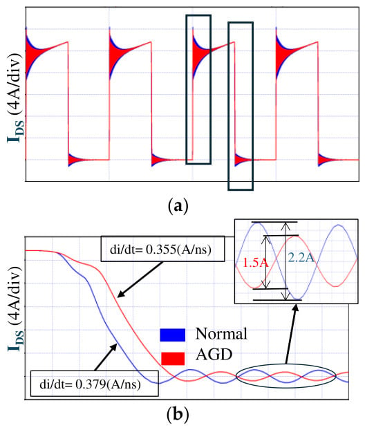
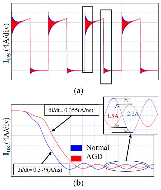
As shown in Figure 15, the current response reflects the reduced switching aggressiveness achieved by the proposed AGD. During turn-on, the AGD reduces di/dt from 0.722 to 0.564 A/ns (≈22%) and decreases the IDS ringing amplitude from 7.64 to 5.36 A (≈30%). During turn-off, the IDS ringing amplitude is further reduced from 2.2 to 1.5 A (≈32%), while di/dt changes only slightly from 0.379 to 0.355 A/ns (≈6%). These results confirm that the AGD effectively suppresses current oscillations while maintaining a comparable switching speed.
Figure 15.
Comparison of IDS waveforms between the conventional gate drive and the AGD: (a) drain–source current IDS; (b). IDS zoomed-in turn-off transient.
The simulation results show that activating the AGD specifically within the Miller window (temporarily increasing RG to approximately 21.9 Ω while maintaining a low RG outside the Miller interval) selectively softens the switching transition. As a result, the AGD reduces dv/dt and di/dt and markedly suppresses overshoot and ringing in both VDS and IDS, with the most pronounced improvement during turn-off.
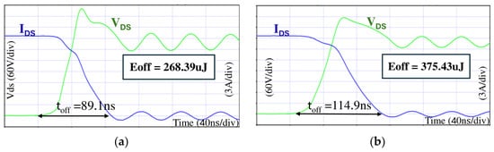
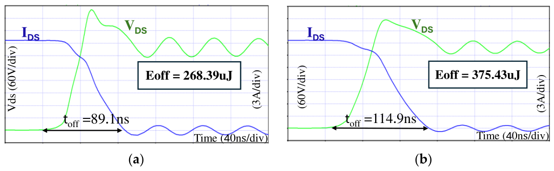
The switching loss and transition-time comparison between the fixed gate resistance method and the proposed AGD is presented in Figure 16. With a fixed gate resistance (RG = 10.79 Ω), the device exhibits faster switching, with shorter turn-off (toff ≈ 89.1 ns), resulting in lower switching losses (Eoff = 268.39 μJ). However, as discussed previously, this fast transition leads to significant voltage overshooting and ringing.
Figure 16.
Comparison of SiC MOSFET switching losses under fixed gate resistance and two-step AGD control: (a) fixed gate resistance (RG = 10.8 Ω); (b) two-step AGD control.
In contrast, the proposed AGD adaptively modifies the gate resistance during the switching process. The transitions are intentionally slowed (toff ≈ 114.9 ns), leading to higher switching losses (Eoff = 375.43 μJ). Nevertheless, the reduced dv/dt and di/dt effectively suppress overshoot and oscillations. These results highlight a clear trade-off between switching loss and waveform quality, where the AGD improves stability of the power converter.
4.2. Experimental Results
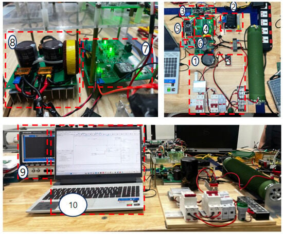
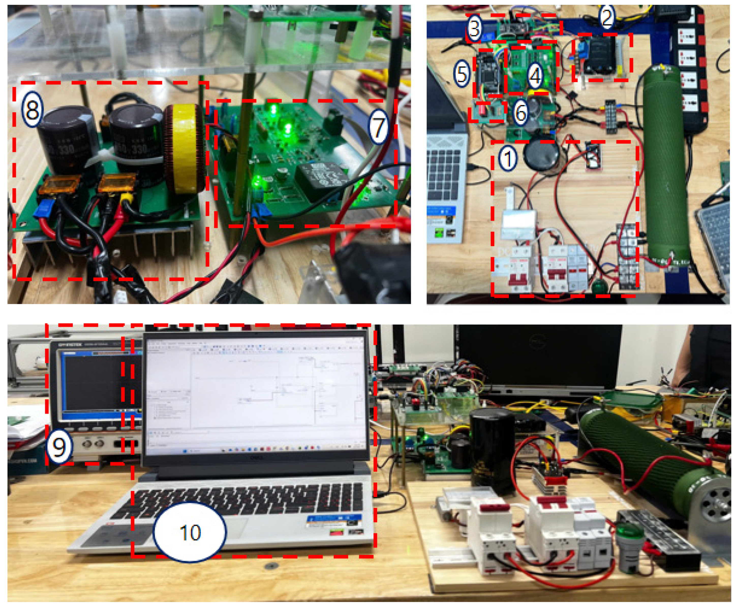
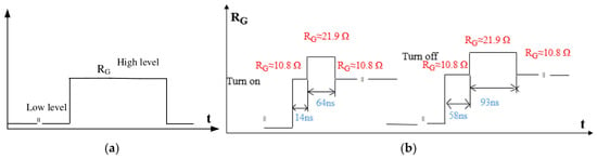
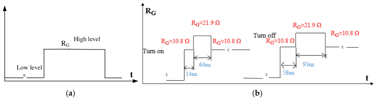
A boost-converter test bench is configured as shown in Figure 17. The operating condition is summarized in Table 6. The converter is operated at Vin = 50 V (±1%), fs = 100 kHz, and D = 50% to obtain Vout ≈ 100 V with a 100 Ω load (≈1 A). These settings provide a consistent baseline for evaluating the impact of AGD on switching transients and device stress. To assess the impact of gate-driving methods on switching characteristics, the experimentally implemented approaches, including constant and two-level-gate resistance, are illustrated in Figure 18.
Figure 17.
Experimental system: (1) rectifier circuit; (2) 5 V-AGD power supply circuit; (3) MCU; (4) AGD circuit; (5) FPGA; (6) DIP switch circuit; (7) boost converter; (8) measurement circuit; (9) oscilloscope; (10) computer.
Table 6.
Components of experiment.
Figure 18.
Gate pattern for switching control in experiment: (a) normal gate using fixed gate resistance; (b) gate pattern in proposed AGD control.
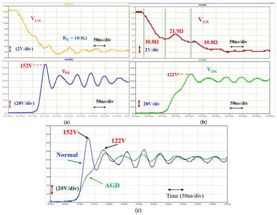
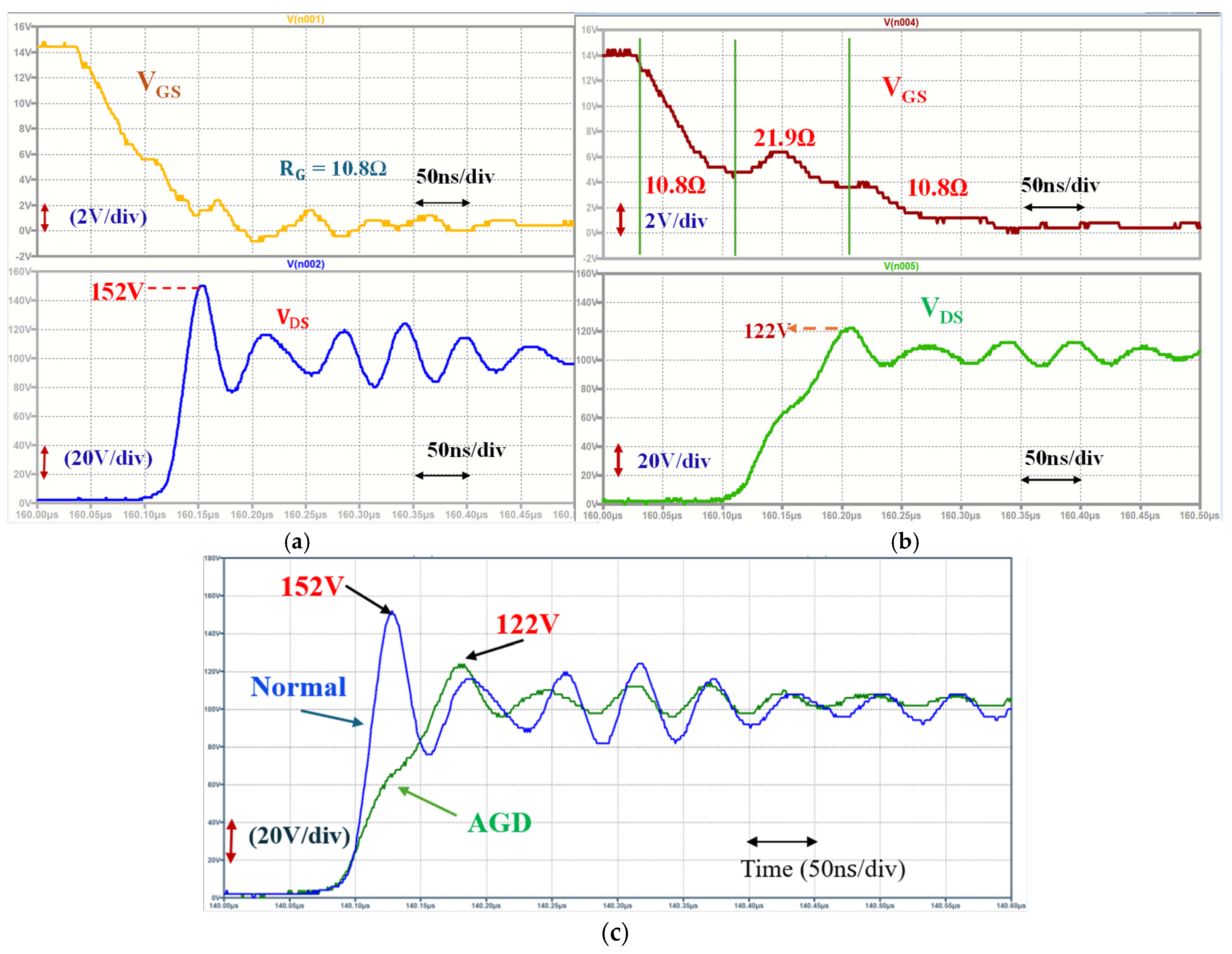
The experimental turn-off results of the SiC MOSFET demonstrate that Miller-region gate-resistance modulation provides a noticeable improvement in voltage stress and switching ringing compared with the conventional fixed-resistance gate driver. Figure 19 shows the experimental turn-off waveforms of the SiC MOSFET under a 50 V input and 100 V output condition. With the conventional gate driver (RG = 10.8 Ω), the drain–source voltage rises rapidly during turn-off. It reaches a peak value of 152 V. Since the steady-state blocking voltage is approximately 100 V, the corresponding voltage overshoot is about 52 V. A relatively large ringing amplitude is also observed after the switching transition.
Figure 19.
Comparison of SiC MOSFET switching waveforms under fixed gate resistance and two-step AGD control: (a) under fixed gate resistance (RG = 10.8 Ω); (b) two-step AGD control; (c) drain–source voltage comparison between two gate drivers.
To reduce the surge voltage, the proposed AGD temporarily increases the gate resistance to 21.9 Ω during the Miller interval. As shown in Figure 19b, the peak VDS decreases to 122 V, corresponding to an overshoot of 30 V. Compared with the conventional gate driver, the overshoot is reduced by 57.7%. The waveform indicates a smoother turn-off process when the proposed AGD is applied. However, the slower voltage transition increases turn-off energy. The measured Eoff increases from 60.2 µJ to 76.9 µJ. This result is expected because a larger gate resistance slows down the switching transition. Although Eoff increases, the reduction in voltage overshoot and dv/dt helps reduce the electrical stress on the device.
These results confirm that increasing gate resistance during the Miller region is an effective way to suppress the turn-off transient. The proposed method reduces voltage overshoot and ringing without requiring additional sensors or complex control circuits.
5. Discussion
The simulation results at an output of 400 V showed that the proposed AGD can reduce the surge voltage during the turn-off transient. By adjusting the switching speed at the Miller interval, the peak VDS drops from 581.52 V to 534.6 V, reducing the surge voltage by 26%, from 181.5 V to 134.6 V. In addition, the ringing amplitude decreases from 90.43 V to 61.69 V (≈32%). During the Miller interval, the proposed AGD temporarily increased RG to approximately 21.9 Ω while maintaining a low RG outside of that. Therefore, the AGD achieved softens the switching transition. As a result, the AGD reduces dv/dt and di/dt and markedly suppresses overshoot and ringing in both VDS and IDS, with the most pronounced improvement during turn-off. In addition, the switching loss and transition time comparison between the fixed gate resistance method and proposed AGD was provided. With a fixed gate-resistance (RG = 10.79 Ω), the device exhibits faster switching, with shorter turn-off (toff ≈ 89.1 ns), resulting in lower switching losses (Eoff = 268.39 μJ). However, as discussed previously, this fast transition leads to significant voltage overshooting and ringing. The proposed AGD adaptively modifies the gate resistance during the switching process. The transitions are intentionally slowed (toff ≈ 114.9 ns), leading to higher switching losses (Eoff = 375.43 μJ). It shows that there is a compensation between switching loss and surge voltage.
Furthermore, the experimental results indicate that the proposed AGD can effectively suppress surge voltage in comparison to the conventional fixed gate resistance approach, reducing the overshoot from 52 V to 22 V for the peak drain–source voltage from 152 V to 122 V. This strengthens the novelty of the paper in designing a 4-bit logic AGD and applying it to a DC–DC boost converter as the main contribution. The behavior is mainly attributed to the application of the proposed AGD during the Miller interval, which reduces surge voltage and limits the excitation of parasitic resonances. As a result, the peak voltage stress and oscillation amplitude are both reduced. The experimental waveforms also show a smoother turn-off current transition. However, the slower switching transition increases the turn-off energy from 60.2 µJ to 76.9 µJ. This result reflects the trade-off between transient suppression and switching loss. Overall, the proposed AGD balances switching loss and voltage stress by combining a standard gate driver integrated circuit (IC) with a 4-bit logic of variable resistors in a practical implementation. The experiment was conducted at 100 V due to the equipment’s current-conditioning limitations, but it confirmed the behavior and effectiveness of the proposed AGD, consistent with the simulation and theory.
Since the optimal gate resistance depends on the power converter’s operating conditions, particularly the switching current, the proposed AGD method is incorporated into the multiple gate-resistance method to provide the flexibility needed for different operating conditions. In this work, the gate-resistance values were predetermined to experimentally validate the proposed AGD hardware with an operating condition of the DC–DC boost converter. By measuring VGS, the Miller interval can be specified to tune the optimal gate pattern for each load condition. In addition, the switching current of the power converter will be measured under closed-loop control to verify optimal AGD values across different operating conditions to continue developing this research in the future.
As discussed above, the proposed AGD focused on a short time around the Miller interval. However, some very fast-switching SiC MOSFETs with very small input gate-source capacitance have a very short Miller interval. Even if there is still has a chance for AGD during a short window before the Miller interval, AGD faces challenges in effectively affecting that window. It requires high accuracy and bandwidth, which may limit its application. This point needs further investigation into the next research.
It should be noted that the magnitude of voltage overshoot is strongly influenced by the parasitic inductance of the power loop. Therefore, different converter layouts and soldering may exhibit different absolute overshoot levels. Since the proposed AGD is applied during the Miller interval, the surge-voltage suppression mechanism remains effective under different parasitic inductance conditions with a suitable optimal gate pattern. The effectiveness of the proposed AGD depends on the appropriate selection of gate-resistance combinations and switching schedules. These parameters may require re-optimization when the converter operating conditions, device ratings, or parasitic parameters change. Furthermore, the proposed AGD introduces additional switching elements compared with a conventional fixed-resistance gate driver, providing flexibility for combining software and hardware solutions.
6. Conclusions and Future Work
This paper proposed a 4-bit logic Active Gate Driver with variable gate resistance for improving the switching behavior of SiC MOSFETs in a DC–DC boost converter. By adjusting the gate resistance during only a short-time Miller interval, the proposed method effectively suppresses voltage overshoot and switching oscillations. Both simulation and experimental results demonstrate improved switching performance and reduced voltage stress across the power devices. In simulation, the surge voltage decreased from 581.52 V to 534.6 V, resulting in a 26% reduction from 181.5 V to 134.6 V. The ringing amplitude decreased from 90.43 V to 61.69 V (≈32%). Under the experimental condition of a 50 V input and 100 V output boost converter, the proposed AGD reduced the peak drain–source voltage from 152 V to 122 V, corresponding to the overshoot reduction from 52% to 22% (52 V to 22 V). In addition, it resulted in a noticeable attenuation of voltage ringing. These results confirm the effectiveness of the proposed gate-resistance modulation strategy.
Compared with the conventional fixed gate resistance method, the proposed AGD suppresses surge voltage by intentionally increasing the gate resistance only during the Miller interval, thereby slightly reducing switching speed during this critical period. The proposed AGD achieves smoother switching transitions and lower voltage stress. Although the turn-off energy increases from 60.2 µJ to 76.9 µJ due to the reduced switching speed, this trade-off is acceptable considering the significant improvement in comparison between transient suppression and switching loss. Overall, the proposed AGD method provides a practical compromise between switching performance, voltage reliability, and switching loss for SiC-based power converters. It provides a simple, effective solution for enhancing the reliability and robustness of high-speed power electronic systems.
In future work, this research will continue to develop a closed-loop control to verify the proposed AGD for variable operating conditions. The optimal AGD that maintains high switching performance while reducing the surge voltage can be discussed and confirmed using feedback control.
Author Contributions
Conceptualization, V.-L.P. and T.-H.N.-T.; methodology, V.-L.P. and T.-H.N.-T.; supervised the experiments of the research, V.-L.P.; validation, V.-L.P. and T.-H.N.-T.; formal analysis, V.-L.P. and T.-H.N.-T.; investigation, V.-L.P. and T.-H.N.-T.; writing, review, and editing, V.-L.P. and T.-H.N.-T.; funding acquisition, V.-L.P. All authors have read and agreed to the published version of the manuscript.
Funding
This research is supported by funding by Hanoi University of Science and Technology (HUST) under project number T2024-TĐ-021.
Data Availability Statement
The original contributions presented in this study are included in the article. Further inquiries can be directed to the corresponding author.
Acknowledgments
We would like to thanks to the support from members of research group Energy Management and Conversion (EMClab), Laboratory of Power Electronic Converters, Department of Automation Engineering, School of Electrical and Electronics Engineering, Hanoi University of Science and Technology, Hanoi, Vietnam.
Conflicts of Interest
The authors declare no conflicts of interest.
Abbreviations
The following abbreviations are used in this manuscript:
| AGD | Active Gate Driver |
| WBG | Wide Bandgap |
| SiC | Silicon Carbide |
| EV | Electric Vehicle |
| DC–DC | Direct Current–Direct Current |
References
- Chakraborty, S.; Vu, H.; Hasan, M.M.; Tran, D.; El Baghdadi, M.; Hegazy, O. DC–DC converter topologies for electric vehicles, plug-in hybrid electric vehicles, and fast charging stations: State of the art and future trends. Energies 2019, 12, 1569. [Google Scholar] [CrossRef] [Scilit]
- Rasul, A.; Teixeira, R. Silicon carbide converter design: A review. Energies 2025, 18, 2140. [Google Scholar] [CrossRef] [Scilit]
- Kumar, S.; Jammeh, S.; Samb, R.; Singh, A. Efficient DC–DC power converters for fuel-cell electric vehicles: A qualitative assessment. IET Power Electron. 2024, 17, 3166–3204. [Google Scholar] [CrossRef] [Scilit]
- Noge, Y.; Shoyama, M. High bandwidth active gate driver for simultaneous reduction of switching surge and switching loss of SiC-MOSFET. IEEJ J. Ind. Appl. 2023, 12, 384–391. [Google Scholar] [CrossRef] [Scilit]
- Fatahilah, M.F.; Strempel, K.; Yu, F.; Vodapally, S.; Waag, A.; Wasisto, H.S. 3D GaN nanoarchitecture for field-effect transistors. Micro Nano Eng. 2019, 3, 59–81. [Google Scholar] [CrossRef] [Scilit]
- Zhang, Z.; Guo, B.; Wang, F.; Jones, E.A.; Tolbert, L.M.; Blalock, B.J. Methodology for wide band-gap device dynamic characterization. IEEE Trans. Power Electron. 2017, 32, 9307–9317. [Google Scholar] [CrossRef] [Scilit]
- Sojka, P.; Pipiska, M.; Frivaldsky, M. GaN power transistor switching performance in hard-switching and soft-switching modes. In Proceedings of the 2019 20th International Scientific Conference on Electric Power Engineering (EPE), Kouty nad Desnou, Czech Republic, 17–15 May 2019. [Google Scholar]
- Alves, L.F.S.; Lefranc, P.; Jeannin, P.O.; Sarrazin, B. Review on SiC-MOSFET devices and associated gate drivers. In Proceedings of the IEEE International Conference on Industrial Technology, Lyon, France, 19–22 February 2018; pp. 824–829. [Google Scholar]
- Hofsajer, I.W. A review of the experimental performance of turn-off methods in wide-bandgap semiconductors. IEEE Open J. Power Electron. 2024, 5, 1671–1683. [Google Scholar] [CrossRef] [Scilit]
- Ahmed, U.; Abdulla, R.; Tan Kheng, F. Gate driver for SiC MOSFET. J. Appl. Technol. Innov. 2020, 4, 1–6. [Google Scholar] [CrossRef] [Scilit]
- Zhao, S.; Zhao, X.; Wei, Y.; Zhao, Y.; Mantooth, H.A. A review on switching slew rate control for silicon carbide devices using active gate drivers. IEEE J. Emerg. Sel. Top. Power Electron. 2020, 9, 4096–4114. [Google Scholar] [CrossRef] [Scilit]
- Zhao, S.; Wu, Y.; Dearn, A.; Farnell, C. Adaptive multi-level active gate drivers for SiC power devices. IEEE Trans. Power Electron. 2020, 35, 1882–1898. [Google Scholar] [CrossRef] [Scilit]
- Wen, Y.; Yang, Y.; Gao, Y. Active gate driver for improving current sharing performance of paralleled high-power SiC MOSFET modules. IEEE Trans. Power Electron. 2021, 36, 1491–1505. [Google Scholar] [CrossRef] [Scilit]
- Gao, Z.; Zhang, J.; Huang, Y.; Guan, R.; Zhou, Y. A closed-loop active gate driver of SiC MOSFET for voltage spike suppression. IEEE Open J. Power Electron. 2022, 3, 723–730. [Google Scholar] [CrossRef] [Scilit]
- Giannakis, A.; Philipps, D.A.; Peftitsis, D. A three-level voltage-source gate driver for SiC MOSFETs in synchronous rectification mode. In Proceedings of the IEEE International Conference on Compatibility, Power Electronics and Power Engineering (CPE-POWERENG), Tallinn, Estonia, 14 June 2023. [Google Scholar]
- Lu, Y.; Yu, Y.; Huang, C.; Yan, J.; Wu, H. Optimization Method of SiC MOSFET Switching Trajectory Based on Variable Current Drive. Electronics 2024, 13, 3020. [Google Scholar] [CrossRef] [Scilit]
- Whitaker, B.; Barkley, A.; Cole, Z.; Passmore, B.; Martin, D.; McNutt, T.R.; Lostetter, A.B.; Lee, J.S.; Shiozaki, K. A high-density, high-efficiency, isolated on-board vehicle battery charger utilizing silicon carbide power devices. IEEE Trans. Power Electron. 2014, 29, 2606–2617. [Google Scholar] [CrossRef] [Scilit]
- Nel, B.J.; Perinpanayagam, S. A brief overview of SiC MOSFET failure modes and design reliability. Procedia CIRP 2017, 59, 280–285. [Google Scholar] [CrossRef] [Scilit]
- Cohen, L.; Bernstein, J.B.; Aharon, I. Gate Driver for High-Frequency Power Converter. Electronics 2025, 14, 224. [Google Scholar] [CrossRef] [Scilit]
- Shao, T.; Sun, Y.; Bai, Z.; Zheng, T.Q.; Zhang, Y.; Jia, P. Active gate drive based on negative feedback for SiC MOSFETs to suppress crosstalk parasitic oscillation and avoid decreased efficiency. Electronics 2025, 14, 2100. [Google Scholar] [CrossRef] [Scilit]
- Paredes Camacho, A.; Sala, V.; Ghorbani, H.; Martinez, J.L.; Romeral, L. A novel active gate driver for improving SiC MOSFET switching trajectory. IEEE Trans. Ind. Electron. 2017, 64, 9032–9042. [Google Scholar] [CrossRef] [Scilit]
- Engelmann, G.; Senoner, T.; De Doncker, R.W. Experimental investigation on the transient switching behavior of SiC MOSFETs using a stage-wise gate driver. CPSS Trans. Power Electron. Appl. 2018, 3, 77–87. [Google Scholar] [CrossRef] [Scilit]
- Choo, V.L.; Pfost, M. A 3-level active gate driver network for SiC MOSFETs to minimize overshoot and switching losses. In Proceedings of the IEEE Applied Power Electronics Conference and Exposition (APEC), Long Beach, CA, USA, 25–29 February 2024. [Google Scholar]
- Yang, Y.; Wang, Y.; Wen, Y. An active gate driver for improving switching performance of SiC MOSFET. In Proceedings of the 7th International Symposium on Next Generation Electronics (ISNE), Taipei, Taiwan, 7–9 May 2018. [Google Scholar]
- Anurag, A.; Acharya, S.; Prabowo, Y.; Gohil, G.; Bhattacharya, S. Design considerations and development of an innovative gate driver for medium voltage power devices with high dv/dt. IEEE Trans. Power Electron. 2018, 34, 5256–5267. [Google Scholar]
- Zeng, Z.; Li, X. Comparative study on multiple degrees of freedom of gate drivers for transient behavior regulation of SiC MOSFET. IEEE Trans. Power Electron. 2018, 33, 8754–8763. [Google Scholar] [CrossRef] [Scilit]
- Obara, H.; Wada, K.; Miyazaki, K.; Takamiya, M.; Sakurai, T. Active gate control in half-bridge inverters using programmable gate driver ICs to improve both surge voltage and converter efficiency. IEEE Trans. Ind. Appl. 2018, 54, 4603–4611. [Google Scholar] [CrossRef] [Scilit]
- Pham, V.-L.; Obara, H.; Hata, K. An improvement of surge voltage and efficiency in three-phase inverter by using fully digital active gate control. In Proceedings of the IEEE Applied Power Electronics Conference and Exposition (APEC), Orlando, FL, USA, 19–23 March 2023. [Google Scholar]
- Pham, V.-L.; Obara, H.; Hata, K. A partial active gate control for improvement of a trade-off relation between surge voltage and efficiency in a three-phase inverter. IEEE Trans. Ind. Appl. 2024, 60, 4239–4250. [Google Scholar] [CrossRef] [Scilit]
- Nguyen-Thi, T.-H.; Pham, V.-P.; Tran, T.-M.; Pham, V.-L. Developing of an Active Gate Driver to Reduce Voltage Overshoot of DC–DC Converter in Electric Vehicles. In Proceedings of the 2025 Asia Meeting on Environment and Electrical Engineering (EEE-AM), Hanoi, Vietnam, 5–7 November 2025; pp. 1–6. [Google Scholar]
- Kuo, C.-W.; Wang, T.-W.; Chen, L.-C.; Tu, C.-C.; Hsiao, Y.-K.; Chen, P.-H. Universal active gate driver IC with closed-loop timing control and gate-sensing technique for silicon carbide power devices. IEEE Trans. Power Electron. 2025, 40, 5120–5129. [Google Scholar] [CrossRef] [Scilit]
- Xu, C.; Miao, Y. SiC MOSFET Active Gate Drive Circuit Based on Switching Transient Feedback. Energies 2024, 17, 1997. [Google Scholar] [CrossRef] [Scilit]

Disclaimer/Publisher’s Note: The statements, opinions and data contained in all publications are solely those of the individual author(s) and contributor(s) and not of MDPI and/or the editor(s). MDPI and/or the editor(s) disclaim responsibility for any injury to people or property resulting from any ideas, methods, instructions or products referred to in the content. |
© 2026 by the authors. Licensee MDPI, Basel, Switzerland. This article is an open access article distributed under the terms and conditions of the Creative Commons Attribution (CC BY) license.