


Abstract
High-frequency link inverters (HFLI) inherently suffer from voltage ringing, and the issue becomes more severe under non-unity power factor loads. Although active clamping circuits can effectively suppress the voltage ringing, they cause severe distortion in the output voltage and current waveforms under such loads. To address this problem, this paper proposes an improved modulation strategy with leakage energy feedback for active-clamped high-frequency link inverters (ACHFLI). In the proposed strategy, two secondary-side MOSFETs achieve zero-current switching (ZCS) turn-off, while the other two MOSFETs operate at low frequency throughout the entire line cycle. By feeding the leakage inductance energy back to the primary side, the voltage balance of the clamping capacitor can be better maintained under non-unity power factor loads, thereby mitigating the waveform distortion in the output voltage and current during the intervals when their polarities are opposite. A prototype with 48 Vin input, 110 Vo output, and 300 W rated power was built to verify the proposed strategy. Experimental results show that the modulation strategy alleviates the waveform distortion when the voltage and current have opposite polarities, and the total harmonic distortion (THD) of the output voltage is reduced by a maximum of 2.74%.
1. Introduction
Isolated DC-AC converters have been widely used in various fields, including AC grid-fed UPS systems, battery chargers for electric vehicles, and distributed renewable energy systems [1,2,3,4,5,6,7]. Among them, the high-frequency-link inverter (HFLI) has become one of the most extensively studied topologies in related applications due to its significant advantages, such as high power density, bidirectional power flow capability, and fast dynamic response [8,9]. The modulation strategies for this type of converter are mainly classified into primary-side modulation [10,11] and secondary-side modulation [12]. Compared with primary-side modulation, secondary-side modulation offers greater practical advantages, as it eliminates circulating current, enables zero-voltage switching (ZVS) for the primary-side switches, and also allows ZVS or zero-current switching (ZCS) for the secondary-side devices. However, regardless of the modulation strategy employed, high-magnitude voltage ringing inevitably appears across the secondary-side switches due to the resonance between the transformer leakage inductance and the parasitic capacitance of the secondary-side switches. The peak value of this voltage ringing can reach two to three times the steady-state voltage, posing a serious threat to the safe operation of the secondary-side switches [13,14]. Moreover, the voltage ringing issue becomes even more severe under non-unity power factor loads.
To suppress voltage ringing, various suppression circuits have been proposed. Among them, the resistor-capacitor snubber circuit [15] features a relatively simple structure; however, the resistor dissipates energy, leading to a reduction in overall system efficiency. At higher switching frequencies, this approach becomes less feasible and may even require an additional cooling system. The flyback-type regenerative snubber circuit [16] introduces magnetic components, diodes, and switching devices, thereby increasing system cost and complexity. The regenerative passive snubber circuit requires [17] no active devices, and the voltage ringing amplitude can be limited to 1.55 times the steady-state voltage. The primary-side three-leg circuit [18] mitigates voltage spikes by generating a second-order voltage waveform; nevertheless, due to errors in online calculation, a low-power resistor-capacitor-diode snubber circuit is still required for the cycloconverter switches.
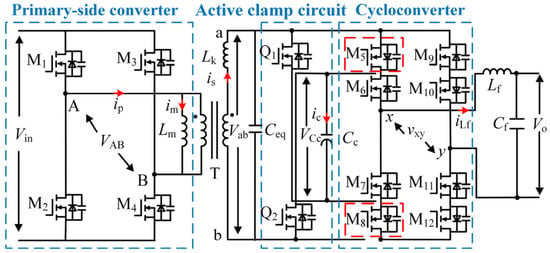
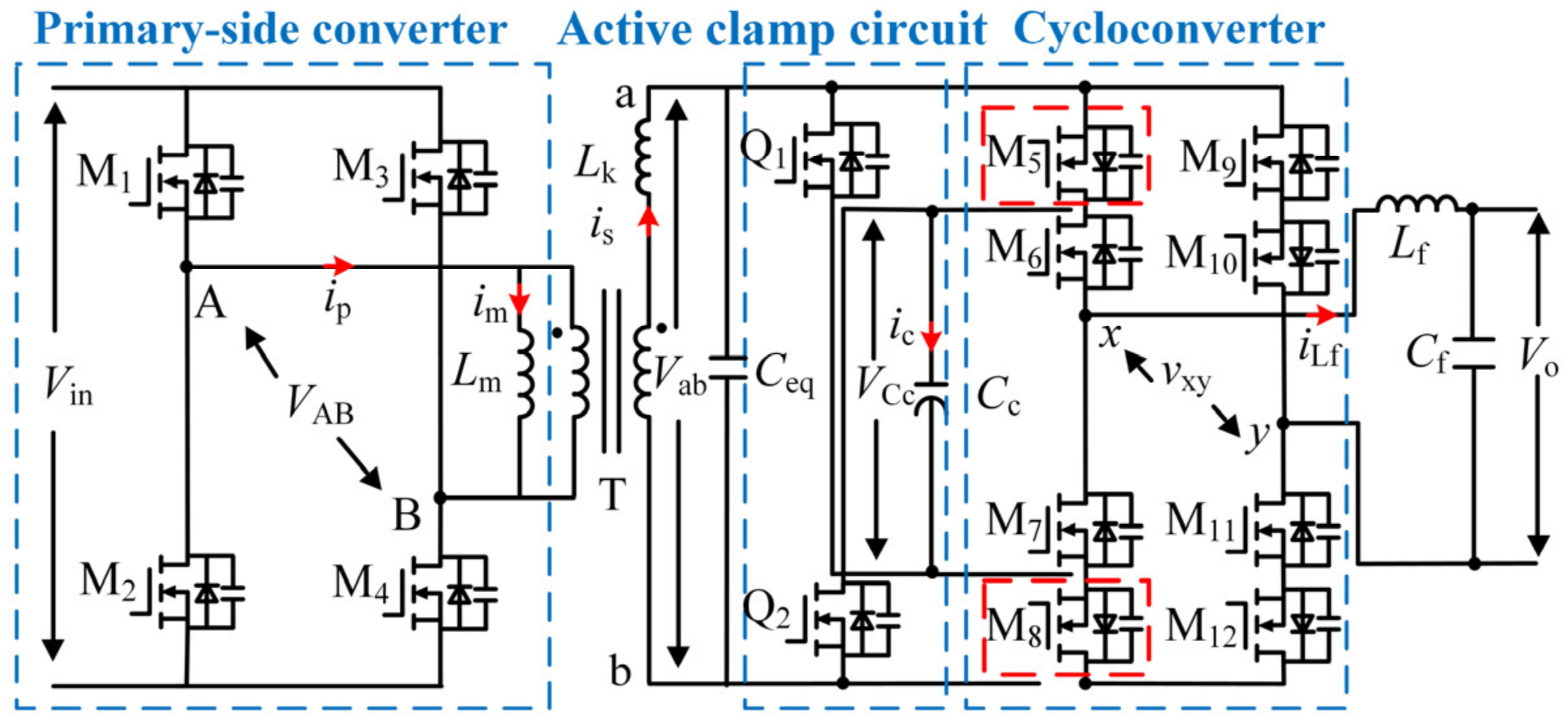
Although the aforementioned suppression circuits can mitigate voltage ringing to some extent, their effectiveness is limited, and none of them can suppress it to a level close to the steady-state voltage. The full-bridge active clamp circuit [19] can effectively suppress voltage ringing to the steady-state voltage, and its control strategy is simple and easy to implement; however, it requires a relatively large number of switching devices. To reduce the number of switching devices, a half-bridge active clamp circuit [20] has been proposed in the literature. Although this circuit reduces the number of switching devices, the newly added switching devices must withstand twice the steady-state voltage. On this basis, ref. [21] integrates and simplifies the full-bridge clamp circuit with the cycloconverter, resulting in a novel active clamp circuit, as shown in Figure 1. This circuit consists of two switching devices (Q1 and Q2) and one clamp capacitor (Cc), and can clamp the secondary-side voltage to the steady-state level. Compared with a cycloconverter-type inverter, this circuit increases the number of switching devices and enlarges the overall converter volume. However, its conventional modulation strategy for suppressing voltage ringing under non-unity power factor loads has not been sufficiently investigated.
Figure 1.
ACHFLI topology.
To address this issue, this paper proposes a modulation strategy that not only effectively suppresses voltage ringing but also improves the waveform distortion in the output voltage and current when their polarities are opposite. Compared with the conventional modulation strategy, the advantages of the proposed modulation strategy are as follows:
(1) Two MOSFETs on the secondary side achieve ZCS turn-off, and two MOSFETs operate entirely at low frequency within one line cycle, effectively reducing switching losses.
(2) The resonance between the secondary-side equivalent parasitic capacitance (Ceq) and the leakage inductance (Lk) is utilized to feed energy back to the primary side, thereby maintaining the stability of the clamp capacitor voltage, effectively suppressing voltage ringing, and improving the waveform distortion in the output voltage and current when their polarities are opposite.
The paper is organized as follows: Section 2 presents the principles of the proposed modulation strategy. Section 3 designs the clamp capacitor capacitance parameters. Section 4 validates the advantages of the proposed modulation strategy through experimental and simulation results. Finally, Section 5 concludes this paper.
2. Principle of Operation
2.1. Proposed Modulation Methods
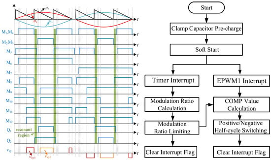
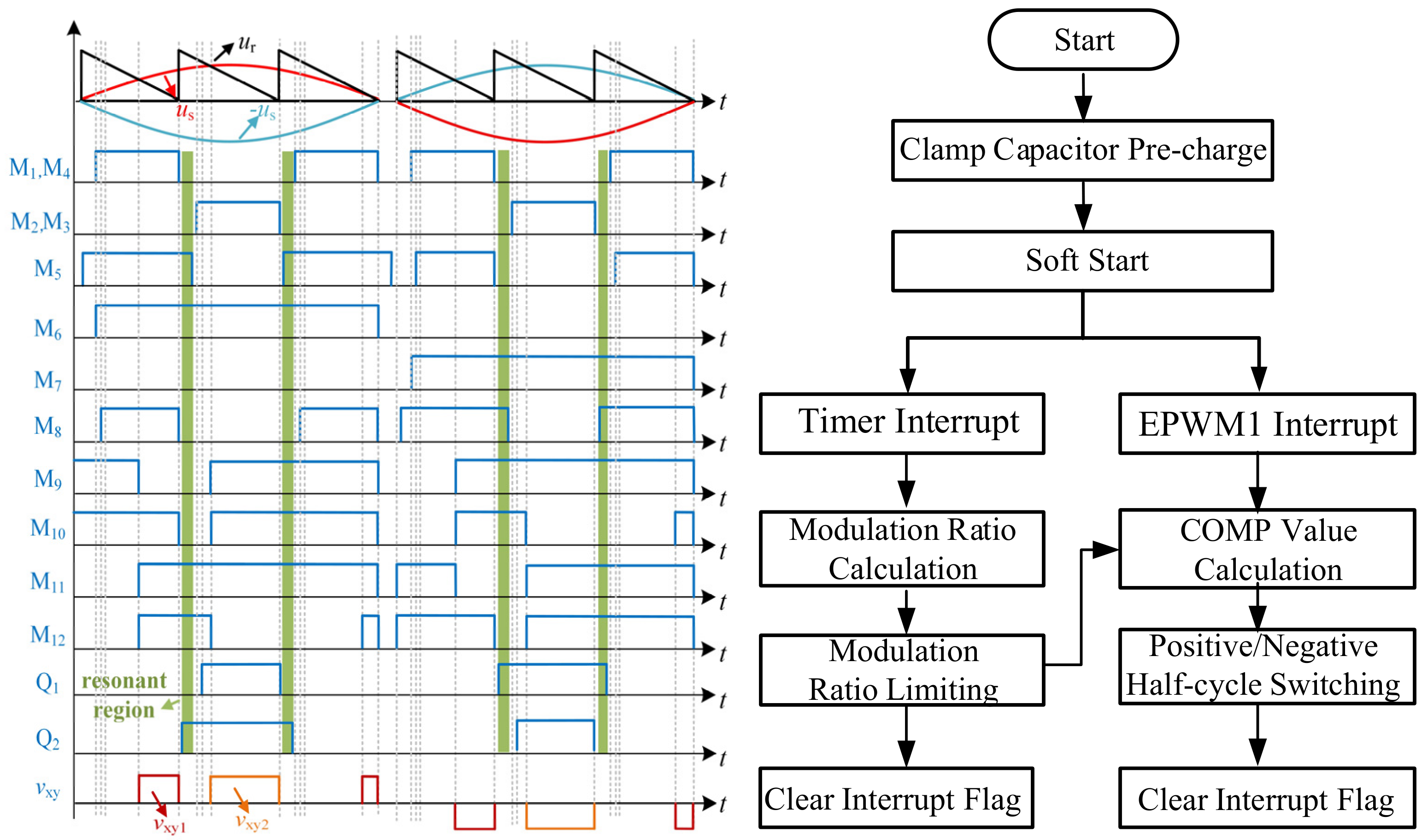
The proposed modulation strategy is shown in Figure 2. In this strategy, us represents the modulating wave, and ur represents the carrier wave. The primary-side MOSFETs operate at a fixed 50% duty cycle at the switching frequency fk. Within one switching cycle, two modulated pulses labeled vxy are generated (including vxy1 and vxy2), which increase the harmonic frequency without increasing switching losses, thereby reducing the filter requirement.
Figure 2.
Modulation strategy and flowchart for non-unity power factor loads.
The specific switching sequence is as follows: M1, M2, M3 and M4 operate with a constant 50% duty cycle, where M1 and M4 turn on simultaneously, and M2 and M3 turn on simultaneously. During the positive half-cycle of the line frequency, M6 and M7 operate at low frequency, with M6 remaining on and M7 remaining off; M8 turns on with a delay relative to M1 and M4, and its turn off is synchronized with that of M1 and M4; Q1 turns on with a delay relative to M2 and M3, and its turn-off is synchronized with that of M2 and M3; M5 and Q2 turn-on early during the dead time and turn-off with a delay, creating a resonant interval. To avoid short-circuiting the clamp capacitor, the switching sequence must satisfy the following conditions: when M5 turns on, Q1 is completely off; when M5 turns off, Q1 has not yet turned on; when Q2 turns on, M8 is completely off; when Q2 turns off, M8 has not yet turned on. The turn-on instant of M9 coincides with that of vxy2, and the turn-off instant of M9 coincides with that of vxy1; the turn on instant of M10 coincides with that of vxy2, and the turn-off instant of M10 is synchronized with that of M1 and M4; the turn-on instant of M11 coincides with that of vxy1, and the turn-off instant of M11 is synchronized with that of M1 and M4; M12 turns on with a delay relative to M1 and M4, and its turn-off instant coincides with that of vxy2.
During the negative half-cycle of the line frequency, M6 and M7 operate at low frequency, with M7 remaining on and M6 remaining off. M5 turns on with a delay relative to M1 and M4, and its turn-off is synchronized with that of M1 and M4. Q2 turns on with a delay relative to M2 and M3, and its turn-off is synchronized with that of M2 and M3. M8 and Q1 turn on early during the dead time and turn off with a delay, creating a resonant interval. To avoid short-circuiting the clamp capacitor, the switching sequence must satisfy the following conditions: when M8 turns on, Q2 is completely off; when M8 turns off, Q2 has not yet turned on; when Q1 turns on, M5 is completely off; when Q1 turns off, M5 has not yet turned on. The turn-on instant of M9 coincides with that of vxy1, and the turn-off instant of M9 is synchronized with that of M1 and M4. M10 turns on with a delay relative to M1 and M4, and its turn-off instant coincides with that of vxy2. The turn-on instant of M11 coincides with that of vxy2, and its turn-off instant coincides with that of vxy1. The turn-on instant of M12 coincides with that of vxy2, and its turn-off instant is synchronized with that of M1 and M4.
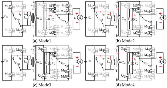
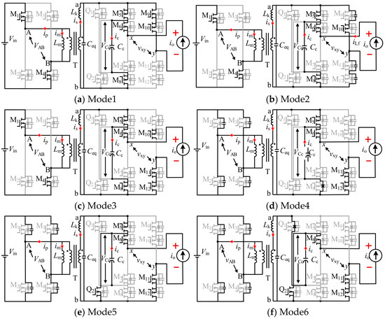
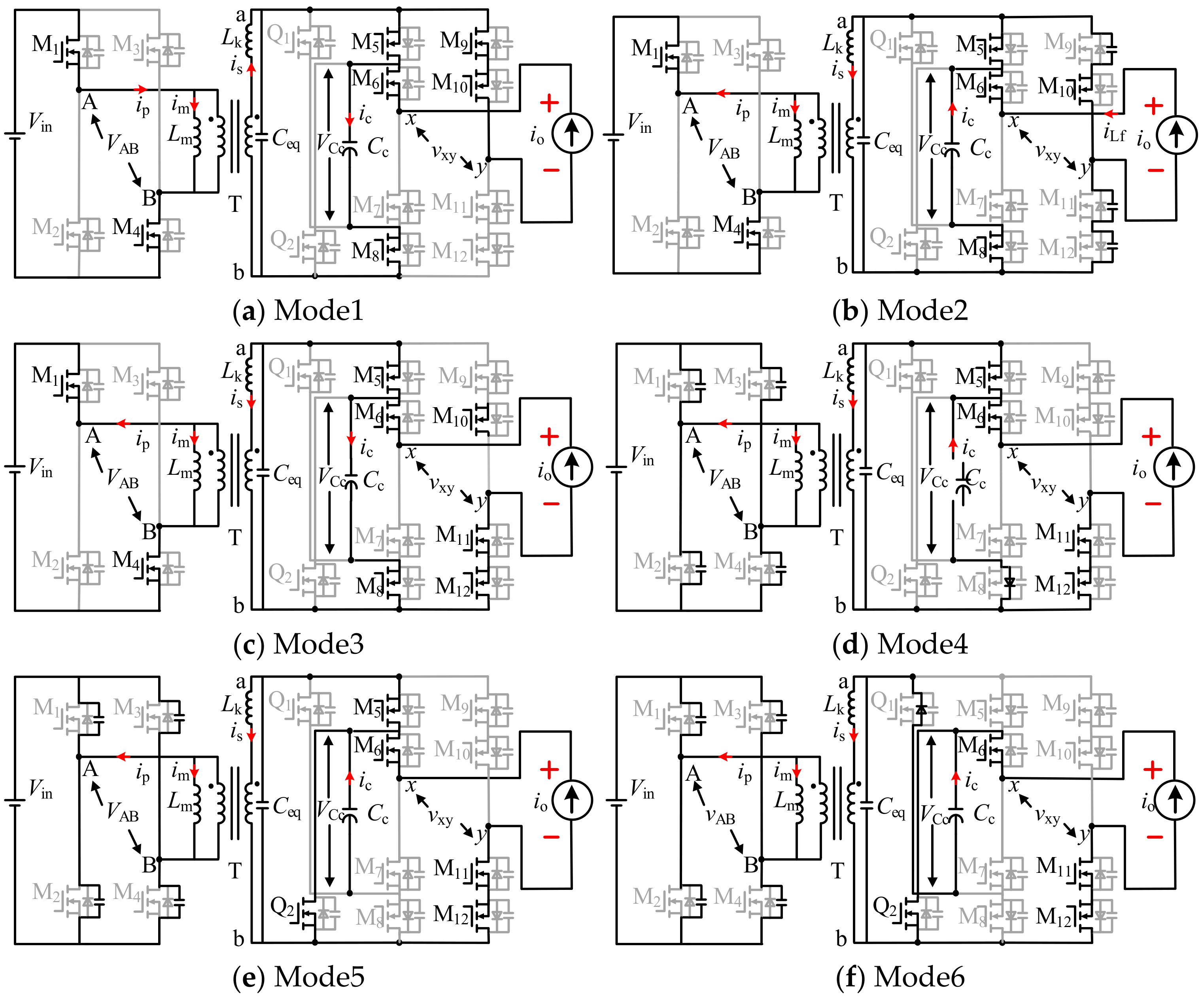
The simplified operating modes of the proposed modulation strategy in the region where the voltage and current have the same polarity (Vo > 0, io > 0) are shown in Figure 3.
Figure 3.
Simplified operating modes (Vo > 0, io > 0).
Mode 1: The circuit operates in a freewheeling state. The output current io flows through the loop formed by M5, M6, M9 and M10. Cc absorbs leakage inductance energy through M5 and M8.
Mode 2: Energy is transferred from the primary-side to the secondary-side load. The io flows through the loop formed by M5, M6, M11 and M12. Cc releases energy to the load through the path formed by M6, M8, M11 and M12.
Mode 3: The circuit enters the freewheeling state again. The io flows through the loop formed by M6, M11, M12, and Q2. Cc absorbs leakage inductance energy through Q1 and Q2. During this period, M10 is turned off. Since there is no current flowing through its branch, M10 achieves ZCS turn-off.
Mode 4: Energy is transferred from the primary-side to the secondary-side load again. The io flows through the loop formed by M6, M9, M10, and Q2. Cc absorbs leakage inductance energy through Q1 and Q2. M11 is turned off during Mode 1. Since there is no current flowing through its branch at turn-off, M11 achieves ZCS turn-off.
From the above analysis, it can be seen that the clamp capacitor absorbs leakage inductance energy during the freewheeling mode and then releases this energy to the load during the energy transfer mode, thereby ensuring that the clamp capacitor voltage remains in a charge-balanced state.
2.2. Operating Mode
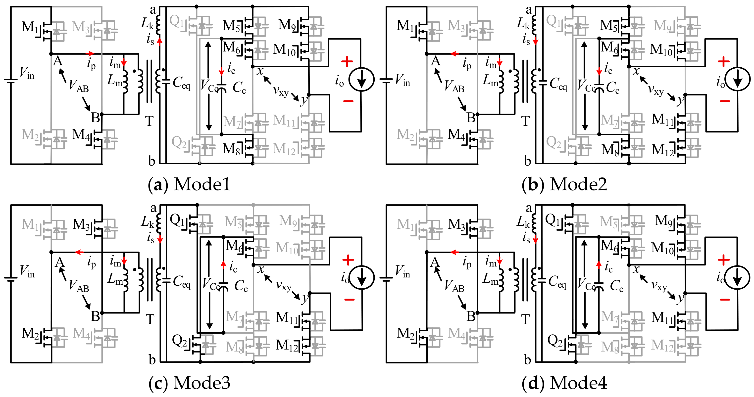
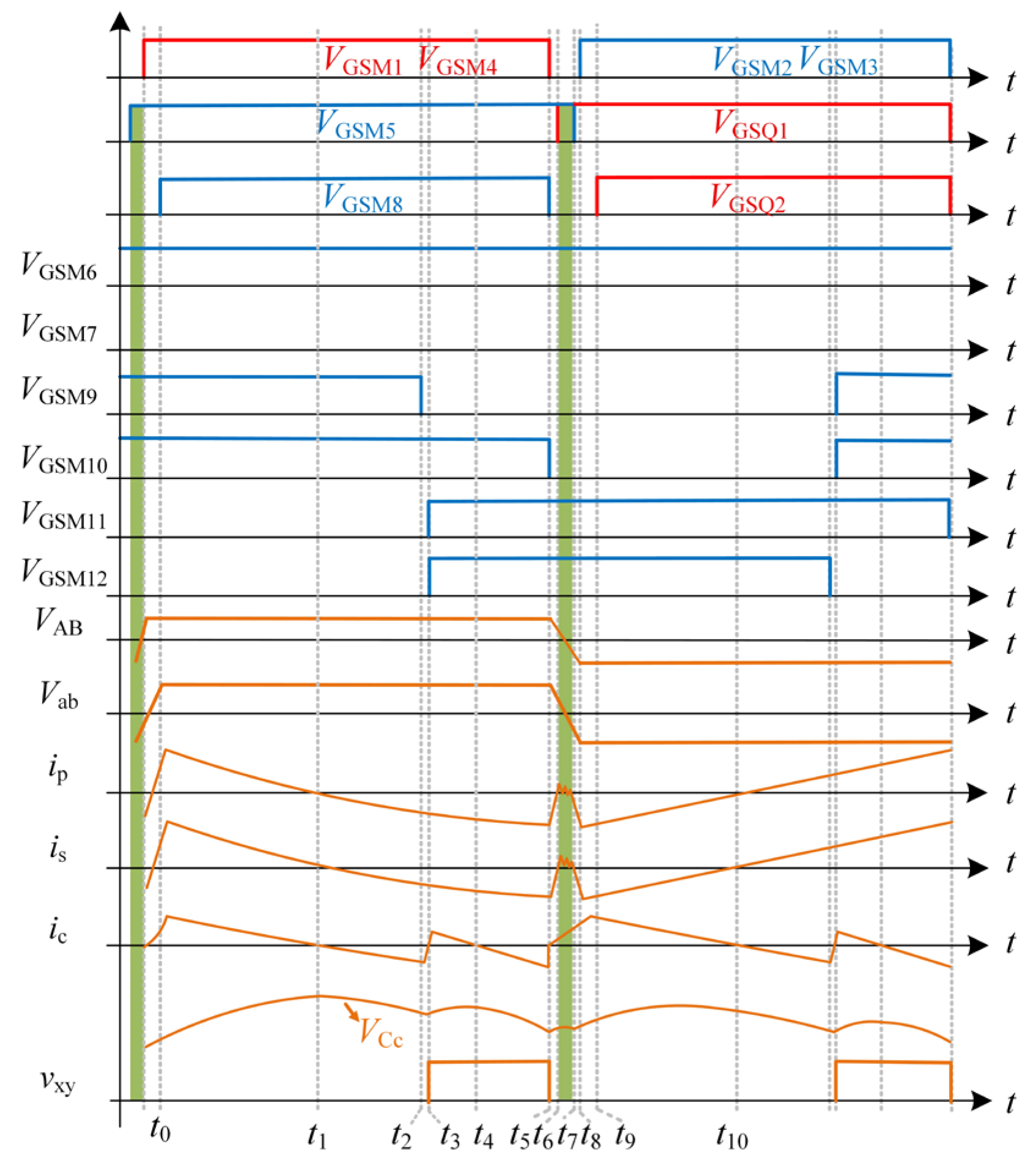
In practical applications, non-unity power factor loads (mainly resistive–inductive and resistive–capacitive loads) introduce a phase shift between the output voltage and current of the inverter, resulting in intervals where the voltage and current have opposite polarities (Vo > 0, io < 0 and Vo < 0, io > 0). In this paper, the interval where the output voltage and current are in opposite polarities (Vo > 0, io < 0) is taken as an example to analyze in detail the operating modes within one switching cycle. Figure 4 shows the key waveforms of the active-clamped high-frequency-link inverter during a single switching cycle, and Figure 5 shows the corresponding circuit states of the operating modes. To simplify the analysis, the following assumptions are made:
Figure 4.
Waveforms of the ACHFLI within a single switching cycle (Green: overlap between VGSM5 and VGSQ1).
Figure 5.
Operating modes of the ACHFLI within a single switching cycle.
(1) The transformer and all MOSFETs are assumed to be ideal devices.
(2) The output capacitances of the primary-side MOSFETs are denoted as CPN (N = 1–4), and those of the secondary-side MOSFETs are denoted as CSM (M = 5–12) and CQX (X = 1, 2).
(3) The output capacitances of the primary-side MOSFETs are assumed to be equal, denoted as CP; similarly, the output capacitances of the secondary-side MOSFETs are assumed to be equal, denoted as CS.
Mode 1 (t0–t2): The circuit operates in a freewheeling state. The io flows through the loop formed by M5, M6, M9, and M10. During the interval t0–t1, Cc absorbs leakage inductance energy through M5 and M8. During t1–t2, since the clamp voltage is higher than the steady-state voltage nVin, the Cc releases energy to the primary side.
Mode 2 (t2–t3): M9 turns off, and io transfers from the loop formed by M5, M6, CS9, and M10 to the loop formed by M5, M6, CS11, and CS12. During this process, io charges CS9 and discharges CS11. At the end of this mode, CS11 is discharged to zero.
Mode 3 (t3–t5): M11 achieves ZVS turn-on, and io releases energy to the primary side through the loop formed by M5, M6, M11, and M12. During the interval t3–t4, the Cc absorbs secondary-side energy through M6 and M8, and the clamp capacitor voltage rises. During t4–t5, the Cc releases energy to the primary side through M5 and M8, and the clamp capacitor voltage falls.
Mode 4 (t5–t6): Primary-side switches M1 and M4 turn-off. M10 turns off; since there is no current flowing through its branch, M10 achieves ZCS turn-off. io releases energy to the primary side through the loop formed by M5, M6, M11, and M12.
Mode 5 (t6–t7): Q2 turns on early. Lk and Ceq resonate, feeding energy back to the primary side. io transfers from the loop formed by M5, M6, M11, and M12 to the loop formed by Q2, M6, M11, and M12.
Mode 6 (t7–t8): io flows through the loop formed by Q2, M6, M11, and M12. When CQ1 is discharged to zero, the leakage inductance energy is absorbed by Cc through the body diode of Q1 and Q2, and the clamp capacitor voltage rises.
The operating modes in the second half of the high-frequency switching cycle are symmetric to those analyzed above and are not described here for brevity. Under non-unity power factor load conditions, voltage ringing becomes more severe. By introducing a resonant path formed by Lk and Ceq to feed energy back to the primary side, the clamp capacitor voltage can be effectively maintained stable, thereby improving the distortion in the output voltage waveform. During the positive half-cycle of the line frequency, M10 and M11 are not in the current path when they turn off, thus achieving ZCS turn-off. Similarly, during the negative half-cycle of the line frequency, M9 and M12 can also achieve ZCS turn-off.
3. Design of the Clamp Capacitor
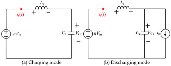
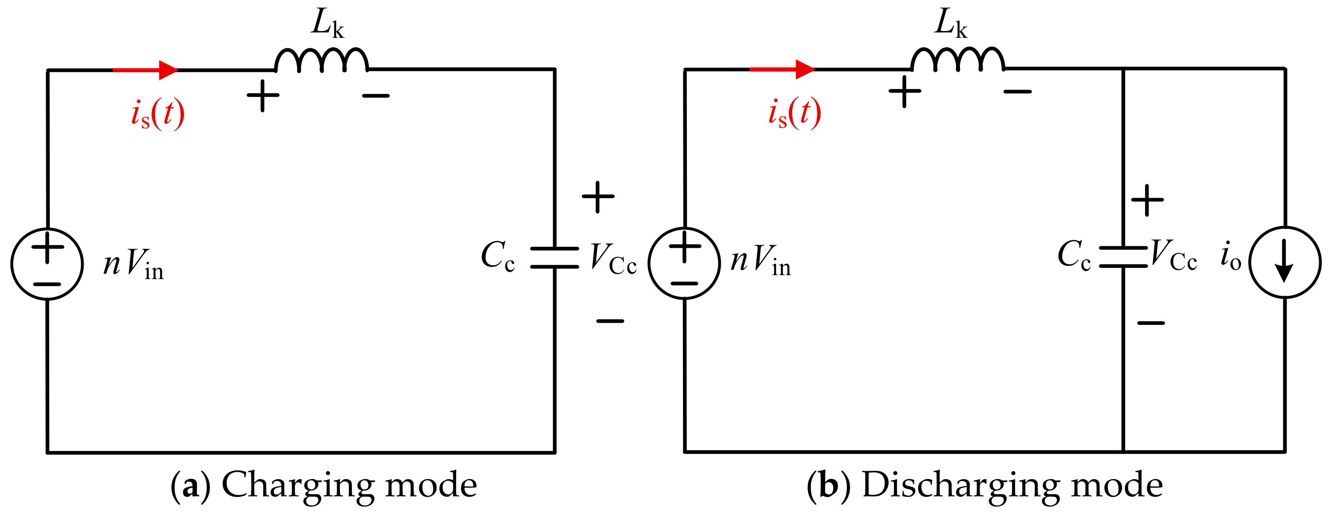
Based on the analysis of the charging and discharging states of the clamp capacitor, the corresponding equivalent circuit model is shown in Figure 6.
Figure 6.
Clamp Capacitor Charging and Discharging Equivalent Circuit Mode.
According to the circuit model of the CC charging state, the equation can be formulated as follows.
Assuming is(0) = Is and VCc(0) = VC, solving the above equations yields
To simplify the calculation, it is assumed that io remains constant at Io within one switching cycle. Then, according to the circuit model of the Cc-discharging state, the equation can be formulated as follows.
The initial state of the circuit is
Let D be the duty cycle, Is1 the initial condition of the secondary current, and VC1 the initial condition of the clamp capacitor voltage. Substituting these into Equation (3) and solving yields
To ensure the stability of the clamp capacitor voltage, its voltage ripple amplitude must not exceed 5% of the steady-state voltage nVin.
Using the relevant experimental parameters (specific parameters are given in Section 4), substituting Lk = 12.9 μH, Io = 2.73 A, n = 5, Is1 = 2.73 A and Vin = 40 V into Equation (6) yields a minimum clamp capacitance of 3.8 μF. To ensure the stability of the clamp capacitor voltage, a clamp capacitance of 15 μF is selected in this paper.
4. Simulation and Experimental Results
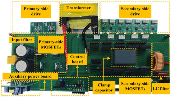
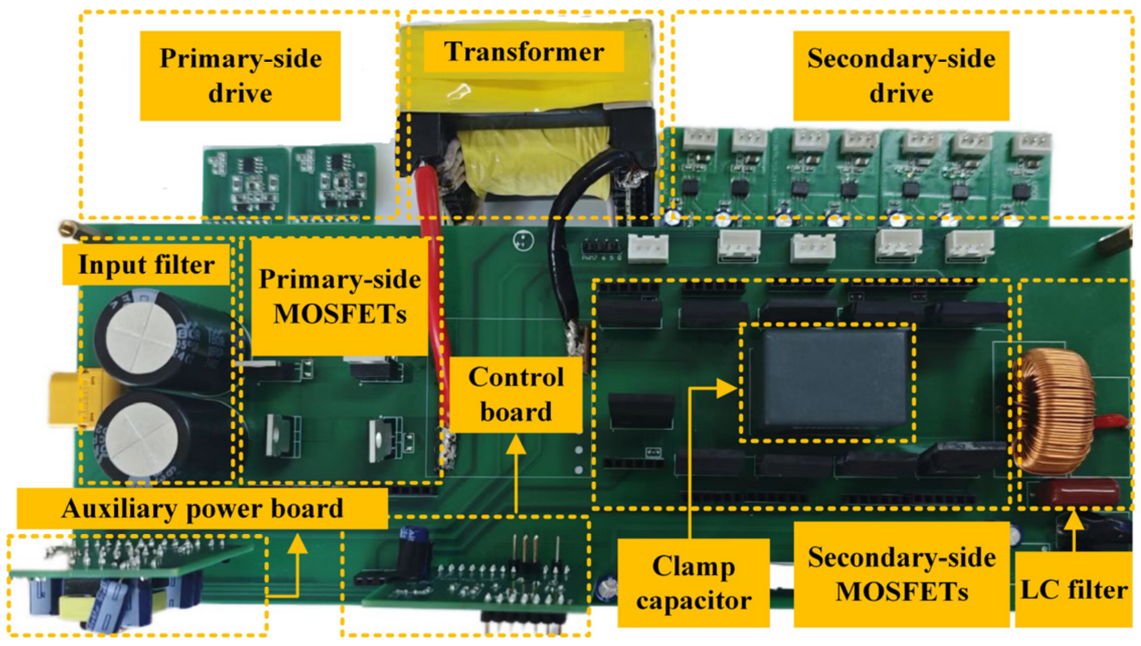
To verify the proposed modulation strategy, a 300 W prototype with 48 Vin input and 110 Vo output is built (see Figure 7). The key parameters and components are listed in Table 1. Although a 300 W prototype is demonstrated here, the proposed modulation strategy can be readily scaled to higher power levels (well beyond 300 W, e.g., several kilowatts) by resizing the power devices and magnetic components accordingly. Moreover, the strategy does not rely on a specific transformer turns ratio; it can be easily adapted to other input/output voltage specifications by adjusting the control parameters.
Figure 7.
Experimental prototype.
Table 1.
Specifications of the inverter prototype.
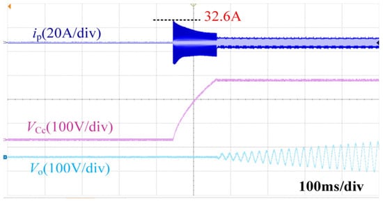
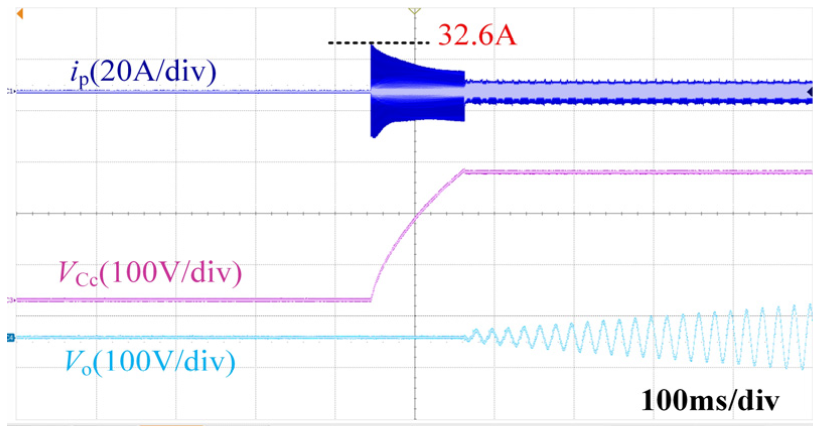
To avoid excessive inrush current on the primary side when charging the Cc, the primary-side MOSFETs operate with a small duty cycle to pre-charge the Cc, as shown in Figure 8. Once the clamp capacitor voltage reaches nVin, the secondary side initiates a soft start and eventually transitions to normal operation. With pre-charging, the maximum inrush current is only 32.6 A.
Figure 8.
Pre-charge waveforms of the clamp capacitor.
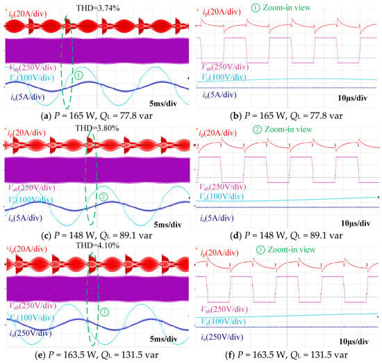
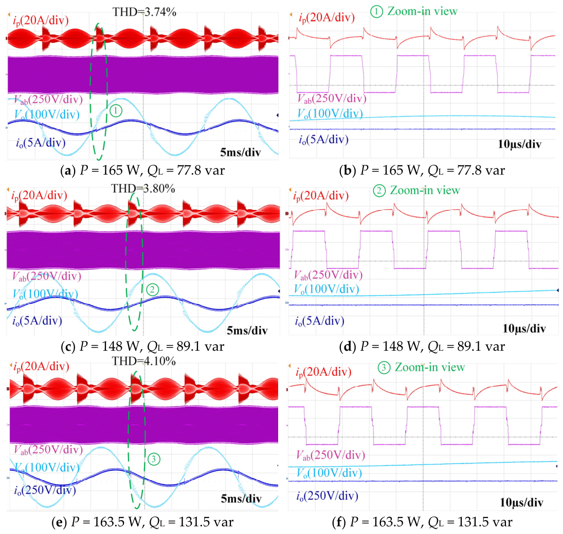
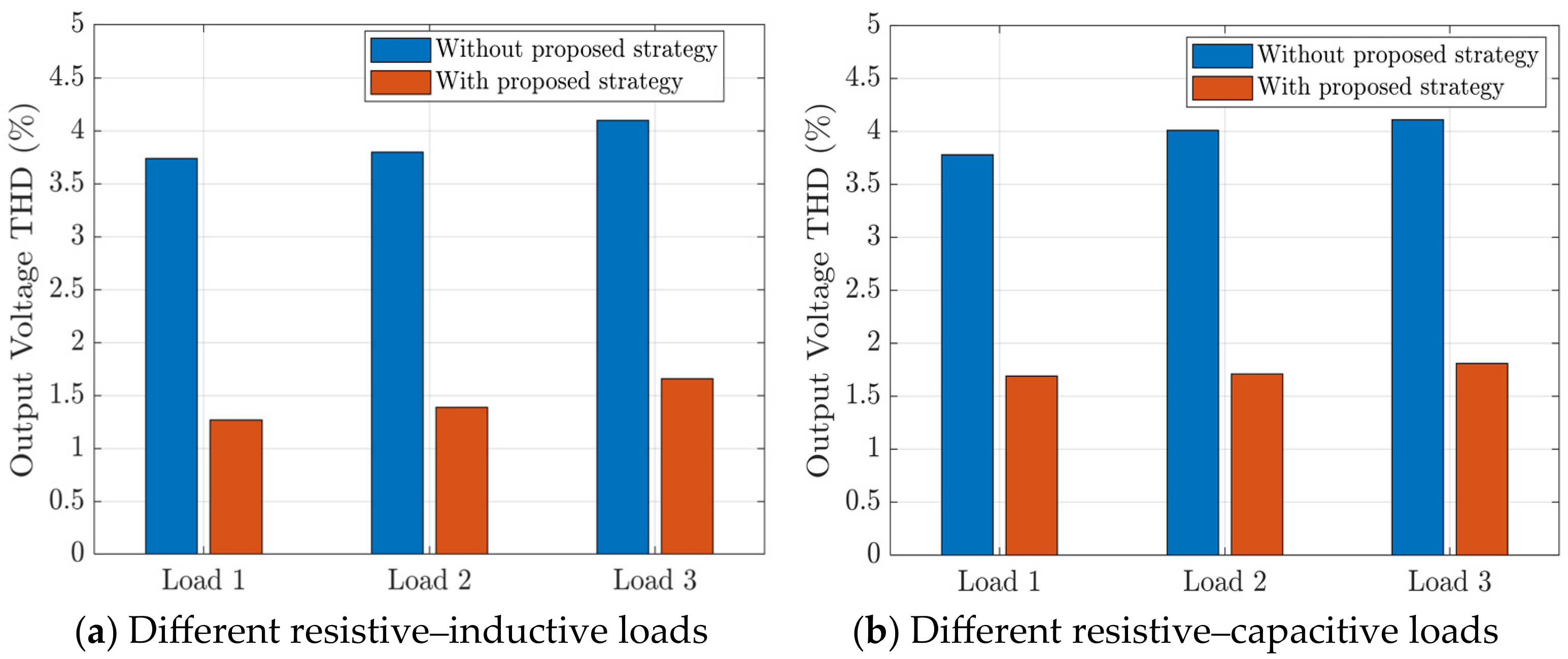
Figure 9 shows the experimental waveforms of the primary-side current ip, secondary-side voltage Vab, output voltage Vo, and output current io without the proposed improved modulation strategy (without introducing the Lk and Ceq resonant region) under three different resistive–inductive load conditions: (1) P = 165 W, QL = 77.8 var; (2) P = 148 W, QL = 89.1 var; (3) P = 163.5 W, QL = 131.5 var (P: active power; QL: inductive reactive power). During the intervals when the output voltage and output current have opposite polarities, severe waveform distortion is observed, with the output voltage THD reaching 3.74%, 3.8%, and 4.1%, respectively. Meanwhile, the ip increases significantly during these intervals.
Figure 9.
Waveforms of ip, Vab, Vo, and io under different resistive–inductive loads without the proposed improved modulation strategy (Vin = 48 V).
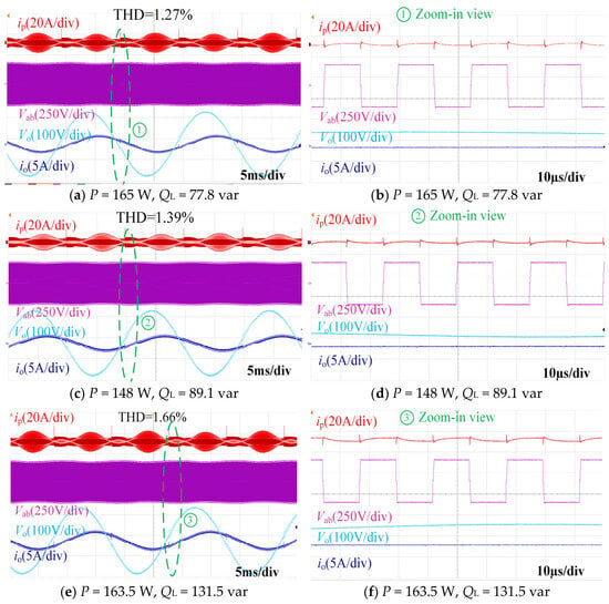
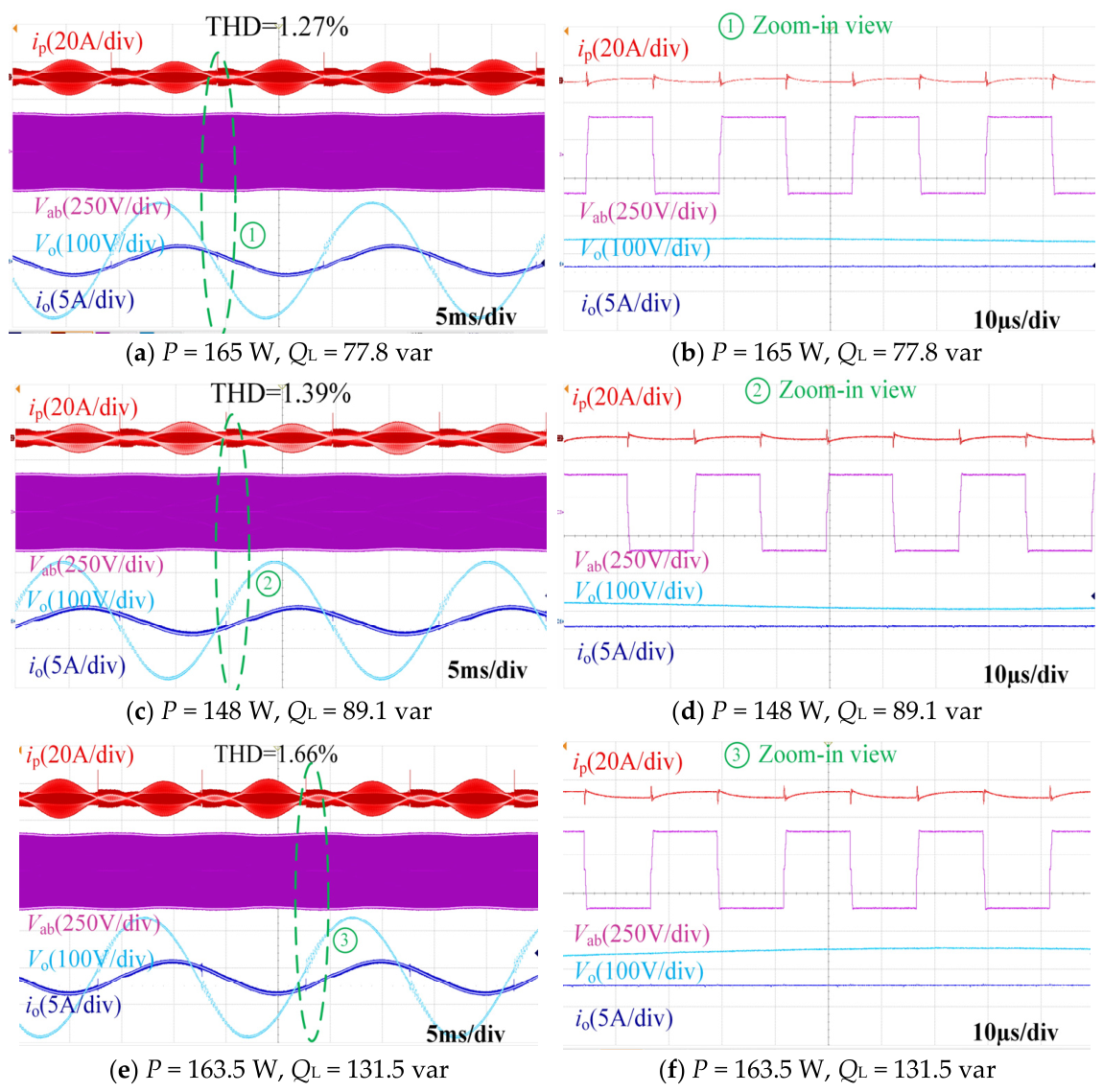
Figure 10 shows the experimental waveforms of the ip, Vab, Vo, and io under the same resistive–inductive load conditions (identical to the three load cases in Figure 9) with the proposed improved modulation strategy (by introducing the Lk and Ceq resonant region). During the intervals when the output voltage and output current have opposite polarities, the waveform distortion is significantly mitigated, and the output voltage THD is reduced to 1.27%, 1.39%, and 1.66%, respectively. Moreover, ip does not exhibit a significant increase during these intervals, and its variation trend remains consistent with that of io. In addition, it can be observed from the figure that the secondary-side voltage approaches the steady-state value and the voltage ringing is effectively suppressed.
Figure 10.
Waveforms of ip, Vab, Vo, and io under different resistive–inductive loads with the proposed improved modulation strategy (Vin = 48 V).
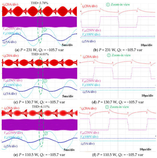
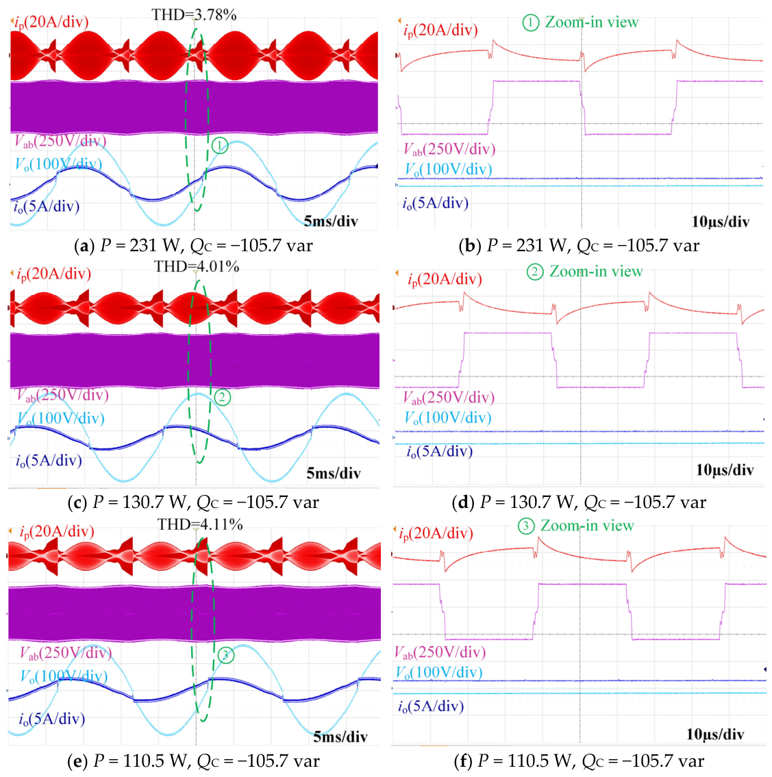
Figure 11 shows the experimental waveforms of ip, Vab, Vo, and io without the proposed improved modulation strategy (without introducing the Lk and Ceq resonant region) under different resistive–capacitive load conditions. The three load cases are: (1) P = 231 W, QC = −105.7 var; (2) P = 130.7 W, QC = −105.7 var; (3) P = 110.5 W, QC = −105.7 var (QC: capacitive reactive power.). During the intervals when the output voltage and output current have opposite polarities, severe waveform distortion is observed, with the output voltage THD reaching 3.78%, 4.01%, and 4.11%, respectively. Meanwhile, the ip increases significantly during these intervals.
Figure 11.
Waveforms of ip, Vab, Vo, and io under different resistive–capacitive loads without the proposed improved modulation strategy (Vin = 48 V).
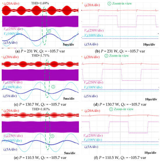
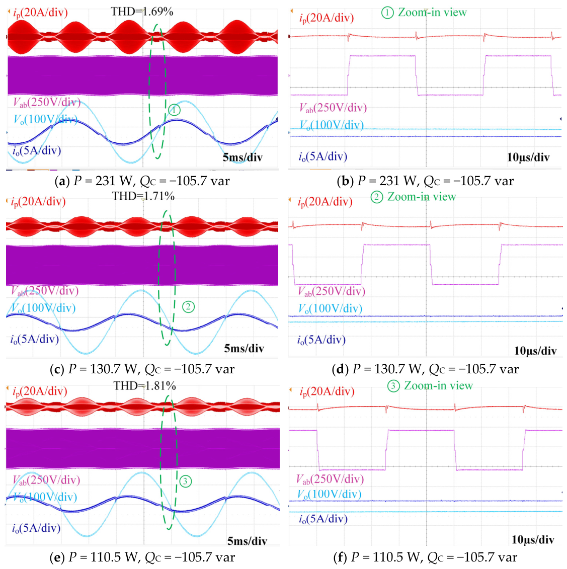
Figure 12 presents the experimental waveforms of the ip, Vab, Vo, and io under the same resistive–inductive load conditions (identical to the three load cases in Figure 11) with the proposed improved modulation strategy (by introducing the Lk and Ceq resonant region). During intervals when the output voltage and output current have opposite polarities, the waveform distortion is significantly mitigated, and the output voltage THD is reduced to 1.69%, 1.71%, and 1.81%, respectively. Moreover, ip does not exhibit a significant increase during these intervals, and its variation trend remains consistent with that of io. In addition, it can be observed from the figure that the secondary-side voltage approaches the steady-state value and the voltage ringing is effectively suppressed.
Figure 12.
Waveforms of ip, Vab, Vo, and io under different resistive–capacitive loads with the proposed improved modulation strategy (Vin = 48 V).
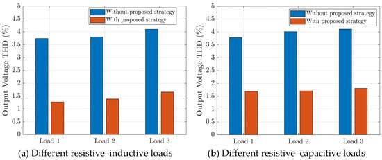
Figure 13 compares the output voltage THD of the two modulation strategies under resistive–capacitive and resistive–inductive loads. By introducing the resonant region, the proposed modulation strategy can feed energy back to the primary side, thereby better maintaining the voltage stability of the clamp capacitor under non-unity-power-factor loads (mainly including resistive–capacitive and resistive–inductive loads). Consequently, this strategy effectively mitigates the waveform distortion during intervals when the output voltage and output current have opposite polarities, reducing the output voltage THD by up to 2.74%.
Figure 13.
THD comparison of two modulation strategies under resistive–inductive and resistive–capacitive loads.
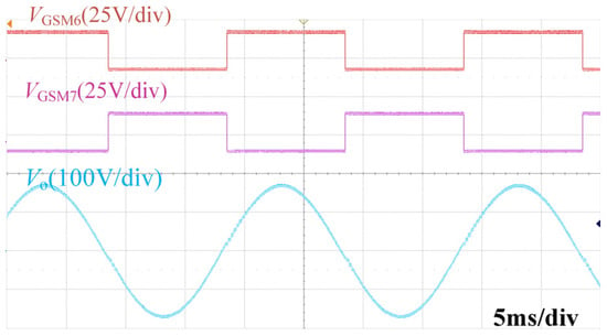
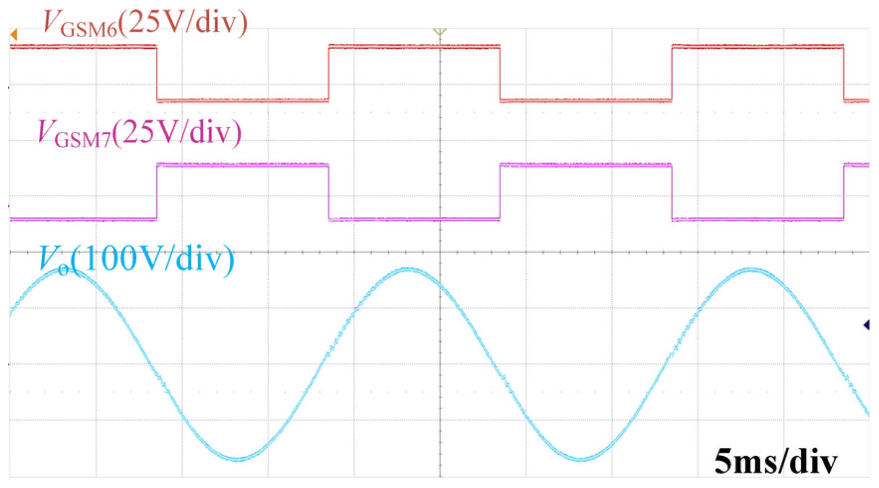
Figure 14 shows the experimental waveforms of the gate drive voltages VGSM6 (M6), VGSM7 (M7), and the output voltage Vo. It can be observed that the switching frequencies of M6 and M7 are identical to the output voltage frequency, indicating that both switches operate in a low-frequency regime.
Figure 14.
Waveforms of the gate drive voltages VGSM6, VGSM7, and Vo.
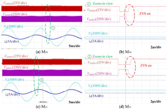
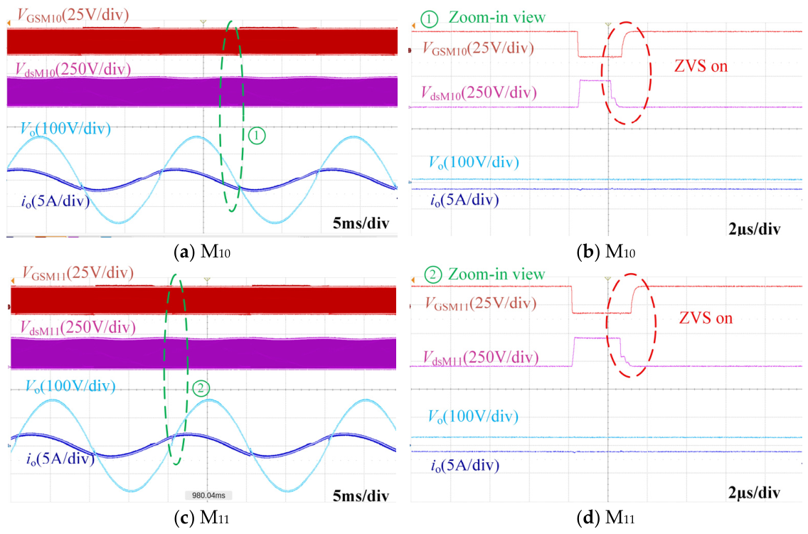
Figure 15 shows the gate-source drive voltage VGS and drain-source voltage Vds of the secondary-side switches. It can be observed that VGS starts to rise only when Vds is zero, with no overlap between them, indicating that M10 and M11 achieve ZVS turn-on.
Figure 15.
Soft-switching waveforms of M10 and M11 (Vo > 0, io < 0).
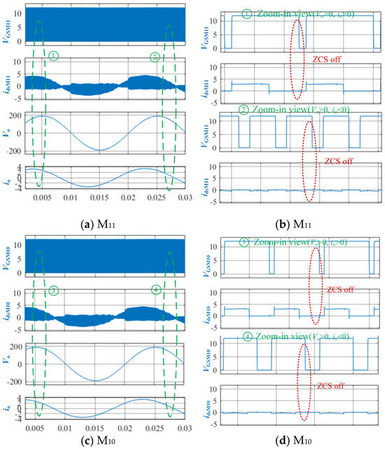
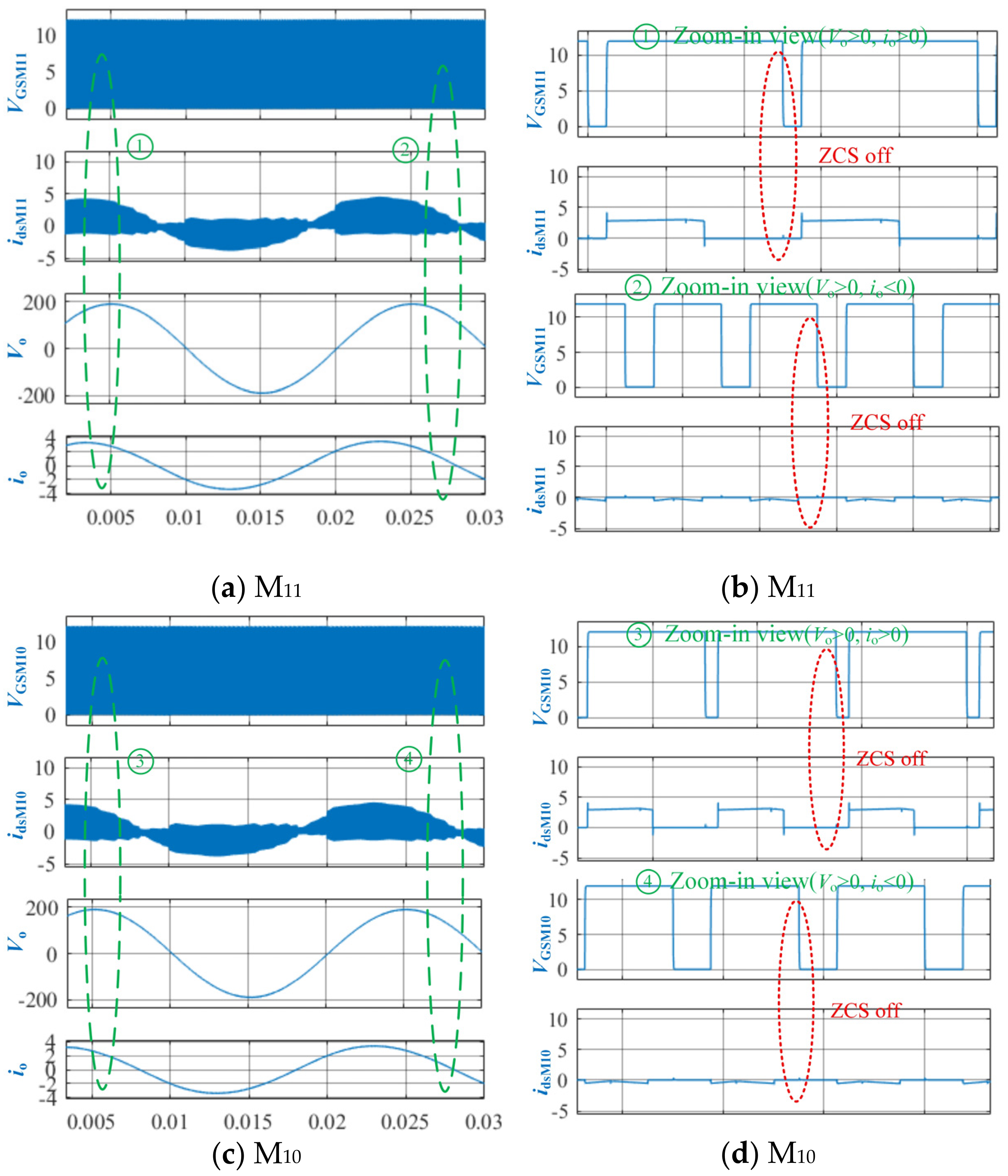
Figure 16 shows the simulated waveforms of the gate-source drive voltage VGS of M10 and M11 and the drain-source current ids. It can be observed that ids is zero when M10 and M11 are turned off, indicating that both switches achieve ZCS turn-off. Under the same experimental conditions, the conduction losses and transformer losses of the proposed modulation strategy and the modulation strategy in [21] are essentially equivalent, and both can achieve soft switching of the primary-side MOSFETs. Therefore, the comparison focuses on the switching losses caused by the secondary-side MOSFETs, which can be expressed as:
Figure 16.
Soft-switching waveforms of M10 and M11 (Vo > 0, io < 0/Vo > 0, io > 0).
Substituting Vds = 240 V, Ids-on = 4.925 A, Ids-off = 3.325 A, ton = 88 ns, toff = 57 ns, and fk = 40 kHz/50 Hz into Equation (7) yields that the switching loss of the proposed modulation strategy is reduced by approximately 5.7 W compared with that of the modulation strategy in [21].
5. Conclusions
This paper addresses aggravated voltage ringing and severe distortion in the output voltage and current waveforms of ACHFLI under non-unity power factor loads, and proposes an improved modulation strategy with leakage energy feedback. In this strategy, two secondary-side MOSFETs achieve ZCS turn-off, while the other two MOSFETs operate at low frequency throughout the entire line cycle. By feeding the leakage inductance energy back to the primary side, the voltage balance of the clamping capacitor is effectively maintained, thereby significantly mitigating the waveform distortion in the output voltage and current during intervals when their polarities are opposite. Experimental results demonstrate that the proposed modulation strategy effectively alleviates the waveform distortion when the voltage and current have opposite polarities, and the THD of the output voltage is reduced by a maximum of 2.74%, confirming the feasibility and effectiveness of the approach.
Author Contributions
Conceptualization, B.G. and F.M.; methodology, B.G. and F.M.; software, W.G., H.G., C.Y. and Z.L. (Zhipeng Liu); validation, X.L. and M.Z.; formal analysis, Y.H. and Y.D.; investigation, P.Z.; data curation, Z.L. (Zhiyang Liu) and J.Z.; writing—original draft preparation, B.G., S.R. and P.Z.; writing—review and editing, H.C. and R.Z.; visualization, S.R. and W.G.; supervision, B.G. and F.M. All authors have read and agreed to the published version of the manuscript.
Funding
State Grid Corporation of China Technology Project, 522437260001.
Data Availability Statement
The original contributions presented in this study are included in the article. Further inquiries can be directed to the corresponding author.
Conflicts of Interest
The authors declare no conflicts of interest. Author B.G., S.R., W.G., H.G., C.Y., Z.L. (Zhipeng Liu), X.L., M.Z., Y.H., Y.D., Z.L. (Zhiyang Liu), J.Z., H.C. and R.Z. was employed by the company State Grid Heilongjiang Electric Power Research Institute, Harbin, China. The remaining authors declare that the research was conducted in the absence of any commercial or financial relationships that could be construed as a potential conflict of interest.
Abbreviations
The following abbreviations are used in this manuscript:
| HFLI | High-Frequency Link Inverters |
| ACHFLI | Active-Clamped High-Frequency Link Inverters |
| ZCS | Zero-Current Switching |
| THD | Total Harmonic Distortion |
| ZVS | Zero-Voltage Switching |
References
- Guo, X.; Zhang, L.; Wei, Y.; Wu, S. A coordination control method for current stress reduction in high-frequency link matrix converter. IEEE Trans. Ind. Electron. 2023, 71, 9972–9981. [Google Scholar] [CrossRef] [Scilit]
- Basu, K.; Mohan, N. A high-frequency link single-stage PWM inverter with common-mode voltage suppression and source-based commutation of leakage energy. IEEE Trans. Power Electron. 2013, 29, 3907–3918. [Google Scholar]
- Chambayil, A.; Chattopadhyay, S. A dual active bridge converter with multiphase boost interfaces for single-stage bidirectional DC-AC conversion. IEEE Trans. Ind. Appl. 2021, 57, 2638–2653. [Google Scholar] [CrossRef] [Scilit]
- Jin, P.; Hu, Y.; Lei, G.; Guo, Y.; Zhu, J. A novel SVM strategy to reduce current stress of high-frequency link matrix converter. IEEE Trans. Ind. Electron. 2023, 71, 4652–4662. [Google Scholar] [CrossRef] [Scilit]
- Yang, Q.; Yang, J.; Li, R. Analysis of grid current distortion and waveform improvement methods of dual-active-bridge microinverter. IEEE Trans. Power Electron. 2023, 38, 4345–4359. [Google Scholar]
- Li, X.; Liu, J.; Ji, F.; Cao, X.; Wang, Y.; Liu, J. A single-stage high frequency-link split-phase microinverter for both grid-tied and islanded operation. IEEE Trans. Power Electron. 2024, 39, 10409–10423. [Google Scholar] [CrossRef] [Scilit]
- Morsali, P.; Dey, S.; Mallik, A.; Akturk, A. Switching modulation optimization for efficiency maximization in a single-stage series resonant DAB-based DC-AC converter. IEEE J. Emerg. Sel. Top. Power Electron. 2023, 11, 5454–5469. [Google Scholar] [CrossRef] [Scilit]
- Wang, P.; Guo, D.; Hu, J.; Wang, W.; Xu, D. Natural power factor correction and soft switching design for a single-stage bidirectional dual active bridge AC–DC converter. IEEE Trans. Power Electron. 2024, 39, 5349–5360. [Google Scholar] [CrossRef] [Scilit]
- Li, X.; Liu, J.; Zhou, X.; Liu, J. A High-Frequency-Link Split-Phase Voltage-Source Microinverter Based on Buck–Boost AC Chopper for High Efficiency and Low Voltage Stress. IEEE Trans. Power Electron. 2025, 40, 11673–11689. [Google Scholar]
- Mazumder, S.K. Hybrid modulation scheme for a high-frequency AC-link inverter. IEEE Trans. Power Electron. 2016, 31, 861–870. [Google Scholar] [CrossRef] [Scilit]
- Zhou, X.; Xu, J.; Zhong, S. Single-stage soft-switching low-distortion bipolar PWM modulation high-frequency-link DC-AC converter with clamping circuits. IEEE Trans. Ind. Electron. 2018, 65, 7719–7729. [Google Scholar] [CrossRef] [Scilit]
- Wang, M.; Guo, S.; Huang, Q.; Yu, W.; Huang, A.Q. An isolated bidirectional single-stage DC-AC converter using wide-band-gap switches with a novel carrier-based unipolar modulation technique under synchronous rectification. IEEE Trans. Power Electron. 2017, 32, 1832–1843. [Google Scholar]
- Kummari, N.; Chattopadhyay, S. Three-legged high-gain phase-modulated DC-AC converter for mitigation of device capacitance induced ringing voltage. IEEE Trans. Power Electron. 2020, 35, 1306–1321. [Google Scholar] [CrossRef] [Scilit]
- Nayak, P.; Rajashekara, K.; Pramanick, S.K. Soft-switched modulation technique for a single-stage matrix-type isolated DC–AC converter. IEEE Trans. Ind. Appl. 2019, 55, 7642–7656. [Google Scholar] [CrossRef] [Scilit]
- Chen, D.; Chen, Y. Step-up AC voltage regulators with high-frequency link. IEEE Trans. Power Electron. 2013, 28, 390–397. [Google Scholar] [CrossRef] [Scilit]
- Wang, Y.; Liu, H.; Wheeler, P. Research on the voltage spike suppression strategy for three-phase high frequency link matrix-type inverter. IEEE J. Emerg. Sel. Top. Power Electron. 2022, 10, 6070–6083. [Google Scholar] [CrossRef] [Scilit]
- Blinov, A.; Verbytskyi, I.; Peftitsis, D.; Vinnikov, D. Regenerative passive snubber circuit for high-frequency link converters. IEEE J. Emerg. Sel. Top. Ind. Electron. 2022, 3, 252–257. [Google Scholar] [CrossRef] [Scilit]
- Maddipudi, R.; Chattopadhyay, S. Modulation strategy for bidirectional power flow on a high-frequency link AC-DC converter topology that mitigates the device voltage overshoot. IEEE Trans. Ind. Appl. 2024, 60, 4156–4167. [Google Scholar] [CrossRef] [Scilit]
- Xu, D.; Zhong, S.; Xu, J. Bipolar phase shift modulation single-stage audio amplifier employing a full bridge active clamp for high efficiency low distortion. IEEE Trans. Ind. Electron. 2021, 68, 1118–1129. [Google Scholar] [CrossRef] [Scilit]
- Zhong, S.; Xu, J.; Zhou, X. High-efficiency zero-voltage switching single-stage switching amplifier with half-bridge active clamping circuit. IEEE Trans. Ind. Electron. 2018, 65, 8574–8584. [Google Scholar] [CrossRef]
- Zhang, J.; Xu, Q.; Guo, P.; Mo, N.; Hu, J.; Tang, C. Multiplexed active clamp high-frequency link inverter with de–re-coupling frequency doubling modulation. IEEE Trans. Ind. Electron. 2023, 70, 5885–5895. [Google Scholar] [CrossRef] [Scilit]

Disclaimer/Publisher’s Note: The statements, opinions and data contained in all publications are solely those of the individual author(s) and contributor(s) and not of MDPI and/or the editor(s). MDPI and/or the editor(s) disclaim responsibility for any injury to people or property resulting from any ideas, methods, instructions or products referred to in the content. |
© 2026 by the authors. Licensee MDPI, Basel, Switzerland. This article is an open access article distributed under the terms and conditions of the Creative Commons Attribution (CC BY) license.