


Abstract
The critical current (Ic) of a Josephson junction (JJ) is a significant physical parameter that plays a crucial role in the design of subsequent devices and circuits, as well as in the optimization of manufacturing processes. To ensure accurate measurements, testing should ideally be conducted in a magnetically shielded room. However, due to laboratory constraints, tests are often performed in unshielded environments, where they are inevitably influenced by various environmental noises. This introduces significant uncertainty into the measured Ic values, thereby impacting the design of subsequent superconducting circuits. This study examines the impact of conductive, radiated, and flux noise on the repeatability of Ic measurements in an unshielded environment and establishes an empirical formula for predicting Ic values in shielded environments based on unshielded data. The deviation between the empirically predicted Ic and the experimentally measured value is less than 1%, verifying the effectiveness of the proposed formula. This approach offers a relatively accurate and cost-effective method for testing the critical current (Ic) of Josephson junctions (JJs) under unshielded conditions.
1. Introduction
Superconducting electronic circuit technology is characterized by high clock frequencies [1] and minimal bit manipulation energy dissipation [2,3], making it a promising candidate for future high-performance superconducting computers. The MIT Lincoln Laboratory (MIT LL) has achieved significant advancements in the manufacturing technology of superconducting rapid single flux quantum (RSFQ) circuits [4,5,6,7]. These circuits are designed for high-performance superconducting multi-bit processors with clock frequencies ranging from 10 GHz to 20 GHz [8,9,10,11,12]. Conventional processes typically employ shunted Josephson junctions (JJs), implemented in parallel with resistors, as the basic circuit units. Although these JJs offer robust noise resistance and circuit stability, they occupy a large area, limiting the JJ process integration density to generally below 106 JJs/cm2 [13]. To increase the integration scale of SFQ circuits beyond 106 JJs/cm2, it is necessary to reduce the area occupied by JJs and shunt resistors. Unshunted JJs significantly reduce the unit area; therefore, they have become potential candidates for superconducting Josephson circuits requiring high integration density, high current density, and high clock frequencies [13].
Compared to shunted JJs, unshunted JJs are more sensitive to electromagnetic and magnetic noise from circuits, space, and other sources. As a critical physical parameter of JJs, the critical current (Ic) is crucial for subsequent device and circuit design, as well as process preparation [14]. The accuracy of the Ic measurement directly affects the margins of various electrical parameters in subsequent circuits. To obtain accurate measurements, testing should ideally be conducted in a suitable shielding room [15]. However, due to laboratory constraints, actual tests are usually performed in unshielded environments. This inevitably introduces various environmental noises to the JJ, creating significant uncertainty in the measurement results of the JJ current. Furthermore, future superconducting computers will operate in noisy environments to remain competitive with semiconductor computers. Therefore, it is necessary to conduct accurate measurement research on unshunted JJ current in unshielded environments and evaluate filtering techniques applicable to such conditions.
According to the Ambegaokar–Baratoff theory [16], the theoretical value Ic0 can be calculated using the formula Ic0 = Ig × π/4. Here, Ig is defined as the current at which the junction transitions to a normal state, and Vg is the gap voltage of the Josephson junction. The actually measured Ic value is usually smaller than the theoretical value Ic0 due to complex noise effects, which seriously affect the circuit performance of superconducting Josephson devices. Yasushi Ishikawa et al. analyzed the influence of magnetic noise on the characteristics of superconductor/normal-metal/superconductor (SNS) JJ Ic and found that the dependence of Josephson currents on the magnetic field is sensitive to the width of the normal metal [17]. Ohkubo et al. [18] studied the standard measurement method of Ic in the over-damped regime; however, such studies for under-damped Nb/Al-AlOx/Nb junctions under unshielded conditions are lacking.
In this paper, the influence of electromagnetic, magnetic, and flux noises on the accurate measurement of JJ Ic is experimentally studied based on unshunted JJs in an unshielded environment. This study provides a reference for avoiding or reducing the impact of the test environment and magnetic flux noise on Ic under actual experimental conditions. It has guiding significance and application value for the subsequent research and application of RSFQ circuits and superconducting large-scale digital integrated circuits.
2. Results and Discussion
2.1. JJ Fabrication Process and Ic Test Equipment
Comprehensive and efficient process control monitors (PCMs) are essential for maintaining the stability of physical parameters in Josephson junctions (JJs). Measurements were performed on an unshunted Nb/Al-AlOx/Nb JJ sample, designated SIMIT Nb03, fabricated using a standard process for RSFQ integrated circuits [19,20]. Given that junction quality is influenced by Nb film stress [20,21], JJs were designed on both a flat SiO2 field and via a Mo resistor. The PCM includes two types of JJs: unshunted junctions on SiO2 fields (labeled juf) and those on Mo resistors (labeled jur). The Mo and SiO2 film thicknesses are 40 nm and 100 nm, respectively. Nb was patterned and etched using inductively coupled plasma reactive ion etching (ICP-RIE) with an endpoint detector. SiO2 was deposited via plasma-enhanced chemical vapor deposition (PECVD) and etched by reactive ion etching (RIE) [22]. The sample identifier is s0506-juf3.1; the chip dimensions are 5 mm × 5 mm; and testing was conducted in a liquid helium environment.
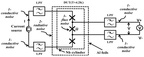
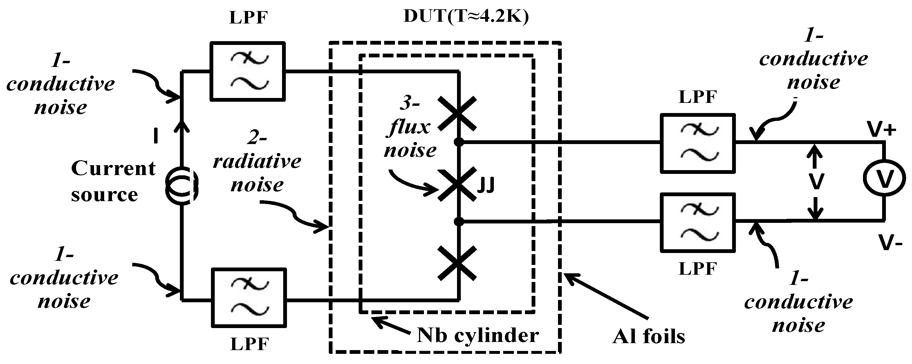
The test circuit diagram is shown in Figure 1. The JJ was submerged 10 cm below the liquid helium surface to ensure it remained in a superconducting state during I–V curve measurements. Four π-type low-pass filter (LPF) units were integrated into the circuit to suppress environmental electromagnetic (EM) noise. In typical test environments, spatial EM noise at various frequencies, including power frequency (50 Hz) and RF signals (30 kHz–30 GHz), couples into the circuit as conductive noise, thereby affecting JJ current measurements. Consequently, filtering circuits are necessary to mitigate these interference effects.
Figure 1.
Schematic of the JJ device test circuit.
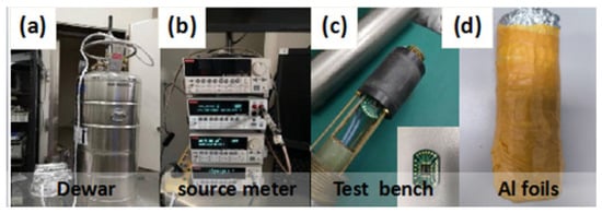
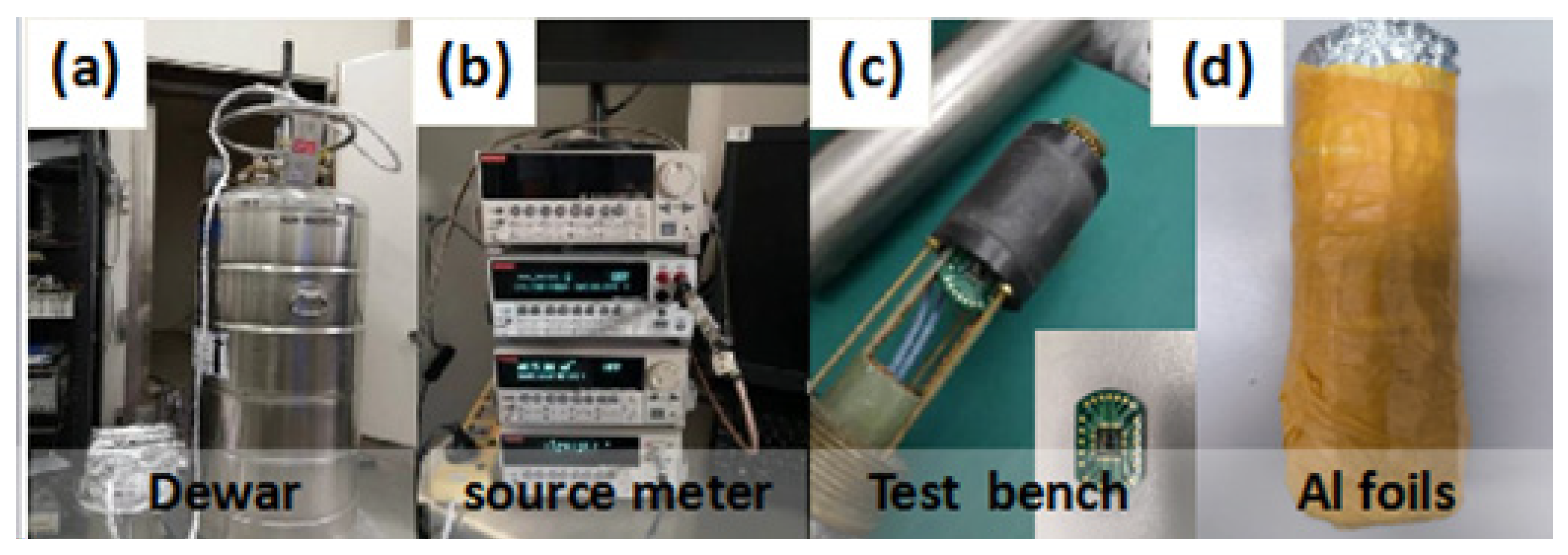
The Ic measurement setup is shown in Figure 2. A Keithley 6221 current source and a Keithley 2182A voltmeter(tektronix, Inc.US, Beaverton, OR, USA) were used to measure the I-V curve, from which the Ic value was automatically derived. The tested PCM cell was connected to the PCB via wire bonding. Ten layers of Al foil were wrapped around the Nb cylinder to shield against magnetic noise. Once the sample temperature cooled to ~4.3 K, the supply current amplitude was adjusted to twice the estimated maximum Ic, and the I–V curve was scanned and recorded by a computer. The maximum Ic is typically known from preceding current–voltage characteristic measurements. The entire experiment was controlled by a PC, with a current scanning step size of 4 µA. Further details on the testing procedure are available in our previous paper [11]. During testing, the sample was maintained below 10 cm of the liquid helium level. The de-fluxing process described herein involves: (1) raising the test rod to increase the sample temperature; (2) rotating the test rod by 90°, which may enhance the Ic value by mitigating directional magnetic field differences; and (3) maintaining the sample above 15 K for 5 min. Experimental results indicate that heating the sample to 15 K (compared to 10, 11, or 12 K for 10 s each) yields the highest Ic value. Finally, (4) the test rod is lowered to its original position for testing.
Figure 2.
Ic measurement setup: (a) test bar in Dewar; (b) current source and voltmeter; (c) test bench; (d) Al foils.
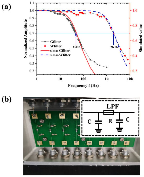
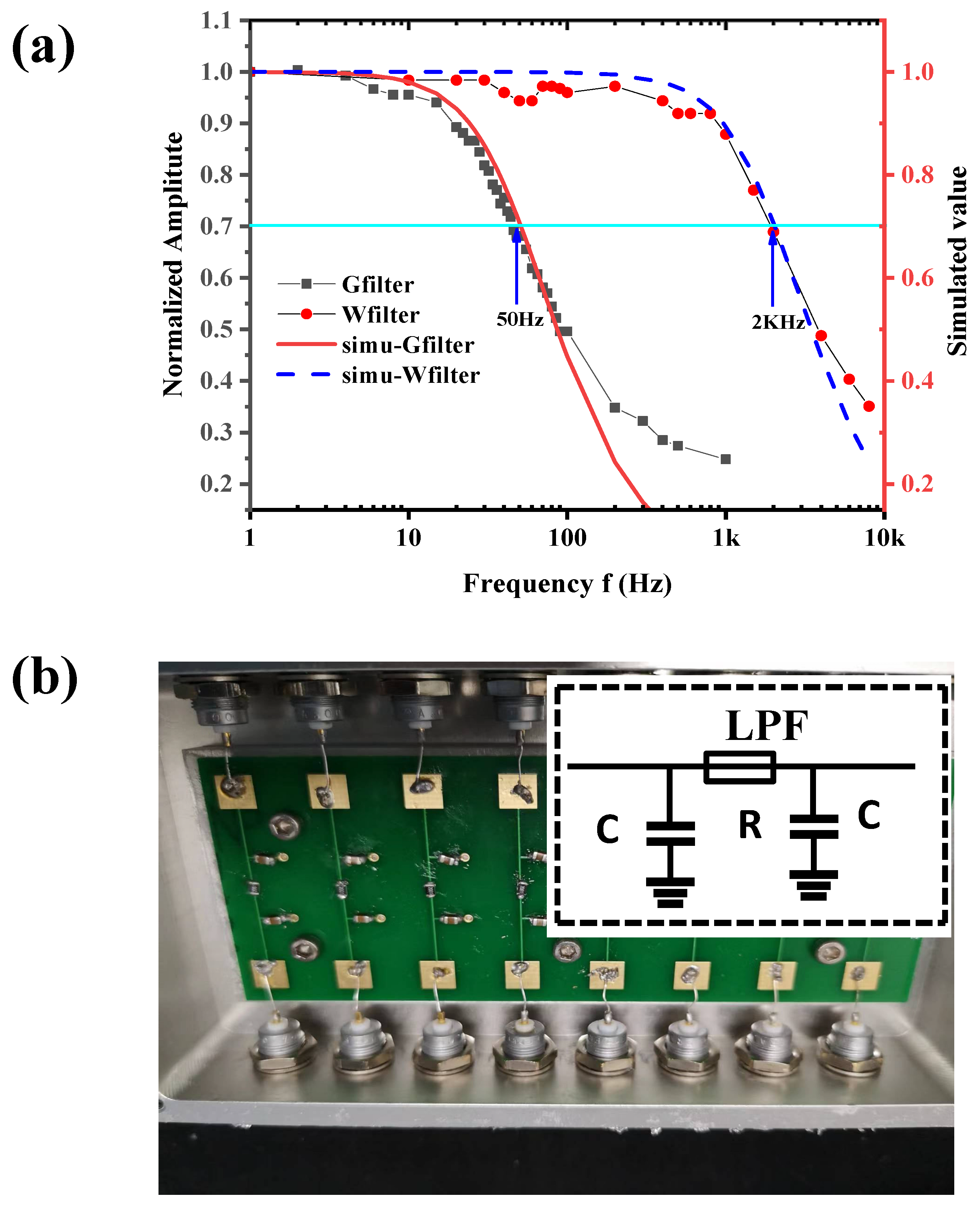
Figure 3a presents the relationship between the measured and simulated normalized output amplitudes of the filter versus frequency, while Figure 3b shows a photograph of the filter PCB. The equivalent circuit diagram of the low-pass filter is illustrated in Figure 3b. The simulated curve represents the transfer function of a first-order Butterworth filter. The cut-off frequency is determined in Figure 3a at the point where the function value is 0.707. A comparison of the experimental and simulation data for Gfilter (fc = 50 Hz) reveals good agreement below 90 Hz. However, above 90 Hz, the experimental data gradually exceeds the simulation values. Similarly, in the Wfilter (fc = 2 kHz) test, the experimental data exceeds the simulation data above 4 kHz. This discrepancy may be attributed to frequency-dependent noise interference above the cut-off frequency. To ensure effective filtering, a filter with an fc (R = 5.1 kOhm, C = 10 F) of 5 Hz was employed in this study.
Figure 3.
(a) Relationship between the measured (hexagons: 2 kHz; squares: 50 Hz) and simulated (solid line: 50 Hz; dotted line: 2 kHz) normalized output amplitude of the filter and frequency. The cut frequency is determined by the blue line. (b) Photograph of the filter PCB used for testing. Inset: Equivalent circuit diagram of the low-pass filter.
2.2. Definition of Physical Parameters Related to the Measurement of Ic
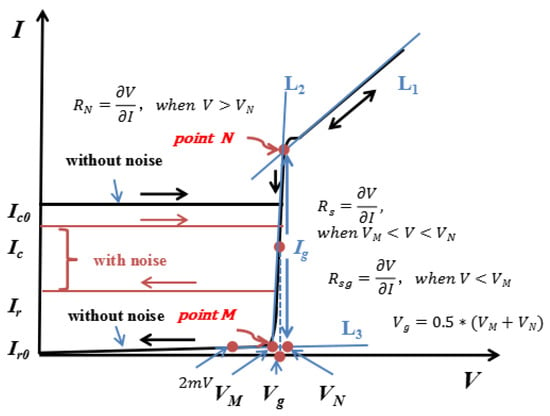
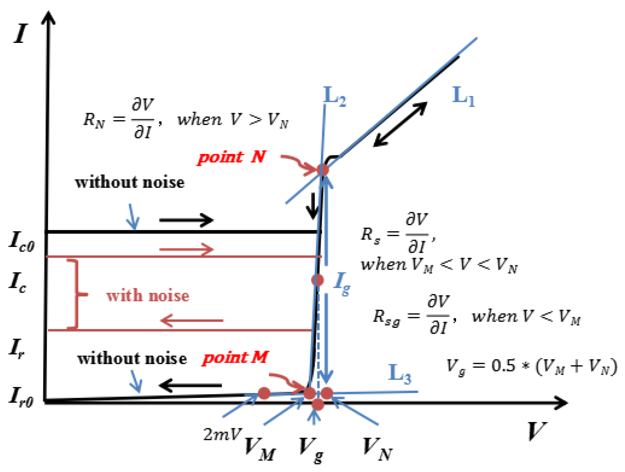
The schematic I–V curve is shown in Figure 4. The reciprocals of the slopes of L1, L2, and L3 correspond to the normal state resistance RN, semi-superconducting state resistance Rs, and sub-gap resistance Rsg, respectively. Ig is defined as the vertical coordinate of the intersection (point N) of L1 and L2. IM (=VM/Rs) is defined as the vertical coordinate of the intersection (point M) of L2 and L3. The gap voltage Vg of the JJ is defined as 2Δ/e, where e is the electron charge and Δ is the superconducting energy gap [23]. L2 shares the same slope as the –V curve in the region RsIM V RNIg. RN is the differential resistance dV/dI when V > IgRN. In this study, Rsg is the differential resistance dV/dI when V 2 mV. Vg is calculated using the formula Vg = 0.5 * (VN + VS) on line L2, where I is approximately 0.5 Ig.
Figure 4.
Schematic of the I–V curve.
In an ideal environment, the measured Ic approaches the ideal critical current Ic0, and the zero-voltage hysteresis current Ir approaches zero at 0 K. As I increases from 0 to Ic0, the voltage remains zero; when I ≥ Ic0, V increases rapidly to Vg. When I > Ig (quasi-particle current), the JJ enters the normal state with resistance RN. In practical tests, magnetic and electromagnetic noise may introduce flux into the JJ sample, thereby decreasing Ic and increasing Ir.
3. Discussion
3.1. Effect of the Low-Pass Filter with Cut-Off Frequency fc on Ic
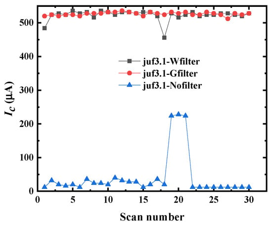
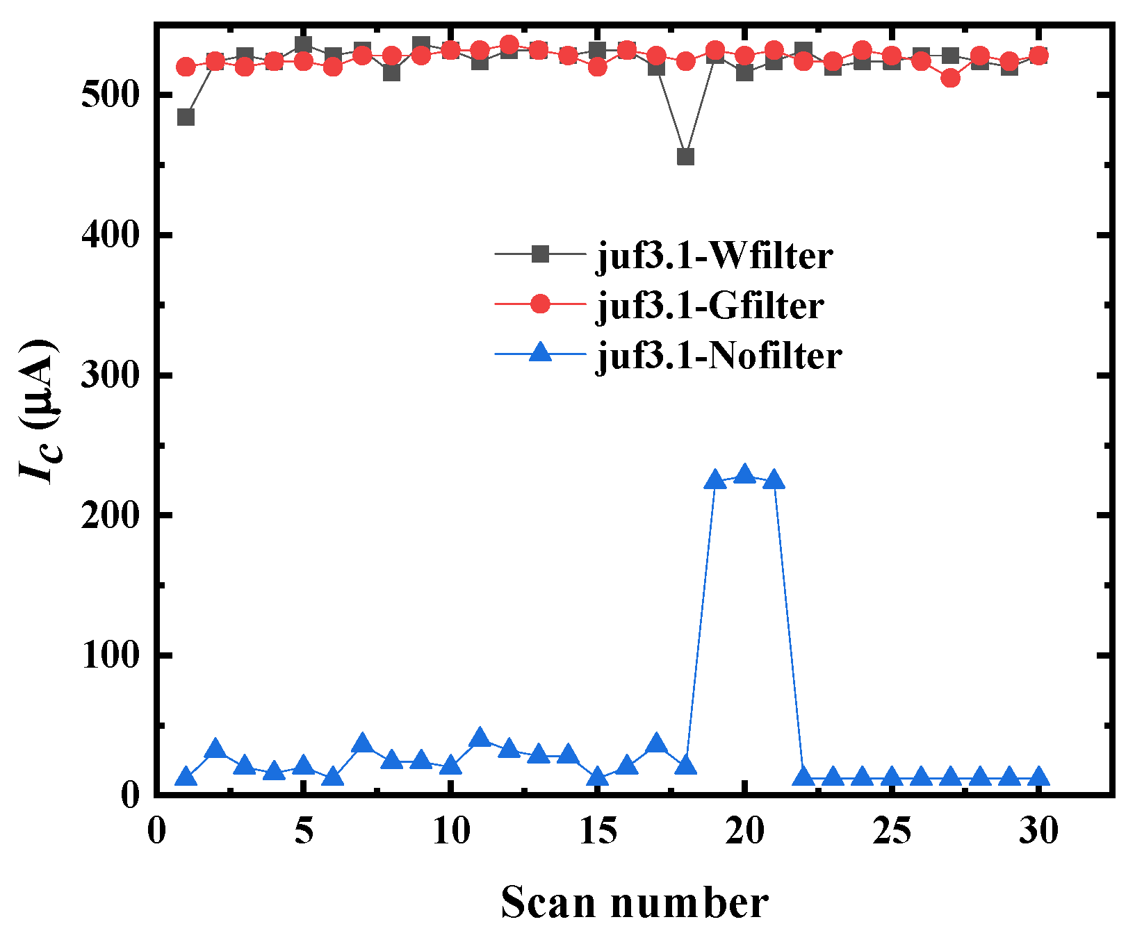
The Ic measurements for sample s0506-juf3.1, repeated 30 times for each filtering configuration outside the magnetic shield room, are shown in Figure 5. The average Ic without a filter (upward triangle) is significantly lower than that with filters, indicating that filtering is necessary to suppress conductive noise along the cables and ensure higher Ic values. The bulge in the Ic curve for the unfiltered case may be caused by the sudden disappearance of surrounding noise, which induces an increase in Ic. The Ic values without a filter appear almost constant after 22 measurements compared to those before the 21st measurement, which may be attributed to flux trapping in the unshielded environment.
Figure 5.
Ic data of sample s0506-juf3.1 from repeatability study. Gfilter: fc = 50 Hz; Wfilter: fc = 2 kHz.
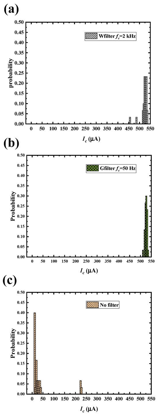
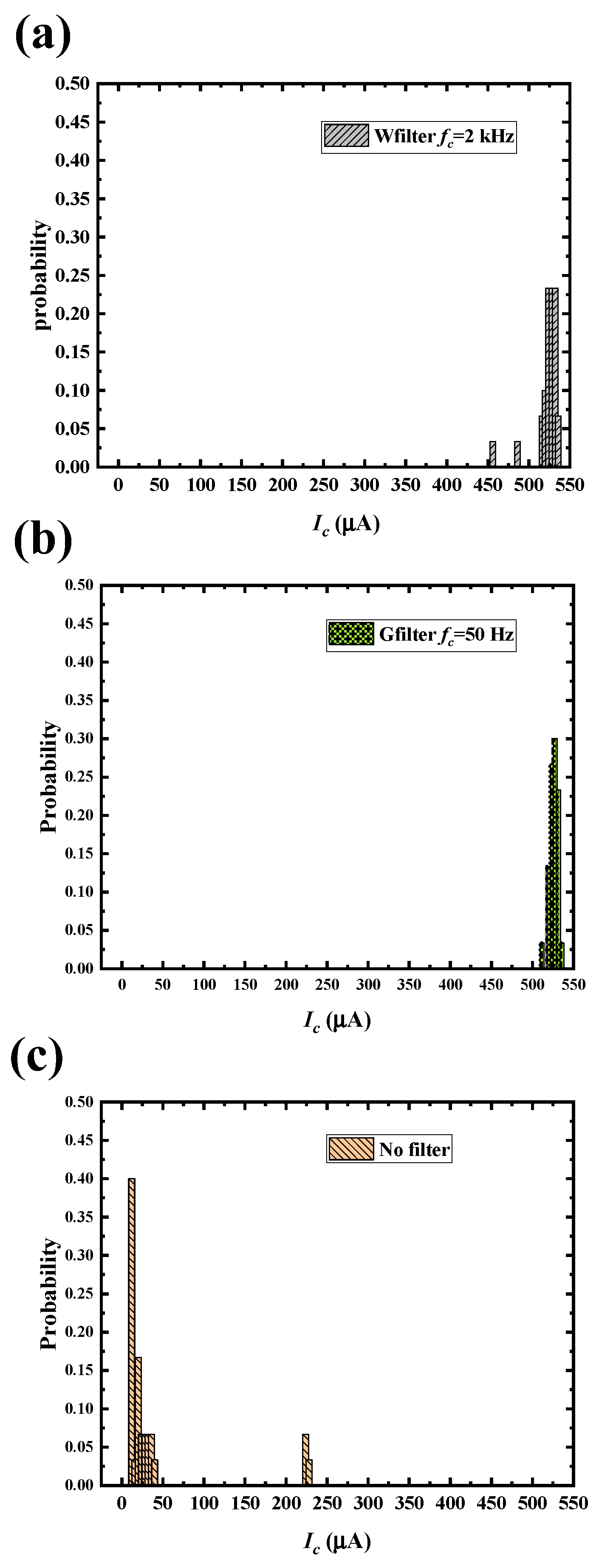
The histograms of Ic for sample s0506-juf3.1 using different filters with different cut-off frequencies are shown in Figure 6. Comparing the two curves with filter cut-off frequencies fc of 50 Hz (Gfilter, Figure 6b) and 2 kHz (Wfilter, Figure 6a) reveals that the average Ic is nearly identical (~520 μA). However, the Ic obtained with the lower cut-off frequency (fc = 50 Hz) exhibits better Ic uncertainty than that with the higher fc (2 kHz). This indicates that a filter with a lower cut-off frequency is preferable for achieving both good uncertainty and high average Ic. Electromagnetic noise, such as power frequency interference, can be filtered out by a filter with a cut-off frequency lower than 50 Hz, thereby improving the measured Ic value and reducing uncertainty.
Figure 6.
Histogram of Ic data for sample s0506-juf3.1 from the repeatability study. The filter types and cut-off frequencies are as follows: (a) Wfilter: fc = 2 kHz; (b) Gfilter: fc = 50 Hz; (c) No filter.
3.2. Effect of the Nb Cylinder and Multi-Layer Al Foils on the Measured Ic Value
Magnetic fields, flux vortices, and electromagnetic interference can penetrate superconducting films and devices through various mechanisms, leading to uncertainty in Ic measurements and ultimately affecting circuit operation. Therefore, shielding is necessary during measurements to mitigate these effects.
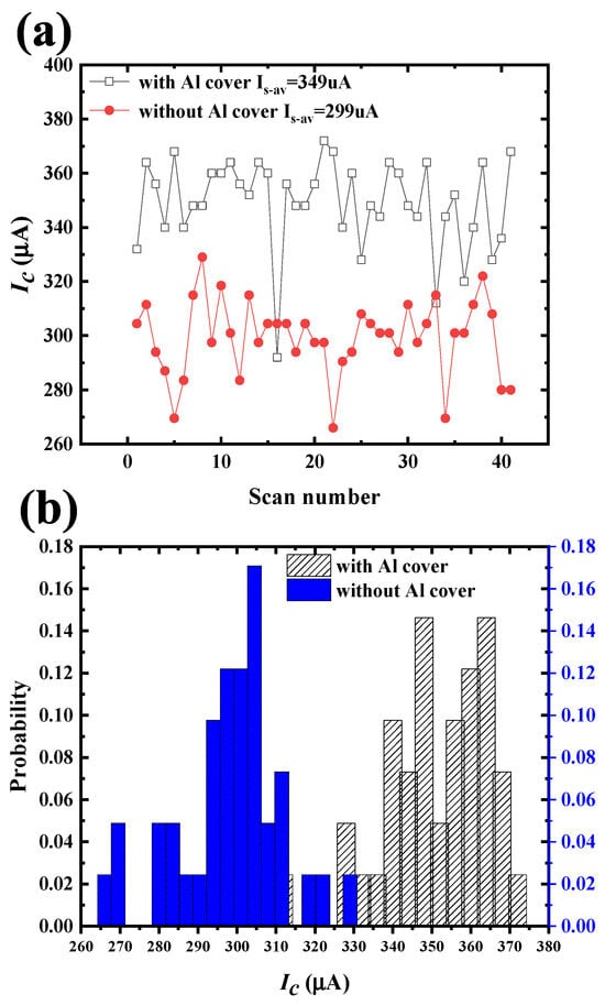
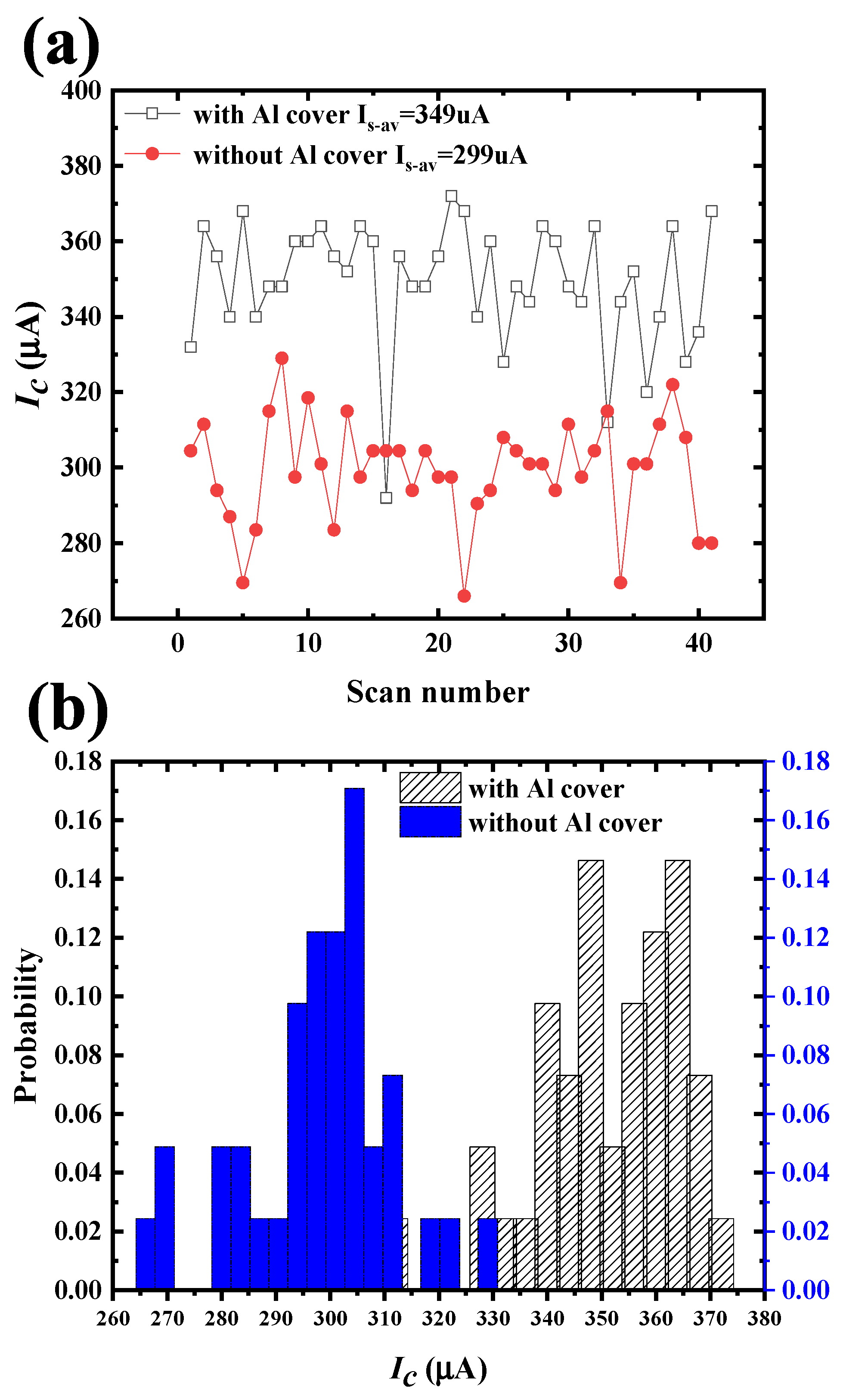
The Ic measurements for sample s0506-juf3.1, repeated 41 times with and without an Al cover, are shown in Figure 7a. The probability distributions of Ic with and without Al foils are presented in Figure 7b. The shielding structure consists of a Nb cylinder surrounded by 10 layers of Al foil. The average Ic and uncertainty with the cover are 349 μA and ±11%, respectively, whereas those without the cover are 299 μA and ±11%, respectively.
Figure 7.
(a) Ic data for sample s0506-juf3.1 from the repeatability study, measured with (blank squares) or without (full circles) Al foil; (b) Histogram of the same data with (black diagonal bars) and without (blue blank bars) Al foil.
3.3. Influence of Multiple De-Fluxing on Ic with and Without Spatial EM and Magnetic Noise
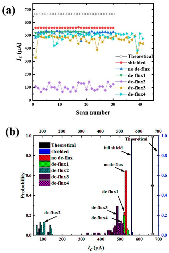
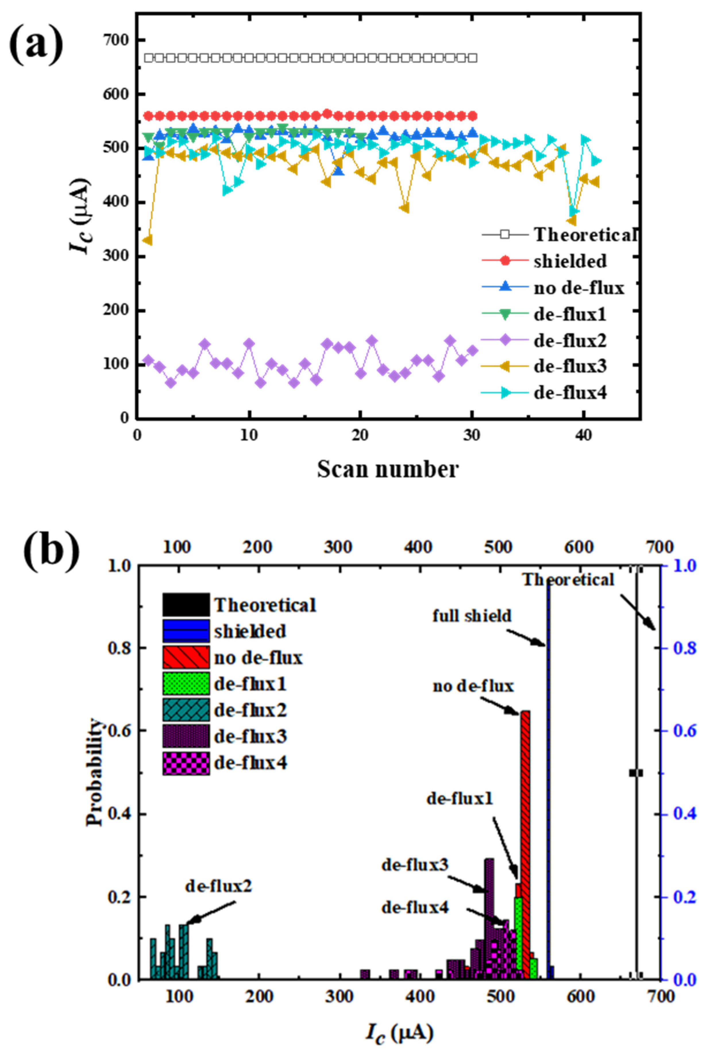
The Ic repeatability for different de-fluxing durations is presented in Figure 8a, while the histogram of the same data is shown in Figure 8b. It is evident that different de-fluxing times correspond to distinct average Ic values. Table 1 reports the uncertainty and average Ic for conditions including no de-fluxing, the first through fourth de-fluxing cycles outside the magnetic shield room, and measurements within the magnetic shield room (full shield). The average Ic after the second de-fluxing cycle is the lowest (102 μA), corresponding to the largest uncertainty. One reason for the deviation in Ic from the average Ic value outside the magnetic shield room is environmental electromagnetic (EM) noise, which may introduce flux into the sample and reduce Ic. In contrast to measurements outside the shielded room, the highest average Ic (560.13 μA) and lowest uncertainty (0.13%) were obtained within the magnetic shield room. The theoretical Ic (=Ig π/4) is calculated to be 668.82 μA.
Figure 8.
(a) Ic data of sample s0506-juf3.1 from the repeatability study, following several de-fluxing cycles; (b) histogram of the same data. Insets associate the curves with each de-fluxing cycle: theoretical data, data in full shield with no de-fluxing, and data after the first, second, third, and fourth de-fluxing cycles.
Table 1.
The uncertainty and average value of Ic with no de-fluxing, after the 1st, 2nd, 3rd, and 4th de-fluxing cycles outside the magnetic shielding room, inside the shielding room, and with theoretical Ic.
3.4. Flux Noise Impact and Its Removal or Reduction
The Ic distributions for no de-fluxing, de-flux 1, de-flux 2, de-flux 3, and de-flux 4 are shown in Figure 8b. The peak position of the Ic distribution represents the most frequently measured Ic value. Different de-fluxing cycles exhibit different Ic peak values and distributions; notably, the first de-fluxing cycle shows the maximum Ic in Figure 8a, indicating that the Ic value is not positively correlated with the number of de-fluxing cycles. Using this method, the measured Ic value under EM and magnetic noise conditions reaches 526.05 μA, which is 93.9% of the value (560.13 μA) tested in the magnetic shielding room.
As shown in Table 1, the uncertainty U of the sample varies with the number of de-fluxing cycles, and the uncertainty in the fully shielded environment is lower than that of all other tested data under unshielded conditions. The data tested under the unshielded environment also vary significantly with de-fluxing times, but the uncertainty does not show a clear positive or negative correlation with the number of de-fluxing cycles. This may be explained by the fact that spatial magnetic fields and EM noise randomly affect the flux trapping mechanism in the tested sample under unshielded conditions, thereby causing the Ic uncertainty to fluctuate. Therefore, if test conditions permit, it is necessary to perform de-fluxing in a magnetically shielded environment to reduce uncertainty.
3.5. Discussion on Circuit Scattering Noise and Thermal Fluctuations
Circuit scattering noise satisfies the central limit theorem, resulting in a Gaussian distribution of jump statistics; conversely, thermal fluctuations and thermal escape yield jump statistics that follow a Lorentzian distribution. A significant number of additional counting points appear in the tails of the histogram for thermal noise, serving as an experimental criterion to distinguish between these two noise types.
Figure 6 presents the current measurement histograms under three different cut-off frequency conditions. The histogram for the circuit with a 50 Hz cut-off frequency closely approximates a Gaussian distribution, whereas the unfiltered measurement results exhibit a Lorentzian distribution. The histogram for the 2 kHz cut-off frequency lies between these two distributions. This indicates that filters with lower cut-off frequencies more effectively suppress circuit noise, thereby yielding higher average current measurements.
3.6. Impact of Magnetic Noise and Its Mitigation
This study demonstrates that magnetic shielding reduces the influence of magnetic noise on the measurement of the junction critical current Ic by wrapping 10 layers of Al foil around the Nb cylinder enclosing the sample. General principles of magnetic and electromagnetic shielding, including the design and calculation of shielding effectiveness, are detailed in standard textbooks [24,25,26]. Iwashita et al. proposed a passive magnetic shielding method based on a niobium/aluminum structure. Theoretical analysis proves that this structure, combining high-permeability and superconducting materials, not only overcomes the shielding limit imposed by the critical field of niobium (approximately 170 mT) but also optimizes the temperature gradient of the radial thermal conductive layer, thereby enhancing the magnetic flux exclusion effect in the sample [27]. Although no experimental report was provided in the cited work, our test data for Nb/Al-AlOx/Nb samples reveal that the average Ic of the sample in the Nb cylinder wrapped with Al foil is 16.7% higher than that of the unwrapped sample (Figure 7). Experiments indicate that wrapping aluminum foil around the Nb cylinder reduces magnetic leakage and increases the probability of magnetic flux exclusion from the superconducting layer, consistent with Iwashita’s theoretical predictions. Furthermore, the current measurement distribution with Al coating tends to follow a Gaussian distribution, whereas the distribution without Al coating tends to follow a Lorentzian distribution. This suggests that the Al coating mitigates the influence of thermal fluctuations on the measurements, resulting in a relatively higher average current.
3.7. An Empirical Formula for Predicting Ic Values in Shielded Environments from Unshielded Environment Data
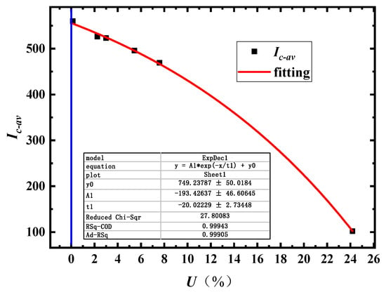
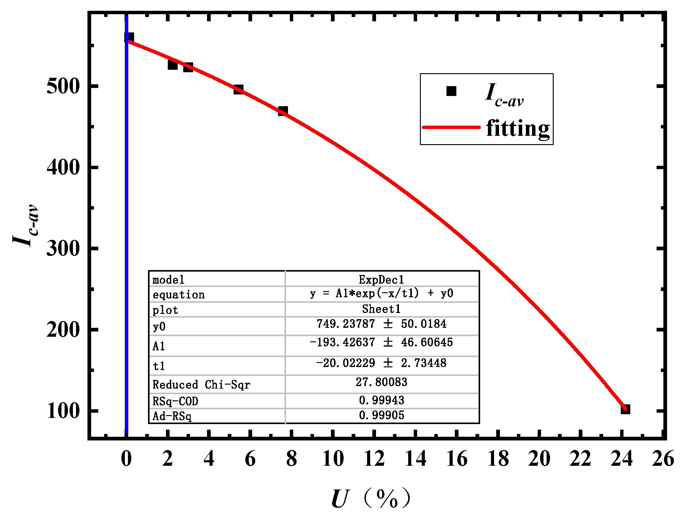
Figure 9 illustrates the relationship between the average JJ current Ic-av and the uncertainty U of the Ic data for sample s0506-juf3.1 obtained from the repeatability study. Based on the test procedure, a formula is proposed for predicting the measured Ic value in a magnetically shielded environment.
Figure 9.
Relationship between the average JJ current Ic-av and the uncertainty U of the Ic data for sample s0506-juf3.1 from the repeatability study. The red line represents the fitting curve; the red squares denote experimental data; and the blue vertical line indicates the condition where U equals 0.
The experimental procedure was as follows: (1) The sample was placed at the bottom of the testing rack; (2) the test rod was inserted into the liquid helium Dewar, maintaining the sample 10 cm below the liquid helium level during testing; (3) all devices were connected; (4) the system waited until the sample temperature dropped below 4.3 K; (5) Icij (i = 1:n; j = 1:m) was measured. Specifically, Icij was measured m times; if j < m, j was incremented by 1 and Ic was measured again; if j = m, the average value Ici-av and uncertainty Ui were obtained, and the sample was heated to de-flux. (6) n measurements of Ici-av were performed; if i < n, i was incremented by 1; if i = n, the process ended, outputting Ici-av and Ui. (7) The relationship between Ici-av and Ui was established using formula (1).
Fitting the data in Figure 9 yielded y0 = 749 μA, A1 = −193 μA, and t1 = 20. Based on the relationship between Ici-av and Ui, the average Ici was extrapolated to the point where U = 0, resulting in Ic = 556 μA. This value represents the empirical Ic under unshielded conditions. The experimentally measured Ic under shielded conditions was 560 μA. A deviation of less than 1% verifies the effectiveness of the empirical formula in predicting Ic values for sample s0506-juf3.1 in shielded environments using data from unshielded environments.
The s0506-juf2.8 sample was also measured, exhibiting a similar Ic-av versus U relationship despite having only three data points. Specifically, a larger Ic-av corresponded to smaller uncertainty, allowing the true value of Ic-av at U = 0 to be obtained through fitting.
This empirical formula is applicable to sample s0506-juf3.1. Although measurements were attempted on other samples, the data were insufficient for verification. Therefore, further validation using data from additional systems will be conducted in future work.
4. Conclusions
The influence of magnetic and electromagnetic noise on the accurate measurement of the junction critical current Ic was investigated using unshunted Nb/Al-AlOx/Nb JJ samples. Magnetic flux accumulation within the junction is the primary cause of the decrease in JJ Ic, whereas electromagnetic (EM) noise, as an external factor, mainly contributes to increased uncertainty and reduced Ic values. The specific findings are summarized as follows:
Experimental results demonstrate that magnetic flux pinning in the superconductor–insulator–superconductor (SIS) junction is a significant factor contributing to the reduction in the measured JJ current. Multiple de-fluxing procedures, involving changes in the rotation direction of the test rod before each cycle, facilitate the acquisition of higher Ic measured values. By performing repeated de-fluxing (more than five times) and selecting the optimal Ic value, the measured current reached 526.05 μA across 41 cycles, representing 93.9% of the value (560.13 μA) obtained in a shielded room. Furthermore, rotating the test rod by 90 degrees during the thermal cycle yielded a high average test current. Similar phenomena have been reported in reference [15].
The use of a Nb cylinder wrapped with multi-layer aluminum foil effectively reduces magnetic interference. This configuration increased the JJ Ic value by 16.7%.
An empirical formula was established to predict Ic values in shielded environments based on data from unshielded conditions. The deviation between the empirical Ic predictions and the experimentally measured values was less than 1%, thereby verifying the effectiveness of the proposed formula.
This study presents a relatively accurate and low-cost method for testing JJ Ic under unshielded conditions. This approach provides guidance for precise Ic measurements in conventional laboratories without expensive magnetic shielding equipment, offering significant practical value for accelerating the design and manufacturing of RSFQ devices and large-scale superconducting computer-integrated circuit chips.
5. Patents
The low-temperature superconducting Josephson junction current testing method without magnetic shielding environment and parallel resistance is attributed to Zhou Jian, Wang Juan, Wang Yongliang, and Peng Wei. Invention patent: application number: 202311206205.0; application date: 19 September 2023 Accepted. Authorization number: ZL202311206205.0; authorization date: 4 August 2026.
Author Contributions
Conceptualization, J.Z.; investigation, J.Z.; resources, Y.Y. and J.W.; writing—original draft preparation, J.Z.; writing—review and editing, Y.W.; supervision, W.P. and M.W. All authors have read and agreed to the published version of the manuscript.
Funding
This research was supported by the Strategic Priority Research Program of Chinese Academy of Sciences under Grant XDA18000000.
Data Availability Statement
All experimental data presented in this study are included in the article. Additional inquiries can be directed to the corresponding author.
Conflicts of Interest
The authors declare no conflicts of interest.
Abbreviations
The following abbreviations are used in this manuscript:
| JJ | Josephson junction |
| RSFQ | Superconducting rapid single flux quantum |
| PCMs | Process control monitors |
| PECVD | Plasma-enhanced chemical vapor deposition |
References
- Chen, W.; Rylyakov, A.V.; Patel, V.; Lukens, J.E.; Likharev, K.K. Superconductor digital frequency divider operating up to 750 GHz. Appl. Phys. Lett. 1998, 73, 2817–2819. [Google Scholar] [CrossRef] [Scilit]
- Ren, J.; Semenov, V.K. Progress with physically and logically reversible superconducting digital circuits. IEEE Trans. Appl. Supercond. 2011, 21, 780–786. [Google Scholar] [CrossRef] [Scilit]
- Tolpygo, S.K. Superconductor digital electronics: Scalability and energy efficiency issues (Review Article). Low Tem. Phys. 2016, 42, 361–379. [Google Scholar] [CrossRef] [Scilit]
- Tolpygo, S.K.; Bolkhovsky, V.; Weir, T.J.; Johnson, L.M.; Gouker, M.A.; Oliver, W.D. Fabrication process and properties of fully-planarized deep-submicron Nb/Al-AlOx/Nb Josephson junctions for VLSI circuits. IEEE Trans. Appl. Supercond. 2015, 25, 1101312. [Google Scholar] [CrossRef] [Scilit]
- Tolpygo, S.K.; Bolkhovsky, V.; Weir, T.; Wynn, A.; Oates, D.; Johnson, L.; Gouker, M.A. Advanced fabrication processes for superconducting very large scale integrated circuits. IEEE Trans. Appl. Supercond. 2016, 26, 1100110. [Google Scholar] [CrossRef] [Scilit]
- Li, F.; Peng, W. Research status and prospects of cryogenic storage for superconductor digital computing. J. Funct. Mater. Devices 2026. [Google Scholar] [CrossRef] [Scilit]
- Yang, S.C.; Chen, M.F.; Ren, J. Time scaling methodology for superconducting dual-active-layer integrated circuits. J. Funct. Mater. Devices 2026, 32, 032205. [Google Scholar] [CrossRef] [Scilit]
- Manheimer, M.A. Cryogenic computing complexity program: Phase I introduction. IEEE Trans. Appl. Supercond. 2015, 25, 1301704. [Google Scholar] [CrossRef] [Scilit]
- Yang, S.C.; Ren, J.; Gao, X.P.; Gao, Y.T.; Lin, Y.X.; Wang, M.E.; Zhao, W.B. Design automation systems for rapid single flux quantum logic. IEEE Trans. Appl. Supercond. 2026, 36, 1301105. [Google Scholar] [CrossRef] [Scilit]
- Wang, S.M.; Gao, X.; Ren, J. RCLSJ model correction and verification by a proposed test method for DFF’s high-frequency performance. Supercond. Sci. Technol. 2025, 38, 055011. [Google Scholar] [CrossRef] [Scilit]
- Gao, X.P.; Feng, Y.X.; Niu, M.H.; Gao, X.; Liu, H.L.; Weng, B.C.; Yang, S.C.; Zhang, X.; Ying, L.L.; Zhao, W.B.; et al. A 4-Nb-layer cell library suitable for LSI superconductor digital circuits. IEEE Trans. Appl. Supercond. 2025, 35, 0600405. [Google Scholar] [CrossRef] [Scilit]
- Gao, X.; Liu, H.L.; Gao, X.P.; Zhang, X.; Ren, J. Timing evaluation of passive transmission line by RSFQ ring oscillator. IEEE Trans. Appl. Supercond. 2024, 34, 1300605. [Google Scholar] [CrossRef] [Scilit]
- Tolpygo, S.K.; Bolkhovsky, V.; Zarr, S.; Weir, T.J.; Wynn, A.; Day, A.L.; Johnson, L.M.; Gouker, M.A. Properties of unshunted and resistively shunted Nb/AlOx-Al/Nb Josephson junctions with critical current densities from 0.1 to 1 mA/µm2. IEEE Trans. Appl. Supercond. 2017, 27, 2667403. [Google Scholar] [CrossRef] [Scilit]
- West, J.T.; Kurlej, A.; Wynn, A.; Rogers, C.; Gouker, M.A.; Tolpygo, S.K. Wafer-scale characterization of a superconductor integrated circuit fabrication process using a cryogenic wafer prober. IEEE Trans. Appl. Supercond. 2022, 32, 3172660. [Google Scholar] [CrossRef] [Scilit]
- Zhou, J.; Wang, J.; Yao, Y.W.; Wang, Y.L.; Wang, M.; Peng, W. A measurement method of critical current of unshunted Josephson junctions. IEEE Trans. Appl. Supercond. 2023, 33, 1–6. [Google Scholar] [CrossRef] [Scilit]
- Ambegaokar, V.; Baratoff, A. Tunneling between superconductors. Phys. Rev. Lett. 1963, 10, 486–489. [Google Scholar] [CrossRef] [Scilit]
- Ishikawa, Y.; Fukuyama, H. Effects of magnetic field on Josephson current in SNS system. J. Phys. Soc. Jpn. 1999, 68, 954–963. [Google Scholar] [CrossRef] [Scilit]
- Ohkubo, M.; Uehara, G.; Beyer, J.; Mimura, M.; Tanaka, H.; Ehara, K.; Tanaka, S.; Noguchi, T.; Mitchell, E.E.; Foley, C.P.; et al. Standard measurement method for normal state resistance and critical current of resistively shunted Josephson junction. Supercond. Sci. Technol. 2022, 35, 045002. [Google Scholar] [CrossRef] [Scilit]
- Zhang, X.; Ying, L.; Niu, M.; Zhang, H.; Liu, H.; Wu, Y.; Xu, W.; Chen, L.; Shao, Y.; Liang, T.; et al. Process control monitoring for fabrication technology of superconducting integrated circuits. IEEE Trans. Appl. Supercond. 2021, 31, 1101206. [Google Scholar] [CrossRef] [Scilit]
- Ying, L.L.; Zhang, X.; Niu, M.; Ren, J.; Peng, W.; Maezawa, M.; Wang, Z. Development of multi-layer fabrication process for SFQ large scale integrated digital circuits. IEEE Trans. Appl. Supercond. 2021, 31, 3065277. [Google Scholar] [CrossRef] [Scilit]
- Satoh, T.; Hinode, K.; Akaike, H.; Nagasawa, S.; Kitagawa, Y.; Hidaka, M. Fabrication process of planarized multi-layer Nb integrated circuit. IEEE Trans. Appl. Supercond. 2005, 15, 78–81. [Google Scholar] [CrossRef]
- Wu, Y.; Ying, L.; Li, G.; Zhang, X.; Peng, W.; Ren, J.; Wang, Z. Film stress influence on Nb/Al-AlOx/Nb Josephson junctions. IEEE Trans. Appl. Supercond. 2019, 29, 1102105. [Google Scholar] [CrossRef] [Scilit]
- Alam, S.; Jahangir, M.A.; Aziz, A. A compact model for superconductor-insulator-superconductor (SIS) Josephson junctions. IEEE Electron Device Lett. 2020, 41, 1249–1252. [Google Scholar] [CrossRef] [Scilit]
- Rikitake, T. Magnetic and Electromagnetic Shielding; Springer Science & Business Media, Kluwer: Berlin/Heidelberg, Germany, 1987. [Google Scholar]
- Celozzi, S.; Araneo, R.; Lovat, G. Electromagnetic Shielding; IEEE Press and Wiley Interscience (Wiley): Hoboken, NJ, USA, 2008. [Google Scholar]
- Braginski, A.I. Superconductor electronics: Status and outlook. J. Supercond. Nov. Magn. 2019, 32, 23–44. [Google Scholar] [CrossRef] [Scilit]
- Iwashita, Y.; Kuriyama, Y.; Tongu, H.; Fuwa, Y. Magnetic field shielding with superconductors. IEEE Trans. Appl. Supercond. 2022, 32, 3500404. [Google Scholar] [CrossRef] [Scilit]

Disclaimer/Publisher’s Note: The statements, opinions and data contained in all publications are solely those of the individual author(s) and contributor(s) and not of MDPI and/or the editor(s). MDPI and/or the editor(s) disclaim responsibility for any injury to people or property resulting from any ideas, methods, instructions or products referred to in the content. |
© 2026 by the authors. Licensee MDPI, Basel, Switzerland. This article is an open access article distributed under the terms and conditions of the Creative Commons Attribution (CC BY) license.