


Abstract
Polytetrafluoroethylene (PTFE) is an important dielectric and structural substrate for high-frequency, flexible, low-background, and other electronic systems because of its low dielectric loss, high electrical resistivity, low moisture absorption, chemical inertness, and thermal stability. However, its fluorine-rich surface, low surface energy, and weak boundary layer hinder metal nucleation and interfacial bonding, frequently leading to discontinuous film growth, high interfacial resistance, and premature delamination. This focused review summarizes recent progress in low-temperature plasma-assisted metallization of PTFE, with particular emphasis on the relationships among plasma activation, interface formation, electrical functionality, reliability, and manufacturability. The effects of plasma-induced physical etching, defluorination, radical generation, polar functionalization, weak-boundary-layer removal, and hydrophobic recovery are first discussed. Representative metallization routes are then reviewed, including direct physical vapor deposition, plasma-assisted electroless plating, plasma-induced grafting, metallic interlayers, ion implantation, and hybrid plasma-deposition processes. Particular attention is given to interface-strengthening mechanisms involving chemical bonding, mechanical interlocking, diffusion control, carbon-rich or graded transition regions, and interdiffusion. The key trade-offs among adhesion strength, conductor resistance, dielectric integrity, surface-modification stability, and mechanical or environmental reliability are further analyzed for electronic-substrate applications. Although metallic interlayers, ion implantation, and hybrid processes can provide more stable interfaces than plasma activation alone, challenges remain in controlling plasma-induced damage, surface aging, interfacial carbonization, and process reproducibility. Recent 2024–2026 studies further show that these interface technologies can translate into low-loss Cu/PTFE laminates, flexible circuits, integrated vacuum metallization stacks, and selectively patterned conductors. The relevance to low-power systems is therefore treated as one application context at the substrate/interconnect level rather than as evidence that PTFE metallization directly reduces circuit switching power.
1. Introduction
The continuing development of high-frequency, flexible, miniaturized, low-background, and environmentally robust electronic systems has increased the importance of substrate, dielectric, and interconnect interfaces in determining electrical performance and long-term reliability. Passive losses associated with conductor resistance, dielectric polarization, interfacial defects, leakage, and environmental degradation can influence signal integrity and energy efficiency even though active-device switching power and circuit architecture are determined elsewhere. Polytetrafluoroethylene (PTFE) is attractive for such applications because of its low dielectric constant and dielectric loss, high electrical resistivity, low moisture absorption, excellent chemical stability, and thermal resistance [1,2,3]. PTFE and PTFE-based composites have consequently been investigated as substrates or insulating components in flexible circuits, high-frequency printed wiring boards, sensing structures, low-background electronic systems, and other conductor-bearing platforms [4,5]. Low-power electronics remains one relevant application context, particularly where leakage, passive conductor loss, and reliability are important, but it is not treated here as the defining scope of PTFE metallization. Figure 1 summarizes this structure-property relationship: the fluorocarbon molecular architecture that gives PTFE its low-loss, chemically inert, and thermally stable character also underlies the low surface energy and limited chemical reactivity that make reliable metallization difficult.
Figure 1.
Molecular structure and key properties of PTFE relevant to electronic substrates. (a) Polymerization of tetrafluoroethylene and the molecular structure of PTFE; (b) Key physical, thermal, electrical, chemical, and mechanical properties of PTFE [2].
The same molecular structure that provides PTFE with its desirable dielectric and chemical properties, however, makes its surface exceptionally difficult to metallize. The carbon backbone of PTFE is surrounded by densely packed fluorine atoms, while the high bond energy of the C-F bond gives the polymer pronounced chemical inertness [3]. Pristine PTFE therefore exhibits a low surface energy, strong hydrophobicity, limited interaction with deposited atoms, and a scarcity of chemically active sites for metal nucleation [6,7]. In addition, machining, surface contamination, molecular rearrangement, or loosely bonded fluorocarbon fragments may produce a weak boundary layer near the PTFE surface [8]. When a metal is deposited directly onto such an inert and mechanically weak surface, metal-metal interactions may dominate over metal-substrate interactions. The deposited atoms consequently tend to aggregate into isolated islands before forming a continuous film, which may lead to interfacial voids, delayed film coalescence, stress concentration, increased electrical resistance, and poor adhesion [9]. These defects can be further amplified during bending, thermal cycling, humidity exposure, or operation under harsh environmental conditions, ultimately resulting in cracking, resistance drift, and delamination.
As summarized in Figure 2, adhesion at metal/PTFE interfaces can involve mechanical interlocking, electrostatic attraction, and, importantly, chemical bonding between deposited metal or interlayer species and plasma-generated functional groups. Effective PTFE metallization therefore requires modification of the near-surface region while preserving the intrinsic dielectric and insulating properties of the bulk polymer. Conventional wet-chemical treatments can promote defluorination and increase surface reactivity, but they often rely on highly reactive chemical agents and may involve nonuniform etching, residual contamination, additional cleaning procedures, and environmental concerns [6,9]. Low-temperature plasma treatment provides a dry and comparatively controllable alternative. In a non-equilibrium plasma, energetic electrons coexist with ions and neutral species at relatively low gas temperatures, allowing chemically and physically active particles to modify the outermost surface without imposing excessive thermal loading on the polymer. Plasma-generated ions, electrons, radicals, and excited neutral species can break C-F and C-C bonds, promote surface defluorination, generate carbon-centered radicals and unsaturated structures, remove weakly bonded fragments, and modify the surface morphology at micro- or nanoscale dimensions [10,11].
Figure 2.
Representative adhesion mechanisms at metal-polymer interfaces. (a) Mechanical interlocking produced by surface roughening or interpenetration; (b) electrostatic interaction across the interface; (c) chemical bonding between deposited metal/interlayer species and plasma-generated polar sites on PTFE, illustrated schematically by M–O–C and related interfacial bonds.
In addition to physical bombardment, plasma treatment can introduce chemically active functional groups through reactions involving oxygen-, nitrogen-, or water-containing species. Depending on the working gas and treatment conditions, C-O, C=O, O-C=O, C-N, and N-H groups may be generated on the activated PTFE surface, thereby increasing its polarity and providing potential bonding or nucleation sites for deposited metals [10,11,12]. The relative contributions of physical etching and chemical functionalization depend strongly on the plasma source, discharge pressure, power density, treatment duration, gas composition, and substrate temperature. Comparative investigations of radio-frequency and dielectric-barrier-discharge plasmas have shown that differences in particle energy and collision frequency can result in substantially different degrees of defluorination, roughening, and functional-group incorporation [10]. Argon plasma primarily promotes physical sputtering, weak-boundary-layer removal, and radical generation, whereas O2, N2, H2O, or their mixtures can contribute to the controlled incorporation of oxygen- or nitrogen-containing groups [11,12]. In mixed Ar/H2O plasma, for example, argon-induced bombardment exposes reactive carbon sites, while water-derived species assist surface functionalization and suppress the formation of weakly bonded fluorocarbon deposits, resulting in improved metal/PTFE adhesion [13]. Plasma activation should therefore be regarded as a coordinated process involving surface cleaning, bond scission, radical formation, chemical functionalization, and morphological reconstruction rather than merely as a roughening treatment.
A major limitation of plasma-modified polymer surfaces is their time-dependent aging behavior. After plasma exposure, surface radicals may recombine, low-molecular-weight fragments may migrate, airborne contaminants may adsorb, and polar groups may rotate or diffuse toward the subsurface as the polymer seeks to minimize its surface free energy [14]. This hydrophobic recovery can reduce surface polarity and narrow the processing window available for subsequent metal deposition. Consequently, the storage time and environmental conditions between plasma activation and metallization can strongly affect interfacial reproducibility. Plasma-induced graft polymerization has been investigated as a strategy for stabilizing the activated PTFE surface. In this process, plasma-generated radicals initiate the attachment or growth of functional polymer chains, such as poly (acrylic acid), containing carboxyl or other polar groups [15,16]. The grafted layer can suppress surface-chain rearrangement, maintain reactive sites for a longer period, and improve the durability of surface activation. Nevertheless, enhanced wettability alone does not guarantee improved electronic performance. The thickness, continuity, thermal stability, electrical insulation, and dielectric characteristics of the grafted layer must also be considered when the modified PTFE is used as an electronic substrate.
Following plasma activation, metallic layers can be formed by physical vapor deposition, electroless plating, lamination, or combinations of these processes. Direct physical deposition offers a relatively simple and clean process route, but its success depends strongly on the density, chemical nature, and stability of plasma-generated surface sites [9]. Plasma-assisted electroless plating can enhance metal nucleation by immobilizing catalytic species on functionalized polymer surfaces and can be advantageous for conformal or selectively patterned conductive layers [17]. For applications requiring greater interfacial stability, metallic interlayers such as Ni, Cr, or Ti may be introduced between PTFE and the main conductive layer. These interlayers can form chemical bonds with plasma-generated surface groups, inhibit uncontrolled diffusion of Cu into the polymer, accommodate interfacial stress, and provide a more compatible surface for subsequent conductor growth [18]. Their effectiveness, however, depends on composition, thickness, oxidation state, and compatibility with both the polymer substrate and the deposited conductor.
Ion implantation and plasma-immersion ion implantation provide an alternative approach by modifying the subsurface region rather than only the outermost surface. Implantation of metallic or nitrogen ions can induce C-F bond cleavage, defluorination, carbon-rich or unsaturated structures, C-N bonding, and the formation of metal fluorides or carbides [4,19,20]. Because the implanted region extends beneath the original surface, it may serve as a graded transition zone that promotes chemical bonding, mechanical interlocking, and stress transfer between PTFE and the deposited metal. Hybrid processes combining plasma activation with metallic transition layers, catalytic seeding, electroless deposition, or heat-assisted lamination have also demonstrated substantial improvements in metal/PTFE adhesion [5,17,21]. In optimized structures, the failure mode may change from interfacial separation to cohesive fracture within the PTFE substrate, indicating that the interface is no longer the weakest region of the metal-polymer system.
For electronic-substrate applications, metallization strategies should not be evaluated solely by contact angle or peel strength. The electrical resistance of the deposited metal, the stability of metal continuity under deformation, interfacial contact resistance, dielectric integrity, leakage behavior, and resistance to environmental aging are equally important. Aggressive plasma bombardment may improve adhesion through roughening and carbonization, but excessive surface damage may alter the insulating behavior or dielectric properties of PTFE [4,19,20]. Similarly, a metallic interlayer may enhance bonding and suppress diffusion, yet an excessively thick, oxidized, or resistive layer may increase the effective resistance of the conductive stack. Grafted organic layers may provide stable surface functionality but also introduce an additional dielectric or electrically resistive interface. The optimum metallization process therefore requires a balance among adhesion, conductivity, dielectric performance, flexibility, environmental stability, and manufacturing compatibility.
Existing reviews have provided broad discussions of PTFE properties, fluoropolymer surface modification, and polymer metallization technologies [2,9]. However, surface activation, metal deposition, interfacial strengthening, and electronic-substrate performance are often treated as separate topics. The present focused review examines low-temperature plasma-assisted metallization of PTFE from an integrated process-interface-property perspective. It first discusses plasma-induced physical etching, defluorination, chemical functionalization, weak-boundary-layer removal, surface aging, and grade-dependent response. It then compares direct deposition, plasma-induced grafting, metallic and carbon-containing interlayers, ion implantation, plasma-assisted electroless plating, and hybrid metallization routes. Particular emphasis is placed on the relationships among plasma-processing parameters, interfacial structure, metal nucleation, adhesion, electrical resistance, dielectric integrity, and mechanical or environmental reliability. Most published studies remain at the material or coupon level, and direct demonstrations linking a specific PTFE metallization process to circuit-level power consumption are scarce. Accordingly, electronic functionality is evaluated primarily in terms of substrate and interconnect performance, while low-power electronics is treated as one application context rather than the defining scope. A dedicated manufacturing-oriented discussion in Section 4.6 connects the reviewed interface technologies to practical substrate functions and fabrication routes.
2. Plasma-Induced Surface Activation
Low-temperature plasma activation is a critical upstream step in the metallization of PTFE because it determines the initial nucleation behavior of the deposited metal and the chemical and mechanical stability of the resulting interface. For electronic-substrate applications, the objective is not simply to maximize surface wettability or roughness, but to create a thin, chemically active, and mechanically stable surface region while retaining the electrical insulation and dielectric characteristics of the bulk polymer [22]. Plasma treatment offers a particularly useful route because the incident ions, electrons, radicals, and excited neutral species can simultaneously clean, etch, functionalize, and restructure the outermost PTFE surface without requiring extensive wet-chemical processing [10,23]. Nevertheless, these mechanisms are strongly coupled, and their relative contributions depend on the plasma source, gas composition, treatment time, pressure, power density, and post-treatment environment. Figure 3 organizes these coupled effects into two complementary views-the molecular-level pathways of PTFE activation and the principal low-temperature plasma routes used to create or stabilize reactive surface states—and therefore provides the mechanistic framework for the discussion in Section 2.1, Section 2.2, Section 2.3 and Section 2.4.
Figure 3.
Molecular mechanisms and low-temperature plasma routes for PTFE surface activation and functionalization. (a) Possible molecular pathways of plasma-induced bond cleavage, radical formation, unsaturated-structure generation, and subsequent functionalization of PTFE [24]; (b) Low-temperature plasma routes for PTFE surface activation and functionalization, including direct plasma treatment, plasma polymerization, plasma syn-irradiation, and plasma-induced grafting.
2.1. Activation Mechanisms and Processing Window
The initial interaction between plasma species and PTFE primarily involves energy transfer to the fluorocarbon chains. Energetic ions and neutral species can break C-F and C-C bonds, release fluorine-containing fragments, and produce carbon-centered radicals and unsaturated structures at the surface [10,11]. The loss of fluorine reduces the chemical shielding of the carbon backbone and generates sites that can subsequently react with plasma-derived species or atmospheric O2, H2O, and N2. Depending on the treatment atmosphere, the activated surface may therefore contain C-O, C=O, O-C=O, C-N, N-H, and other polar groups. These chemical changes increase surface polarity and can provide adsorption, coordination, or chemical-bonding sites for subsequently deposited metals.
Physical bombardment occurs concurrently with chemical activation. Ion-induced sputtering removes adsorbed contamination, loosely bonded fluorocarbon fragments, and the weak boundary layer that may form during PTFE molding, machining, storage, or handling [8]. The removal of this mechanically unstable region is particularly important because an apparently strong metal-surface interaction cannot produce a reliable structure if fracture occurs within a weak subsurface layer. Plasma etching may also generate micro- or nanoscale topographical features that increase the effective interfacial area and provide sites for mechanical interlocking. Thus, the improvement in metal adhesion usually results from the combined effects of surface cleaning, weak-boundary-layer removal, chemical functionalization, and morphological reconstruction rather than from a single mechanism.
The relative importance of these processes defines a plasma-processing window. At insufficient energy or short treatment time, the degree of defluorination and the density of reactive sites may remain too low to promote uniform metal nucleation. At excessive energy or prolonged treatment, however, chain scission, mass loss, roughness development, carbonization, and the formation of low-molecular-weight fragments may weaken the near-surface region. High plasma power should therefore not automatically be interpreted as favorable. A surface with a very low water contact angle may still be unsuitable for electronic metallization if it contains weak oxidation products, excessive damage, or an electrically altered carbon-rich layer.
Recent work further illustrates that activation efficiency does not require high ion bombardment. Komlev et al. used a low-power DC glow discharge with a fast-neutral source and reported a PTFE water contact angle of approximately 13° and surface energy of about 82 mN m−1 at a discharge power of only ~6 W [25]. Because fast ions were largely suppressed, the approach was designed to limit charging and sputter damage while retaining UV- and neutral-assisted defluorination. Although direct metallization was not evaluated in that study, it provides a recent PTFE-specific example of a low-damage activation window that is relevant to subsequent conductor deposition.
For this reason, plasma-treated PTFE should be evaluated using complementary indicators. Contact-angle measurements provide a convenient measure of wettability but do not identify the origin or stability of the modification. X-ray photoelectron spectroscopy is needed to determine the degree of defluorination and the formation of oxygen- or nitrogen-containing groups, whereas atomic-force or electron microscopy can reveal roughening, etching, or polishing. Aging measurements are necessary to establish whether the activated state persists long enough for subsequent metal deposition. For electronic applications, these surface measurements should ultimately be combined with tests of insulation resistance, dielectric properties, metal continuity, adhesion, and environmental reliability.
2.2. Gas-Dependent Physical Etching and Chemical Functionalization
The working gas determines both the energy-transfer pathway and the chemistry of the activated PTFE surface. Oxygen plasma is widely used because oxygen radicals can react with carbon-centered sites formed after C-F or C-C bond cleavage. Liu et al. compared radio-frequency oxygen plasma with atmospheric-pressure dielectric-barrier-discharge plasma and showed that the two sources produced substantially different surface states [10]. Under low-pressure RF conditions, energetic particle bombardment produced pronounced defluorination, surface roughening, and incorporation of oxygen-containing groups. By contrast, the greater collision frequency under atmospheric DBD conditions reduced the energy of species arriving at the surface, resulting in less extensive bond cleavage and morphological change. The DBD treatment nevertheless introduced sufficient polar groups to improve surface activation. This comparison demonstrates that plasma-source selection controls not only treatment efficiency but also the balance between chemical functionalization and physical damage.
Nitrogen-containing plasmas can provide an alternative surface chemistry. XPS studies of oxygen- and nitrogen-plasma-treated PTFE have shown that both atmospheres can induce defluorination, while nitrogen plasma additionally enables the formation of C-N- and N-H-related species [11,26]. These nitrogen-containing sites may interact with metal atoms or catalytic ions and are therefore potentially useful for subsequent physical deposition or electroless plating. In a comparative atmospheric-plasma study, short treatments using N2, O2, and Ar/H2 all reduced the water contact angle of PTFE, but the N2 treatment produced the largest decrease, from 141.9° to 109.5°, compared with 119.8° for O2 and 117.1° for Ar/H2 [27]. The optimum treatment time was approximately 2 min; longer exposure did not further improve wettability and instead increased the risk of surface damage. All three treatments produced defluorination and oxygen-containing species, probably because of residual gases and post-treatment oxidation, whereas nitrogen plasma also introduced nitrogen-containing functionalities [27].
Argon and other inert-gas plasmas primarily activate PTFE through physical energy transfer. Ar-ion bombardment can remove the weak boundary layer, cleave C-F bonds, generate surface radicals, and alter roughness without directly supplying a new functional element [12,28,29]. The final surface composition after Ar treatment therefore depends strongly on residual gases and subsequent exposure to air. Carbon-centered radicals formed under Ar plasma may recombine with one another, form unsaturated structures, or react with O2, H2O, and N2 after removal from the plasma chamber. Consequently, oxygen or nitrogen detected on an Ar-treated PTFE surface does not necessarily originate from the nominal working gas.
This behavior is evident in studies using low-pressure, atmospheric-pressure, and inductively coupled Ar plasmas. Lin et al. reported that cold atmospheric-pressure Ar plasma reduced the water contact angle of PTFE from 91.1° to 37.4° and increased the polar component of the surface free energy from 3.3 to 46.7 mJ m−2 [30]. The relative CF2 concentration decreased, whereas C-O and C=O species increased, indicating that physical activation by Ar was followed by reactions with residual or atmospheric oxygen-containing species. Similarly, ferromagnetic-enhanced inductively coupled Ar plasma reduced the water contact angle from 122° to 59° and produced C-O- and C-N-related bonding, even though neither oxygen nor nitrogen was intentionally used as the primary working gas [31]. The latter species were attributed to trace gases, leakage, water vapor, or post-plasma exposure.
Although pure Ar plasma can efficiently clean and activate PTFE, the density and identity of the resulting functional groups are difficult to control. The intentional addition of a small quantity of reactive gas is therefore an effective method for combining physical etching with controlled chemical functionalization. H2O/Ar plasma is a representative example [12,13]. Ar species provide momentum transfer and remove the weak surface region, whereas dissociation of water generates H, OH, and oxygen-containing species. These reactive species can terminate surface radicals, introduce C-O, C=O, and O-C=O groups, and inhibit the accumulation of loosely bonded CxFγ fragments.
Ohkubo et al. compared open-air Ar and Ar/H2O plasma treatments before the direct formation of Ag wiring on PTFE [13]. After 600 s of Ar/H2O treatment, the Ag/PTFE peel strength increased to 1.03 N mm−1, compared with only 0.06 N mm−1 after pure Ar treatment. The value also exceeded the cited industrial requirement of 0.70 N mm−1. The improvement was attributed to the combined removal of the weak boundary layer, suppression of unstable fluorocarbon deposits, and formation of oxygen-containing groups capable of strengthening the Ag/PTFE interface. This result illustrates that wettability alone is not the decisive indicator: two plasma treatments may generate both radicals and surface etching, yet only the treatment producing a chemically stable surface can support strong metallization.
The effects of plasma exposure are not always monotonic. Depending on the initial surface, plasma conditions, and competition between etching and functionalization, roughness may increase, decrease, or develop into a hierarchical morphology. Kang et al. showed that Ar- and O2-plasma etching could increase the water contact angle of PTFE from 113.8 ± 1.4° to 172.5 ± 1.2° when the treatment changed the morphology without introducing a sufficient concentration of polar groups [32]. The resulting micro/nanoscale structure amplified the intrinsic hydrophobicity of PTFE. Other studies have reported a plasma-induced polishing effect, in which prolonged exposure removes protrusions and reduces roughness [30,31]. These observations show that plasma etching cannot be assumed to increase either roughness or wettability under all conditions.
The practical implication is that gas composition should be selected according to the required interfacial function. Pure inert-gas plasma is useful for cleaning, radical generation, and removal of the weak boundary layer. Reactive plasma is useful for introducing chemically active groups. Mixed inert/reactive gases can combine these functions and provide greater control over the activated state. For low-power electronic substrates, the preferred condition is not necessarily the one producing the greatest etch depth, but the one generating a high density of stable bonding sites with minimal modification of the bulk electrical properties.
Table 1 summarizes the gas- and plasma-source-dependent activation behavior discussed above, providing a direct comparison of the dominant activation mechanism, changes in wettability and surface chemistry, implications for metal adhesion, and the principal limitation of each treatment route. This comparison highlights why plasma selection should be based on the required interfacial function rather than on wettability improvement alone.
Table 1.
Effects of Plasma Source and Working Gas on PTFE Surface Activation.
2.3. Surface Aging and Hydrophobic Recovery
The activated state of PTFE is generally thermodynamically unstable. Immediately after plasma treatment, the surface contains radicals, polar groups, unsaturated carbon structures, chain fragments, and nonequilibrium molecular configurations. During storage, these species undergo further reactions that gradually reduce surface polarity. Radical recombination consumes active sites, while reactions among oxygen-containing groups may form volatile or weakly bound low-molecular-weight products. Surface contamination from the surrounding atmosphere can also mask polar groups.
A particularly important mechanism is the reorientation and migration of polymer segments. Polar groups formed at the surface may rotate or migrate toward the subsurface, while fluorinated chain segments reappear at the outer interface to minimize the surface free energy [14,33]. Low-molecular-weight oxidation products and additives may also diffuse between the bulk and the surface. The combined effect is commonly observed as an increase in water contact angle with storage time. For example, the contact angle of Ar-plasma-treated PTFE increased from 59° after treatment to approximately 78° after 10 days of air storage [31]. Although the surface remained more wettable than untreated PTFE, the result demonstrates that the effective metallization window progressively narrows after activation.
Hydrophobic recovery has direct manufacturing consequences. Variations in the delay between plasma treatment and metal deposition can lead to variations in metal nucleation, film continuity, and peel strength even when the nominal plasma parameters are unchanged. The storage atmosphere, temperature, humidity, and surface contamination history should therefore be reported together with the plasma conditions. Whenever possible, cleaning, activation, interlayer deposition, and conductor deposition should be integrated into a continuous process with limited air exposure. When such integration is impractical, a more durable surface-stabilization strategy is required.
2.4. Plasma-Induced Grafting for Durable Activation
Plasma-induced grafting stabilizes the activated PTFE surface by converting short-lived radicals into covalently attached functional layers. The process usually involves plasma generation of radical sites followed by contact with a gaseous or liquid monomer. Polymerization initiated from these surface sites produces polymer chains or crosslinked networks that contain a high density of functional groups. In addition to providing sites for metal nucleation or catalytic-ion attachment, the grafted layer physically restricts the reorientation of the underlying PTFE chains and thereby suppresses hydrophobic recovery.
Acrylic acid is one of the most frequently used grafting monomers because it polymerizes readily and provides carboxyl groups. Ji et al. treated PTFE in a He/acrylic-acid atmosphere using atmospheric-pressure DBD plasma [34]. The water contact angle decreased from 109.9° to 67.8°, and a nanoscale poly (acrylic acid) layer remained after ultrasonic cleaning in acetone, indicating that the deposited material was chemically attached rather than only physically adsorbed. This direct plasma-monomer approach is relatively rapid, although the resulting layer may be thin and its uniformity depends on the spatial distribution of plasma energy and monomer fragments.
Hori et al. similarly used atmospheric-pressure Ar plasma in the presence of acrylic acid and introduced carboxyl and carbonyl groups onto PTFE [35]. In that study, however, the grafted material appeared as discontinuous islands rather than a fully continuous layer. Such spatial nonuniformity is important for metallization because a heterogeneous distribution of functional groups may produce nonuniform metal nucleation, local variations in contact resistance, and weak regions in the final coating. The result also illustrates that the same nominal monomer can produce different surface structures depending on the plasma source, treatment geometry, monomer delivery, and energy distribution.
A second route separates plasma activation from graft polymerization. PTFE is first exposed to plasma to generate radicals or peroxide precursors and is subsequently immersed in a monomer solution. Low-pressure H2O plasma followed by acrylic-acid grafting has been shown to produce durable PTFE modification [36]. Compared with simultaneous gas-phase plasma polymerization, the solution-based route can provide greater monomer availability and potentially a thicker or more complete grafted layer, although it introduces additional processing and cleaning steps.
The durability advantage of grafting is demonstrated by atmospheric-plasma studies of poly (acrylic acid)-modified PTFE. Cheng et al. reported that plasma activation followed by acrylic-acid grafting reduced the contact angle from approximately 131° to 60° and increased the surface free energy from about 22 to 55 mJ m−2 [15]. Over 60 days, the contact angle of the grafted surface increased only gradually to approximately 72°, whereas the plasma-activated surface without grafting showed pronounced deterioration within approximately 32 h. Jiang et al. obtained a carboxyl-rich poly(acrylic acid) layer with a contact angle reduction from 118° to 37° and an increase in surface free energy from approximately 12 to 55 mJ m−2 [16]. During two months of aging, the grafted sample exhibited only a minimal contact-angle increase, while the surface treated by plasma alone eventually recovered toward approximately 100°. These results confirm that covalent grafting can substantially extend the available time between activation and metallization.
An alternative sequence is to coat PTFE with a functional material before plasma exposure. Perfluorosulfonic-acid-based polymers, including Aquivion and Nafion, have been deposited on PTFE and subsequently fixed or activated by short N2-plasma treatment [37]. The water contact angle decreased from approximately 141° to 80.5° and 83.5°, respectively, and changed only slightly after seven days of aging. The modified surfaces contained sulfonic-acid, ether, hydroxyl, and carbon-containing groups. Similar stabilization was reported when fluorinated compounds were coated before brief N2-plasma treatment [38]. These examples show that plasma can serve not only as an initiator of graft polymerization but also as a means of anchoring or chemically coupling a pre-applied functional layer.
For electronic metallization, however, the benefits of grafting must be balanced against the presence of an additional interfacial phase. A thick or electrically resistive grafted layer may impede charge transfer to a deposited conductor or alter the effective dielectric response of the substrate. A nonuniform layer may cause heterogeneous metal nucleation, while a weakly crosslinked layer may itself become the new failure plane. Therefore, grafted surfaces should be evaluated not only by contact angle and aging resistance but also by graft thickness, chemical stability, metal nucleation density, interface resistance, dielectric loss, and long-term adhesion.
Plasma-induced grafting should also be distinguished from electrochemically mediated atom transfer radical polymerization (eATRP). In plasma grafting, radicals or peroxide precursors are generated directly on PTFE and serve as surface initiation sites; long-term stabilization results from covalently attached chains that restrict fluorinated-segment reorientation and preserve functional groups. By contrast, eATRP regulates radical generation through electrochemical control of a redox catalyst, typically by regenerating the Cu(I) activator from Cu(II). The use of an Al sacrificial anode simplifies eATRP by enabling operation in an undivided two-electrode cell and allows the polymerization rate to be tuned electrochemically [39]. In aqueous systems, however, Al dissolution can release acidic Al3+ species that protonate amine ligands and can also promote spontaneous Cu deposition on the Al surface; ligand selection, pH buffering, or anode passivation is therefore required to preserve catalyst activity [40]. Thus, the Al-anode eATRP strategy primarily improves electrochemical control and reactor simplicity rather than directly suppressing hydrophobic recovery. If adapted to PTFE through an immobilized ATRP initiator, eATRP could provide finer control over graft-chain length and architecture, but it would introduce catalyst, electrolyte, electrode, and residual-ion considerations that are largely absent from direct plasma grafting. The two approaches are therefore complementary rather than equivalent. The cited eATRP studies are not PTFE-specific and are included here only to clarify this methodological distinction and its possible relevance to future controlled PTFE grafting.
Overall, plasma-induced activation of PTFE is governed by the coupled effects of bond scission, defluorination, radical generation, weak-boundary-layer removal, chemical functionalization, morphological change, and post-treatment aging. Pure inert-gas treatment is effective for cleaning and physical activation, whereas reactive or mixed gases provide greater control over surface chemistry. Plasma-induced grafting can stabilize the activated state when immediate metal deposition is not possible. These surface-engineering routes create the chemical and structural foundation for the direct deposition, interlayer-assisted metallization, ion implantation, and hybrid processes discussed in the following section.
Table 2 compares transient plasma activation with plasma-induced grafting and related surface-stabilization strategies. By placing initial wettability, aging behavior, stabilization mechanism, and metallization implications side by side, the table clarifies when rapid post-plasma metallization is sufficient and when a more durable functional interphase is preferable.
Table 2.
Comparison of Plasma Activation and Plasma-Induced Grafting for Durable PTFE Surface Modification.
2.5. Influence of PTFE Grade and Microstructure on Plasma Response
PTFE should not be treated as a single, structurally uniform substrate. Skived or machined dense PTFE, expanded PTFE (ePTFE), mineral-filled PTFE, and glass-cloth-reinforced PTFE differ in porosity, crystallinity, surface roughness, mechanical modulus, thermal expansion, filler or reinforcement exposure, and the presence of processing-induced weak boundary layers. These structural differences affect how ions, radicals, and heat are transferred into the near-surface region and therefore change the extent of defluorination, functional-group incorporation, roughening, subsurface damage, and post-treatment aging. Consequently, identical plasma power, treatment time, or ion dose can produce substantially different surface states and final adhesion, dielectric, and mechanical properties for different PTFE grades.
Skived or machined dense PTFE is comparatively nonporous and can provide a smooth, low-loss surface that is attractive for electronic substrates. However, cutting or skiving can introduce a mechanically weak boundary layer and near-surface voids [8]. For this grade, the plasma process should therefore remove or strengthen the weak boundary layer and create chemical bonding sites without unnecessarily increasing macroscopic roughness. Heat-assisted plasma treatment of unfilled PTFE increased Cu-foil peel strength from 0.02 to 0.99 N mm−1 while maintaining a low-roughness interface [5]. A recent atmospheric-pressure N2-plasma study on dense PTFE films likewise reported partial defluorination, incorporation of oxygen- and nitrogen-containing groups, changes in surface topography, and a pronounced increase in peel strength [41]. These results indicate that dense/skived PTFE benefits from controlled chemical activation, whereas excessive ion energy or thermal loading should be avoided when surface smoothness and dielectric integrity are critical.
ePTFE has a fundamentally different response because stretching produces an open node-and-fibril porous network with a high specific surface area. Plasma species interact not only with the nominal top surface but also with exposed fibrils and pore mouths, so treatment uniformity depends on pore size, porosity, membrane thickness, line-of-sight access, and species mean free path. In a 2024 study, a 5-µm-thick ePTFE membrane with approximately 47% porosity was modified by low-power Ar plasma followed by silane coupling; the treatment increased surface polarity while preserving the porous structure and enabled effective impregnation of a polar ionomer into the ePTFE network [42]. Although this study was not a metallization experiment, it provides direct evidence that pore preservation is a grade-specific process constraint. For metallization, ePTFE can offer increased interfacial area and potential mechanical anchoring, but continuous low-resistance coating is more difficult on a three-dimensional porous network. Lower-energy or remote plasma treatment and conformal deposition routes are therefore preferable when the pore architecture must be retained. Earlier direct ePTFE adhesion work also showed that O2 plasma alone could over-etch the porous surface, whereas subsequent AAm graft polymerization increased peel strength from 2.47 to 6.22 N cm−1 under the reported optimized condition [43]. This result reinforces the need to separate useful activation from destructive etching when treating porous PTFE grades.
Filled PTFE introduces a second type of heterogeneity because the exposed surface can contain both fluoropolymer and inorganic filler. SiO2- or TiO2-containing regions can differ from the PTFE matrix in sputter yield, stiffness, thermal conductivity, surface energy, and chemical reactivity, producing local variations in etch rate and functionalization. Direct ion-implantation-assisted metallization studies showed that SiO2- and TiO2-filled PTFE developed different roughness, bonding behavior, and low-temperature resistance from unfilled PTFE [4]. Filler exposure may improve mechanical anchoring or nucleation in some regions, but excessive differential etching can also produce topographical nonuniformity. The optimum plasma or implantation condition should therefore be established for each filler type and loading, and the resulting specimen should be assessed not only for adhesion but also for dielectric constant, dielectric loss, leakage, and surface uniformity because the filler already modifies the baseline electrical properties of PTFE.
Glass-cloth-reinforced PTFE is structurally anisotropic and combines a PTFE-rich surface with an underlying woven inorganic reinforcement. Unlike a skived dense sheet, its manufacture by impregnation and baking does not necessarily generate the same cutting-induced weak boundary layer, while the reinforcement lowers thermal expansion and increases mechanical constraint. In the heat-assisted plasma/Cu-foil study, the initial and final peel strengths were 0.21 and 1.07 N mm−1 for glass-cloth-containing PTFE, compared with 0.02 and 0.99 N mm−1 for unfilled PTFE [5]. The reinforced grade therefore started from a different mechanical and interfacial state even under the same nominal treatment concept. Plasma conditions must also account for local differences between PTFE-rich and glass-rich regions, since nonuniform etching or reinforcement exposure can affect surface roughness, conductor continuity, and failure location. Post-treatment evaluation should therefore include spatial adhesion uniformity, thermal-cycling behavior, dimensional stability, and dielectric performance in addition to the average peel strength.
Taken together, these comparisons show that PTFE grade should be treated as an independent process variable rather than as a descriptive material label. Dense skived PTFE favors low-damage weak-boundary-layer removal followed by controlled functionalization; ePTFE requires treatment that preserves the node-and-fibril pore architecture; filled PTFE requires optimization against filler-dependent differential etching and dielectric changes; and glass-cloth-reinforced PTFE requires uniform activation across a mechanically heterogeneous reinforced surface. Future studies should therefore report the PTFE manufacturing route, density or porosity, filler composition and loading, reinforcement architecture, thickness, surface preparation, and roughness together with the plasma parameters. This information is necessary before a treatment window developed for one PTFE grade can be transferred to another.
3. Metallization and Interface Strengthening
Plasma activation converts the chemically inert PTFE surface into a temporarily reactive state, but it does not by itself guarantee the formation of a continuous, conductive, and mechanically reliable metallic layer. The final interface is also governed by the deposition method, the kinetic energy and mobility of arriving metal species, the presence of an adhesion-promoting interlayer, and the extent to which the modified surface is preserved before deposition. For electronic-substrate applications, metallization must simultaneously provide low conductor resistance, stable electrical continuity, strong adhesion, and minimal deterioration of the insulating and dielectric properties of PTFE. This section therefore examines not only the deposition of a metal film, but also the construction of an electrically and mechanically compatible transition region between PTFE and the main conductor.
3.1. Metallization Routes After Plasma Activation
Several approaches are available for depositing metals on polymeric substrates, including electroless plating, thermal or cold spraying, atomic layer deposition, physical vapor deposition, and metal-foil lamination. These methods differ substantially in deposition temperature, conformality, film purity, attainable thickness, environmental impact, and compatibility with activated PTFE surfaces [9,17,44,45,46].
Electroless plating is attractive because it does not require an externally applied electrical current and can produce conformal coatings on complex or nonconductive substrates. Once catalytic sites are immobilized on the polymer surface, metal ions in solution can be chemically reduced and deposited around these sites. This characteristic makes electroless plating useful for patterned conductors, microsystem interconnections, and structures for which line-of-sight deposition is insufficient [17,44]. The method can also produce relatively thick conductive layers without prolonged vacuum deposition.
The limitations of electroless plating arise primarily from its multistep chemical process. Surface etching, sensitization, activation, reduction, and metal growth must be carefully coordinated, while bath composition, temperature, pH, reducing-agent concentration, and contamination determine film quality. Conventional Cu plating solutions may use formaldehyde or other reducing agents, and traditional polymer-activation procedures may involve environmentally undesirable chemicals [44]. In addition, poor anchoring of catalytic particles can produce nonuniform nucleation, particle agglomeration, discontinuous growth, or detachment of the deposited film. Plasma pretreatment is therefore useful not only for increasing wettability but also for generating chemical sites capable of immobilizing Pd, Ag, or other catalytic species.
Thermal spraying can deposit relatively thick metal layers at high rates, but conventional processes introduce substantial thermal and kinetic loads. These conditions may deform or degrade polymer substrates and often produce coatings with higher porosity and lower conductivity than dense sputtered films [45]. Cold spraying reduces thermal exposure, but its adhesion relies strongly on particle impact and mechanical interlocking. It may therefore require pronounced surface roughness, which is not always compatible with thin electronic substrates or low-loss interfaces.
Atomic layer deposition provides precise thickness control and high conformality. It can be useful for ultrathin seed or barrier layers, but its low deposition rate, precursor requirements, and relatively high cost limit its suitability for producing the complete conductive layer [46]. The nucleation of ALD films on PTFE also remains sensitive to surface activation because the pristine fluorinated surface lacks reactive adsorption sites.
Physical vapor deposition, particularly magnetron sputtering, offers several advantages for electronic metallization. It is a dry vacuum process that can produce relatively pure and dense metallic films while avoiding chemical-plating waste. The substrate temperature can be maintained below that used in many thermally activated coating processes, and conductor thickness can be accurately controlled. PVD is therefore suitable for depositing seed layers, adhesion layers, diffusion barriers, and thin conductive films on polymeric substrates [9,46].
Nevertheless, direct PVD on PTFE remains challenging. The low interaction energy between incoming metal atoms and pristine PTFE favors surface diffusion and metal-metal aggregation rather than immediate metal-polymer bonding. The early growth stage may consequently be dominated by isolated islands. Until these islands coalesce, the film exhibits high resistance, incomplete coverage, and numerous voids. Residual stress generated during coalescence can further concentrate at weak regions of the interface.
Plasma pretreatment modifies this growth behavior by increasing the density of adsorption and nucleation sites. Defluorinated carbon sites, oxygen- or nitrogen-containing functional groups, nanoscale defects, and increased effective surface area reduce the mobility of arriving metal atoms and promote more spatially uniform nucleation. A higher nucleation density shortens the island-growth stage and allows a continuous conductive layer to form at a lower nominal thickness. This is important for low-power electronics because discontinuous or highly granular films exhibit increased sheet resistance and may undergo further resistance changes during bending or thermal cycling.
The energy of species during deposition must also be controlled. Insufficient particle energy can produce porous films with weak interparticle bonding, whereas excessive ion bombardment can cause PTFE chain scission, sputter erosion, carbonization, and residual stress. Pulsed sputtering, controlled substrate bias, reduced initial deposition power, and gradual power ramping can be used to balance film densification against substrate damage. An effective process may therefore employ relatively energetic plasma activation to remove the weak boundary layer, followed by low-damage nucleation and subsequent higher-rate conductor growth.
The time interval between plasma activation and metal deposition is another critical variable. Hydrophobic recovery and surface contamination reduce the density of available bonding sites. Whenever possible, plasma activation and deposition should be carried out in connected chambers or without prolonged air exposure. An in situ sequence also allows the initial metal layer to terminate surface radicals before they recombine or migrate into the polymer.
Directly deposited films are most appropriate when the activated surface provides sufficiently stable bonding sites and when the metallic layer is thin. For thicker Cu conductors or structures subjected to repeated bending and environmental cycling, direct PTFE/Cu bonding may remain insufficient. In these cases, an intermediate layer or graded transition structure is generally required. Direct PTFE evidence also shows that an Ar-plasma-modified surface combined with a sputtered Cu seed layer can improve metallic-film adhesion, supporting the use of a controlled nucleation layer when direct thick-film deposition is insufficient [47].
Table 3 summarizes the main metallization routes available after PTFE activation and compares their processing advantages, limitations, interface dependence, and most suitable roles in electronic substrates. The table therefore provides a route-level framework for selecting between direct PVD, plasma-assisted PVD, foil lamination, and plasma-assisted electroless growth according to conductor geometry, thickness, process cleanliness, and manufacturing constraints.
Table 3.
Comparison of Metallization Routes for Plasma-Activated PTFE.
3.2. Metallic Interlayers and Graded Transition Regions
A metallic interlayer is positioned between the activated polymer and the main conductor to bridge their chemical, mechanical, and metallurgical differences. In a typical PTFE metallization stack, the plasma-treated surface provides reactive carbon, oxygen, or nitrogen sites; a thin adhesion layer interacts with these sites; and a thicker Cu layer supplies the required electrical conductivity. Cr, Ni, and Ti are commonly considered because they exhibit stronger interactions with activated polymer surfaces than Cu and can also serve as nucleation or diffusion-control layers.
The improvement provided by an interlayer can originate from several mechanisms. Reactive interfacial species can form chemical bonds with plasma-modified PTFE; a thin intermediate layer can increase metal nucleation density and reduce discontinuous Cu growth; the transition region can limit uncontrolled diffusion; and a sufficiently compliant or depth-distributed interphase can redistribute residual and thermomechanical stresses. Direct PTFE studies support these mechanisms through Cu-O-C interfacial bonding, chemically interacting graft groups, and implantation-induced graded subsurface regions [4,18,19,20,48,49,50,51,52].
Direct PTFE studies provide mechanistic evidence for these interfacial processes. Reactive sputter cleaning before ion-plated Cu has been associated with the formation of Cu-O-C bonds at the Cu/PTFE interface, while graft-modified PTFE studies show that carboxyl, epoxide, and imidazole groups can interact chemically with deposited Cu atoms [48,49,50,51,52]. These results support chemical bonding, controlled nucleation, and interphase formation directly on PTFE rather than by analogy with other polymers.
In situ XPS on plasma-treated and graft-modified PTFE further showed that deposited Cu can react with oxygen-containing species and ionic fluorine on the modified PTFE surface, while functional graft groups provide additional coordination sites for Cu [52]. This direct PTFE evidence links plasma-induced surface chemistry to the chemical state of the subsequently deposited metal.
Wang et al. compared Ti, Nb, and Ni interlayers for sputtered Cu on several flexible polymer substrates including PTFE [18]. Within this PTFE-containing study, Ni provided the best adhesion and achieved a 5B cross-cut classification, whereas the Ti-containing structure showed severe delamination. The PTFE result therefore provides direct evidence that interlayer selection must consider both bonding to the activated fluoropolymer and compatibility with the overlying Cu layer.
As illustrated in Figure 4, the Ti/Nb/Ni comparison can be considered together with the crystal structures of the candidate interlayers and the schematic Cu-Ni interface; this figure provides a structural rationale for discussing Cu-Ni compatibility, rather than direct proof that crystallography alone determines adhesion. Ni is particularly attractive for a Cu-based conductor stack because the PTFE-containing comparative study reported the strongest adhesion for the Ni interlayer [18]. Structural compatibility between Cu and Ni may contribute to a continuous metallic interface, but the available PTFE literature still contains limited direct spectroscopic evidence separating this contribution from surface chemistry and deposition-condition effects. The favorable Ni result should therefore be interpreted as process-specific direct evidence rather than a universal ranking of interlayer metals.
Figure 4.
Crystal structures of candidate metallic interlayers and the Cu-Ni interfacial compatibility mechanism. (a) Cu: face-centered cubic structure; (b) Ti: hexagonal close-packed structure; (c) Nb: body-centered cubic structure; (d) Ni: face-centered cubic structure; (e) Schematic illustration of the structurally compatible Cu-Ni interface [18].
The cross-cut classification in this study should not, however, be directly compared with peel strength in N/mm or scratch critical load in mN. Each method probes a different combination of interfacial fracture, coating cohesion, thickness, residual stress, and test geometry. A 5B classification confirms the absence of observable detachment under the specified cross-cut procedure, but it does not provide a quantitative interfacial fracture energy. Standardized comparisons are therefore required before interlayer materials can be ranked across independent studies.
The current PTFE literature does not yet support a universal ranking of Cr, Ti, Ni, or other metallic interlayers under equivalent conditions. Direct PTFE evidence instead shows that interfacial performance depends strongly on plasma chemistry, surface oxidation, deposition energy, and metal-stack compatibility [18,48]. Accordingly, mechanistic claims in this review are limited to effects demonstrated on PTFE, while broader interlayer comparisons are identified as an open research need.
For graded transition regions, the strongest direct PTFE evidence currently comes from ion-implantation-assisted metallization rather than from non-PTFE analogues. Metal and nitrogen implantation create depth-dependent carbon-rich, unsaturated, and metal-containing regions beneath the PTFE surface, producing a finite transition zone between the bulk fluoropolymer and the subsequently deposited conductor [4,19,20].
These PTFE studies support the graded-interphase concept through directly observed C-F bond cleavage, formation of C=C- and C-N-related structures, incorporation of implanted species, and subsequent penetration or anchoring of the metallic transition layer [4,19,20]. The resulting interface is therefore chemically and mechanically distributed over a finite depth rather than confined to an abrupt two-dimensional boundary.
Carbon-based transition layers merit separate consideration from conventional metallic interlayers. Zhang et al. demonstrated direct formation of nanocrystalline graphene/graphite hybrid electrodes on insulating quartz and Si/SiO2 substrates by photolithographic patterning followed by carbonization and graphitization of photoresist; the sheet resistance and optical transmittance could be tuned through the grid geometry [53]. Although this work does not involve PTFE and its thermal conversion sequence cannot be transferred directly to a low-temperature PTFE process without reassessing the polymer thermal budget, it illustrates an important interface-design principle: a carbon-rich layer on an insulating substrate can be deliberately engineered as a continuous, electrically functional transition layer rather than regarded only as an incidental product of surface damage. For PTFE, the closest low-temperature analogue is a thin implantation- or plasma-derived carbon-rich interphase. Its depth, continuity, and conductivity must be limited so that it promotes metal nucleation, chemical interaction, and stress transfer without creating unacceptable leakage or dielectric loss.
Deliberately composition-graded metallic interlayers on PTFE remain comparatively underexplored. In the revised review, such architectures are therefore presented as a future research direction rather than as an established mechanism supported indirectly by other polymer systems. This distinction preserves the PTFE-focused scope while identifying a clear opportunity for future interface engineering.
For PTFE, the optimum interlayer thickness is therefore expected to be limited. If the layer is too thin or discontinuous, it cannot uniformly cover the activated surface or provide a stable transition to Cu; if it is too thick, it may increase resistance, residual stress, and material complexity. Direct PTFE data on simultaneous thickness-adhesion-resistance optimization remain limited, and this is an important target for future studies.
3.3. Ion-Implantation-Assisted Metallization
Ion implantation extends interface modification beneath the immediate outer surface. Energetic ions penetrate PTFE, transfer energy to the fluorocarbon chains, and generate a modified subsurface layer whose composition and structure vary with depth. This differs from conventional plasma activation, which is predominantly confined to the outermost surface. Ion implantation can therefore create a more gradual transition between the polymer and deposited metal.
Metal plasma immersion ion implantation of PTFE using Ni, Co, or Cu ions has been shown to increase surface energy and wettability while producing metal-containing chemical species [19]. C-F bond cleavage generates carbon-rich and unsaturated regions, while implanted metal atoms can react with fluorine or carbon to form metal fluorides, carbides, or coordination structures. The resulting interface combines chemical modification with subsurface mixing.
A representative PTFE metallization architecture combined Ni-ion implantation, Ar-ion etching, a deposited Ni transition layer, and an outer Cu conductor [4]. Ar-ion treatment removed weak surface material and increased physical activation, while Ni implantation modified the near-surface region. The Ni transition layer then connected the implanted PTFE surface to the Cu layer. After seven days of immersion in liquid nitrogen, the peel strength remained approximately 0.7 N mm−1, while the dielectric loss remained low [4]. This result is significant because it demonstrates the simultaneous retention of interfacial adhesion and electrical-insulation-related performance after severe environmental exposure.
Figure 5 summarizes the proposed Ni-mediated chemical pathways within the implanted PTFE interphase, specifically the interaction of Ni species with conjugated C=C structures and the formation of Ni-F-related species; the schematic links these chemical interpretations to the subsurface strengthening mechanism discussed below. The authors attributed the adhesion improvement to several complementary mechanisms. Ion implantation induced C-F bond cleavage and promoted the formation of conjugated C=C structures. Coordination between implanted Ni species and π-bonded carbon sites was proposed as one chemical-bonding mechanism. In addition, the subsequently deposited Ni layer penetrated into the modified weak-boundary-layer region, producing a three-dimensional interlocking structure. Thus, adhesion was not determined by a single planar bond but by a chemically and mechanically mixed interphase.
Figure 5.
Proposed chemical and structural strengthening mechanisms in Ni-ion-implanted PTFE. (a) Proposed coordination between Ni species and conjugated C=C structures; (b) Formation of Ni-F-related species [4].
In ion-implanted PTFE, the interdiffusion layer is best regarded as a finite mixed interphase rather than as a sharp boundary or a separately deposited film. Implantation first produces a depth-dependent carbon-rich/metal-containing subsurface, and the subsequently deposited Ni transition layer can penetrate into this modified region. The resulting overlap of polymer-derived species and metal increases the effective bonding volume, smooths the chemical and mechanical discontinuity between PTFE and the Cu stack, and helps distribute interfacial stress [4,19,20]. The thickness of this mixed region must nevertheless be controlled, because excessive implantation, carbonization, or metal penetration could compromise dielectric insulation or create an unnecessarily resistive or damaged near-surface layer.
PTFE composites containing SiO2 or TiO2 particles showed greater roughness, bonding strength, and low-temperature resistance than unfilled PTFE in the same study [4]. Filler particles may alter the local sputtering rate, surface topography, mechanical modulus, and ion-energy dissipation. This observation also indicates that “PTFE” should not be treated as a single substrate category. Virgin PTFE films, expanded PTFE, filled PTFE, and glass-cloth-reinforced PTFE can respond differently to identical plasma and implantation conditions.
Nitrogen-ion implantation provides a metal-free alternative for modifying the PTFE subsurface [20]. N implantation breaks C-F bonds and introduces C-N, C-O, and C=C-related structures. In the reported study, a high implantation dose produced approximately twice the adhesion strength obtained with a lower dose while retaining favorable dielectric performance [20]. The improvement was attributed partly to stronger carbonization and the development of a fine surface network that increased mechanical interlocking. A complementary 2023 study varied low-angle N+-ion-beam fluence and acceleration voltage before Cu sputtering, linking changes in C-C bonding, surface morphology, and simulated implantation depth to Cu-film adhesion [54]. This study further supports treating ion angle, energy, and fluence as coupled variables rather than optimizing fluence alone.
The dose dependence reveals an important trade-off. A low implantation dose may not create a sufficiently continuous modified region, whereas a high dose can produce extensive chain scission, carbonization, roughening, and possible electrical leakage. The optimum dose therefore cannot be selected only from the maximum peel strength. For low-power electronic substrates, it should also be evaluated using dielectric loss, volume and surface resistivity, leakage current, conductor resistance, and stability after thermal or mechanical cycling.
Ion energy affects both penetration depth and surface sputtering. Excessive energy may place the maximum damage beneath the surface and generate a mechanically weak buried layer. Conversely, an energy that is too low may result primarily in surface sputtering rather than a graded interphase. The combined control of ion species, energy, dose, substrate temperature, and incidence geometry is therefore essential.
Ion implantation is more complex and equipment-intensive than atmospheric or low-pressure plasma activation. It is unlikely to replace simple activation for every application. Its main advantage is the ability to generate a robust subsurface transition region for applications that require cryogenic stability, strong environmental resistance, or exceptionally high adhesion without relying entirely on macroscopic roughening.
3.4. Hybrid Plasma-Metallization Processes
Hybrid processes combine plasma activation with catalytic seeding, electroless growth, physical deposition, or thermal lamination. Their purpose is to assign different functions to separate processing steps. Plasma treatment creates reactive surface sites and removes weak material; catalytic species initiate dense metal nucleation; an interlayer supplies adhesion and diffusion control; and the final Cu layer provides electrical conductivity.
Plasma-assisted electroless plating is a representative hybrid route for PTFE. Ohkubo et al. applied atmospheric-pressure plasma treatment together with surface graft modification before electroless Cu deposition on PTFE [21]. Under heat-assisted plasma conditions, the Cu/PTFE adhesion reached approximately 1.9 N mm−1, compared with about 0.6 N mm−1 under the lower-power condition. This direct PTFE study shows that plasma-generated surface activation can be coupled with a chemically modified interphase to support strongly adherent electroless Cu.
Complementary PTFE studies using Ar plasma followed by graft polymerization with functional monomers and subsequent Cu deposition provide direct molecular-scale evidence for the same interface-engineering principle [49,50,51,52]. Carboxyl, epoxide, and imidazole groups introduced on PTFE can interact chemically with Cu, while covalent attachment of the grafted layer to the PTFE substrate prevents the functional interphase from acting as a weak, physically adsorbed layer. These results support the use of chemically anchored transition layers when a direct plasma-activated PTFE/Cu interface is insufficient.
The main advantage of plasma-assisted electroless plating is that surface activation and metal growth are chemically coupled. The process can coat non-planar surfaces and can produce a relatively thick conductor once a stable seed layer is formed. However, the presence of multiple wet-processing steps remains a limitation. Catalyst cost, bath aging, reducing-agent chemistry, wastewater treatment, and residual contamination must be considered. For low-power electronic substrates, ionic residues are particularly undesirable because they may increase leakage or degrade stability under humidity and electrical bias. Earlier PTFE-specific work combining Ar plasma, graft copolymerization, silanization, and electroless Cu achieved a T-peel strength of about 7 N cm−1, more than an order of magnitude above Ar-plasma treatment alone under the reported conditions [55]. The result illustrates how catalyst immobilization and a chemically tethered interphase can be used together rather than treating plasma activation and electroless plating as independent steps.
Physical deposition and electroless plating can also be combined. A thin plasma-deposited or sputtered adhesion/seed layer can provide a clean interface, after which electroless or electrochemical growth increases the Cu thickness at a higher rate. This approach separates interface formation from bulk-conductor formation. The initial nanometer-scale layer is optimized for bonding, while the upper Cu layer is optimized for low resistance. Such a division of functions is often more effective than attempting to satisfy adhesion, conductivity, and deposition-rate requirements using a single process.
Heat-assisted plasma treatment followed by Cu-foil lamination provides direct evidence for PTFE-based electronic substrates. Nishino et al. treated unfilled PTFE and glass-cloth-containing PTFE using heat-assisted plasma at approximately 200 °C and subsequently laminated Cu foil under reduced pressure [5]. The peel strength of Cu/unfilled PTFE increased from 0.02 to 0.99 N mm−1, whereas that of Cu/glass-cloth-containing PTFE increased from 0.21 to 1.07 N mm−1 [5].
The improvement was associated with the formation of C=O, C-O, and O-C=O groups and the removal or strengthening of the weak boundary layer. More importantly, the failure mode changed from interfacial delamination to cohesive fracture within PTFE. This transition demonstrates that the modified metal/PTFE interface exceeded the cohesive strength of the adjacent polymer region. Failure-mode analysis therefore provides more useful mechanistic information than peel strength alone.
The HAP route also illustrates why plasma conditions must be matched to the substrate. Elevated substrate temperature increases chain mobility and can assist the removal or reconstruction of the weak boundary layer. It may also promote interaction between activated PTFE and Cu during lamination. However, thermal exposure must be limited to avoid dimensional deformation, changes in crystallinity, or degradation of reinforced composites. The process should therefore be described as thermally assisted interface activation rather than simply as a higher-power plasma treatment. Independent heat-assisted atmospheric-pressure glow-plasma work likewise associated the adhesion increase with increased defluorination together with dangling-bond/crosslinked surface formation, emphasizing that thermal assistance changes the chemistry and mechanical integrity of the PTFE near-surface region rather than simply increasing plasma dose [56].
For heat-assisted plasma processes, the role of an interdiffusion layer is less directly established. The elevated substrate temperature increases PTFE chain mobility and improves intimate contact during subsequent Cu lamination, so a shallow interpenetrated or compositionally mixed transition zone may contribute to load transfer across the interface. However, the cited heat-assisted-plasma study primarily demonstrates oxygen-containing functionalization and removal or strengthening of the weak boundary layer rather than a directly resolved Cu/PTFE diffusion profile [5]. Accordingly, any heat-assisted interdiffusion layer should presently be treated as a plausible nanoscale interphase rather than as a quantitatively proven bulk-diffusion layer; depth-resolved chemical and cross-sectional analyses would be needed to determine its thickness and composition.
For manufacturing, integrated hybrid processes are particularly attractive. A practical sequence could involve surface cleaning and degassing, low-damage plasma activation, immediate deposition of a nanoscale adhesion or seed layer, and subsequent Cu thickening. The process may be implemented in a connected vacuum system or in a controlled atmosphere to minimize hydrophobic recovery and contamination. For foil lamination, plasma treatment should be followed by lamination within a reproducible time window.
No single hybrid architecture is universally optimal. Direct PVD offers process cleanliness and precise thickness control; electroless plating provides conformality and efficient thickening; metallic interlayers improve chemical and metallurgical compatibility; ion implantation creates a subsurface gradient; and heat-assisted lamination provides a route to strongly bonded Cu foil. The appropriate choice depends on conductor thickness, pattern dimensions, substrate type, flexibility, environmental exposure, acceptable processing temperature, and electrical-performance requirements.
Overall, the evidence indicates that stable PTFE metallization is best understood as the construction of a multiscale interface rather than the deposition of a metal film onto an activated surface. At the molecular scale, C-F bond cleavage and functional-group formation enable chemical interaction. At the nanoscale, interlayers and implanted regions regulate nucleation and diffusion. At the microscale, controlled morphology and subsurface mixing provide mechanical interlocking. At the device scale, conductor continuity, resistance, dielectric integrity, and failure stability determine whether the metallized PTFE structure is suitable for low-power electronics. These coupled performance trade-offs are discussed in the following section.
Table 4 consolidates representative PTFE-specific interface-strengthening strategies discussed in this section and links each treatment to its proposed strengthening mechanism, reported adhesion performance, and available electrical, dielectric, or reliability evidence. This side-by-side comparison is intended to distinguish improvements in initial adhesion from approaches that also preserve functional substrate performance.
Table 4.
Representative Plasma-Assisted Interface-Strengthening Strategies and Reported Performance of Metallized PTFE and Related Polymer Systems.
4. Performance Trade-Offs for Electronic Substrates
The suitability of metallized PTFE as an electronic substrate cannot be determined from adhesion strength alone. A surface treatment that maximizes peel strength may also increase roughness, create a carbonized and partially conductive surface, introduce an electrically resistive interlayer, or damage the dielectric substrate. Conversely, a process that preserves the intrinsic dielectric properties of PTFE may produce insufficient metal nucleation or poor mechanical reliability. The relevant optimization objective is therefore not the maximum value of a single property, but a balanced combination of interfacial adhesion, conductor resistance, dielectric integrity, and mechanical and environmental stability.
The application significance of metallized PTFE should also be defined carefully. PTFE metallization does not directly reduce transistor switching power or determine circuit topology. Its contribution is primarily at the substrate and interconnect levels through low dielectric loss, high insulation resistance, low moisture uptake, and compatibility with low-resistance conductive layers [1,2,3,22]. For a metallic interconnect carrying a current I, conductive loss scales with I2Reff, where Reff includes the resistance of the metallic film, interlayers, contacts, and local constrictions caused by pores or cracks. Leakage through a damaged dielectric or contaminated interface can likewise increase standby loss. Most published PTFE metallization studies do not report circuit-level power metrics; the present review therefore treats electronic functionality in terms of conductor continuity, resistance, leakage, dielectric response, and reliability, and regards low-power electronics as one possible application context rather than as direct evidence of power reduction.
4.1. Adhesion Versus Surface Roughness and Chemical Activation
Surface roughening is one of the most direct methods for increasing metal-PTFE adhesion. Plasma-induced pits, pores, and nanoscale protrusions increase the effective contact area and can promote mechanical interlocking. Direct PTFE metallization studies also show that adhesion cannot be attributed to roughness alone: reactive sputter cleaning can simultaneously alter morphology and promote Cu-O-C interfacial bonding [48], while low-power Ar-plasma processing can improve Cu/PTFE adhesion while maintaining a comparatively smooth interface [57].
However, the relationship between roughness and adhesion is not monotonic. If the surface is insufficiently modified, the deposited metal may remain in isolated islands and exhibit poor mechanical anchoring. If the treatment is excessively aggressive, sputter erosion and chain scission can produce a porous or mechanically weak near-surface region. Metal deposited on such a damaged layer may initially exhibit good apparent adhesion but fail cohesively within the degraded polymer during subsequent loading.
Surface roughness must also be distinguished from surface chemical activity. An etched PTFE surface can become more hydrophobic when plasma treatment modifies only the morphology without introducing stable polar groups [32]. Conversely, chemical functionalization may substantially improve adhesion without producing pronounced roughness. A low water contact angle is therefore not sufficient evidence of a strong metal/PTFE interface, just as a high roughness value does not guarantee stable bonding.
The Ar/H2O plasma treatment reported for direct Ag wiring illustrates the importance of combining physical and chemical effects [13]. Pure Ar treatment produced an Ag/PTFE peel strength of only approximately 0.06 N mm−1. When H2O was added, the peel strength increased to approximately 1.03 N mm−1. The improvement was attributed to the removal of the weak boundary layer, suppression of weakly bonded fluorocarbon deposits, and formation of C-O, C=O, and O-C=O groups rather than to roughness alone [13]. The result demonstrates that a surface capable of forming stable chemical interactions with the deposited metal can outperform a strongly etched but chemically uncontrolled surface. The existing material reports the same improvement and attributes it to the combined removal of the weak boundary layer and introduction of oxygen-containing groups.
Ion implantation provides a contrasting example. High-dose nitrogen-ion implantation can produce a fine network structure and significantly increase PTFE surface roughness. The reported adhesion strength at high dose was approximately twice that obtained at lower dose [20]. This improvement was associated with stronger mechanical interlocking and greater formation of carbon-rich and C=C-containing structures. Nevertheless, the same carbonization that strengthens the interface may alter the electrical insulation of the near-surface region. The maximum-adhesion condition may therefore not be the optimum condition for an insulating electronic substrate.
Heat-assisted plasma treatment followed by Cu-foil lamination demonstrates an alternative route that does not rely primarily on aggressive roughening [5]. The Cu/PTFE peel strength increased from 0.02 to 0.99 N mm−1, while that of Cu/glass-cloth-containing PTFE increased from 0.21 to 1.07 N mm−1. The formation of oxygen-containing groups and the removal or strengthening of the weak boundary layer allowed the failure mode to change from interfacial delamination to cohesive fracture within PTFE [5]. Because the original work specifically targeted direct Cu adhesion without increasing surface roughness, it provides an important model for low-power electronic substrates where smooth and stable interfaces are preferable.
These results indicate that roughness should be treated as one component of interface design rather than as the primary optimization target. A preferred PTFE metallization process should generate enough nanoscale texture to support nucleation and mechanical locking, but should obtain most of its long-term adhesion from chemical bonding, weak-boundary-layer removal, and a structurally compatible transition region. A hybrid femtosecond-laser-texturing/cold-plasma route provides a useful boundary case: a maximum peel strength of 6.37 N mm−1 and shear strength of 2.75 MPa were reported for PTFE/Cu bonding pairs [58]. Because this route intentionally creates hierarchical micro/nanotexture and uses a different specimen geometry, the value should not be pooled directly with smooth-interface plasma-only peel data; instead, it illustrates the upper adhesion that can be reached when mechanical interlocking is deliberately combined with plasma functionalization.
4.2. Adhesion Versus Electrical Conductivity
The electrical performance of a metallized PTFE structure is controlled by more than the bulk resistivity of the deposited metal. During the initial stages of deposition, isolated islands, pores, and incomplete coalescence create constricted current paths and high sheet resistance. Even after the film becomes continuous, small grains, grain boundaries, oxidation, impurities, residual stress, and microcracks can increase the effective resistance.
Plasma activation can reduce these effects by increasing metal nucleation density and promoting earlier film coalescence. Direct PTFE evidence from heat-assisted plasma treatment followed by electroless Cu deposition shows that strong adhesion can be obtained without relying on a non-PTFE substrate model [21]. However, conductor resistivity or sheet resistance is still reported far less frequently than adhesion, which limits quantitative evaluation of the adhesion-conductivity trade-off in PTFE metallization.
Interlayers introduce a more complex trade-off. Ni, Cr, Ti, and related materials generally bond more strongly to activated polymers than Cu, but their electrical resistivity is higher than that of bulk Cu. Their oxide phases may be considerably more resistive. An interlayer that is too thin may be discontinuous and ineffective, whereas an excessively thick or oxidized layer may add series resistance and residual stress.
The comparison of Ti, Nb, and Ni interlayers on flexible polymer substrates illustrates this balance [18]. Ni produced the highest adhesion and achieved a 5B cross-cut classification, while Ti showed severe delamination. Ni was also compatible with Cu because of their metallurgical affinity and mutual solubility. Nevertheless, the 5B result alone does not establish that the Ni-containing stack has the lowest conductor resistance. The electrical properties depend on Ni thickness, oxidation, Cu thickness, and the continuity of the Ni/Cu interface.
Direct PTFE studies currently provide much stronger evidence for adhesion and dielectric retention than for simultaneous adhesion-conductor-resistance optimization. For example, the Ni-implantation/Ni/Cu PTFE structure combined substantial low-temperature adhesion with retained low dielectric loss [4], while the Ni-interlayer comparison demonstrated strong adhesion but did not report the conductor resistance of the complete stack [18]. This gap reinforces the need for future PTFE studies to report electrical and mechanical performance together.
Interlayer selection should therefore consider at least four parameters:
- chemical interaction with the activated PTFE surface;
- structural and metallurgical compatibility with Cu;
- stability against oxidation and diffusion;
- contribution to the total conductor resistance.
For a sufficiently thick Cu conductor, the resistance of an ultrathin interlayer may be negligible because current primarily flows through the Cu layer. In very thin conductive films, narrow lines, or discontinuous seed layers, however, the interlayer and interface can account for a substantial fraction of the total resistance.
The same reasoning applies to grafted organic layers. A grafted poly (acrylic acid) layer can stabilize surface functionality and increase metal nucleation density [15,16], but a thick organic layer located between PTFE and a metal may increase electrical contact resistance. The optimum graft thickness is therefore likely to be the minimum required to stabilize the surface and anchor the metal rather than the maximum achievable graft yield.
Electrical evaluation should include both resistivity and sheet resistance. Resistivity allows comparison of material quality, but sheet resistance directly reflects film thickness and continuity. Reporting only one of these parameters may obscure whether a low measured resistance is obtained from a high-quality thin layer or simply from a much thicker coating. For flexible structures, resistance should also be measured before, during, and after deformation.
A useful, normalized reliability parameter is ΔR/R0 = (R − R0)/R0, where R0 is the initial resistance, and R is the resistance after bending, thermal cycling, environmental exposure, or aging. A structure may retain its visible metal layer and pass a peel test while developing microcracks that cause a substantial increase in resistance. For low-power electronics, such electrical degradation can be more important than the absence of complete delamination.
4.3. Adhesion Versus Dielectric Integrity
The principal reason for selecting PTFE as an electronic substrate is its electrical and dielectric performance. Plasma treatment should therefore modify only a shallow surface layer while preserving the highly insulating fluoropolymer beneath it. This requirement creates a fundamental conflict because the same processes that improve metal adhesion—C-F bond cleavage, defluorination, unsaturated carbon formation, ion implantation, and carbonization—can also make the near-surface region less insulating.
Mild plasma activation mainly generates isolated radicals and polar groups in the outermost surface. Under stronger ion bombardment, extensive C-F cleavage produces a carbon-rich region containing C=C and conjugated structures. This carbonized layer can improve metal nucleation and coordination with implanted or deposited metal species, but it may also create localized charge-transport paths. Whether this modification is beneficial depends on its depth, continuity, composition, and position relative to the conductor.
The reported Ni-ion-implantation-assisted PTFE metallization structure achieved approximately 0.7 N mm−1 peel strength after seven days of liquid-nitrogen immersion while retaining low dielectric loss [4]. The result indicates that a controlled implanted region can provide strong adhesion without necessarily eliminating the dielectric advantages of PTFE. However, it should not be assumed that all implantation conditions produce the same outcome. Ion energy, fluence, incidence angle, and substrate type determine the depth and degree of carbonization.
Nitrogen-ion implantation similarly improved Cu adhesion while retaining favorable dielectric performance [20]. Higher implantation dose produced approximately twice the adhesion strength of the lower dose, but also caused stronger carbonization and a more pronounced network structure. The adhesion gain therefore needs to be evaluated against possible changes in surface resistivity, leakage, dielectric loss, and breakdown strength.
Metallic interlayers can also affect dielectric integrity. A continuous interlayer deposited only beneath the conductor is generally acceptable because it forms part of the conductive stack. Uncontrolled lateral spreading, metal diffusion into unpatterned regions, or residual catalytic ions from electroless plating may create leakage paths between neighboring conductors. Ionic contamination becomes particularly important under humid conditions or electrical bias.
Plasma-induced grafting introduces a different dielectric consideration. A covalently bonded organic layer can stabilize the activated surface for weeks or months [15,16]. However, the grafted material may have a different dielectric constant, dielectric loss, moisture absorption, and thermal stability from PTFE. A hydrophilic graft layer may also absorb more water than pristine PTFE. Improved surface aging resistance must therefore be balanced against the possibility of introducing a more polar and moisture-sensitive dielectric region.
The dielectric evaluation of metallized PTFE should include:
- relative permittivity;
- dielectric loss;
- surface and volume resistivity;
- leakage current between patterned conductors;
- breakdown strength;
- property retention after humidity, temperature, and mechanical exposure.
Not every study needs to report all these properties, but at least one direct measure of dielectric integrity should accompany claims of suitability for electronic substrates. Contact angle, XPS composition, and peel strength alone cannot demonstrate preservation of the electronic function of PTFE.
The preferred strategy is a depth-limited modification. Plasma activation should produce enough defluorination and functionalization to support metal bonding, but the modified region should remain thin relative to the PTFE substrate. Likewise, implanted or graded layers should be thick enough to prevent abrupt mechanical discontinuity but not so deep or carbon-rich that they create a parasitic conductive path.
4.4. Mechanical and Environmental Reliability
The performance of a metal/PTFE interface can change substantially after deposition. Residual stress, bending, thermal expansion mismatch, humidity, oxidation, chemical exposure, and surface aging can gradually transform a stable initial interface into a cracked or delaminated structure. Reliability evaluation is therefore essential for distinguishing a high initial adhesion value from a genuinely durable metallization process.
Flexible electronic structures experience repeated bending, stretching, and twisting. The metal layer generally has a much higher elastic modulus than PTFE, causing strain localization at the interface and within the metal film. Small cracks can nucleate at pores, roughness peaks, grain boundaries, or abrupt transitions in interlayer thickness. With repeated loading, these cracks propagate and increase resistance before macroscopic delamination becomes visible.
A depth-distributed transition region can reduce strain concentration by spreading interfacial changes over a finite thickness. Direct PTFE evidence is provided by ion-implantation-assisted structures, in which the modified subsurface and deposited transition layer form a chemically and mechanically mixed interphase [4,19,20]. These PTFE results support graded stress transfer directly, although dedicated cyclic-bending studies of intentionally graded PTFE/metal interfaces are still needed.
Thermal reliability is equally important. Cu, metallic interlayers, PTFE, and PTFE composites have different coefficients of thermal expansion. Heating and cooling generate cyclic shear and peel stresses at the interface. A chemically bonded but brittle interface may resist an initial peel test yet crack during thermal cycling. Interlayers should therefore provide both bonding and some capacity for stress accommodation.
Low-temperature exposure provides a severe test because polymer contraction, embrittlement, and metal-polymer expansion mismatch can promote delamination. The Ni-implantation/Ni/Cu structure maintained approximately 0.7 N mm−1 adhesion after seven days in liquid nitrogen [4], demonstrating that subsurface implantation and a compatible transition layer can remain effective under cryogenic conditions. The result is especially valuable because it couples environmental reliability with dielectric-property retention.
The HAP-treated Cu/PTFE structure provides another reliability indicator. Its failure mode changed from interfacial separation to cohesive fracture within PTFE [5]. This means that the modified interface was stronger than the adjacent polymer under the specific peel-test condition. However, cohesive failure in a single test does not guarantee long-term reliability. Thermal cycling, humidity exposure, and repeated flexing may activate different failure mechanisms.
Because peel, cross-cut, and scratch tests probe different mechanical responses, adhesion values obtained using different methods should not be directly compared; standardized reporting requirements are discussed further in Section 5.4.
From the perspective of electronic-substrate applications, the most useful reliability criterion is the retention of function rather than the retention of appearance. A metallized PTFE structure should maintain low conductor resistance, low leakage, stable dielectric behavior, and mechanical continuity throughout its intended operating environment. The interface should therefore be designed according to the intended application rather than optimized using a universal maximum-adhesion condition.
Because the dominant failure mode and acceptable processing window depend on the intended use, the preferred PTFE metallization route should be selected from application-specific constraints rather than from adhesion strength alone. The principal selection criteria include dielectric and insulation requirements, substrate geometry, allowable thermal and plasma damage, the delay between activation and metallization, conductor form and thickness, and the expected mechanical or environmental loading. These criteria are synthesized in Section 4.5.
4.5. Application-Oriented Selection of PTFE Metallization Strategies
Taken together, Section 2, Section 3 and Section 4 indicate that no single plasma or metallization route is intrinsically superior for every PTFE-based electronic structure. A practical selection sequence is to first define the allowable change in dielectric and insulation properties and the required conductor geometry, then choose the least aggressive activation that can provide stable metal nucleation, and finally select an interface and deposition route that satisfies the required processing window and service reliability.
When preservation of PTFE insulation and low dielectric loss is the primary constraint, low-energy or short-duration atmospheric/DBD treatment, or a carefully controlled reactive or mixed-gas plasma, is generally preferable to aggressive ion bombardment because it can generate polar bonding sites while limiting deep carbonization [10,24,29]. When the main requirement is removal of contamination and the weak boundary layer and metal deposition can follow immediately, Ar-based or Ar/H2O activation is attractive because physical cleaning and chemical functionalization can be combined before rapid PVD or direct metallization [12,13,26,27,28]. If a substantial delay between activation and metallization is unavoidable, plasma-induced grafting or a stabilized functional coating is preferable because it extends the lifetime of reactive surface groups; however, the added layer should remain sufficiently thin to limit moisture uptake, dielectric perturbation, and interfacial resistance [15,16,36,37,38,49,50,51,52].
The preferred metal-deposition route is likewise application-dependent. Planar structures requiring thin, dense, and accurately controlled films favor plasma-assisted PVD, with an ultrathin compatible interlayer when direct adhesion is insufficient [18,40]. Complex, non-planar, or selectively patterned structures favor plasma-assisted electroless deposition because catalyst-mediated growth is conformal, although residual ions and leakage must be controlled [17,21,44]. Low-resistance Cu laminates favor heat-assisted plasma treatment followed by Cu-foil lamination when the substrate can tolerate the thermal budget [5]. When cryogenic or otherwise severe environmental stability is the dominant requirement, ion implantation combined with a compatible transition layer is more appropriate because it creates a subsurface graded interphase and has demonstrated adhesion retention after liquid-nitrogen exposure [4,19,20].
For flexible electronics, the preferred route is not necessarily the one giving the highest initial peel strength, but the one that combines shallow activation, a thin or mechanically compliant transition region, and a conductor architecture that minimizes resistance drift during repeated deformation. Selection should therefore be based on the dominant application constraint rather than on a universal ranking. Table 5 summarizes the resulting application-oriented guidelines.
Table 5.
Application-Oriented Selection Guidelines for Low-Temperature Plasma-Assisted PTFE Metallization.
Table 5 translates the preceding mechanistic and performance discussion into an application-oriented selection guide. It links the dominant design constraint—such as dielectric preservation, processing delay, complex geometry, repeated bending, cryogenic exposure, or low-resistance Cu lamination—to the plasma and metallization strategies that are most appropriate under those conditions.
4.6. Electronic-Substrate Functions and Manufacturing Translation
From a manufacturing perspective, the value of plasma-assisted PTFE metallization is not the surface treatment itself, but the conversion of a low-loss fluoropolymer into a conductor-bearing substrate that can be laminated, patterned, interconnected, and integrated while retaining the electrical properties that motivate the use of PTFE. Recent studies published from 2024 to 2026 make this translation increasingly explicit and show that interface engineering can enable practical copper-clad substrates, flexible circuits, in-line vacuum metallization, and direct-write conductive features.
For low-loss laminated substrates and flexible circuits, the main manufacturing requirement is to obtain sufficient Cu adhesion without introducing a rough or highly polar interface that negates the dielectric advantage of PTFE. Wang et al. combined a SiO2 emulsion with Ar-plasma treatment and reported a Cu/PTFE peel strength of 0.98 N mm−1 while the dielectric constant remained 1.99 at 5 GHz and the elongation at break remained 122.4%; the authors specifically identified the process as suitable for large-scale flexible-circuit manufacturing [59]. In a complementary 2026 study, Li et al. used a PFA bonding layer together with plasma modification in a PTFE/PFA/Cu laminate, increasing the interfacial peel strength from 0.0413 to 0.574 N mm−1 while retaining the low dielectric performance of the composite [60]. These results indicate that plasma-assisted interface engineering can support Cu-clad laminates in which adhesion, flexibility, and dielectric performance are treated as simultaneous manufacturing specifications rather than separate material properties.
For dry thin-film manufacturing, plasma activation can be integrated directly with adhesion-layer and conductor deposition. Wang et al. fabricated PTFE/Ti/Cu structures in a vacuum chamber by combining Ar-plasma cleaning, a Ti transition layer, and magnetron-sputtered Cu [61]. Such an activation-interlayer-Cu sequence is relevant to seed-layer and thin-film conductor manufacturing because the chemically activated PTFE surface can be transferred directly into metal deposition with limited air exposure. In manufacturing terms, this architecture is most attractive when conductor thickness, interlayer thickness, and contamination must be tightly controlled; its scale-up therefore depends on uniform plasma exposure, web or panel handling, and control of the electrical contribution of the transition layer.
A different manufacturing capability is localized, mask-free metallization. Lockwood Estrin et al. demonstrated atmospheric-pressure plasma-jet deposition of Ag and Cu tracks directly on PTFE and other dielectric substrates in a single-step process using aqueous metal-salt precursors [62]. The reported track widths were approximately 0.5–1.0 mm, and the process operated at ambient pressure with low substrate damage, illustrating a route toward additive interconnect fabrication, repair, localized electrodes, and potentially roll-to-roll patterning. The Cu tracks in that demonstration reached only 5.2 ± 1.6% of bulk Cu conductivity [62], so the present result is better interpreted as proof of manufacturable direct writing than as a replacement for low-resistance bulk Cu routing; applications requiring very low line resistance would need improved conductivity or subsequent conductor thickening.
Taken together, these recent examples show that plasma-assisted metallization can enable at least four distinct substrate-level functions: (i) low-loss Cu/PTFE laminates for high-frequency or low-parasitic-loss routing; (ii) flexible low-k circuits in which adhesion must coexist with bendability; (iii) integrated vacuum stacks in which activation, transition-layer formation, and Cu deposition are performed sequentially; and (iv) selectively patterned or directly written conductors. For low-power electronics, the practical benefit is therefore indirect but important: the metallization route determines conductor loss, dielectric parasitics, routing reliability, process temperature, and achievable substrate geometry. Manufacturing evaluation should consequently extend beyond contact angle and initial peel strength to include area uniformity, activation-to-deposition delay, sheet and line resistance, feature resolution, adhesion after thermal or mechanical cycling, dielectric loss after processing, contamination, throughput, and compatibility with panel or roll-to-roll handling.
Table 6 summarizes recent PTFE metallization studies from 2024 to 2026, the perspective of what they enable at the substrate and manufacturing levels. In addition to reporting the metallization route, the table identifies the resulting electronic-substrate function or manufacturing capability, thereby connecting interfacial engineering with practical laminate, flexible-circuit, integrated-vacuum, and direct-write process architectures.
Table 6.
Recent PTFE Metallization Examples and the Electronic-Substrate or Manufacturing Functions They Enable.
To make the cross-study synthesis more quantitative, Table 7 collects representative PTFE-specific benchmarks in which adhesion is reported together with dielectric, reliability, grade, or manufacturing information. The purpose is not to rank unlike tests as equivalent, but to show the magnitude of improvement and the accompanying functional constraint within each study.
Table 7.
Quantitative Benchmarks from Representative PTFE Metallization and Interface-Engineering Studies.
Because PTFE grade, metal thickness, peel angle, specimen geometry, cross-cut rating, scratch load, and environmental conditioning differ across the literature, a pooled statistical meta-analysis would imply a false equivalence between unlike measurements. Table 7 therefore uses a structured quantitative synthesis: values are compared within their original test context, while the accompanying dielectric/reliability metric and evidence limitation are stated explicitly.
Accordingly, future PTFE metallization studies should identify the intended substrate architecture and manufacturing flow at the outset. A process optimized for a blanket sputtered seed layer should not be judged by the same metrics as a flexible Cu laminate or a directly written interconnect. Linking plasma conditions to a defined product-level function provides a clearer route from laboratory adhesion improvement to reproducible electronic-substrate manufacturing.
5. Challenges and Outlook
Low-temperature plasma-assisted metallization has substantially improved the ability to form strongly bonded metallic layers on PTFE. Surface defluorination, polar functionalization, weak-boundary-layer removal, metallic interlayers, ion implantation, and hybrid deposition processes have each demonstrated clear advantages. Nevertheless, the transition from laboratory-scale adhesion enhancement to reliable metallized PTFE electronic substrates remains incomplete. The primary challenge is no longer simply whether PTFE can be metallized, but whether the resulting interface can be fabricated reproducibly while simultaneously retaining low electrical resistance, high insulation, dielectric stability, and long-term mechanical reliability.
5.1. Surface Aging and Integration of Activation and Metallization
As discussed in Section 2.3, the plasma-activated state of PTFE is time-dependent, and the interval between activation and metallization can therefore become an important source of process variability. From a manufacturing perspective, the key issue is not to restate the mechanisms of hydrophobic recovery, but to control or eliminate the storage-sensitive processing window. The activation-to-deposition delay should consequently be treated as a formal process parameter, together with the storage atmosphere, temperature, humidity, and surface-handling conditions.
Plasma-induced grafting can extend the processing window by stabilizing plasma-generated active sites [15,16,36,37,38]. For metallization, however, the grafted layer should remain sufficiently thin and chemically stable to preserve metal nucleation while minimizing additional moisture uptake, interfacial resistance, or changes in dielectric response.
A more direct solution is to integrate surface activation and metal deposition. Plasma cleaning, functionalization, adhesion-layer deposition, and conductor growth could be performed sequentially in connected chambers or within a single controlled environment. Such an arrangement would allow plasma-generated radicals to interact with the initial metallic species before they recombine or migrate into the polymer.
An integrated process could include:
- Vacuum degassing and surface cleaning;
- Low-energy plasma removal of contamination and the weak boundary layer;
- Reactive plasma functionalization;
- Immediate deposition of a nanoscale adhesion or seed layer;
- Low-resistance Cu thickening.
For electroless plating, the corresponding approach would combine plasma functionalization with immediate catalyst immobilization, minimizing contamination and loss of reactive groups [17,21,61]. The central objective is to replace a storage-sensitive activated surface with a stable metal-terminated or catalyst-terminated interface as rapidly as possible.
Integrated processing also improves reproducibility. In a disconnected process, changes in ambient humidity, transfer time, or surface handling can introduce variations comparable to those caused by the nominal plasma parameters. An in situ or tightly controlled process would therefore reduce both hydrophobic recovery and batch-to-batch variation.
5.2. Low-Damage and Function-Selective Plasma Processing
The trade-off between interfacial activation and dielectric preservation has been discussed in Section 4.3. The key future task is therefore to define a low-damage processing window that produces only the degree of surface modification required for metal nucleation and bonding. Rather than maximizing plasma power, treatment time, roughness, or implantation dose, future processes should independently control cleaning, chemical functionalization, weak-boundary-layer removal, and subsurface modification.
This function-selective perspective favors multistep treatment rather than a single high-energy exposure. For example, a short inert-gas step may remove contamination and weak surface material, followed by a lower-energy reactive step to establish the desired bonding sites; pulsed excitation or independent control of ion energy and radical flux may further reduce damage while maintaining chemical activity.
The future objective should therefore be to identify the lowest ion dose and energy that produce a continuous modified interphase. Depth-resolved analysis will be important for distinguishing a useful, graded region from a damaged subsurface layer. XPS alone mainly characterizes the outer surface and may not reveal buried chemical or structural changes. Cross-sectional TEM, depth-profiled composition measurements, nanoindentation, and electrical characterization could be combined to determine how far plasma or implantation damage extends beneath the metal.
As discussed in Section 2.5, the plasma-processing window is also grade dependent. Future optimization should therefore treat PTFE grade, porosity, filler or reinforcement content, thickness, and manufacturing history as independent process variables rather than transferring a recipe established for dense PTFE directly to ePTFE or composite laminates. Cross-grade transfer should be revalidated using surface chemistry, roughness, adhesion, dielectric properties, and reliability measurements under the intended operating conditions.
Accordingly, future publications should identify the substrate sufficiently to reproduce its plasma response, including whether it is skived/machined, expanded, filled, or reinforced, together with relevant porosity, filler loading, reinforcement architecture, and surface-preparation history.
5.3. Electrically Compatible Interlayers and Scalable Manufacturing
Section 4.2 established that interlayer selection must balance adhesion with electrical performance. Future work should therefore shift from comparing individual adhesion-layer materials toward engineering nanometer-scale and compositionally graded interphases with controlled thickness, oxidation state, diffusion behavior, and mechanical compliance.
An effective interlayer should provide continuous coverage of the activated PTFE, stable chemical bonding, dense Cu nucleation, diffusion control, and sufficient strain accommodation while contributing minimal additional resistance.
Ni, Cr, and Ti remain useful candidate materials, but their optimum thickness, oxidation state, and deposition conditions require systematic electrical as well as mechanical evaluation.
For PTFE, the clearest direct precedent for a graded interphase is the depth-dependent modification produced by ion implantation [4,19,20]. These studies show that the chemical and structural transition from fluoropolymer to metal-containing or carbon-rich material can be distributed beneath the original surface. Intentionally composition-graded metallic interlayers on PTFE remain insufficiently explored and should therefore be treated as a future design direction rather than as an established mechanism inferred from other polymer systems.
For graded interphases, future studies should correlate composition and thickness profiles with electrical leakage, mechanical reliability, and conductor resistance so that the transition region can be optimized as a functional interface rather than only as an adhesion promoter.
Carbon-containing interphases should likewise be treated as a controllable design variable rather than only as an unavoidable consequence of PTFE defluorination. The direct nanocrystalline graphene/graphite growth concept on insulating substrates [53] shows that the continuity, geometry, and electrical function of a carbon layer can be engineered deliberately. For PTFE, however, the preferred route should remain compatible with a low thermal budget, for example, through carefully limited plasma carbonization, carbon-containing plasma deposition, or shallow ion implantation rather than high-temperature graphitization. Future work should therefore correlate carbon-layer thickness, bonding state, and conductivity with adhesion, surface leakage, dielectric loss, and cyclic reliability. For functional organic interlayers, the controlled-chain-growth concept of eATRP provides a different but complementary direction to plasma grafting: electrochemical control may enable more precise polymer-brush architectures, whereas plasma grafting remains simpler for direct activation and long-term stabilization of PTFE surface chemistry. As discussed in Section 2.4, any eATRP adaptation to PTFE would require immobilized initiators and careful management of catalyst, electrolyte, and sacrificial-anode residues [39,40].
Low-roughness interface engineering is another important direction. Conventional adhesion enhancement often relies on strong etching, but a heavily roughened interface may increase defect density, stress concentration, and the effective path of surface current. Direct Cu adhesion obtained through weak-boundary-layer removal and chemical functionalization provides an attractive alternative [5]. The transition from interface failure to cohesive PTFE failure after HAP treatment shows that strong adhesion can be achieved without treating macroscopic roughness as the sole mechanism.
Scalability presents a separate challenge. Laboratory plasma studies commonly treat small, flat coupons under carefully adjusted conditions. Industrial electronic substrates may require:
- large-area uniform treatment;
- roll-to-roll handling of films;
- selective or patterned activation;
- treatment of both dense and porous regions;
- uniform deposition on recessed or three-dimensional structures;
- stable operation over long production periods.
Low-pressure plasma offers good environmental control but requires vacuum equipment and batch transfer. Atmospheric plasma is more compatible with continuous processing, but spatial uniformity, ambient contamination, gas mixing, and local heating may be more difficult to control. PVD produces clean and dense films, yet its line-of-sight character limits coverage of complex structures. Electroless plating offers conformality but introduces bath control, catalyst residues, wastewater, and ionic contamination [17,44,45,46].
A scalable manufacturing route may therefore combine methods according to their strengths. Plasma treatment and PVD can be used to form a clean and strongly bonded seed interface, while electroless or electrochemical growth can thicken the conductor more efficiently. Foil lamination can provide low-resistance bulk Cu when a sufficiently strong PTFE/Cu interface is produced. The most practical process may not be the one with the fewest steps, but the one in which each step performs a clearly defined function with reproducible tolerances.
Process uniformity should be evaluated across the entire substrate rather than at a single central position. Relevant spatial maps may include:
- contact angle or surface energy;
- F/C and O/C ratios;
- metal nucleation density;
- film thickness;
- sheet resistance;
- peel strength;
- dielectric loss or leakage.
Such mapping would reveal whether the plasma and deposition process creates isolated high-performance regions or a genuinely manufacturable surface.
5.4. Standardized Evaluation and Device-Level Validation
The comparison of published PTFE metallization studies is currently limited by differences in materials, processing descriptions, and test methods. Plasma source terminology alone is insufficient. Two “Ar plasma” treatments may differ greatly in ion energy, pressure, power coupling, exposure geometry, treatment distance, and substrate temperature. Similarly, nominally identical PTFE substrates may differ in crystallinity, filler content, porosity, machining history, and surface contamination.
A minimum reporting framework should include the following plasma parameters:
- plasma source and excitation frequency;
- working gas composition and purity;
- gas flow and pressure;
- applied power or power density;
- substrate bias or ion energy, where applicable;
- source-to-substrate distance;
- treatment duration;
- substrate temperature;
- treatment area and motion mode;
- time and atmosphere between treatment and metallization.
For ion implantation, ion species, energy, fluence, beam-current density, incidence angle, substrate temperature, and estimated implantation depth should also be provided. For metal deposition, the interlayer material, thickness, deposition rate, substrate temperature, working pressure, conductor thickness, and post-treatment conditions should be reported.
Surface characterization should also move beyond contact angle. Contact angle is valuable for rapid process monitoring, but it cannot distinguish stable functionalization from temporary contamination, roughness effects, or low-molecular-weight oxidation products. A more complete characterization should combine surface chemistry, morphology, modified-layer depth, and aging behavior.
Mechanical testing requires particular standardization. The PTFE literature reports peel strength in N/mm and cross-cut classifications such as 5B [4,5,18,21]. These values are not interchangeable because each test probes a different combination of interface adhesion, coating cohesion, film thickness, substrate deformation, and loading geometry.
Future studies should clearly report:
- test standard and specimen geometry;
- peel angle and rate;
- metal and substrate thicknesses;
- number of repeated samples;
- mean value and statistical variation;
- whether failure was adhesive, cohesive, or mixed;
- morphology and location of the fractured interface.
Failure mode should be treated as a primary result. The change from interface delamination to cohesive PTFE fracture after HAP treatment provides stronger mechanistic evidence than the peel-strength value alone [5]. Similarly, an interlayer that produces a high scratch load but fails by brittle cracking may not be suitable for flexible electronics.
Electrical characterization should become a standard component of PTFE metallization studies. At minimum, studies intended for electronic-substrate applications should report:
- film thickness;
- sheet resistance or resistivity;
- resistance uniformity;
- resistance change after bending or environmental aging;
- insulation resistance between patterned conductors;
- leakage current;
- at least one dielectric-property measurement where the surface treatment is sufficiently energetic to modify the polymer.
Environmental reliability should be selected according to the intended application. Flexible conductors require repeated bending and torsion tests. Portable and wearable devices require humidity, thermal cycling, and mechanical-fatigue evaluation. Cryogenic or low-background electronic substrates require low-temperature adhesion, resistance, and dielectric testing [4]. Chemically exposed electronics may require solvent or corrosive-environment stability.
The Ni-ion-implantation-assisted PTFE structure is particularly informative because it combines adhesion after liquid-nitrogen exposure with dielectric-performance evaluation [4]. Likewise, the heat-assisted-plasma/electroless-Cu and heat-assisted-plasma/Cu-foil studies provide direct PTFE benchmarks for adhesion and failure behavior [5,21]. Such PTFE-based datasets are more informative for the present focused review than performance metrics transferred from other polymer systems.
Ultimately, material-level characterization should be connected to device-level validation. A metallized PTFE sample with good peel strength does not automatically demonstrate suitability as an electronic substrate, and it provides even less direct evidence of reduced circuit power consumption. The conductor must retain its electrical function in a patterned structure and under realistic current, voltage, temperature, and mechanical loading. Direct demonstrations in which the same metallization route is carried through to a functioning circuit and shown to reduce total power consumption remain scarce; this absence is treated as a research gap rather than inferred from coupon-level adhesion data.
Appropriate demonstrations may include:
- patterned interconnect lines;
- flexible resistor or sensor structures;
- low-leakage electrode arrays;
- laminated Cu routing;
- transmission or impedance structures where relevant;
- cryogenic electronic substrate assemblies.
Device-level testing should compare untreated, plasma-treated, interlayer-assisted, and fully optimized structures using the same geometry. This would clarify whether improvements in surface chemistry and adhesion produce measurable reductions in resistance drift, leakage, failure rate, or passive energy loss.
The longer-term research objective should be a process-structure-property-function relationship. Plasma parameters determine the depth and chemistry of the modified PTFE; these features govern metal nucleation and interlayer formation; the interface then controls adhesion, electrical continuity, dielectric integrity, and reliability; and these material properties finally determine device-level performance.
Ultimately, standardized material-level characterization should be connected to device-level validation under application-relevant electrical, thermal, mechanical, and environmental conditions. Future optimization should therefore adopt a multi-objective framework in which adhesion, electrical continuity, dielectric integrity, reliability, processing temperature, throughput, and spatial uniformity are evaluated simultaneously rather than optimized independently.
6. Conclusions
Low-temperature plasma-assisted metallization provides a versatile route for integrating conductive metals with PTFE by combining controlled surface activation with appropriate deposition and interface-engineering strategies. The available studies show that reliable metallization depends on balancing chemical functionalization, weak-boundary-layer removal, metal nucleation, interfacial bonding, and mechanical accommodation while preserving the intrinsic electrical and dielectric advantages of PTFE. Metallic or graded interlayers, ion implantation, plasma-induced grafting, and hybrid activation-deposition processes can further improve interface stability when their depth, composition, and processing conditions are appropriately controlled.
For electronic-substrate applications, the central design objective is therefore not maximum initial adhesion, but simultaneous retention of adhesion, low conductor resistance, dielectric integrity, and environmental or mechanical reliability. Progress toward practical implementation will depend on reproducible low-damage processing, tightly controlled or integrated activation-metallization routes, electrically compatible interface architectures, and validation under application-relevant operating conditions. PTFE grade and manufacturing history should likewise be treated as process variables because they determine the accessible surface morphology, damage tolerance, and the balance between adhesion improvement and preservation of dielectric or mechanical properties. Low-power electronics can benefit from these substrate-level improvements where leakage, parasitic loss, and reliability are limiting, but circuit-level power reduction should be demonstrated directly rather than inferred from metallization performance alone.
Author Contributions
Conceptualization, M.C., J.O., W.Z.; validation, M.C., J.O., Y.Z., X.L., K.Y., X.G.; writing—original draft preparation, M.C., J.O.; writing—review and editing, J.Z.; project administration, D.T.; funding acquisition, F.J. All authors have read and agreed to the published version of the manuscript.
Funding
This research was funded by the SWIP Innovation Action Program, grant number 202301XWCX003 and the Open Fund Project of Chenguang High-performance Fluorine Materials Innovation Center (Sichuan University of Science & Engineering), grant number SCFY2401.
Data Availability Statement
No new data were created or analyzed in this study. Data sharing is not applicable to this article.
Conflicts of Interest
The authors declare no conflicts of interest.
References
- Hatton, B.D.; Landskron, K.; Hunks, W.J.; Bennett, M.R.; Shukaris, D.; Perovic, D.D.; Ozin, G.A. Materials chemistry for low-k materials. Mater. Today 2006, 9, 22–31. [Google Scholar] [CrossRef] [Scilit]
- Dhanumalayan, E.; Joshi, G.M. Performance properties and applications of polytetrafluoroethylene (PTFE)—A review. Adv. Compos. Hybrid Mater. 2018, 1, 247–268. [Google Scholar] [CrossRef] [Scilit]
- Puts, G.J.; Crouse, P.; Ameduri, B.M. Polytetrafluoroethylene: Synthesis and characterization of the original extreme polymer. Chem. Rev. 2019, 119, 1763–1805. [Google Scholar] [CrossRef] [Scilit] [PubMed]
- Zhang, S.-J.; Liu, Y.-Y.; Lv, S.-S.; Cheng, J.-P.; Liao, B.; Pang, P.; Deng, Z.; He, L. Surface metallization of PTFE and PTFE composites by ion implantation for low-background electronic substrates in rare-event detection experiments. Nucl. Sci. Tech. 2022, 33, 90. [Google Scholar] [CrossRef] [Scilit]
- Nishino, M.; Kodama, T.; Yamamura, K.; Ohkubo, Y. Direct adhesion between Cu foil and polytetrafluoroethylene without increasing surface roughness for high-frequency printed wiring boards. RSC Adv. 2023, 13, 25895–25903. [Google Scholar] [CrossRef] [Scilit] [PubMed]
- David, E.; Lazar, A.; Armeanu, A. Surface modification of polytetrafluoroethylene for adhesive bonding. J. Mater. Process. Technol. 2004, 157–158, 284–289. [Google Scholar] [CrossRef] [Scilit]
- Bernett, M.K.; Zisman, W.A. Relation of wettability by aqueous solutions to the surface constitution of low-energy solids. J. Phys. Chem. 1959, 63, 1241–1246. [Google Scholar] [CrossRef] [Scilit]
- Seto, Y.; Nishino, M.; Okazaki, Y.; Endo, K.; Yamamura, K.; Ohkubo, Y. Cross-sectional observation of a weak boundary layer in polytetrafluoroethylene (PTFE) using scanning electron microscope. Polym. J. 2022, 54, 79–81. [Google Scholar] [CrossRef] [Scilit]
- Melentiev, R.; Yudhanto, A.; Tao, R.; Vuchkov, T.; Lubineau, G. Metallization of polymers and composites: State-of-the-art approaches. Mater. Des. 2022, 221, 110958. [Google Scholar] [CrossRef] [Scilit]
- Liu, C.Z.; Wu, J.Q.; Ren, L.Q.; Tong, J.; Li, J.; Cui, N.; Brown, N.; Meenan, B. Comparative study on the effect of RF and DBD plasma treatment on PTFE surface modification. Mater. Chem. Phys. 2004, 85, 340–346. [Google Scholar] [CrossRef] [Scilit]
- Chien, H.-H.; Ma, K.-J.; Kuo, C.-H.; Huang, S.-W. Effects of plasma power and reaction gases on the surface properties of ePTFE materials during a plasma modification process. Surf. Coat. Technol. 2013, 228, S477–S481. [Google Scholar] [CrossRef] [Scilit]
- Xu, H.; Hu, Z.; Wu, S.; Chen, Y. Surface modification of polytetrafluoroethylene by microwave plasma treatment of H2O/Ar mixture at low pressure. Mater. Chem. Phys. 2003, 80, 278–282. [Google Scholar] [CrossRef] [Scilit]
- Ohkubo, Y.; Kodama, Y.; Nishino, M.; Oshita, T.; Uehara, T.; Endo, K.; Yamamura, K. Open-air-type Ar + H2O plasma treatment of polytetrafluoroethylene for improving Ag/PTFE adhesion strength: Application to highly adhesive Ag direct wiring patterns. Jpn. J. Appl. Phys. 2020, 59, 077004. [Google Scholar] [CrossRef] [Scilit]
- Truica-Marasescu, F.; Jedrzejowski, P.; Wertheimer, M.R. Hydrophobic recovery of vacuum ultraviolet irradiated polyolefin surfaces. Plasma Process. Polym. 2004, 1, 153–163. [Google Scholar] [CrossRef] [Scilit]
- Cheng, C.-Y.; Chung, F.-Y.; Chou, P.-Y.; Huang, C. Surface modification of polytetrafluoroethylene by atmospheric pressure plasma-grafted polymerization. Plasma Chem. Plasma Process. 2020, 40, 1507–1523. [Google Scholar] [CrossRef] [Scilit]
- Jiang, W.-F.; Hsiao, Y.-T.; Liu, C.-H.; Huang, C. Induced grafted polymerization of a carboxyl-rich poly(acrylic acid) layer on PTFE using helix atmospheric pressure plasma. Jpn. J. Appl. Phys. 2025, 64, 03SP74. [Google Scholar] [CrossRef] [Scilit]
- Shacham-Diamand, Y.; Osaka, T.; Okinaka, Y.; Sugiyama, A.; Dubin, V. 30 years of electroless plating for semiconductor and polymer micro-systems. Microelectron. Eng. 2015, 132, 35–45. [Google Scholar] [CrossRef] [Scilit]
- Wang, E.; Wang, S.; Wang, F.; Zhang, G.; Shang, L. Adhesion improvement of sputtered Cu films on flexible polymer substrates through the design of metal interlayers. Phys. Scr. 2024, 99, 075926. [Google Scholar] [CrossRef] [Scilit]
- Fu, R.K.Y.; Mei, Y.F.; Wan, G.J.; Siu, G.; Chu, P.K.; Huang, Y.; Tian, X.; Yang, S.; Chen, J. Surface composition and surface energy of Teflon treated by metal plasma immersion ion implantation. Surf. Sci. 2004, 573, 426–432. [Google Scholar] [CrossRef] [Scilit]
- Zhang, S.; Liu, Y.; Lv, S.; Cheng, J.; Liao, B.; Pang, P.; Chen, L.; Deng, Z.; Tian, Y.; He, L. Surface modification of low-background polymers by applying nitrogen ion implantation for electronic substrates of rare event detection. Radiat. Phys. Chem. 2023, 204, 110700. [Google Scholar] [CrossRef] [Scilit]
- Ohkubo, Y.; Ishihara, K.; Sato, H.; Endo, K.; Yamamura, K. Improvement in adhesion between polytetrafluoroethylene (PTFE) and electroless-plated copper film using heat-assisted plasma treatment. J. Surf. Finish. Soc. Jpn. 2016, 67, 551–556. [Google Scholar] [CrossRef] [Scilit]
- Volksen, W.; Miller, R.D.; Dubois, G. Low dielectric constant materials. Chem. Rev. 2010, 110, 56–110. [Google Scholar] [CrossRef] [Scilit] [PubMed]
- Hetemi, D.; Pinson, J. Surface functionalisation of polymers. Chem. Soc. Rev. 2017, 46, 5701–5713. [Google Scholar] [CrossRef] [Scilit] [PubMed]
- Guo, Q.; Huang, Y.; Xu, M.; Huang, Q.; Cheng, J.; Yu, S.; Zhang, Y.; Xiao, C. PTFE porous membrane technology: A com-prehensive review. J. Membr. Sci. 2022, 664, 121115. [Google Scholar] [CrossRef] [Scilit]
- Komlev, A.; Kudryavtseva, D.; Neustroev, I.; Sudalenko, Y.; Altynnikov, A.; Tsymbalyuk, A.; Gagarin, A.; Platonov, R. Improved Adhesion of PTFE Surfaces via Low-Power DC Plasma and Fast Neutrals Flow. Coatings 2025, 15, 644. [Google Scholar] [CrossRef] [Scilit]
- Vesel, A.; Mozetic, M.; Zalar, A. XPS characterization of PTFE after treatment with RF oxygen and nitrogen plasma. Surf. Interface Anal. 2008, 40, 661–663. [Google Scholar] [CrossRef] [Scilit]
- Asrafali, S.P.; Periyasamy, T.; Kim, S.-C. Rapid transformation in wetting properties of PTFE membrane using plasma treatment. Polymers 2023, 15, 3874. [Google Scholar] [CrossRef] [Scilit] [PubMed]
- Wang, C.; Chen, J.; Li, R. Studies on surface modification of poly(tetrafluoroethylene) film by remote and direct Ar plasma. Appl. Surf. Sci. 2008, 254, 2882–2888. [Google Scholar] [CrossRef] [Scilit]
- Kolská, Z.; Řezníčková, A.; Hnatowicz, V.; Švorčík, V. PTFE surface modification by Ar plasma and its characterization. Vacuum 2012, 86, 643–647. [Google Scholar] [CrossRef] [Scilit]
- Lin, Y.-S.; Wan, H.-Y.; Wu, B.-R. Surface modification of polytetrafluoroethylene film by argon cold atmospheric pressure plasmas for enhancing bonding with graphene-filled polyimide adhesives. Polym. Eng. Sci. 2022, 62, 705–717. [Google Scholar] [CrossRef] [Scilit]
- Khmel, S.; Pinaev, V.; Petrova, A.; Maximovskiy, E.; Fedorenko, A.; Sulyaeva, V.; Safonov, A. Improving the surface wettability of polytetrafluoroethylene using a ferromagnetic enhanced inductively coupled Ar plasma. Vacuum 2026, 244, 114865. [Google Scholar] [CrossRef] [Scilit]
- Kang, H.; Lee, S.H.; Kim, K. Wettability of polytetrafluoroethylene surfaces by plasma etching modifications. PLoS ONE 2023, 18, e0282352. [Google Scholar] [CrossRef] [Scilit] [PubMed]
- Nakamatsu, J.; Delgado-Aparicio, L.F.; Da Silva, R.; Soberon, F. Ageing of plasma-treated poly(tetrafluoroethylene) surfaces. J. Adhes. Sci. Technol. 1999, 13, 753–761. [Google Scholar] [CrossRef] [Scilit]
- Ji, Z.; Zhao, Y.; Zhang, M.; Li, X.; Li, H. Surface modification of ETFE membrane and PTFE membrane by atmospheric DBD plasma. Membranes 2022, 12, 510. [Google Scholar] [CrossRef] [Scilit] [PubMed]
- Hori, K.; Fujimoto, S.; Togashi, Y.; Kuroki, T.; Okubo, M. Improvement in molecular-level adhesive strength of PTFE film treated by atmospheric plasma combined processing. IEEE Trans. Ind. Appl. 2019, 55, 825–832. [Google Scholar] [CrossRef] [Scilit]
- König, U.; Nitschke, M.; Menning, A.; Eberth, G.; Pilz, M.; Arnhold, C.; Simon, F.; Adam, G.; Werner, C. Durable surface modification of poly(tetrafluoroethylene) by low pressure H2O plasma treatment followed by acrylic acid graft polymerization. Colloids Surf. B Biointerfaces 2002, 24, 63–71. [Google Scholar] [CrossRef] [Scilit]
- Asrafali, S.P.; Periyasamy, T.; Kim, S.-C. Hydrophilic nature of polytetrafluoroethylene through modification with perfluorosulfonic acid-based polymers. Sustainability 2023, 15, 16479. [Google Scholar] [CrossRef] [Scilit]
- Asrafali, S.P.; Periyasamy, T.; Kim, S.-C.; Lee, J.-W. Enhanced wettability and adhesive property of PTFE through surface modification with fluorinated compounds. Materials 2024, 17, 3051. [Google Scholar] [CrossRef] [Scilit] [PubMed]
- Park, S.; Chmielarz, P.; Gennaro, A.; Matyjaszewski, K. Simplified Electrochemically Mediated Atom Transfer Radical Polymerization using a Sacrificial Anode. Angew. Chem. Int. Ed. 2015, 54, 2388–2392. [Google Scholar] [CrossRef] [Scilit] [PubMed]
- Luo, J.; Chavez, M.; Durante, C.; Gennaro, A.; Isse, A.A.; Fantin, M. Improvement of electrochemically mediated atom transfer radical polymerization: Use of aluminum as a sacrificial anode in water. Electrochim. Acta 2022, 432, 141183. [Google Scholar] [CrossRef] [Scilit]
- Caceres-Ferreira, W.-M.; Destrieux, A.; Profili, J.; Guay-Bégin, A.-A.; Ravichandran, S.; Laurent, M.; Nolan, M.; Smith, A.; Wang, H.; Laroche, G. Alternative Surface Treatment for the Enhanced Adhesion of Polytetrafluoroethylene Films via Atmospheric Pressure Nitrogen Plasma. ACS Appl. Polym. Mater. 2024, 6, 12585–12597. [Google Scholar] [CrossRef] [Scilit]
- Lee, Y.S.; Kim, H.; Lee, S.M.; Yuk, M.; Kim, E.; Kim, T.-H.; Kim, S.-K. Surface Modification of Expanded Polytetrafluoroethylene to Reinforced Composite Membranes for Proton Exchange Membrane Fuel Cells. Appl. Surf. Sci. 2024, 671, 160728. [Google Scholar] [CrossRef] [Scilit]
- Li, C.-L.; Tu, C.-Y.; Huang, J.-S.; Liu, Y.-L.; Lee, K.-R.; Lai, J.-Y. Surface modification and adhesion improvement of expanded poly(tetrafluoroethylene) films by plasma graft polymerization. Surf. Coat. Technol. 2006, 201, 63–72. [Google Scholar] [CrossRef] [Scilit]
- Ghosh, S. Electroless copper deposition: A critical review. Thin Solid Films 2019, 669, 641–658. [Google Scholar] [CrossRef] [Scilit]
- Gonzalez, R.; Ashrafizadeh, H.; Lopera, A.; Mertiny, P.; McDonald, A. A review of thermal spray metallization of polymer-based structures. J. Therm. Spray Technol. 2016, 25, 897–919. [Google Scholar] [CrossRef] [Scilit]
- Mavukkandy, M.O.; McBride, S.A.; Warsinger, D.M.; Dizge, N.; Hasan, S.W.; Arafat, H.A. Thin film deposition techniques for polymeric membranes—A review. J. Membr. Sci. 2020, 610, 118258. [Google Scholar] [CrossRef] [Scilit]
- Iesaka, K.; Takano, I. Adhesive Improvement of Metallic Films onto PTFE Surface-modified by using Ar Plasma—Effect of Cu Seed-layer Formation by a Sputtering Method. IEEJ Trans. Fundam. Mater. 2021, 141, 34–39. [Google Scholar] [CrossRef] [Scilit]
- Celerier, A.; Machet, J. Metallization of polytetrafluoroethylene substrates by ion plating. Thin Solid Films 1987, 148, 323–332. [Google Scholar] [CrossRef] [Scilit]
- Wu, S.; Kang, E.T.; Neoh, K.G.; Han, H.S.; Tan, K.L. Surface modification of poly(tetrafluoroethylene) films by graft copolymerization for adhesion improvement with evaporated copper. Macromolecules 1999, 32, 186–193. [Google Scholar] [CrossRef] [Scilit]
- Zhang, J.; Cui, C.Q.; Lim, T.B.; Kang, E.-T.; Neoh, K.G. Adhesion improvement of polytetrafluoroethylene/metal interface by graft copolymerization. Surf. Interface Anal. 1999, 28, 235–239. [Google Scholar] [CrossRef] [Scilit]
- Zou, X.; Kang, E.T.; Neoh, K.G.; Cui, C.Q. Surface modification of poly(tetrafluoroethylene) films by plasma polymerization of glycidyl methacrylate for adhesion enhancement with evaporated copper. Polymer 2001, 42, 6409–6418. [Google Scholar] [CrossRef] [Scilit]
- Wu, S.; Kang, E.T.; Neoh, K.G. Interaction of copper atoms with surface graft-copolymerized poly(tetrafluoroethylene) film: An in situ X-ray photoelectron spectroscopic study. Appl. Surf. Sci. 2001, 174, 296–305. [Google Scholar] [CrossRef] [Scilit]
- Zhang, Q.; Tang, L.; Luo, J.; Zhang, J.; Wang, X.; Li, D.; Yao, Y.; Zhang, Z. Direct growth of nanocrystalline graphene/graphite all carbon transparent electrode for graphene glass and photodetectors. Carbon 2017, 111, 1–7. [Google Scholar] [CrossRef] [Scilit]
- Nakayama, Y.; Takano, I. Improvement of Adhesiveness of Cu Films on a PTFE Surface Irradiated with Low-Angle N+ Ion Beam. IEEJ Trans. Fundam. Mater. 2023, 143, 244–250. [Google Scholar] [CrossRef] [Scilit]
- Wu, S.; Kang, E.T.; Neoh, K.G.; Tan, K.L. Electroless Deposition of Copper on Surface Modified Poly(tetrafluoroethylene) Films from Graft Copolymerization and Silanization. Langmuir 2000, 16, 5192–5198. [Google Scholar] [CrossRef] [Scilit]
- Tanaka, K.; Sato, K.; Takahashi, K.; Kogoma, M. Adhesion Improvement Mechanism of Polytetrafluoroethylene by Heat-assisted Atmospheric Pressure Glow Plasma Treatment. J. Photopolym. Sci. Technol. 2022, 35, 299–302. [Google Scholar] [CrossRef] [Scilit]
- Pérez, A.; Torres, A.; Torres, R. Process to improve the adherences of copper to a PTFE plate. Indian J. Mater. Sci. 2016, 2016, 7419584. [Google Scholar] [CrossRef] [Scilit]
- Chen, F.; Liu, W.; Zhang, D. Femtosecond laser texturing assisted cold plasma hydrophilization of polytetrafluoroethylene surface. Appl. Surf. Sci. 2023, 641, 158488. [Google Scholar] [CrossRef] [Scilit]
- Wang, J.; Fan, Y.; Yao, Y.; Hao, L.; Wang, P.; Fu, E. Enhanced adhesion of PTFE with ultra-low dielectric constant by a non-destructive surface treatment. Appl. Surf. Sci. 2026, 718, 164878. [Google Scholar] [CrossRef] [Scilit]
- Li, L.; Guo, H.; Gao, W.; Chen, R.; Guo, S. The Interface Strengthening and Mechanism of Polytetrafluoroethylene/Copper Foil Composites with Ultra-Low Dielectric Loss. Ind. Eng. Chem. Res. 2026, 65, 2728–2739. [Google Scholar] [CrossRef] [Scilit]
- Wang, R.; Nie, J.; Liu, P.; Pang, X.; Xu, L.; Qiao, L. Effect of Magnetron Sputtering Process on the Bonding of Copper Layers on Polytetrafluoroethylene Surfaces. J. Mater. Eng. Perform. 2025, 34, 20485–20494. [Google Scholar] [CrossRef] [Scilit]
- Lockwood Estrin, F.; Hagger, O.S.J.; Sener, M.E.; Caruana, D.J. Metal Painting by Plasma Jet. Adv. Mater. Interfaces 2024, 11, 2400256. [Google Scholar] [CrossRef] [Scilit]
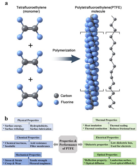
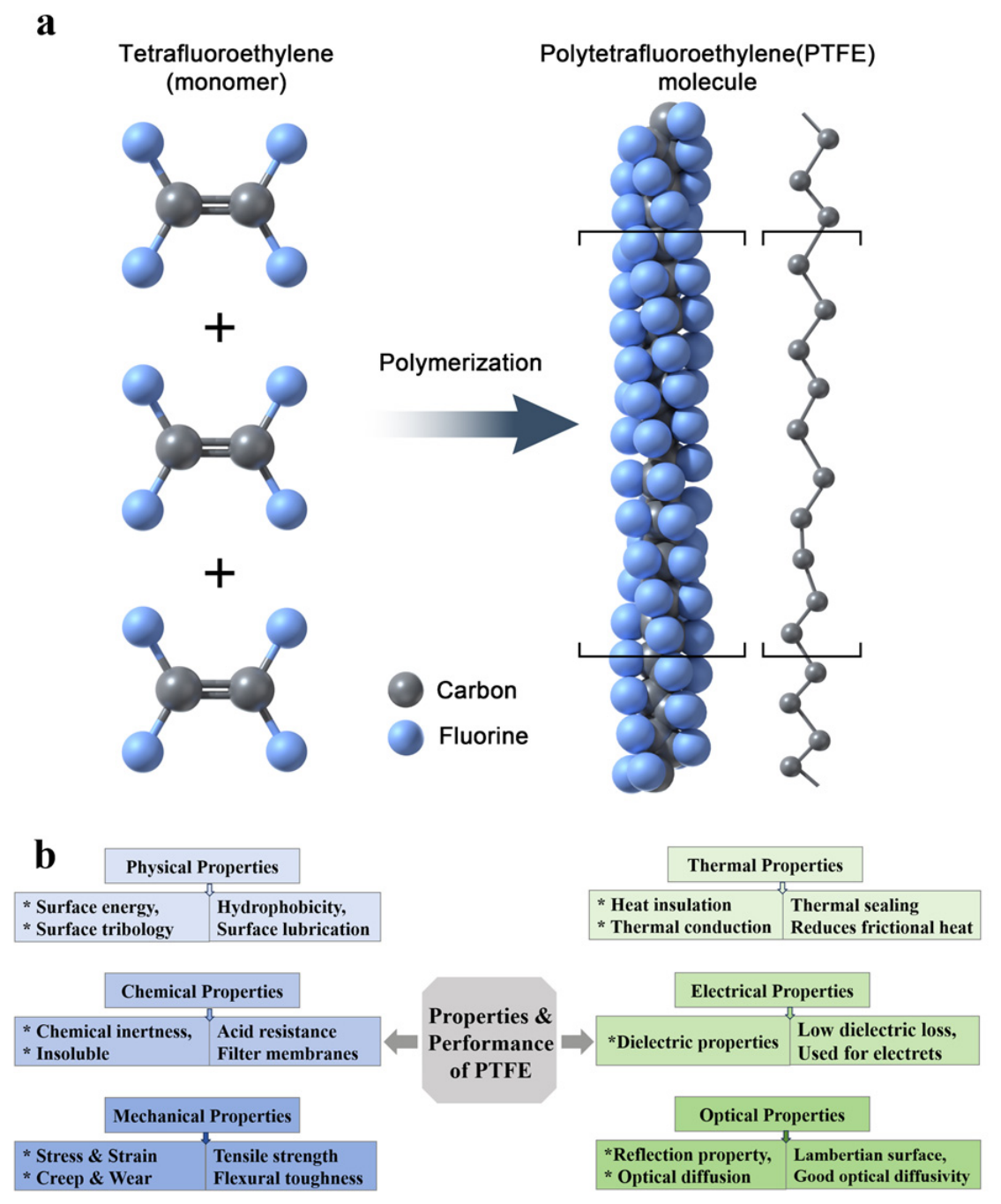
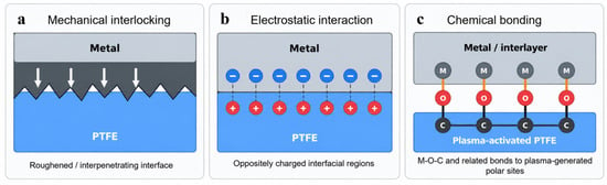
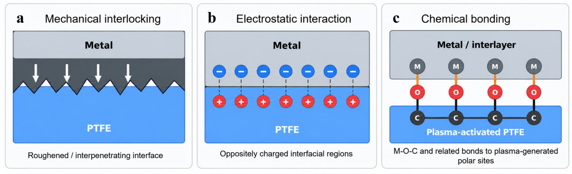
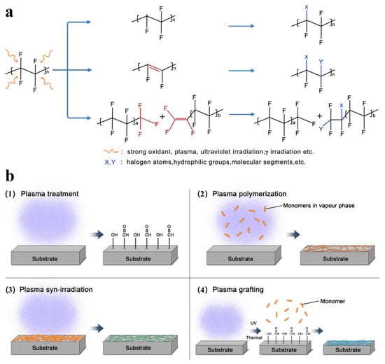
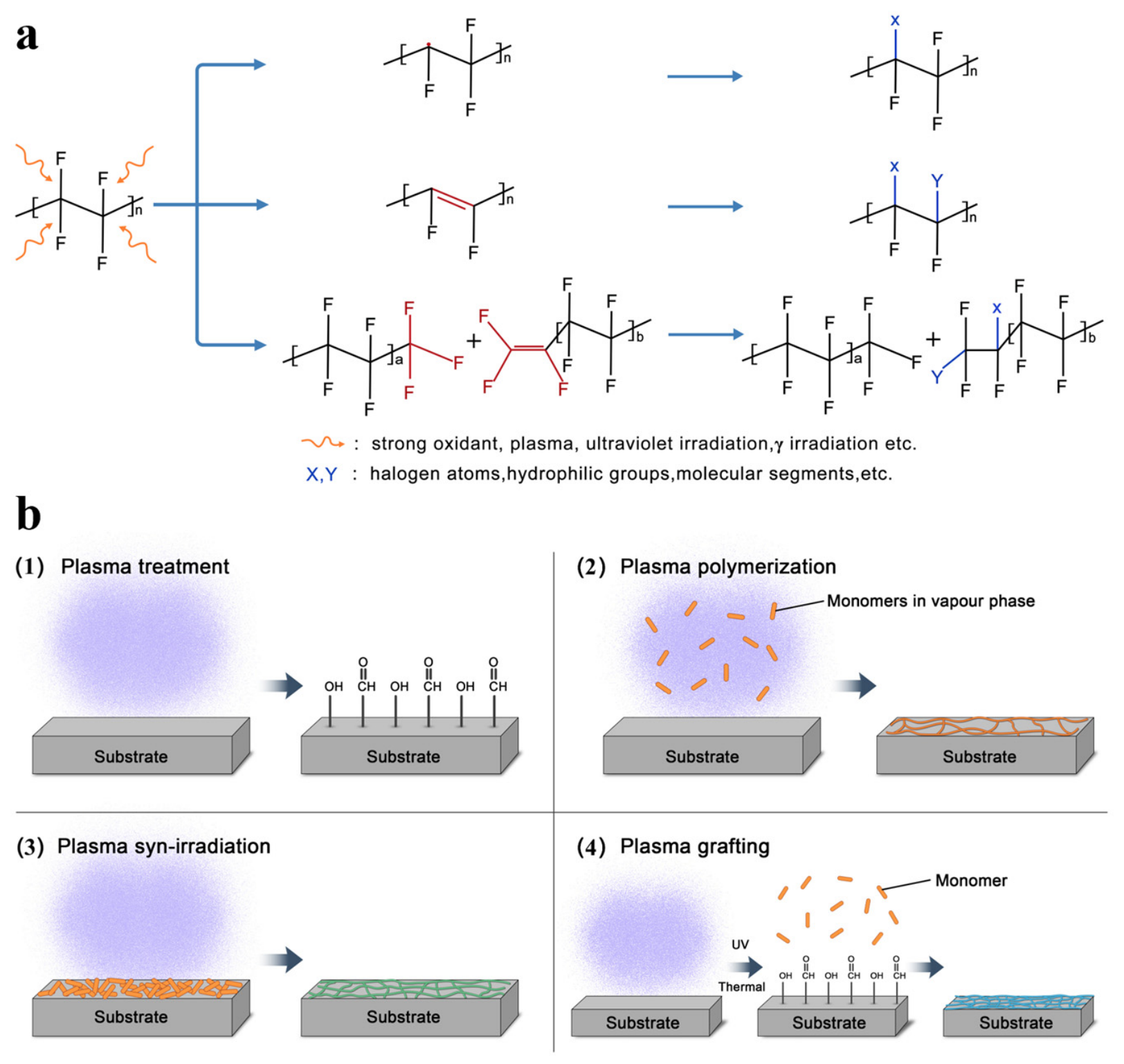
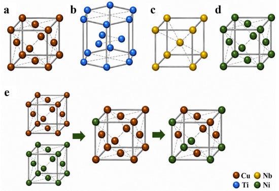
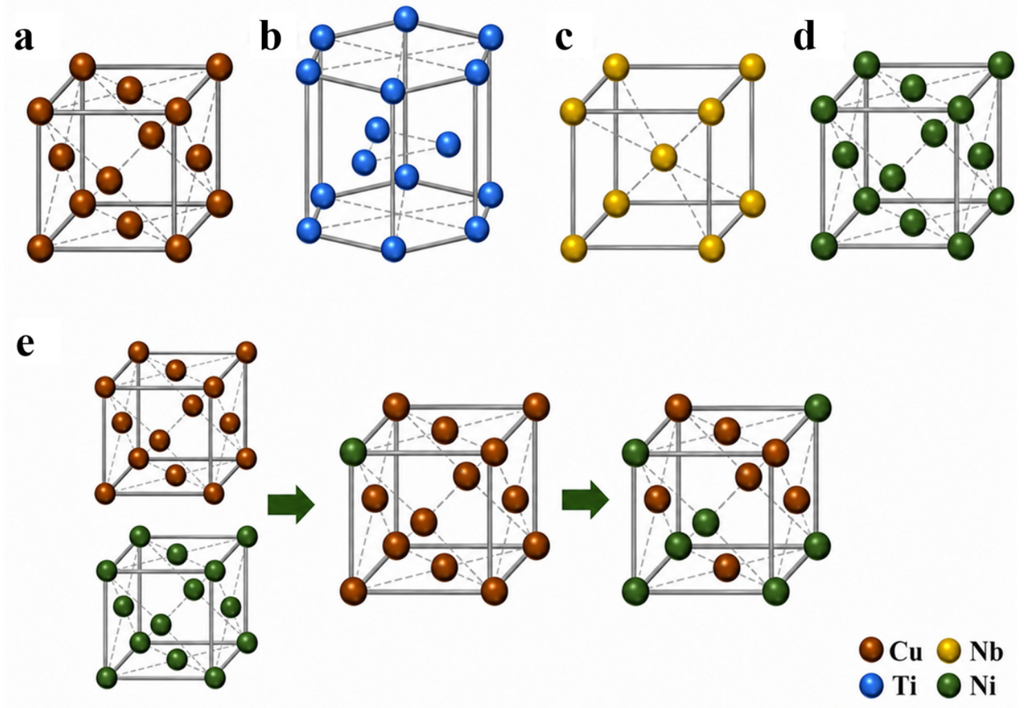
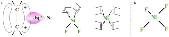

Disclaimer/Publisher’s Note: The statements, opinions and data contained in all publications are solely those of the individual author(s) and contributor(s) and not of MDPI and/or the editor(s). MDPI and/or the editor(s) disclaim responsibility for any injury to people or property resulting from any ideas, methods, instructions or products referred to in the content. |
© 2026 by the authors. Licensee MDPI, Basel, Switzerland. This article is an open access article distributed under the terms and conditions of the Creative Commons Attribution (CC BY) license.