


Abstract
This paper presents an FPGA (Field-Programmable Gate Array) implementation of a low-power VLSI (Very Large-Scale Integration) architecture for medical image scaling in portable diagnostic systems. The proposed architecture employs bilinear interpolation optimized through FSM (Finite-State-Machine)-based control, a clock-enable technique, and selective block activation to reduce switching activity and dynamic power consumption while preserving image quality. The architecture is described in Verilog HDL, synthesized using Vivado 2024.1, and implemented on the Xilinx Zynq-7000-based ZedBoard platform. A controlled post-implementation power analysis on the same FPGA platform demonstrates a reduction in estimated total on-chip power from 3.739 W for the unoptimized baseline architecture to 1.053 W for the optimized architecture, corresponding to an approximately 71.8% reduction. The system supports multiple operational modes, including original image display, grayscale conversion, Sobel X filtering, and Sobel Y filtering, providing enhanced diagnostic flexibility. Quantitative assessment of the exemplary X-ray Image 1 yielded PSNR (Peak Signal-to-Noise Ratio) of 42.97 dB and SSIM (Structural Similarity Index) of 0.9557, demonstrating satisfactory image-quality preservation after scaling. The proposed architecture demonstrates the feasibility of low-power FPGA-based medical image scaling for portable diagnostic and telemedicine imaging systems, offering an effective balance between energy efficiency and image fidelity.
1. Introduction
Medical imaging plays a vital role in modern healthcare by supporting disease diagnosis, treatment planning, image-guided interventions, and telemedicine. Imaging modalities such as X-ray, computed tomography (CT), magnetic resonance imaging (MRI), and ultrasound produce large volumes of image data that must be displayed accurately across a wide range of medical workstations, portable diagnostic devices, and remote healthcare platforms. As healthcare systems increasingly adopt portable and embedded imaging devices, maintaining image quality while adapting images to displays with different spatial resolutions has become an important challenge. Consequently, image scaling has emerged as a fundamental image processing operation for medical visualization, enabling resizing without significantly degrading diagnostically important features [1,2,3,4,5].
The increasing adoption of portable medical imaging systems, point-of-care diagnostics, telemedicine, and embedded healthcare devices has driven demand for real-time image processing solutions that deliver high image quality while minimizing computational complexity and power consumption. FPGA-based hardware accelerators have therefore emerged as attractive platforms because they offer deterministic processing, low latency, and energy-efficient implementation compared with software-based solutions [1].
Image scaling enlarges or reduces an image’s spatial resolution by estimating the intensity values of newly generated pixels using interpolation algorithms. Numerous interpolation techniques have been developed, including nearest-neighbor, bilinear, bicubic, edge-directed, adaptive, and, more recently, learning-based methods [4,6]. Nearest-neighbor interpolation offers very low computational complexity but often introduces blocking artifacts and poor visual quality. Bicubic and adaptive interpolation techniques generally achieve better edge preservation and smoother visual appearance; however, they require substantially higher computational complexity and hardware resources. Bilinear interpolation provides a practical compromise between hardware complexity and image quality, requiring fewer arithmetic operations while producing satisfactory interpolation accuracy. Owing to these advantages, bilinear interpolation remains one of the most suitable techniques for FPGA and VLSI implementations where area, latency, memory utilization, and power consumption are primary design considerations [7,8,9,10,11,12,13,14,15].
The growing demand for portable healthcare equipment and telemedicine systems has significantly increased interest in FPGA-based medical image processing. Compared with software implementations on general-purpose processors, FPGA platforms provide inherent parallelism, deterministic execution, hardware reconfigurability, and efficient utilization of computational resources. These characteristics enable high-performance image processing while meeting the stringent constraints of embedded medical systems. Recent studies have demonstrated FPGA-based implementations for medical image processing, interpolation, and image enhancement using hardware–software co-design, FPGA accelerators, and dedicated image-processing architectures [1,3,6]. Although these approaches improve computational performance, portable medical devices remain constrained by battery capacity, thermal limitations, and available hardware resources. Therefore, reducing power consumption has become as important a design objective as image quality and computational performance [16,17,18,19,20,21,22].
Several FPGA-based image scaling architectures have been reported in the literature [23,24]. Ramadevi and Chari [6] presented an FPGA implementation of an efficient image scaler using a modified area generation technique to improve interpolation performance. Moses et al. [7] comprehensively reviewed VLSI architectures for image interpolation and highlighted the trade-offs between interpolation quality, hardware complexity, and implementation cost. Chen and colleagues proposed several hardware image-scaling architectures, including low-cost image-scaling processors [8], adaptive edge-enhanced image scalers [9], novel interpolation chips [11], adaptive image scalers [12], and edge-oriented VLSI architectures [13], demonstrating significant improvements in interpolation quality and hardware efficiency. Earlier studies, including WinScale [15], FPGA-based bicubic interpolation architectures [17], FPGA implementations of bilinear interpolation [16], and digital image scaling techniques [18], established important foundations for hardware image scaling. Classical investigations of interpolation methods for medical imaging by Lehmann et al. [14], Parekar et al. [19], and Duncan and Ayache [20] further emphasized the importance of preserving image quality during medical image resampling and visualization.
Despite these significant developments, several research challenges remain. Existing FPGA image scaling architectures have predominantly focused on improving interpolation accuracy, increasing processing speed, or reducing hardware complexity. Fewer studies have addressed power optimization as a primary design objective while simultaneously preserving image quality in medical image scaling applications. Furthermore, limited work has integrated finite-state-machine (FSM)-based control, selective activation of computational modules, efficient BRAM utilization, and fixed-point arithmetic within a unified low-power FPGA architecture specifically targeted toward portable medical imaging systems. These limitations motivate the development of hardware architectures that achieve high image quality while reducing power consumption and efficiently utilizing FPGA resources.
To address these challenges, this paper presents a low-power FPGA-based VLSI architecture for medical image scaling using bilinear interpolation. The proposed architecture combines BRAM-based image storage, FSM-controlled processing, selective module activation, and fixed-point arithmetic to reduce switching activity, hardware utilization, and overall power consumption while maintaining high image quality. The complete architecture is implemented in Verilog HDL using Vivado 2024.1 and validated on an Xilinx Zynq-7000 FPGA platform through FPGA resource utilization analysis, post-implementation power estimation, and objective image quality assessment using peak signal-to-noise ratio (PSNR) and structural similarity index measure (SSIM).
The main contributions of this work are summarized as follows:
- (1)
- A low-power FPGA architecture for medical image scaling that integrates BRAM-based image storage, FSM-controlled processing, selective functional activation, and fixed-point bilinear interpolation to reduce hardware complexity and power consumption.
- (2)
- A complete hardware implementation of the proposed architecture using Verilog HDL on an Xilinx Zynq-7000 FPGA with Vivado 2024.1, demonstrating improved energy efficiency while preserving image quality.
- (3)
- Comprehensive experimental validation through FPGA resource utilization, post-implementation power analysis, and objective image quality evaluation using PSNR and SSIM, demonstrating the suitability of the proposed architecture for portable medical imaging and telemedicine applications.
2. Related Work
The advances in image scaling have focused on improving interpolation accuracy, reducing computational complexity, and optimizing hardware implementation for embedded image processing applications. Depending on the interpolation strategy, existing methods can be broadly classified into conventional polynomial-based interpolation techniques and more recent adaptive or learning-based approaches. In parallel, significant research has focused on FPGA and VLSI architectures that enable efficient hardware implementation of these algorithms. This section reviews the major developments and identifies the research gap addressed in this work.
2.1. Image Scaling and Interpolation Techniques
Image interpolation estimates the intensity values of newly generated pixels during image resizing and directly influences the visual quality of the scaled image. Classical interpolation methods include nearest-neighbor, bilinear, and bicubic interpolation, whereas more recent approaches employ adaptive edge-directed and deep learning techniques to improve reconstruction quality [4,14,19]. Nearest-neighbor interpolation offers the lowest computational complexity but often produces blocking artifacts, making it unsuitable for high-quality medical image visualization. Bicubic interpolation generally produces smoother intensity transitions and better edge preservation; however, its higher arithmetic complexity increases hardware costs. Bilinear interpolation provides an effective compromise between computational complexity and interpolation accuracy, making it one of the most widely adopted techniques for FPGA and VLSI implementations [7,8].
Recent developments have introduced learning-based interpolation methods that can produce excellent reconstruction quality for medical images [2,4,5]. Although these methods improve image fidelity, they typically require significantly more computational resources, memory capacity, and power. Consequently, their deployment in portable FPGA-based medical imaging systems remains challenging.
2.2. FPGA-Based Image Scaling Architectures
Numerous FPGA and VLSI architectures have been proposed to improve the hardware efficiency of image scaling algorithms. Ramadevi and Chari [6] presented an FPGA image scaler that employed a modified area-generation technique, reducing computational complexity while maintaining flexible scaling capability. Moses et al. [7] surveyed VLSI interpolation architectures and highlighted the trade-offs between interpolation accuracy, hardware complexity, and implementation cost.
Chen and colleagues proposed several influential image-scaling architectures, including low-cost image-scaling processors [8], adaptive edge-enhanced image scalers [9], interpolation chips [11], adaptive image scalers [12], and edge-oriented VLSI processors [13]. These studies demonstrated significant improvements in interpolation quality while reducing hardware resources through optimized arithmetic operations, efficient buffering strategies, and pipelined architectures. Earlier hardware implementations, including WinScale [15], FPGA-based bilinear interpolation [16], bicubic interpolation architectures [17], and digital image scaling techniques [18], established important design methodologies that continue to influence modern FPGA image scaling systems.
Recent FPGA-based medical image processing architectures have further demonstrated the advantages of hardware acceleration for embedded healthcare applications [1,3]. These studies confirm that FPGA platforms provide high computational throughput and hardware flexibility while supporting the stringent performance requirements of medical imaging systems.
2.3. Research Gap
Although substantial progress has been made in interpolation algorithms and FPGA-based image-scaling architectures, several limitations remain. Most existing research has primarily focused on improving interpolation quality, processing speed, or hardware resource utilization. Comparatively fewer studies have investigated low-power FPGA architectures specifically designed for medical image scaling applications. Furthermore, existing implementations generally consider interpolation optimization independently from power-aware architectural techniques such as FSM-controlled processing, selective functional activation, efficient BRAM utilization, and fixed-point arithmetic. The integration of these techniques within a unified FPGA framework remains limited.
To address these limitations, the proposed work develops a low-power FPGA-based VLSI architecture that combines fixed-point bilinear interpolation, BRAM-based image storage, FSM-controlled processing, and selective activation of computational modules. Unlike previous architectures that primarily emphasize interpolation accuracy or hardware performance, the proposed design targets reduced power consumption, efficient FPGA resource utilization, and preservation of medical image quality, making it well suited for portable diagnostic and telemedicine applications.
3. Bilinear Interpolation and Image Scaling Operations
Image scaling is a fundamental operation in digital image processing that resizes images to match the spatial resolution of different display devices while preserving visual information. In medical imaging applications, image scaling must maintain diagnostically important structures without introducing excessive distortion or computational overhead. The quality of the scaled image largely depends on the interpolation algorithm employed to estimate the intensity values of newly generated pixels. Consequently, the choice of interpolation technique significantly affects image quality, as well as hardware complexity, memory utilization, and power consumption in FPGA-based implementations.
Among the available interpolation methods, nearest-neighbor, bilinear, bicubic, adaptive edge-directed, and, more recently, learning-based techniques have been extensively investigated [4,14,19]. Nearest-neighbor interpolation offers the lowest computational complexity but generally produces blocking artifacts and poor edge continuity. Bicubic and adaptive interpolation methods provide improved edge preservation and smoother visual appearance; however, they require substantially higher arithmetic complexity, memory resources, and hardware cost. Recent deep learning-based interpolation methods further improve reconstruction accuracy but demand considerable computational resources and power, making them less suitable for resource-constrained FPGA implementations [2,4,5].
Bilinear interpolation provides an effective compromise between interpolation accuracy and implementation complexity. It requires only four neighboring pixels and simple arithmetic operations, resulting in lower hardware resource utilization while maintaining satisfactory image quality. Owing to these advantages, bilinear interpolation has been widely adopted in FPGA and VLSI image scaling architectures [6,7,8,9,10,11,12,13,14,15]. Therefore, the present work employs bilinear interpolation as the underlying scaling algorithm and focuses on improving its hardware implementation through low-power architectural optimization rather than modifying the interpolation algorithm itself.
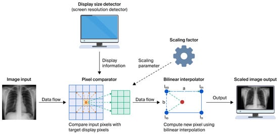
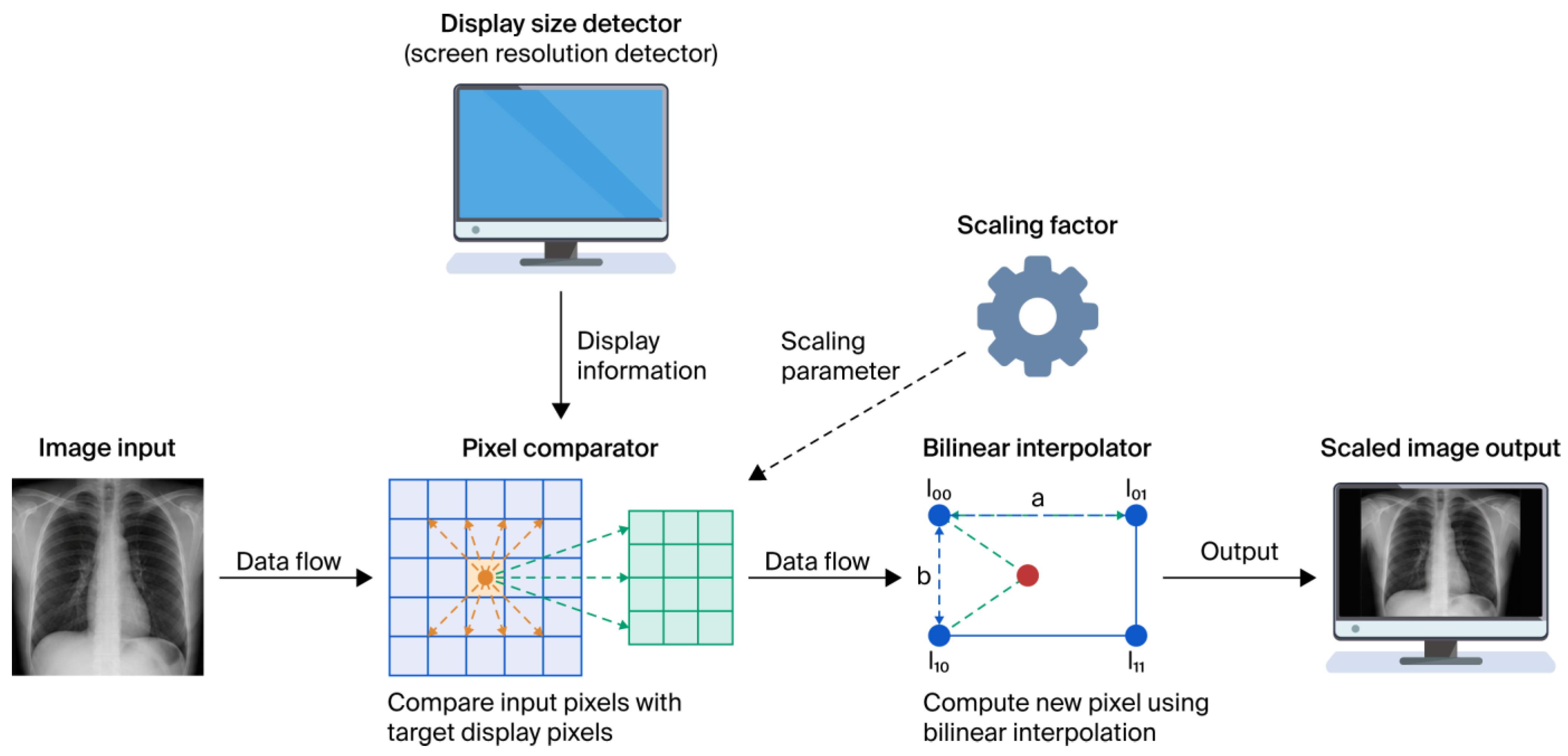
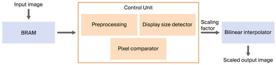
Before describing the mathematical formulation of bilinear interpolation, it is useful to understand the overall image-scaling process adopted in this work. The proposed system first receives the input image dimensions together with the configured target display/image dimensions. Based on these dimensions, the image-to-display ratio is computed, and the required scaling parameters are automatically determined; then, the corresponding neighboring pixels are identified and supplied to the bilinear interpolation stage to estimate the output pixel intensity. The resulting scaled image is then generated for display. In the present FPGA prototype, the VGA interface operates with a fixed 640 × 480 display configuration; therefore, the target resolution information is configured in the hardware rather than dynamically detected from the connected physical display. Figure 1 illustrates the overall system-level image-scaling process adopted in this work.
Figure 1.
System-level processing flow of the proposed medical image scaling approach.
Block diagram functioning:
- Input Image: A medical image will be given as an input to the pixel comparator
- Display Size detector/Screen resolution configuration detector: This block provides the target width and height required by the scaling-control logic. In the present FPGA implementation, these target dimensions are predefined/configured in the hardware rather than dynamically detected from the connected physical display. The target dimensions are supplied to the Pixel Comparator for scaling-factor computation.
- The Pixel Comparator: It will compare the input image dimensions with the configured target dimensions and automatically determine the required scaling factor.
- In this work, the scaling factor is defined as the ratio of the input image dimension to the corresponding target dimension. A scaling factor less than 1 indicates upscaling, whereas a scaling factor greater than 1 indicates downscaling. The interpolator scales the input image to match the target dimensions.
3.1. Bilinear Interpolation Principle
Bilinear interpolation estimates the intensity of an unknown pixel by performing linear interpolation in the horizontal and vertical directions. Consider an interpolation point (x, y) located inside the square formed by four neighboring pixels , , , and . The interpolated pixel intensity is computed as
where
represent the normalized horizontal and vertical distances between the interpolation point and the surrounding pixels.
F(x, y) = (1 − a)(1 − b)F(x1, y1) + a(1 − b)F(x2, y1) + (1 − a) b F(x1, y2) + ab F(x2, y2)
Equation (1) demonstrates that the interpolated intensity is obtained as a weighted combination of the four neighboring pixels, where the contribution of each pixel depends on its relative distance from the interpolation point. The interpolation process can be interpreted as two consecutive one-dimensional interpolation operations:
- Step 1: Linear interpolation is performed along the horizontal direction to obtain two intermediate intensity values.
- Step 2: These intermediate values are subsequently interpolated along the vertical direction to generate the final output pixel.
This two-stage computation provides smooth intensity transitions while requiring only a small number of arithmetic operations, making bilinear interpolation particularly suitable for hardware implementation.
3.2. Hardware Considerations for Bilinear Interpolation
Although the mathematical formulation of bilinear interpolation is straightforward, its efficient realization on FPGA hardware requires careful architectural optimization. The interpolation operation involves multiplications, additions, memory accesses, and coordinate mapping, all of which influence hardware resource utilization, execution latency, and power consumption.
Several FPGA-based image scaling architectures have addressed these challenges using different optimization strategies. Ramadevi and Chari [6] reduced computational complexity through a modified area-generation technique for flexible image scaling. Moses et al. [7] reviewed various VLSI interpolation architectures and highlighted the trade-offs among interpolation quality, hardware complexity, and implementation cost. Chen and colleagues proposed a series of hardware image scalers employing low-cost arithmetic units, adaptive interpolation, edge enhancement, efficient buffering strategies, and pipelined architectures to improve interpolation quality while reducing hardware resources [8,9,10,11,12,13]. Earlier FPGA implementations based on bilinear interpolation [16], bicubic interpolation [17], and area-pixel scaling [15] established practical hardware design methodologies that continue to influence modern FPGA image scaling systems.
Despite these advances, most reported architectures primarily emphasize interpolation quality, processing throughput, or hardware resource optimization. Fewer studies consider power consumption as a primary design objective, particularly for portable medical imaging systems, where battery life and thermal constraints are critical. Furthermore, many implementations optimize individual hardware components without integrating power-aware architectural techniques such as finite-state-machine (FSM)-controlled processing, selective functional activation, efficient BRAM utilization, and fixed-point arithmetic within a unified image scaling framework.
Recent studies have also explored advanced deep learning approaches for medical image interpolation and super-resolution, particularly for CT slice reconstruction using attention-based frameworks, demonstrating significant improvements in reconstruction quality [22]. However, these methods primarily target algorithmic performance and do not address low-power FPGA implementation for medical image scaling. The research has further demonstrated the effectiveness of FPGA-based architectures for real-time image processing applications by integrating hardware-aware optimization techniques with reconfigurable computing platforms. For instance, Munaf et al. developed an FPGA-based low-light image enhancement system using the Retinex algorithm and a coarse-grained reconfigurable architecture (CGRA), achieving real-time processing with low power consumption and efficient hardware resource utilization. Their work highlights the advantages of FPGA platforms for computationally intensive image processing tasks that require high throughput and energy efficiency. However, the primary focus was on image enhancement under low-light conditions rather than low-power medical image scaling. These developments further underscore the need for dedicated FPGA architectures that combine efficient interpolation techniques with power-aware hardware optimization for real-time medical imaging applications [23].
Recent studies have also explored FPGA-based hardware acceleration for medical image processing beyond image scaling [24]. This work focuses on feature extraction and medical image retrieval, highlighting the growing importance of low-power FPGA architectures for medical imaging applications. These developments motivate the need for efficient FPGA-based image-scaling architectures that combine high image quality with reduced hardware resource utilization and power consumption.
3.3. Motivation for the Proposed FPGA Architecture
The observations above indicate that bilinear interpolation remains an attractive solution for FPGA-based medical image scaling, offering a favorable balance between interpolation accuracy and computational complexity. Rather than increasing algorithmic complexity, the present work focuses on optimizing the underlying hardware architecture to improve energy efficiency while maintaining image quality.
Accordingly, the proposed architecture integrates fixed-point bilinear interpolation with BRAM-based image storage, FSM-controlled processing, and selective activation of computational modules to reduce unnecessary switching activity and hardware utilization. These architectural optimizations enable lower power consumption while preserving the image quality required for medical visualization. The complete architecture is implemented on a Xilinx Zynq-7000 FPGA using Verilog HDL and is evaluated through FPGA resource utilization, post-implementation power analysis, and objective image quality metrics, including PSNR and SSIM.
4. An Overview of Power Dissipation
Power is a critical factor influencing the functionality, efficiency, and reliability of any digital system. Effective power management is therefore essential, particularly for FPGA-based architectures used in portable applications.
In general, the total power dissipation in a VLSI system comprises two major components: static and dynamic power. The following are the details for these power dissipation types.
(1) Static power dissipation: Sources of static power dissipation include leakage current or the current drawn continuously from the power supply. It can be given by Equation (2) as follows:
where Istat represents the static (leakage) current and VDD is the supply voltage.
Pstatic = Istat ∗ VDD
(2) Dynamic dissipation: Sources of dynamic power dissipation include transient currents due to switching, charging, and discharging of load capacitance. It can be given by Equation (3) below:
where CL is the effective load capacitance, VDD the supply voltage, and the operating frequency. Activity factor, i.e., the probability that node switching happens from 0 to 1 (α), if it is considered it leads to the following changes in the above Equation (3) mentioned as Equation (4) below:
Pdynamic = CL ∗ VDD2 ∗ f
Pdynamic = CL ∗ VDD2 ∗ f ∗ α
Equation (3) represents the simplified form, while Equation (4) includes the switching activity factor. Thus, minimizing either of CL, VDD, f, or α can directly reduce power consumption in FPGA systems.
4.1. An Overview of Low-Power FPGA Techniques
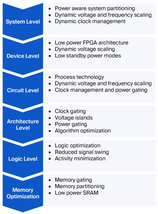
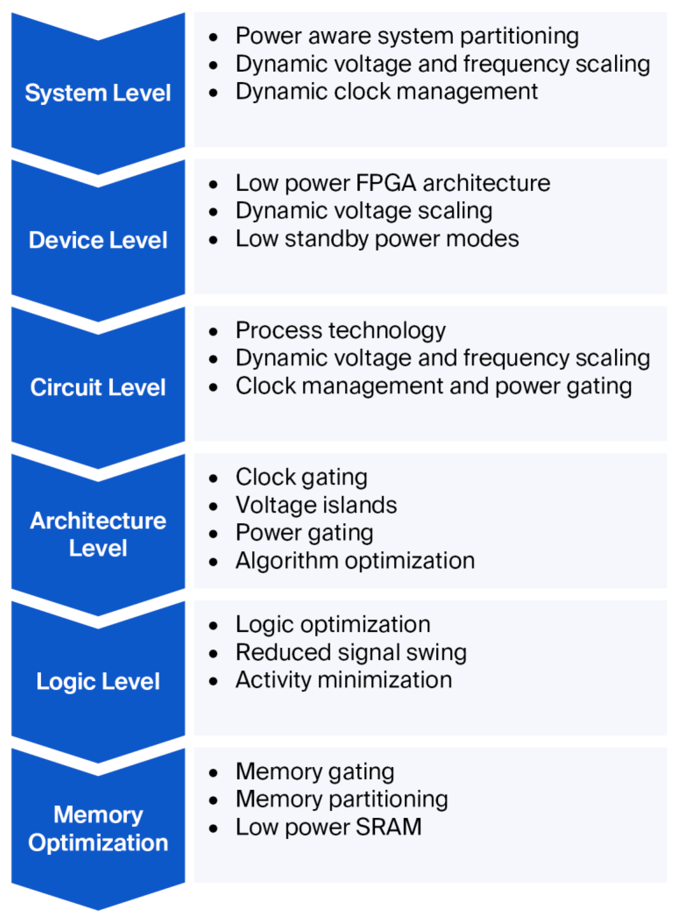
Field-Programmable Gate Arrays (FPGAs) are widely adopted as reconfigurable hardware platforms due to their flexibility, reusability, and rapid prototyping capabilities. However, their high configurability often results in higher power consumption than ASICs. Hence, employing low-power design techniques is crucial for FPGA-based medical and portable imaging systems. The general classification of low-power design techniques for FPGA architectures is illustrated in Figure 2.
Figure 2.
Low-power design techniques.
It presents the hierarchical framework of low-power optimization techniques employed in VLSI and FPGA-based system design. The Figure highlights that power reduction can be achieved at multiple abstraction levels, including the system, device, circuit, architecture, logic, and memory levels. At the system level, techniques such as power-aware partitioning, dynamic voltage and frequency scaling (DVFS), and dynamic clock management improve overall energy efficiency. Device- and circuit-level optimizations focus on reducing active and leakage power through low-power FPGA architectures, process technology improvements, power gating, and efficient clock management. At the architectural and logical levels, methods such as clock gating, voltage islands, algorithm and logic optimization, reduced signal swing, and activity minimization reduce switching activity and computational overhead. Finally, memory optimization techniques, including memory gating, memory partitioning, and low-power SRAM, reduce energy consumption during memory accesses. Although numerous low-power optimization techniques have been reported in the literature, the proposed architecture specifically integrates FSM-controlled processing, fixed-point arithmetic, BRAM-based image storage, and selective functional activation to reduce switching activity during FPGA-based medical image scaling. These techniques are incorporated into the proposed architecture described in Section 5.
4.1.1. Key Low-Power Design Techniques
- Clock Gating:
Selectively disables the clock signal to inactive blocks, thereby preventing unnecessary switching activity and reducing dynamic power.
- Power Gating:
Turns off entire sections of the circuit when idle to minimize leakage power. This technique improves battery life and reduces heat generation, especially in modular FPGA designs.
- Clock and Power Domain Partitioning:
Divides the circuit into independent clock or power domains that can operate at different frequencies or be powered down individually, offering fine-grained control over power consumption.
- Voltage Islands:
Implements multiple voltage domains within the FPGA, allowing high-performance blocks to operate at higher voltages while less critical regions run at lower voltages, thus optimizing overall power efficiency.
- Dynamic Voltage and Frequency Scaling (DVFS):
Adjusts both the supply voltage and clock frequency dynamically based on workload demand. DVFS is widely used in energy-constrained systems such as portable medical devices and IoT applications.
- Minimized Switching Activity:
Reduces unnecessary signal transitions using techniques such as conditional operation and FSM-controlled enable signals, thereby decreasing dynamic power.
- Reduced Swing Logic:
Limits the voltage swing between logic levels to reduce energy per transition, thereby lowering dynamic power consumption.
- Data Retention Strategies:
Utilizes retention flip-flops or low-leakage memory elements that preserve data states during power-down periods, enabling rapid recovery when power is restored.
- Capacitance Reduction:
Minimizes both interconnect and load capacitances through optimized routing and resource sharing, effectively reducing the dynamic power component.
- Sub-Threshold Voltage Operation:
Operates selected blocks below the transistor threshold voltage () to drastically reduce both dynamic and leakage power, albeit with a moderate speed trade-off.
In summary, these techniques collectively contribute to the design of low-power FPGA architectures by targeting both dynamic and static components of total power dissipation. Their strategic combination enables significant power savings while maintaining system performance, making them essential for portable and medical image processing applications.
The above techniques represent general approaches reported in the literature. Among them, the proposed implementation specifically employs FSM-controlled processing, fixed-point arithmetic, BRAM-based image storage, and selective functional activation.
4.1.2. Power Requirements for Image Processing Operations
Image processing operations form the core of many real-time applications, including medical imaging, surveillance, and autonomous systems. However, these operations are computationally intensive and significantly contribute to total power consumption, especially in portable and embedded medical devices where energy efficiency is critical. In FPGA-based implementations, power dissipation depends on both hardware characteristics and algorithmic complexity. Frequent accesses to on-chip Block RAM (BRAM), arithmetic computations performed by adders and multipliers, and switching activity within logic resources constitute the primary sources of dynamic power consumption. Understanding these requirements helps in formulating a low-power architecture for image scaling.
4.1.3. Power Estimation and Optimization in FPGA-Based Image Processing
The major factors influencing power consumption in FPGA-based image processing systems can be categorized into FPGA hardware parameters and algorithmic complexity.
(a) FPGA Parameters
- Core Voltage: Typically ranges from 0.7 V to 1.2 V in modern devices.
- Operating Frequency (f): A higher frequency leads to increased dynamic power.
- Logic Utilization: Greater activity of LUTs, DSP slices, and BRAM raises power.
- I/O Power: Interfaces such as HDMI, VGA, AXI, and DDR consume significant energy.
- Memory Access: Access to external DRAM or on-chip BRAM impacts both static and dynamic power.
(b) Algorithmic Complexity
- Low-power operations: Simple processes like grayscale conversion or thresholding consume less energy.
- High-power operations: Bilinear interpolation, convolution, or segmentation require more arithmetic units and memory access.
- Resolution and Frame Rate: A 1080p @ 60 fps video frame demands considerably more power than a 32 × 32 @ 30 fps image stream.
4.1.4. Power Estimation
The total power can be calculated using Equation (5):
where the dynamic power is obtained using Equation (4) above, in which each parameter contributes to the total energy per frame.
Ptotal = Pstatic + Pdynamic
The reported power consumption values for typical FPGAs vary depending on device family and operating mode. For example, simple thresholding may consume a few hundred milliwatts, while interpolation and filtering can exceed several watts under high-resolution workloads. To address power consumption issues, several power optimization techniques, including clock gating, dynamic voltage and frequency scaling (DVFS), logic partitioning, and selective block activation, have been reported in Figure 2. The proposed architecture specifically adopts FSM-controlled processing, fixed-point arithmetic, BRAM-based image storage, and selective functional activation.
The above discussion provides the theoretical basis for understanding power consumption in FPGA-based image processing systems. Building on these concepts, the following subsection analyzes the proposed low-power image-scaling architecture theoretically and validates it experimentally.
4.2. Theoretical Power Analysis and Experimental Validation for FPGA-Based Image Scaling
Power consumption is a critical design constraint in FPGA-based medical image processing systems, particularly in portable applications where energy efficiency directly affects system performance, thermal management, and battery life. To establish the theoretical foundation of the proposed low-power architecture, this section first discusses power estimation using the classical CMOS dynamic power model. Rather than predicting exact implementation power, the analytical model provides first-order insight into how key design parameters affect dynamic power consumption.
The analytical discussion is subsequently validated using post-implementation power analysis obtained from the Vivado Power Analysis tool.
The proposed FPGA architecture processes a 200 × 200 grayscale medical image stored in on-chip Block RAM and performs bilinear interpolation to generate the scaled output image. Table 1 summarizes the principal parameters used in the analytical discussion.
Table 1.
Image and FPGA Operating Parameters used for Analytical Power Discussion.
The dynamic power consumed by CMOS-based FPGA circuits can be approximated using the well-established expression as follows
where denotes the average switching activity, Ceff is the effective switched capacitance, VDD is the FPGA core supply voltage, and f is the operating clock frequency.
Pdynamic = α CeffVDD2 f
Equation (6) indicates that dynamic power is directly proportional to the switching activity, effective switched capacitance, operating frequency, and the square of the supply voltage. Consequently, reducing unnecessary switching activity is one of the most effective ways to lower power consumption in FPGA implementations.
Unlike ASIC implementations, the effective switched capacitance of an FPGA cannot be directly determined from resource utilization because it depends on proprietary device characteristics, including programmable interconnects, routing capacitances, clock distribution networks, configurable logic blocks, Block RAM resources, and implementation-specific placement and routing. Therefore, analytical power estimation is primarily intended to illustrate the influence of design parameters on power consumption rather than predict the exact implementation power.
Based on Equation (6), dynamic power can be reduced by minimizing one or more of its contributing factors. Since the operating voltage and clock frequency are fixed by the selected FPGA platform, the proposed work primarily focuses on reducing switching activity through hardware-level architectural optimization. The principal optimization techniques incorporated into the proposed FPGA implementation are summarized in Table 2.
Table 2.
Power Optimization Techniques Incorporated in the Proposed FPGA Architecture.
The above optimization techniques collectively reduce unnecessary switching activity, improve hardware utilization, and reduce dynamic power consumption while maintaining the image quality and computational efficiency required for medical image scaling.
The effectiveness of the proposed architecture was verified through hardware implementation on a Xilinx Zynq-7000 ZedBoard using Vivado Design Suite 2024.1. The complete FPGA implementation includes the controller finite-state machine (FSM), fixed-point bilinear interpolation module, Block RAM, VGA display interface, clock generation circuitry, and associated control logic. Table 3 summarizes the estimated total on-chip power reported by the Vivado Power Analysis tool.
Table 3.
Estimated FPGA Power Summary.
The estimated FPGA results confirm that the proposed architectural optimization techniques effectively reduce power consumption while maintaining the computational efficiency required for medical image scaling. Whereas the analytical CMOS power model provides a theoretical understanding of the relationships among switching activity, operating frequency, supply voltage, and effective switched capacitance, the post-implementation Vivado power analysis captures practical implementation effects, including routing resources, clock distribution, Block RAM utilization, controller logic, and I/O circuitry. Consequently, the estimated FPGA results presented in this work provide the primary validation of the proposed low-power architecture, while the analytical discussion provides the theoretical foundation for understanding the factors governing power consumption in FPGA-based image processing systems.
5. Methodology
The overall research methodology adopted in this work is shown in Figure 3. The study begins with the selection of representative medical and benchmark images, followed by the computation of the display-dependent scaling factor. Bilinear interpolation is used as the image scaling algorithm because of its favorable trade-off between computational complexity and interpolation quality. The interpolation algorithm is then implemented using a low-power FPGA architecture incorporating BRAM-based image storage, fixed-point arithmetic, FSM-controlled processing, and selective functional activation. The complete design is described in Verilog HDL and synthesized using Vivado 2024.1 for the Xilinx Zynq-7000 FPGA platform. Finally, the implemented architecture is experimentally evaluated using FPGA resource utilization, post-implementation power analysis, PSNR, and SSIM to validate both hardware efficiency and image quality.
Figure 3.
Architectural Block Diagram.
5.1. Research Workflow
This section presents the workflow adopted to implement the proposed FPGA-based medical image scaling system. The research methodology adopted in this work consists of five sequential stages:
- Identification of the medical image scaling problem for portable FPGA-based systems
- Selection of bilinear interpolation considering computational complexity and image quality
- Development of a low-power FPGA architecture integrating BRAM, FSM control, fixed-point arithmetic, and selective module activation
- Hardware implementation in Verilog HDL using Vivado 2024.1 on the Xilinx Zynq-7000 platform
- Experimental evaluation using image-quality metrics (PSNR and SSIM), FPGA resource utilization, and post-implementation power analysis.
5.2. Proposed Algorithm
The proposed image scaling algorithm integrates bilinear interpolation with low-power design techniques. The algorithmic steps are as follows:
Step 1:
Provide the input medical image and display screen resolution to the Pixel Comparator.
Step 2:
Compute the ratio of image size to display size and derive the scaling factor (S).
Step 3:
Determine the scaling direction:
- Upscaling if S < 1
- Downscaling if S > 1
Step 4:
Feed the computed scaling factor to the Bilinear Interpolator, which performs horizontal and vertical interpolation to generate scaled pixel intensities.
Step 5:
Use FSM-controlled activation to enable only the required modules during interpolation and display, minimizing switching activity and dynamic power consumption.
Step 6:
Output the scaled image through the VGA display interface for subsequent experimental evaluation.
This structured algorithm supports flexible scaling and is optimized for FPGA-based medical imaging platforms.
5.3. Low-Power Architecture
Figure 3 illustrates the proposed low-power FPGA architecture for image scaling. The architecture supports both upscaling and downscaling by computing the appropriate scaling factor and performing bilinear interpolation under FSM-based control.
The proposed architecture scales images by integrating image storage, scaling-factor computation, bilinear interpolation, and display control within an FSM-controlled FPGA. The design supports both upscaling and downscaling and employs the low-power implementation techniques described in Section 4.
The control unit employs an FSM to sequentially activate the Read, Interpolate, and Display stages. Image data are stored in on-chip BRAM and processed using fixed-point bilinear interpolation. Selective module activation minimizes unnecessary switching activity during processing. The scaled image is finally displayed through the VGA interface for visualization.
The proposed architecture reduces switching activity and hardware complexity by selectively activating modules and using fixed-point arithmetic. The following section evaluates its performance experimentally in terms of image quality, FPGA resource utilization, and power consumption.
As illustrated in Figure 3, the architecture consists of an image BRAM, a control unit, a scaling-factor computation module, a bilinear interpolation unit, and a VGA display interface. The input image is stored in on-chip Block RAM (BRAM), from which the address-generation logic accesses neighboring pixels required for bilinear interpolation. The interpolation module performs fixed-point arithmetic using 8-bit pixel values to reduce hardware complexity while maintaining interpolation accuracy. The control unit is implemented as a finite-state machine (FSM) comprising the Idle, Read, Preprocess, Interpolate, and Display states, which sequentially control image retrieval, scaling-factor computation, interpolation, and display. Rather than employing dedicated clock-gating cells, the architecture uses an FSM-controlled clock-enable technique to selectively activate functional modules, thereby reducing unnecessary switching activity and dynamic power consumption. The design directly accesses neighboring pixels from BRAM, minimizing additional memory resources. The interpolated pixel stream is transferred to a VGA controller, which generates the horizontal synchronization (HSYNC), vertical synchronization (VSYNC), and RGB signals for a 640 × 480 display. Timing closure was achieved under the specified design constraints, and synthesis and implementation were performed using the default Vivado timing-driven optimization settings. The proposed hardware architecture emphasizes low resource utilization and power efficiency while preserving image scaling for medical image display applications.
6. FPGA Implementation and Experimental Setup
The proposed FPGA architecture was evaluated through a systematic experimental methodology comprising functional verification, hardware implementation, and quantitative performance assessment. Functional correctness was first verified using RTL simulation, followed by synthesis and implementation on the Xilinx Zynq-7000 (ZedBoard) FPGA using Xilinx Vivado Design Suite 2024.1. The implemented architecture was subsequently evaluated using image-quality metrics (PSNR and SSIM), FPGA resource utilization, and post-implementation power analysis to assess both image fidelity and hardware efficiency.
The hardware design, developed in Verilog HDL, consists of an FSM-controlled processing pipeline comprising image reading from on-chip Block RAM (BRAM), bilinear interpolation, and VGA-based image display. Image data were stored in BRAM and processed using fixed-point arithmetic to reduce hardware complexity and switching activity. The implemented VGA controller displayed the processed output image on a VGA monitor.
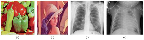
To evaluate the proposed architecture under different image characteristics, we used both standard benchmark images and medical X-ray images. We obtained standard grayscale and color reference images, including Lena and Peppers, from the USC-SIPI Image Database and NYU Sample Image Repository, while representative medical X-ray images were used to assess the proposed architecture’s applicability to medical image processing. Benchmark images of sizes 256 × 256, 512 × 512, and 1024 × 1024 pixels were considered during evaluation. Since the implemented FPGA architecture was designed to process 200 × 200 images stored in on-chip BRAM, higher-resolution images were resized to 200 × 200 before hardware implementation while preserving their visual characteristics. Representative input images used for experimental validation are shown in Figure 4.
Figure 4.
Reference images used for experimental validation. (a) Peppers; (b) Lena; (c) X-ray image 1; (d) X-ray image 2.
The experimental setup is as described in the following paragraph.
We evaluated the performance of the proposed image-scaling architecture using both image-quality and hardware-implementation metrics. We assessed image quality using the Peak Signal-to-Noise Ratio (PSNR) and the Structural Similarity Index (SSIM), computed in MATLAB Online by comparing the scaled output images with their corresponding reference images.
The experimental dataset consisted of four representative images: two benchmark images (Lena and Peppers) and two chest X-ray images, as shown in Figure 4 above. The Lena benchmark image was obtained from the publicly available New York University (NYU) Sample Image Repository, the Peppers benchmark image was obtained from the USC-SIPI Image Database, and the chest X-ray images were obtained from the publicly available NIH ChestX-ray14 dataset. Before FPGA implementation, we resized all images to 200 × 200 pixels, converted them to Xilinx COE format for BRAM initialization, and evaluated them under identical scaling conditions. This work aims to validate the proposed FPGA hardware architecture; therefore, we selected representative benchmark and medical images to verify functional correctness, image-scaling capability, FPGA resource utilization, and power consumption. Figure 4 shows the representative images used for experimental validation. We evaluated hardware implementation performance using Vivado synthesis and implementation reports, including FPGA resource utilization and power consumption. These complementary software- and hardware-based evaluations provide a comprehensive assessment of the proposed FPGA image scaling architecture.
7. Results and Discussion
The proposed FPGA-based medical image scaling architecture was evaluated for image quality, hardware complexity, FPGA resource utilization, and power efficiency. The experimental validation was conducted in two stages. First, the nearest-neighbor, bilinear, and bicubic interpolation techniques were compared using representative benchmark and medical X-ray images to assess reconstruction quality and standalone hardware complexity. Second, the complete FPGA implementation, comprising the bilinear interpolation module, controller FSM, BRAM, VGA interface, and clock management circuitry, was synthesized and analyzed using Xilinx Vivado Design Suite 2024.1. The implementation results were further compared with previously reported FPGA image-scaling architectures to assess the effectiveness of the proposed low-power design.
7.1. Image Quality Evaluation
The image quality of the evaluated interpolation techniques was assessed using the Peak Signal-to-Noise Ratio (PSNR) and Structural Similarity Index Measure (SSIM). Table 4 summarizes the PSNR and SSIM values obtained for a representative medical X-ray image using the nearest-neighbor, bilinear, and bicubic interpolation techniques. For quantitative image-quality evaluation, we used the original images available at the target/higher resolution as reference images, while their 200 × 200 versions were provided as inputs to the FPGA implementation. The scaled pixel data generated by the FPGA were exported as binary output data and subsequently reconstructed as images in MATLAB. PSNR and SSIM were subsequently calculated in MATLAB by comparing the reconstructed FPGA output with the corresponding dimension-matched reference image. For the 200 × 200 to 400 × 400 upscaling experiment, the reconstructed 400 × 400 FPGA output was compared with the corresponding 400 × 400 reference image. We followed the same dimension-matching principle for quantitative evaluation of the scaling results. Thus, the reported PSNR and SSIM values quantify the similarity between the FPGA-generated scaled output and the corresponding reference image at the target resolution.
Table 4.
Quality metrics for exemplary X-ray image 1.
As shown in Table 4, bicubic interpolation achieves the highest reconstruction quality because of its higher-order interpolation model. However, this improvement comes at the cost of increased computational complexity. Bilinear interpolation provides a balanced trade-off between reconstruction quality and hardware implementation complexity, achieving a PSNR of 42.97 dB and an SSIM of 0.9557 for the representative X-ray image while requiring lower computational complexity than bicubic interpolation. This trade-off is also consistent with previous VLSI/FPGA image-scaling studies, where bilinear interpolation has been adopted because of its relatively low computational complexity and favorable hardware implementation characteristics [7]. Considering these image-quality results together with the hardware implementation and estimated power results presented subsequently, we selected bilinear interpolation as the core scaling method for the proposed low-power FPGA architecture. To extend the quantitative validation beyond the representative X-ray image, we evaluated the proposed bilinear interpolation using all four test images shown in Figure 4: Peppers, Lena, X-ray Image 1, and X-ray Image 2. We standardized all images to 200 × 200 pixels before processing. For this quantitative evaluation, all four images were upscaled from 200 × 200 to 400 × 400 pixels. We determined PSNR and SSIM using the dimension-matched reference procedure described above. Table 5 presents the individual results together with the mean and standard deviation across the four test images.
Table 5.
Quantitative image-quality evaluation of the proposed bilinear interpolation across the test images for upscaling.
The results in Table 5 demonstrate that the proposed bilinear interpolation maintains consistent image-quality performance across the four tested images. The PSNR values range from 31.17 to 42.97 dB, while the SSIM values range from 0.9166 to 0.9590. Across the four-image evaluation set, the mean ± sample standard deviation of PSNR is 35.76 ± 5.43 dB, and that of SSIM is 0.9383 ± 0.0221. The variation in the quantitative metrics reflects differences in image content and structural characteristics between the standard benchmark and medical X-ray images. Nevertheless, the consistently high SSIM values indicate preservation of structural information across the evaluated images. These results extend the quantitative validation beyond a single exemplary X-ray image and demonstrate the proposed bilinear implementation’s performance across the defined test set.
7.2. Standalone Interpolation Module Evaluation
Table 6 summarizes the FPGA implementation results of the standalone interpolation modules synthesized independently. The reported hardware resources, maximum operating frequency, and power consumption apply only to the interpolation logic and exclude the controller FSM, BRAM, VGA interface, clock-generation circuitry, and other system-level components. For the standalone interpolation comparison in Table 6, we implemented all three interpolation architectures on the same FPGA device using identical synthesis, implementation, and clock constraints. Post-implementation power analysis was performed in Vivado using the same vectorless/default switching-activity configuration for all three designs; no simulation-derived SAIF/VCD activity files were applied. Under vectorless analysis, Vivado estimates the switching activity of internal nodes from design connectivity, resource functionality, clock constraints, and default input-activity assumptions. Consequently, although the power-analysis configuration was identical for all three implementations, the internally estimated switching activity may differ according to the datapath and logic structure of each architecture. Therefore, the reported standalone power values are implementation-specific Vivado power estimates under a common analysis configuration, rather than an intrinsic algorithm-level power ranking.
Table 6.
FPGA resource utilization and performance of standalone interpolation modules.
All standalone interpolation modules were synthesized and implemented using the same FPGA device (Xilinx Zynq-7000, Advanced Micro Devices, Inc., Santa Clara, CA, USA), Vivado Design Suite 2024.1, identical synthesis and implementation settings, and identical clock constraints. Power estimation was performed using the Vivado Power Analysis tool under the same implementation environment to ensure a consistent comparison among the interpolation techniques. The reported power values, therefore, reflect the implementation characteristics of each interpolation module under comparable design conditions.
The standalone implementation results indicate that bilinear interpolation provides a favorable trade-off among image quality, operating frequency, hardware complexity, and estimated power under the evaluated implementation conditions. Although nearest-neighbor interpolation uses fewer LUTs, the bilinear implementation achieves a maximum operating frequency of 153.1 MHz and an estimated total on-chip power of 0.247 W under the applied Vivado power-analysis configuration. Bicubic interpolation requires greater hardware resources because of its higher arithmetic complexity and also exhibits a higher estimated power value under the same analysis configuration. Since Vivado’s internal switching-activity estimates may differ among the three implemented architectures, the reported power values are implementation-specific estimates rather than an intrinsic power ranking of the interpolation algorithms. Considering the combined image-quality, hardware-resource, frequency, and implementation results, bilinear interpolation was selected as the core scaling method for the proposed FPGA architecture.
7.3. Complete FPGA Architecture Evaluation
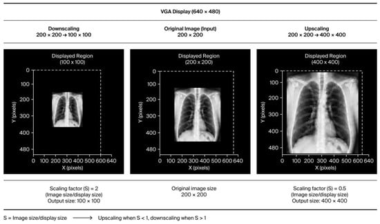
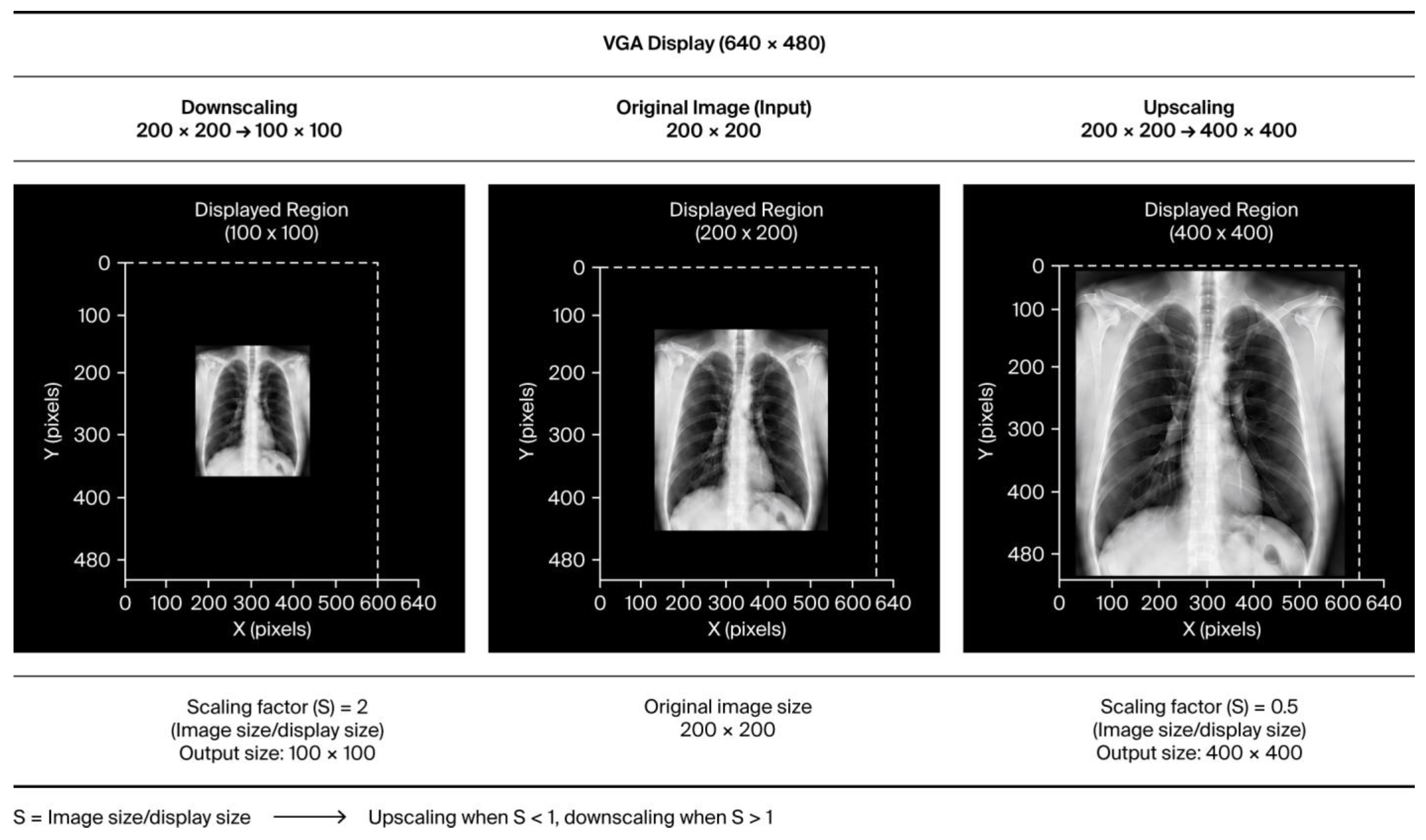
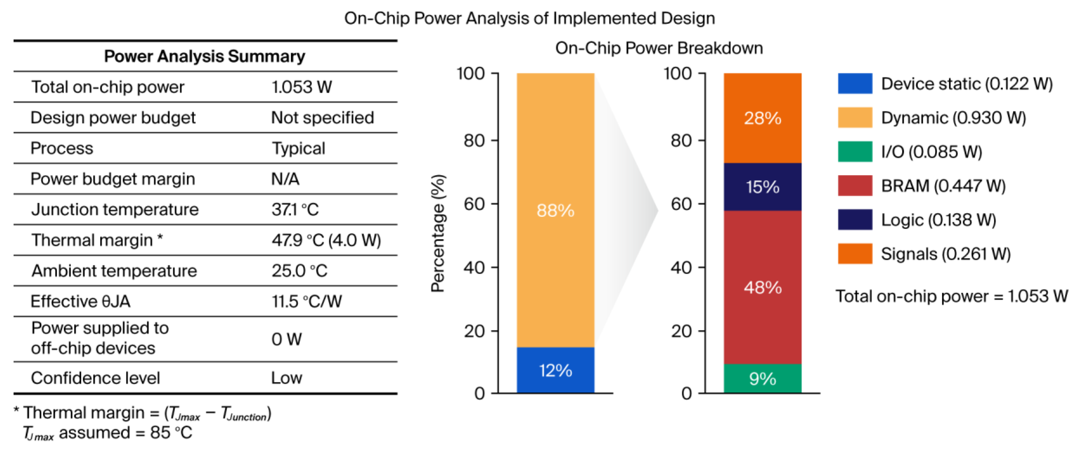
Figure 5 presents a representative input and scaled output image generated by the proposed FPGA architecture, while Figure 6 presents the Vivado post-implementation power analysis of the complete design. The scaled output preserves the overall visual characteristics and intensity transitions of the input image, indicating that the hardware implementation scales the image without introducing noticeable visual distortion. The proposed FPGA implementation successfully generated upscaled and downscaled output images. The upscaling operation increased the image size from 200 × 200 to 400 × 400 pixels with a scaling factor of 0.5. Similarly, the downscaling operation reduced the image size from 200 × 200 to 100 × 100 pixels with a scaling factor of 2. The representative image-quality evaluation in Section 7.1 yields a PSNR of 42.97 dB and an SSIM of 0.9557, demonstrating that the proposed architecture maintains satisfactory image quality while effectively supporting both upscaling and downscaling.
Figure 5.
Representative FPGA image-scaling results using the proposed architecture.
Figure 6.
Vivado post-implementation estimated power analysis report for the complete FPGA architecture.
The standalone bilinear interpolation module consumes 0.247 W, as reported in Table 6. To evaluate the power efficiency of the complete FPGA implementation under controlled conditions, we implemented both unoptimized and optimized versions of the proposed architecture on the same Xilinx Zynq-7000 FPGA using Vivado Design Suite 2024.1, with identical target device, clock constraints, and implementation settings. The complete architecture includes the controller FSM, BRAM-based image storage, VGA interface, clock-generation circuitry, and bilinear interpolation module. To quantify the effectiveness of the proposed low-power optimization techniques under controlled conditions, Table 7 compares the major power components of the complete architecture before and after optimization.
Table 7.
Controlled post-implementation power comparison of the complete proposed architecture before and after low-power optimization.
As shown in Table 7, the Vivado post-implementation estimated total on-chip power decreases from 3.739 W for the unoptimized baseline to 1.053 W for the optimized architecture, corresponding to a reduction of approximately 71.8%. More importantly, the estimated dynamic power decreases from 3.498 W to 0.930 W, representing an approximately 73.4% reduction. The signal, logic, BRAM, and I/O power components also decrease, indicating reduced switching activity after the proposed hardware optimizations. The reported values represent Vivado post-implementation power estimates rather than direct board-level power estimation. Switching activity was estimated using Vivado’s vectorless/default activity estimation; no simulation-derived SAIF or VCD switching-activity file was imported. We evaluated both the unoptimized and optimized implementations using the same power-analysis methodology and implementation conditions to ensure a consistent, controlled comparison. Consistent with the Low confidence level indicated by the Vivado Power Analysis report, the reported values are interpreted as implementation-level power estimates rather than physical power estimations.
To provide a complete assessment of the proposed FPGA implementation, we obtained the resource utilization of the top-level image-scaling architecture from the Vivado synthesis report. Unlike the module-level comparison in Table 6, the results in Table 8 correspond to the complete hardware implementation, including the image display module, the controller FSM, BRAM, the VGA interface, the clock-generation circuitry, and supporting control logic. These results demonstrate that the proposed architecture achieves low hardware resource utilization while maintaining image-scaling performance. Table 8 summarizes the FPGA resource utilization obtained from the Vivado synthesis report for the complete proposed architecture. The resource utilization values reported in Table 8 correspond to the optimized top-level FPGA implementation generated after Vivado synthesis. Table 6 presents the standalone interpolation module results separately. The standalone interpolation module was synthesized independently, whereas the complete architecture was synthesized as an integrated design. During top-level synthesis, Vivado performs logic optimization and removes redundant or unused logic across the entire design, leading to differences in reported resource utilization.
Table 8.
FPGA resource utilization of the complete proposed architecture.
The resource utilization results indicate that the complete architecture requires only 146 slice LUTs and 78 slice registers, together with 23 BRAM tiles and three global clock buffers. This compact use of logic resources is consistent with a fixed-point data path and an FSM-based control strategy. The BRAM utilization is mainly associated with image storage, while the limited register and LUT usage confirm that the proposed architecture is suitable for resource-constrained FPGA-based imaging systems.
7.4. Comparison with Existing FPGA Architectures
Table 9 compares the proposed architecture with previously reported FPGA-based image-scaling architectures in terms of FPGA device, line-buffer requirement, maximum operating frequency, and reported power consumption. Since the compared implementations use different FPGA devices, operating frequencies, image resolutions, and implementation methodologies, the results are presented as a qualitative comparison rather than a direct quantitative ranking. Device-specific logic-resource metrics such as LUTs, slices, and CLBs are excluded from the cross-device comparison because their architectural definitions differ across FPGA families.
Table 9.
Image Scaler architectural performance comparison with existing FPGA implementations.
The reported power value of 4.447 W corresponds to the FPGA implementation reported in Reference [6] and is included only for qualitative comparison with the proposed architecture. The proposed architecture reports an estimated total on-chip power of 1.053 W; however, these values should not be interpreted as a direct power-reduction comparison because the implementations use different FPGA devices and operating conditions. The controlled power-reduction evaluation of the proposed architecture is instead established by the same-device baseline comparison presented in Section 7.3.
Overall, the comparison indicates that the proposed architecture provides a practical balance among operating frequency, display-oriented implementation requirements, and estimated on-chip power. The synthesis results presented in Section 7.3 separately characterize the resource utilization of the proposed Zynq-7000 implementation, while the controlled same-device post-implementation comparison demonstrates the reduction in estimated on-chip power associated with the optimized architecture. These results support the suitability of the proposed design for low-power FPGA-based medical image-scaling applications.
8. Conclusions and Future Scope
This work presented a low-power FPGA-based VLSI architecture for medical image scaling based on bilinear interpolation.
The proposed architecture automatically determines the scaling factor based on the input image and display resolutions, enabling adaptive image resizing without user intervention. To improve energy efficiency, the design incorporates several hardware-level optimization techniques, including clock-enable techniques, selective block activation, fixed-point arithmetic, and an efficient Block RAM (BRAM)-based memory organization. These optimizations effectively reduce switching activity and computational complexity while preserving the processing capability.
The proposed FPGA architecture reduces arithmetic complexity and hardware resource utilization through fixed-point arithmetic, selective block activation, and efficient memory organization while maintaining satisfactory image quality. A controlled post-implementation evaluation on the Xilinx Zynq-7000 FPGA showed that the proposed hardware optimizations reduced the estimated total on-chip power from 3.739 W for the unoptimized baseline architecture to 1.053 W for the optimized implementation, corresponding to an approximately 71.8% reduction, while maintaining a PSNR of 42.97 dB and an SSIM of 0.9557 for the exemplary X-ray Image 1. The complete implementation, including the controller FSM, interpolation module, BRAM, VGA interface, and clock-generation circuitry, confirms the suitability of the proposed architecture for low-power medical image processing applications. Furthermore, the qualitative comparison with existing FPGA image-scaling architectures indicates competitive hardware performance and comparatively low reported on-chip power consumption. These experimental findings validate the effectiveness of the proposed architecture in balancing image quality, FPGA resource utilization, and power consumption, making it suitable for portable and embedded medical imaging applications.
Future work will focus on extending the proposed architecture to support adaptive image scaling for heterogeneous medical display platforms and telemedicine applications. Automatic display-resolution acquisition using Extended Display Identification Data (EDID) through the Display Data Channel (DDC) will also be investigated, enabling the target resolution to be obtained dynamically before scaling-factor computation. Region-of-interest (ROI)-aware image scaling and intelligent display adaptation techniques will be investigated to preserve diagnostically important image regions while improving computational efficiency. In addition, future research will explore advanced FPGA optimization techniques, including improved memory organization, dataflow scheduling, and AI-assisted image enhancement methods to further improve power efficiency and image quality.
Author Contributions
Article writing was done by M.J.-P. under the supervision of P.S. All authors have read and agreed to the published version of the manuscript.
Funding
This research received no external funding.
Data Availability Statement
The benchmark images used in this work are publicly available from the NYU Sample Image Repository https://eeweb.engineering.nyu.edu/~yao/EL5123/SampleData.html, accessed on 16 August 2026, and the USC-SIPI Image Database https://sipi.usc.edu/database/, accessed on 16 August 2026. The chest X-ray images were obtained from the publicly available NIH ChestX-ray14 dataset https://nihcc.app.box.com/v/ChestXray-NIHCC/folder/37178474737, accessed on 16 August 2026.
Acknowledgments
During the preparation of this manuscript/study, the author(s) used Gen AI, such as ChatGPT Plus (OpenAI) and Grammarly Plus, for the purposes of rephrasing statements, language enhancement, and overall presentation improvement. The authors have reviewed and edited the output and take full responsibility for the content of this publication.
Conflicts of Interest
The authors declare no conflicts of interest.
References
- Yadav, A.; Gupta, V.K.; Kumar, B. FPGA-Based Medical Image Processing Using Hardware–Software Co-Design Approach. IEEE Trans. Biomed. Circuits Syst. 2026, 20, 57–68. [Google Scholar] [CrossRef] [Scilit]
- Midde, V.S.; Jayakumar, E.P. Low-Cost Low-Power Approximated VLSI Architecture for High-Quality Image Scaling in Mobile Devices. J. Real.-Time Image Process. 2023, 20, 11. [Google Scholar] [CrossRef] [Scilit]
- Nagornov, N.N.; Lyakhov, P.A.; Valueva, M.V.; Bergerman, M.V. RNS-Based FPGA Accelerators for High-Quality 3D Medical Image Wavelet Processing Using Scaled Filter Coefficients. IEEE Access 2022, 10, 19215–19231. [Google Scholar] [CrossRef] [Scilit]
- Ji, J.; Zhong, B.; Ma, K.-K. Image Interpolation Using Multi-Scale Attention-Aware Inception Network. IEEE Trans. Image Process. 2020, 30, 9413–9428. [Google Scholar] [CrossRef] [Scilit]
- Han, Y.; Sunwoo, L.; Ye, J.C. K-Space Deep Learning for Accelerated MRI. IEEE Trans. Med. Imaging 2020, 39, 377–386. [Google Scholar] [CrossRef] [Scilit]
- Ramadevi, V.; Chari, M.K. FPGA Realization of an Efficient Image Scaler with Modified Area Generation Technique. Multimed. Tools Appl. 2019, 78, 23707–23731. [Google Scholar] [CrossRef] [Scilit]
- Moses, C.J.; Selvathi, D.; Sophia, V.M.A. VLSI Architectures for Image Interpolation: A Survey. VLSI Des. 2014, 2014, 872501. [Google Scholar] [CrossRef] [Scilit]
- Chen, S.-L. VLSI Implementation of a Low-Cost High-Quality Image Scaling Processor. IEEE Trans. Circuits Syst. II Express Briefs 2013, 60, 31–35. [Google Scholar] [CrossRef] [Scilit]
- Chen, S.-L. VLSI Implementation of an Adaptive Edge-Enhanced Image Scaler for Real-Time Multimedia Applications. IEEE Trans. Circuits Syst. Video Technol. 2013, 23, 1510–1522. [Google Scholar] [CrossRef] [Scilit]
- Pang, Z.-Y.; Hong, Z.-T.; Chen, D.-H. An Improved Low-Cost Adaptive Bicubic Interpolation Arithmetic and VLSI Implementation. Acta Autom. Sin. 2013, 39, 407–413. [Google Scholar] [CrossRef] [Scilit]
- Huang, C.-C.; Chen, P.-Y.; Ching, H.-M. A Novel Interpolation Chip for Real-Time Multimedia Applications. IEEE Trans. Circuits Syst. Video Technol. 2012, 22, 1512–1525. [Google Scholar] [CrossRef] [Scilit]
- Chen, S.-L.; Huang, H.-Y.; Luo, C.-H. A Low-Cost High-Quality Adaptive Scaler for Real-Time Multimedia Applications. IEEE Trans. Circuits Syst. Video Technol. 2011, 21, 1600–1611. [Google Scholar] [CrossRef] [Scilit]
- Chen, P.-Y.; Lien, C.-Y.; Lu, C.-P. VLSI Implementation of an Edge-Oriented Image Scaling Processor. IEEE Trans. Very Large Scale Integr. VLSI Syst. 2009, 17, 1275–1284. [Google Scholar] [CrossRef] [Scilit]
- Lehmann, T.M.; Gönner, C.; Spitzer, K. Survey: Interpolation Methods in Medical Image Processing. IEEE Trans. Med. Imaging 1999, 18, 1049–1075. [Google Scholar] [CrossRef] [Scilit]
- Kim, C.-H.; Seong, S.-M.; Lee, J.-A.; Kim, L.-S. WinScale: An Image-Scaling Algorithm Using an Area Pixel Model. IEEE Trans. Circuits Syst. Video Technol. 2003, 13, 549–553. [Google Scholar] [CrossRef] [Scilit]
- Gribbon, K.T.; Johnston, C.T.; Bailey, D.G. A Real-Time FPGA Implementation of a Barrel Distortion Correction Algorithm with Bilinear Interpolation. In Proceedings of the Image and Vision Computing, Palmerston North, New Zealand, 26–28 November 2003; Massey University: Palmerston North, New Zealand, 2003; pp. 408–413. [Google Scholar]
- Nuno-Maganda, M.A.; Arias-Estrada, M.O. Real-Time FPGA-Based Architecture for Bicubic Interpolation: An Application for Digital Image Scaling. In Proceedings of the IEEE International Conference on Reconfigurable Computing and FPGAs, Puebla, Mexico, 28–30 September 2005; pp. 8–11. [Google Scholar]
- Andreadis, J.; Amanatiadis, A. Digital Image Scaling. In Proceedings of the IEEE Instrumentation and Measurement Technology Conference, Ottawa, ON, Canada, 16–19 May 2005; pp. 2028–2032. [Google Scholar]
- Parekar, J.A.; Kenyon, R.V.; Troxel, D.E. Comparison of Interpolation Methods for Image Resampling. IEEE Trans. Med. Imaging 1983, 2, 31–39. [Google Scholar] [CrossRef] [Scilit]
- Duncan, J.S.; Ayache, N. Medical Image Analysis: Progress over Two Decades and the Challenges Ahead. IEEE Trans. Pattern Anal. Mach. Intell. 2000, 22, 85–106. [Google Scholar] [CrossRef] [Scilit]
- Sowmya, N.; Rout, S.S.; Patjoshi, R.K. VLSI Implementation in Biomedical Applications: A Review. Int. J. Comput. Inf. Syst. Ind. Manag. Appl. 2020, 12, 155–167. [Google Scholar]
- Uhm, K.-H.; Cho, H.; Hong, S.-H.; Jung, S.-W. An Anisotropic Cross-View Texture Transfer with Multi-Reference Non-Local Attention for CT Slice Interpolation. IEEE Trans. Med. Imaging 2026, 45, 336–349. [Google Scholar] [CrossRef] [Scilit]
- Munaf, S.; Bharathi, A.; Jayanthi, A.N. FPGA-Based Low-Light Image Enhancement Using Retinex Algorithm and Coarse-Grained Reconfigurable Architecture. Sci. Rep. 2024, 14, 28770. [Google Scholar] [CrossRef] [Scilit]
- Samantaray, A.K.; Sahoo, S.; Rahulkar, A.D. FPGA Implementation of AIQ-Based Daubechies Filter Bank for Medical Image Retrieval. In Proceedings of the 2024 IEEE 1st International Conference on Advances in Signal Processing, Power, Communication, and Computing (ASPCC), Bhubaneswar, India, 19–21 December 2024. [Google Scholar]

Disclaimer/Publisher’s Note: The statements, opinions and data contained in all publications are solely those of the individual author(s) and contributor(s) and not of MDPI and/or the editor(s). MDPI and/or the editor(s) disclaim responsibility for any injury to people or property resulting from any ideas, methods, instructions or products referred to in the content. |
© 2026 by the authors. Licensee MDPI, Basel, Switzerland. This article is an open access article distributed under the terms and conditions of the Creative Commons Attribution (CC BY) license.