


Abstract
The crystallization quality of a perovskite active layer is highly sensitive to processing conditions and plays a decisive role in determining the performance of perovskite solar cells (PSCs). Herein, we systematically investigate the synergistic effects of the antisolvent dripping time and annealing time on the active layer crystallization and device performance. By optimizing the chlorobenzene (CB) dripping time during spin coating, we find that the film prepared at 19 s exhibits the most compact and uniform morphology, together with enhanced crystallinity. On this basis, further optimization of post-annealing at 100 °C reveals that 30 min is most favorable for promoting grain growth and minimizing defect formation. As a result, the optimized device delivers a champion PCE of 24.43%, with a short-circuit density (Jsc) of 25.69 mA cm−2, a Voc of 1.14 V, and an FF of 83.20%. This work highlights the critical role of process-window engineering in governing perovskite crystallization and provides an effective route toward high-efficiency PSCs.
1. Introduction
Organic–inorganic halide perovskite solar cells (PSCs) have attracted extensive attention in recent years due to the excellent photophysical properties of perovskites, such as a high absorption coefficient, tunable bandgap, and solution processability [1,2,3,4]. The photovoltaic (PV) performance of PSCs is closely related to the quality of the perovskite active layer. Therefore, many efforts have been devoted to regulating the film formation process to obtain high-quality perovskite films. Among the various fabrication strategies, antisolvent engineering and thermal annealing are regarded as effective ways to regulate the nucleation and crystallization kinetics of a perovskite active layer.
In the film formation process of perovskites, both the antisolvent dripping time and annealing time play critical roles in regulating crystallization kinetics and final film quality. The dripping time of the antisolvent directly affects solvent extraction, intermediate-phase formation, precursor supersaturation, and subsequent nucleation and grain growth [5,6]. Meanwhile, the annealing time further determines the removal of residual solvents, the conversion of intermediate phases, crystal growth, and defect evolution [7,8]. Therefore, proper control of both antisolvent dripping time and annealing time is essential for obtaining dense perovskite films with large grains, high crystallinity, and low trap density. While previous studies have separately investigated antisolvent treatment or annealing conditions, researchers still rely heavily on empirical screening. Taylor et al. proposed a general antisolvent strategy, demonstrating that the role of antisolvents is to regulate nucleation kinetics, with dripping timing being more critical than antisolvent type [5]. However, their work did not systematically investigate the effect of subtle variations in dripping time on film quality. Chang et al. studied the effect of annealing temperature on vapor-deposited MAPbI3 but did not address antisolvent processing [9]. The combined influence of these two processing parameters on perovskite film formation has not been systematically compared within a consistent experimental framework [5,8,9]. This knowledge gap motivates the need for the systematic optimization of both parameters under identical conditions.
In this work, we systematically investigate the influence of antisolvent dripping time (17, 19, and 21 s) and annealing time (20, 30, and 40 min) on the quality of a perovskite active layer and the performance of PSCs. By meticulously studying the crystallization morphology, optical properties, and defect characteristics of perovskite films under different process conditions, the optimal antisolvent dripping time and annealing time are determined. Finally, due to the employment of proper process regulation, the perovskite films exhibited an improved morphology, enhanced crystallinity, and reduced defect density and delivered an improved power conversion efficiency (PCE) of 24.43%.
2. Experimental Section
Materials: FTO glass substrates (sheet resistance = 15 Ω sq−1, thickness = 1.6 mm), lead iodide (PbI2, 99.99%), and methylammonium iodide (MAI, 99.9%) were purchased from Advanced Election Technology Co., Ltd in China. Athocuproine (BCP, >98%) and Formamidinium iodide (FAI, 99.5%) were purchased from Greatcell solar Materials Pty Ltd in China. Phenyl-C61-butyric acid methyl ester (PCBM, 99%) was purchased from Xi’an Polymer Light Technology in China. Cesium iodide (CsI, 99.9%) and (4-(3,6-dimethyl-9H-carbazole-9-yl) butyl)phosphonic acid (Me-4PACz, 99%) were purchased from Shanghai Macklin Biochemical Technology Co., Ltd in China. Chlorobenzene (CB, 99.99%, anhydrous), N, N-dimethylformamide (DMF, >99.9%, anhydrous), and dimethylsulfoxide (DMSO, >99.8%, anhydrous) were purchased from Sigma Aldrich in USA. All chemicals were used without further purification.
Devices Fabrication: FTO glass substrates were cleaned by deionized water, acetone, ethanol, and isopropyl alcohol for 15 min in each step. After being dried by dry nitrogen, the FTO was treated by ultraviolet ozone (UV-O3) for 20 min. The Me-4PACz (0.5 mg/mL in ethyl alcohol and DMF solution (volume ratio 4:1)) was spin-coated on the FTO at 4000 rpm for 30 s and then annealed at 100 °C for 10 min. Then, the perovskite precursor solutions (1.60 M, FA0.85MA0.10Cs0.05PbI3) were spin-coated on the Me-4PACz substrates at 1000 rpm for 6 s and 5000 rpm for 26 s. Then, 200 μL CB was dropped on the perovskite film at 14 s before the end of the program and then annealed at 100 °C for 30 min. Then, PEABr solutions (1 mg in 1 mL IPA and 5 μL DMSO solution) were spin-coated at 4000 rpm for 35 s and annealed at 100 °C for 30 min. Then, PCBM solutions (20 mg/mL in CB) were spin-coated at 4000 rpm for 30 s and the BCP was deposited onto the substrates at 4000 rpm for 30 s. Finally, 100 nm of Ag electrode was thermally evaporated under high-vacuum (less than 2.8 × 10⁻⁴ Pa).
Characterization: XRD patterns were collected using Cu-Kα radiation (Rigaku SmartLab, Japan). The UV–vis spectra of the perovskite films were measured using UV-Vis-NIR spectrophotometer (Shimadzu UV-3600, Japan). SEM images were obtained by a field-emission scanning electron microscope (Thermo scientific Apreo C, USA). PL was employed by a micro-Raman spectrometer (Renishaw in Via, England) with an excitation laser wavelength of 532 nm. J-V characteristics were measured by a Keithley 2450 source meter under one sun illumination (AM 1.5 G, 100 mW cm−2) using a solar simulator (Newport LCS-100, China) equipped with a 100 W Xenon ARC lamp (Newport 6252, China), in which the light intensity was calibrated by an NREL-calibrated Si solar cell equipped with a KG-2 filter. SCLC and dark J-V characteristics were measured by a Keithley 2450 source meter (China) in the dark.
3. Results and Discussion
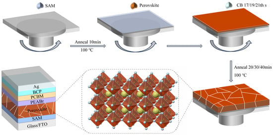
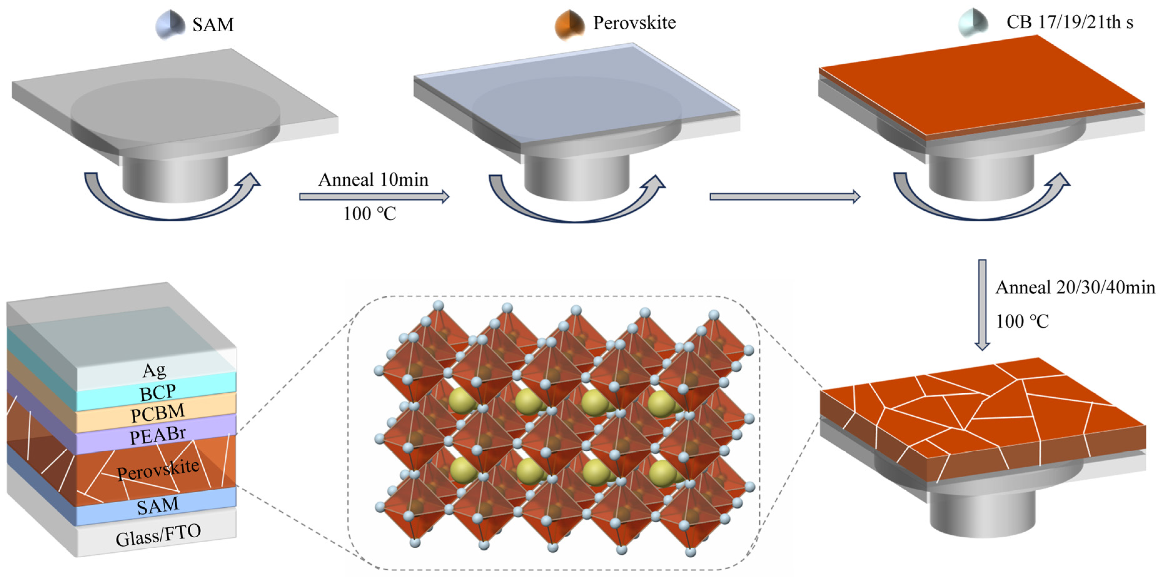
As shown in Figure 1, to systematically clarify the effects of the antisolvent dripping time and annealing time on perovskite film formation, we first optimized the antisolvent dripping time by dropping 200 μL of chlorobenzene (CB) at different times before the end of spin coating. Previous studies on closely related FAMACs perovskite systems have reported optimal dripping times of approximately 19–20 s [10,11,12]. Accordingly, we selected 19 s as the central point and examined two adjacent time points (17 and 21 s) with 2 s increments, and the films were subsequently annealed at 100 °C for 30 min [13,14,15]. Based on the resulting film formation quality, the optimal CB dripping time was selected for further study. The annealing window was first narrowed down by steady-state photoluminescence (PL) measurements at 20, 25, and 30 min (5 min intervals). The PL intensity at 25 min fell between those at 20 and 30 min, suggesting suboptimal film quality and justifying its exclusion from subsequent optimization (Figure S1, Supplementary Materials). The annealing time was further tuned at 100 °C for 20, 30, and 40 min under the optimized antisolvent dripping condition. Finally, the suitable annealing time was also selected based on the quality of the active layer and PV parameters. More experimental details are presented in the Section 2.
Figure 1.
Schematic illustration of the overall research process for optimizing the antisolvent dripping time and annealing time during perovskite film formation.
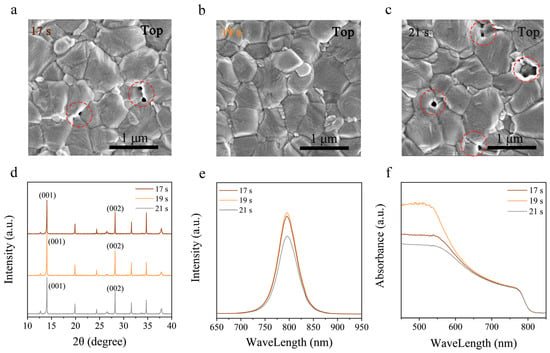
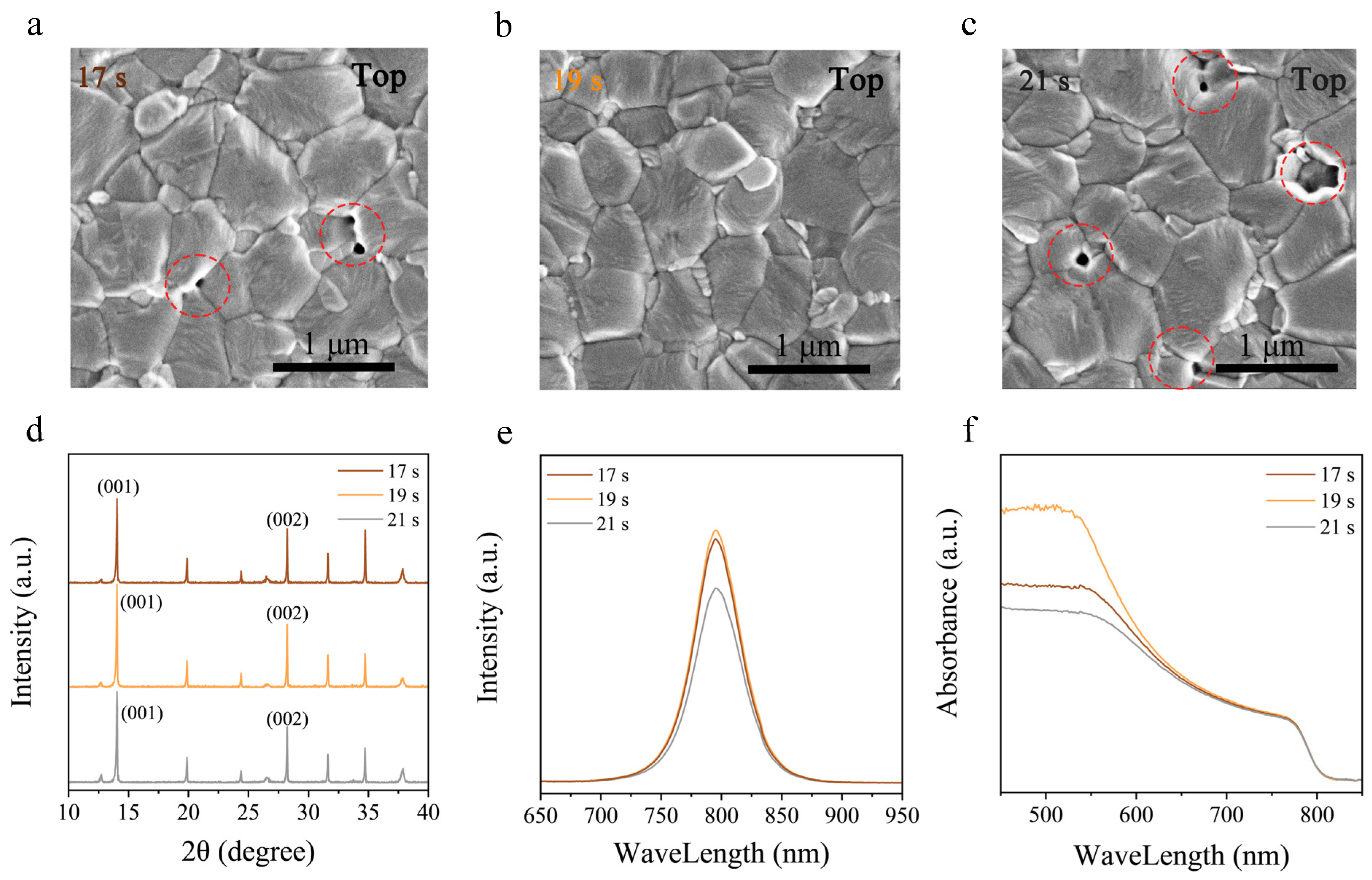
A scanning electron microscope (SEM) was employed to evaluate the influence of the antisolvent dripping time on the morphology of the perovskite film. As shown in Figure 2a, when the CB was dropped at 17 s, the obtained perovskite film exhibited relatively poor film quality, with an inhomogeneous surface and a few visible voids. This result indicates that the antisolvent was introduced at a relatively early stage, thereby resulting in a state where the film has already formed, while its microstructure remains insufficiently optimized [15]. In contrast, the perovskite film prepared with CB dripping at 19 s (Figure 2b) showed the best morphology among all the samples. The film presented a dense, uniform, and smooth surface without obvious morphological defects, indicating a more suitable kinetic window for balanced solvent extraction and crystal growth and thus contributing to the formation of a high-quality perovskite film [16,17]. However, when the CB dripping time was further delayed to 21 s, the film morphology became worse again, as shown in Figure 2c. Increased voids and cracks were observed, stemming from delayed antisolvent addition. To be more specific, once the wet films had already undergone substantial spontaneous solvent evaporation and even partial crystallization in some local regions, the subsequent introduction of the antisolvent could no longer effectively regulate nucleation and uniform solidification [5]. Interestingly, it seems that the antisolvent dropping time does not have an obvious effect on the grain size.
Figure 2.
(a–c) SEM images, XRD patterns (d), PL spectra, (e) and UV-vis spectra (f) of perovskite films prepared at varying antisolvent dropping times of 17, 19, and 21 s, respectively.
Moreover, X-ray diffraction (XRD) measurements were carried out to further clarify the effect of the antisolvent dripping time on perovskite crystallization. As shown in Figure 2d, all the films exhibited similar characteristic diffraction peaks of the perovskite phase, suggesting that variation in the CB dripping time does not alter the basic crystal structure of the perovskite films. However, the crystallization quality is strongly dependent on the dripping time of CB. Both films prepared at 17 and 21 s exhibited weaker (001) peaks, indicating relatively poor crystallinity. In contrast, the film prepared at 19 s showed the highest diffraction intensity of (001) peak, revealing improved crystallinity and more favorable crystal growth orientation [18,19]. To quantitatively evaluate the crystallinity, the integrated intensity of the (001) peak was calculated for each condition (Figure S2, Supplementary Materials), with intensity ratios of I19s/I17s = 1.25, and I21s/I17s = 1.12, further confirming the optimal crystallinity at 19 s. Therefore, 19 s CB dripping facilitates the formation of high-quality perovskite active layers with boosted crystallinity and favorable crystal orientation. In addition, the perovskite films prepared with a fixed CB dripping time of 19 s exhibited a higher photoluminescence (PL) intensity (Figure 2e) and stronger light absorption intensity (Figure 2f), indicating reduced non-radiative recombination due to the enhanced crystallization quality of the perovskite layer [20]. In summary, all the above results are in good agreement with the SEM observations, collectively demonstrating that 19 s is the optimal antisolvent dripping time.
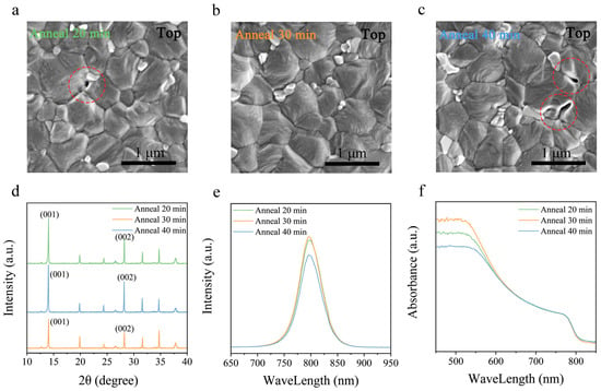
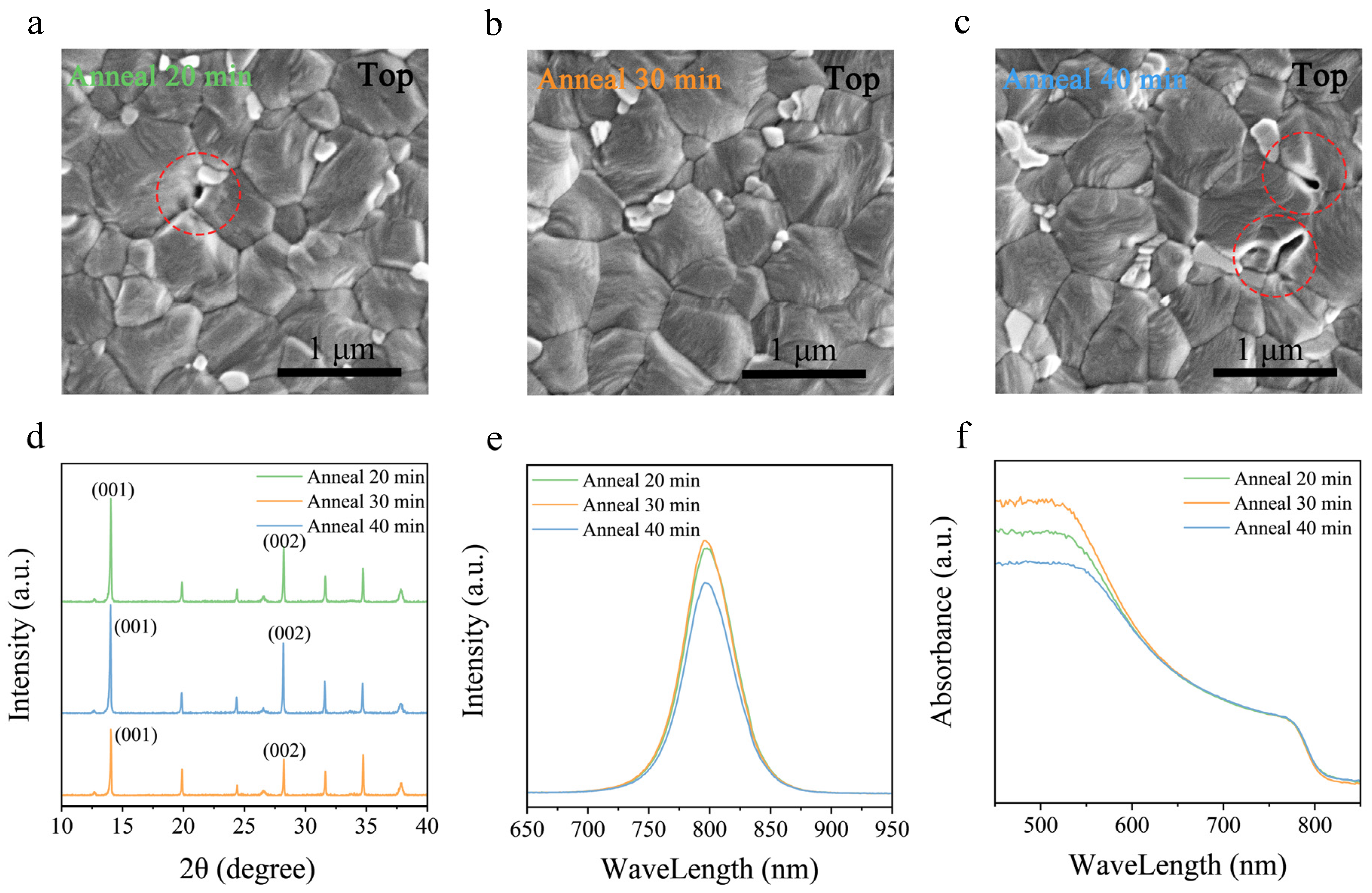
To further optimize the active layer process, we fixed the antisolvent dripping time at 19 s and then further studied the effect of annealing at 100 °C for different durations (20, 30, and 40 min) on perovskite films. Following a similar analysis procedure, we first examined the morphological changes of perovskite layers (Figure 3a–c). As a result, annealing at 100 °C for 20 min led to incomplete crystallization, as evidenced by the perovskite film exhibiting a relatively small grain size, together with visible grain boundaries. When the annealing time was increased to 30 min, a more compact and smoother perovskite surface with a larger grain size among the three samples was observed, which is beneficial for improving the efficiency and stability of perovskite devices; ref. [21] further confirms that 20 min is insufficient for complete crystallization. However, when the annealing time was further prolonged to 40 min, the perovskite films exhibited visible cracks and more of the PbI2 phase, indicating that excessive annealing induces film deterioration and defect formation. Accordingly, 30 min thermal annealing is preliminarily deemed suitable to facilitate grain growth.
Figure 3.
(a–c) SEM images, XRD patterns (d), PL spectra, (e) and UV-vis spectra (f) of perovskite films prepared at different annealing times of 20, 30, and 40 min.
Furthermore, the XRD patterns showed the weakest (001) and (002) peaks for the samples annealed for 20 min, while stronger (001) and (002) peaks were observed as the annealing time increased, indicating improved crystallinity of the perovskite films (Figure 3d) [22]. However, the sharpest (001) and (002) peaks were detected for the 30 min annealing time. In contrast, the 40 min annealing resulted in reduced peak intensity, accompanied by the appearance of a PbI2 diffraction peak at approximately 12.6°. The integrated intensity ratio of I (PbI2)/I (001) increased from 6.18% at 30 min to 12.02% at 40 min (Figure S3, Supplementary Materials), indicating that excessive annealing promotes PbI2 segregation and film degradation. We also performed PL and UV-vis measurements to verify the improved film quality of the film annealed for 30 min. As a result, the films treated with 30 min annealing exhibited the strongest PL intensity and light absorbance intensity, as predicted. In summary, the XRD patterns revealed a process of continuous grain growth followed by film deterioration. The PL and UV-vis spectra further confirmed the improved film quality for the 30 min annealing time (Figure 3e,f). All these results are consistent with the SEM observations and collectively confirmed the optimal annealing time is 30 min.
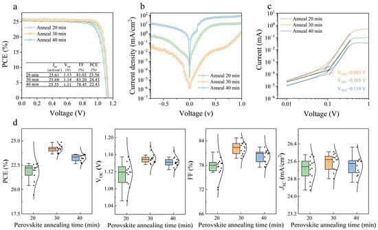
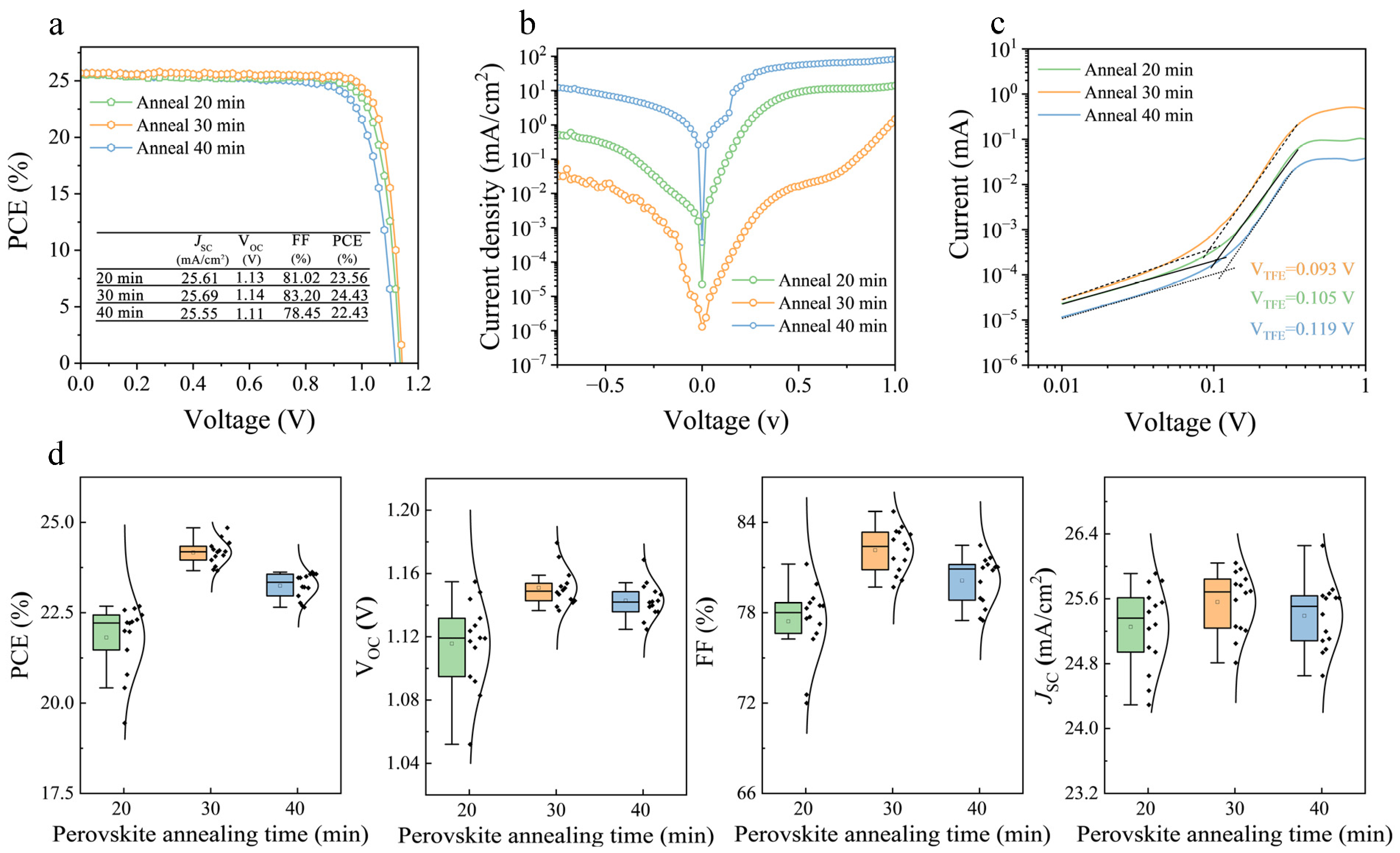
Finally, to gain a deeper understanding of the effect of different annealing times on device performance, inverted PSCs with structure of FTO/Me-4PACz/PVK/PCBM/BCB/Ag were fabricated. As illustrated in Figure 4a, the champion device treated with 20 min achieved a PCE of 23.56%, with a short-circuit density (Jsc) of 25.61 mA/cm2, a fill factor (FF) of 81.02% and an open-circuit voltage (Voc) of 1.13 V. In comparison, the champion device annealed for 30 min delivered the best PCE of 24.43%, with a Jsc of 25.69 mA/cm2, an FF of 83.20%, and a Voc of 1.14 V. When the annealing time was further prolonged to 40 min, the champion device exhibited a PCE of 22.43%, with a Jsc of 25.55 mA/cm2, an FF of 78.45%, and a Voc of 1.11 V. This result can be attributed to different perovskite film qualities resulting in different levels of non-radiative recombination and defect states [23,24]. Accordingly, the dark J-V characteristic shown in Figure 4b revealed that the device annealed for 30 min exhibited the lowest dark current, indicating effectively suppressed carrier leakage and trap-assisted recombination. In addition, the space charge limited current (SCLC) measurements, based on the electron-only structure of FTO/SAM/PVK/Spiro-OMeTAD/Ag, were performed to quantify the amount of defect density of perovskite films under different annealing conditions. In Figure 4c, the trap-filled limit voltage (VTFL) was 0.105 V, 0.093 V, and 0.119 V, corresponding to annealing for 20, 30, and 40 min, respectively. Defect density (Ntrap) can be further calculated from the VTFL value by the following equation:
where L is the thickness of perovskite film (600 nm), q is the elementary charge, and ɛ and ε0 are the relative permittivity of the perovskite and the vacuum permittivity (8.854 × 10⁻¹² F m−1), respectively [25,26]. Accordingly, the films prepared at a 30 min annealing time presented the lower Ntrap of 9.14 × 10⁻¹⁴ cm−3, compared with the films prepared at 20 min (Ntrap = 1.03 × 10⁻¹⁵ cm−3) and 40 min (Ntrap = 1.17 × 10⁻¹⁵ cm−3). To further verify the reproducibility of device performance, the PV parameters of independent devices fabricated in the same batch under different conditions were statistically collected for comparison (Figure 4d). Each data point represents a single device, and 14 devices were tested under each condition. The statistical distributions, mean values, and standard deviations for each parameter are summarized in Table S1 in the Supplementary Materials. Obviously, devices with annealing treatment for 30 min presented a more concentrated distribution and overall enhanced PV parameters, especially in FF and Voc, indicating better device performance and reproducibility. Therefore, we basically determined the optimal 19 s antisolvent dripping time and 30 min annealing time for perovskite film formation.
Figure 4.
(a) J-V curves, (b) dark J-V curves, (c) SCLC characteristics, and (d) PV parameters distribution for different annealing times.
4. Conclusions
In summary, we systematically investigated the influence of antisolvent dripping time and annealing time on the quality of a perovskite active layer and the performance of PSCs. By meticulously studying the crystallization morphology, optical properties, and defect characteristics of perovskite films under different process conditions, we found that the antisolvent dripping time directly affects the film integrity, whereas the annealing time mainly affects the grain growth. Finally, the optimal antisolvent dripping time of 19 s and annealing time of 30 min were determined. Under the optimized parameters, the champion device delivered an improved PCE of 24.43%, with a Jsc of 25.69 mA/cm2, an FF of 83.20% and a Voc of 1.14 V. These results reveal that precise control over the antisolvent dripping and annealing time is vital for lab-scale devices, with promising prospects for the repeatable manufacturing of large-area perovskite solar cells.
Supplementary Materials
The following supporting information can be downloaded at: https://www.mdpi.com/article/10.3390/coatings16070807/s1, Figure S1: PL spectra of perovskite films prepared at different annealing times of 20, 25, and 30 min. Figure S2: XRD (001) diffraction patterns of perovskite films prepared at antisolvent dripping times of 17, 19, and 21 s. Figure S3: XRD spectra of perovskite films prepared at different annealing times of 20, 30, and 40 min. Table S1: Statistical summary of photovoltaic parameters of 14 independent PSCs with different annealing times.
Author Contributions
Conceptualization and writing—original draft preparation, W.L. and F.X.; formal analysis, H.Z.; investigation and resources data curation, Q.C. and L.Z.; supervision and writing—review and editing, X.Z. and Y.L.; project administration and funding acquisition, Y.L. All authors have read and agreed to the published version of the manuscript.
Funding
This research is supported by the National Natural Science Foundation of China (W2521086, 52372139), Guangdong Basic and Applied Basic Research Foundation (2025A1515010515), Guangdong University of Technology SPOE Seed Foundation (SF2024111507), and 2025 Shanwei Talent Revitalization Plan for New Generation Electronic Information Industry (250421168940208).
Data Availability Statement
Data can be available on request.
Acknowledgments
We would like to thank the Analysis and Test Center of Guangdong University of Technology for the surface analysis of our samples.
Conflicts of Interest
There is no conflicts of interest to disclose.
References
- Liu, C.; Yang, Y.; Chen, H.; Xu, J.; Liu, A.; Bati, A.; Zhu, H.; Grater, L.; Hadke, S.; Huang, C.; et al. Bimolecularly passivated interface enables efficient and stable inverted perovskite solar cells. Science 2023, 382, 810–815. [Google Scholar] [CrossRef] [Scilit] [PubMed]
- Pu, X.; Cao, Q.; He, X.; Su, J.; Wang, W.; Zhang, X.; Wang, D.; Zhang, Y.; Yang, J.; Wang, T.; et al. Synergistic Crystallization Kinetics Modulation and Deep/Shallow Level Defect Passivation via an Organometallic Cobaltocenium Salt Toward High-Performance Inverted Perovskite Solar Cells. Adv. Energy Mater. 2024, 14, 2303972. [Google Scholar]
- Dong, Y.; Zhu, W.-X.; Wu, D.-T.; Li, X.; Westbrook, R.J.E.; Huang, C.-J.; Min, Z.; Hong, W.; Wang, B.; Min, G.; et al. Crystal Growth Modulation of Tin–Lead Halide Perovskites via Chaotropic Agent. J. Am. Chem. Soc. 2025, 147, 31578–31590. [Google Scholar] [CrossRef] [Scilit] [PubMed]
- Zhang, X.; Wu, S.; Zhang, H.; Jen, A.K.Y.; Zhan, Y.; Chu, J. Advances in inverted perovskite solar cells. Nat. Photonics 2024, 18, 1243–1253. [Google Scholar] [CrossRef] [Scilit]
- Taylor, A.D.; Sun, Q.; Goetz, K.P.; An, Q.; Schramm, T.; Hofstetter, Y.; Litterst, M.; Paulus, F.; Vaynzof, Y. A general approach to high-efficiency perovskite solar cells by any antisolvent. Nat. Commun. 2021, 12, 1878. [Google Scholar] [CrossRef] [Scilit] [PubMed]
- Jiang, X.; Liu, B.; Wu, X.; Zhang, S.; Zhang, D.; Wang, X.; Gao, S.; Huang, Z.; Wang, H.; Li, B.; et al. Top-Down Induced Crystallization Orientation toward Highly Efficient p-i-n Perovskite Solar Cells. Adv. Mater. 2024, 36, 2313524. [Google Scholar]
- Wang, K.; Tang, M.; Dang, H.X.; Munir, R.; Barrit, D.; Bastiani, M.D.; Aydin, E.; Smilgies, D.-M.; Wolf, S.D.; Amassian, A. Kinetic Stabilization of the Sol–Gel State in Perovskites Enables Facile Processing of High-Efficiency Solar Cells. Adv. Mater. 2019, 31, 1808357. [Google Scholar]
- Pallotta, R.; Degani, M.; Toniolo, F. On the synergistic interplay between annealing temperature and time and additive concentration for efficient and stable FAPbI3 perovskite solar cells. Mater. Today Adv. 2024, 24, 100541. [Google Scholar] [CrossRef] [Scilit]
- Chang, Y.-T.; Tien, C.-H.; Lee, K.-Y.; Tung, Y.-S.; Chen, L.-C. Evaporated MAPbI3 Perovskite Planar Solar Cells with Different Annealing Temperature. Energies 2021, 14, 2145. [Google Scholar] [CrossRef] [Scilit]
- Zhang, Y.; Kong, T.; Liu, Y. The Effect of Self-Assembled Bridging Layer on the Performance of Pure FAPbI3-Based Perovskite Solar Cells. Adv. Funct. Mater. 2024, 34, 2401391. [Google Scholar]
- Khan, J.I.; Yang, Y.; Palmer, J.R. Evaluation of interfacial photophysical processes by time-resolved optical spectroscopy in perovskite solar cells. Matter 2024, 7, 2536–2550. [Google Scholar] [CrossRef] [Scilit]
- Mao, J.; Iocozzia, J.; Huang, J.; Meng, K.; Lai, Y.; Lin, Z. Unraveling the Interfacial Homogeneity and Bulk Crystallization for Efficient and Stable Perovskite Solar Cells via Ionic Liquids. Energy Environ. Sci. 2018, 11, 772–799. [Google Scholar]
- Chen, J.; Liu, J.; Li, Y. Ultrasonic-Assisted Processing Combined with Gas Quenching for Fabricating High-Performance and Stable Inverted Perovskite Solar Cells. Adv. Funct. Mater. 2024, 34, 2314652. [Google Scholar]
- Wen, H.; Zhang, Z.; Guo, Y. Synergistic Full-Scale Defect Passivation Enables High-Efficiency and Stable Perovskite Solar Cells. Adv. Energy Mater. 2023, 13, 2301813. [Google Scholar]
- Huang, X.; Wu, B.; Zheng, N. Optimizing Solvent Chemistry for High-Quality Halide Perovskite Films. Acc. Mater. Res. 2025, 6, 40–51. [Google Scholar]
- Jeon, N.J.; Noh, J.H.; Kim, Y.C.; Yang, W.S.; Ryu, S.; Seok, S.I. Solvent engineering for high-performance inorganic–organic hybrid perovskite solar cells. Nat. Mater. 2014, 13, 897–903. [Google Scholar] [PubMed]
- Yang, X.; Ma, T.; Hu, H. Understanding and manipulating the crystallization of Sn–Pb perovskites for efficient all-perovskite tandem solar cells. Nat. Photonics 2025, 19, 426–433. [Google Scholar]
- Zhang, Y.; Liu, Y.; Zhao, Z. Reduction of Nonradiative Recombination at Perovskite/C60 Interface in Inverted Perovskite Solar Cells. Adv. Mater. 2025, 37, 2500501. [Google Scholar] [CrossRef] [Scilit]
- Tan, W.L.; McNeill, C.R. X-ray diffraction of photovoltaic perovskites: Principles and applications. Appl. Phys. Rev. 2022, 9, 021310. [Google Scholar] [CrossRef] [Scilit]
- Song, Y.; Zhang, X.; Wang, Y. Reinforcing Coverage of Self-assembled Monomolecular Layers for Inverted Perovskite Solar Cells with Efficiency of 25.70%. Angew. Chem. Int. Ed. 2024, 137, e202423827. [Google Scholar]
- Cao, Y.; Yang, L.; Yan, N. Buried interface modification for high performance and stable perovskite solar cells. Energy Environ. Sci. 2025, 18, 3659–3667. [Google Scholar] [CrossRef] [Scilit]
- Jia, X.; Zhang, K.; Gao, X. Defect passivation and crystallization modulation in methylammonium-free wide-bandgap perovskites for all-perovskite tandem solar cells. Sci. Adv. 2025, 11, eadv4501. [Google Scholar] [PubMed]
- Wang, S.; Sun, X.; Shi, J. Additive-Driven Enhancement of Crystallization: Strategies and Prospects for Boosting Photoluminescence Quantum Yields in Halide Perovskite Films for Light-Emitting Diodes. Adv. Mater. 2024, 36, 2413673. [Google Scholar]
- Yao, Y.; Wang, Q.; Chen, X. 25.91%-Efficiency and Durable Inverted Perovskite Solar Cells Enabled by a Multifunctional Molecule Mediated Precursor Engineering. Small 2024, 21, 2409568. [Google Scholar]
- Li, B.; Xing, J.; Budnik, V. Micromolecule Postdeposition Process for Highly Efficient Inverted Perovskite Solar Cells. ACS Appl. Mater. Interfaces 2025, 17, 14269–14277. [Google Scholar] [CrossRef] [Scilit] [PubMed]
- Cheng, H.; Liu, C.; Zhuang, J. KBF4 Additive for Alleviating Microstrain, Improving Crystallinity, and Passivating Defects in Inverted Perovskite Solar Cells. Adv. Funct. Mater. 2022, 32, 2204880. [Google Scholar] [CrossRef] [Scilit]
Disclaimer/Publisher’s Note: The statements, opinions and data contained in all publications are solely those of the individual author(s) and contributor(s) and not of MDPI and/or the editor(s). MDPI and/or the editor(s) disclaim responsibility for any injury to people or property resulting from any ideas, methods, instructions or products referred to in the content. |
© 2026 by the authors. Licensee MDPI, Basel, Switzerland. This article is an open access article distributed under the terms and conditions of the Creative Commons Attribution (CC BY) license.