


Abstract
To enable high-density multimode photonic integration, we propose and numerically demonstrate a plasmonic hybrid mode division multiplexer–demultiplexer with a sodium coating on a silicon-on-insulator (SOI) platform. The device enables simultaneous mode division multiplexing (MDM) and demultiplexing of the transverse magnetic modes TM0 and TM1 at λ = 1550 nm. Full-wave three-dimensional finite-difference time-domain (3D-FDTD) simulations confirm an insertion loss of 1.2 dB, an inter-modal crosstalk of −20.3 dB, and a compact footprint of 5 μm × 16 μm. Compared with representative SOI-based mode-selective couplers with longer conversion regions, the proposed design substantially reduces the coupling length and device footprint. This numerical study provides a potential route toward compact, high-density multimode photonic integration based on sodium-assisted hybrid plasmonics.
1. Introduction
The rapid convergence of microelectronics and photonics has intensified the demand for high-bandwidth, energy-efficient optical interconnects and on-chip signal processing. Photonic integrated circuits (PICs) are accordingly advancing toward higher integration density, smaller footprints, and heterogeneous/hybrid integration schemes—driven by the need to scale bandwidth, minimize power consumption, and enable system-in-package architectures in next-generation optical communication systems. Waveguide miniaturization is a cornerstone strategy for enhancing component density in PICs [1,2,3]. Surface plasmon polaritons (SPPs), supported at metal–dielectric interfaces, offer a compelling route to break the diffraction limit: they confine light to deep-subwavelength scales (<λ/10), enabling ultra-compact waveguides and functional devices [4,5,6,7,8].
Among conventional plasmonic metals, Ag and Au have been widely used because of their relatively low optical losses and mature nanofabrication processes. Ag generally provides the lowest loss among noble metals in the visible and near-infrared regions, whereas Au offers better chemical stability but suffers from interband absorption in the visible range. Cu is less expensive and more abundant, but its higher optical loss and oxidation tendency limit its plasmonic performance. Despite their broad use, these conventional metals still face a trade-off between optical loss, chemical stability, cost, and fabrication complexity. This motivates the exploration of alternative low-loss plasmonic materials for near-infrared photonic devices.
Alkali metals (such as sodium) exhibit exceptional performance, particularly in the near-infrared (NIR) region (800–2000 nm). Theoretically, sodium’s free electron relaxation time is longer than that of silver (approximately twice as long), thereby enhancing the material quality factor and reducing propagation losses in plasmonic waveguides; estimates indicate that its loss at 1550 nm is about 50% lower than that of silver-based materials. Beyond its outstanding optical properties, sodium offers significant cost advantages over precious metals, costing less than 1% of the market price of silver. These findings underscore sodium’s potential for low-loss plasmonic applications [9,10]. Sodium is chemically reactive and should not be exposed to ambient oxygen or moisture. For practical implementation, the Na layer should be introduced after completion of the standard SOI waveguide fabrication process, with deposition performed in an inert atmosphere. The Na layer in the proposed device is therefore regarded as an encapsulated functional plasmonic coating rather than an exposed metal surface. Possible encapsulation strategies include epoxy sealing, quartz cover protection, and dielectric passivation layers such as SiO2 or Al2O3. Accordingly, the proposed integration route should be considered as a low-temperature post-processing step after standard SOI waveguide fabrication. Encapsulation strategies for sodium films have also been experimentally demonstrated in previous studies. A research team performed both the spin-coating preparation and device assembly of sodium films within a glovebox under an inert atmosphere [11]. Upon completion, the sodium film was sealed between a quartz substrate and epoxy resin. This physical sealing can effectively reduce direct contact between the sodium film and ambient oxygen or moisture, thereby enabling stable optical performance after removal from the glovebox. In the work reported in Ref. [11], the sodium film was physically isolated from oxygen and moisture by quartz/epoxy packaging, and packaged sodium-based devices were reported to maintain stable optical performance over several months. Dielectric passivation layers such as SiO2 or Al2O3 may also be considered, but their barrier quality, continuity, and interface compatibility require further experimental verification. Sodium has a melting point of approximately 98 °C, whereas the device operates within a temperature range of 0–70 °C, which is below its melting point.
Mode division multiplexing (MDM) leverages orthogonal spatial modes to multiply channel capacity within a single waveguide, thereby enhancing spectral efficiency without requiring additional wavelengths or fibers [12,13,14,15]. While free-space MDM solutions offer wavelength-agnostic operation, their bulky optics and poor integrability limit on-chip deployment. In contrast, monolithic waveguide-based MDM is now the dominant paradigm, with asymmetric directional couplers (ADCs) being the most widely adopted architecture due to their compact footprint, design flexibility, and straightforward integration with silicon photonics platforms. ADCs rely on phase-matching between the fundamental mode of a narrow waveguide and a higher-order mode of a wider waveguide; when their effective indices align, efficient mode conversion occurs. Silicon-on-insulator (SOI) nanowire waveguides are the leading platform for on-chip MDM, benefiting from silicon photonics design process compatibility and mature fabrication infrastructure [16,17]. However, current state-of-the-art silicon-based MDM devices are constrained by a compromise between performance and scalability. For instance, Tan et al. developed a silicon-based hybrid demultiplexer that necessitates a 100 μm long mode conversion region [18]. While Zhuang et al. managed to reduce the loss, their design still demands a 34 μm coupling length [19]. Similarly, Jiang et al. proposed devices with low insertion loss and low crosstalk, but their coupling lengths remain 7 μm [20] and 7.5 μm [21], respectively. Furthermore, Ni et al. presented a silver-based ADC with a footprint of 17.1 μm × 1.33 μm and a 4.1 μm coupling length; nevertheless, its multi-step metallization process may increase fabrication complexity [22]. Collectively, these studies indicate that reducing the coupling length while maintaining acceptable insertion loss and crosstalk remains an important challenge for high-density on-chip MDM devices.
Here, we propose a sodium-based plasmonic hybrid mode division multiplexer–demultiplexer for SOI nanowires. By integrating a sodium metal layer to enhance evanescent field overlap, our ADC structure achieves TM0/TM1 multiplexing and demultiplexing in a footprint of 5 μm × 16 μm, with a coupling length of only 3.5 μm. Full-wave 3D-FDTD simulations confirm an insertion loss of 1.2 dB and an inter-modal crosstalk of −20.3 dB, demonstrating a viable pathway toward compact, high-density multimode photonic integration.
2. Theoretical Model and Analysis
In this work, all full-wave electromagnetic simulations were conducted using the 3D-FDTD method. To eliminate spurious reflections from the edges of the computational domain, perfectly matched layer (PML) absorbing boundary conditions were employed along all three spatial axes. The PML configuration consisted of 12 layers, with the parameters defined as kappa = 2, sigma = 0.25, and a polynomial order of 3, while the minimum and maximum layer counts were designated as 12 and 64, respectively. The convergence criterion was set to 1 × 10⁻⁵. Furthermore, the optical power recorded by every monitor was normalized to the input source power, ensuring a uniform evaluation of insertion loss and crosstalk across various input–output port pairings. Additionally, to precisely capture the highly confined hybrid plasmonic modes within the nanoscale gap, a finer override mesh was implemented specifically in the sodium-mediated hybrid coupling area, with a uniform grid resolution of dx = dy = dz = 20 nm.
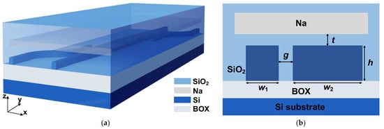
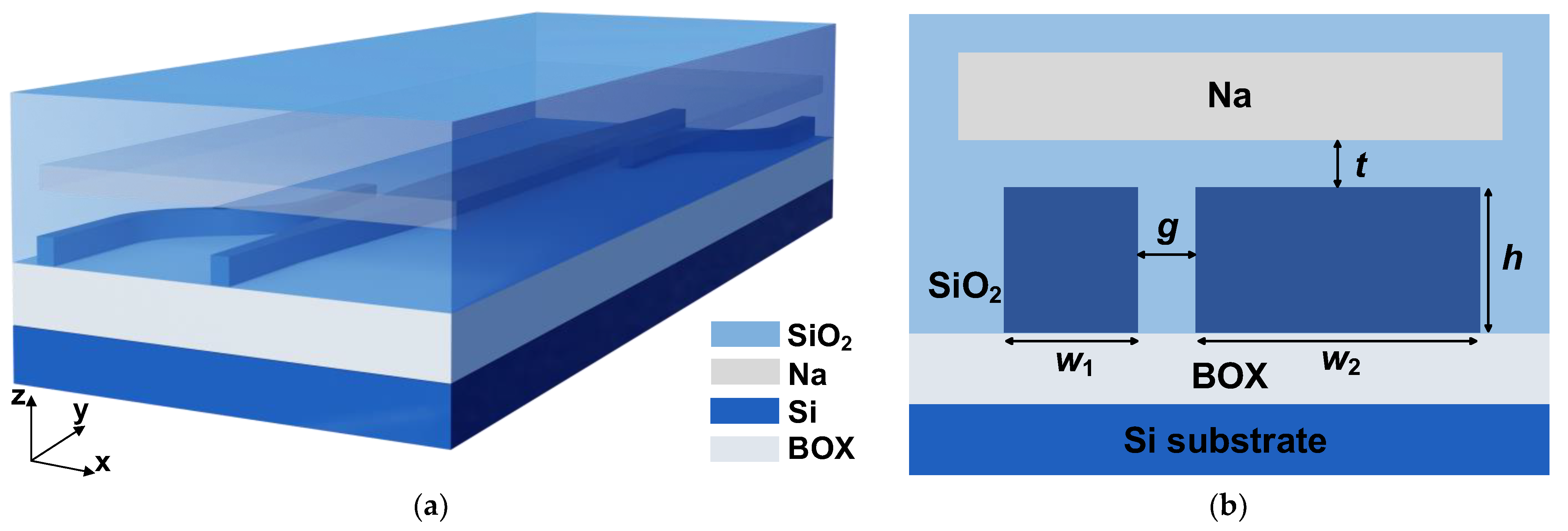
Figure 1 presents the three-dimensional architecture of our sodium-based hybrid mode division multiplexer/demultiplexer. The device is built on a silicon substrate and features a standard silicon-on-insulator (SOI) platform: a 2 μm thick SiO2 buried oxide (BOX) layer hosts two parallel silicon nanowire waveguides with a height of 220 nm (h = 220 nm)—one narrow (200 nm wide) supporting only the fundamental TM0 mode and one wider (675 nm wide) capable of guiding both TM0 and TM1 modes. A thick sodium layer is spin-coated over the coupling region, where it strongly enhances evanescent field overlap between the waveguides and tailors the dispersion to enable phase matching at 1550 nm. In the simulation model, a SiO2 spacer layer is used to define the optical coupling region and the vertical mode distribution; the parameter t denotes the vertical gap thickness between the Na film and the Si waveguides, which is controlled by this spacer layer. In practical devices, reliable environmental protection of the Na layer would require dense, continuous encapsulation, such as quartz/epoxy sealing or verified dielectric barrier layers. Simulations are performed at λ = 1550 nm, with the following complex refractive indices assigned: ñSilica = 1.444 for SiO2, ñSi = 3.476 for silicon (Si), and ñNa = 0.0447 + 6.9874i for the sodium (Na) film [11]. Material dispersion was included in all simulations.
Figure 1.
(a) Three-dimensional schematic of the sodium-based hybrid plasmonic mode division multiplexer–demultiplexer; (b) cross-sectional view of the mode coupling region.
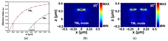
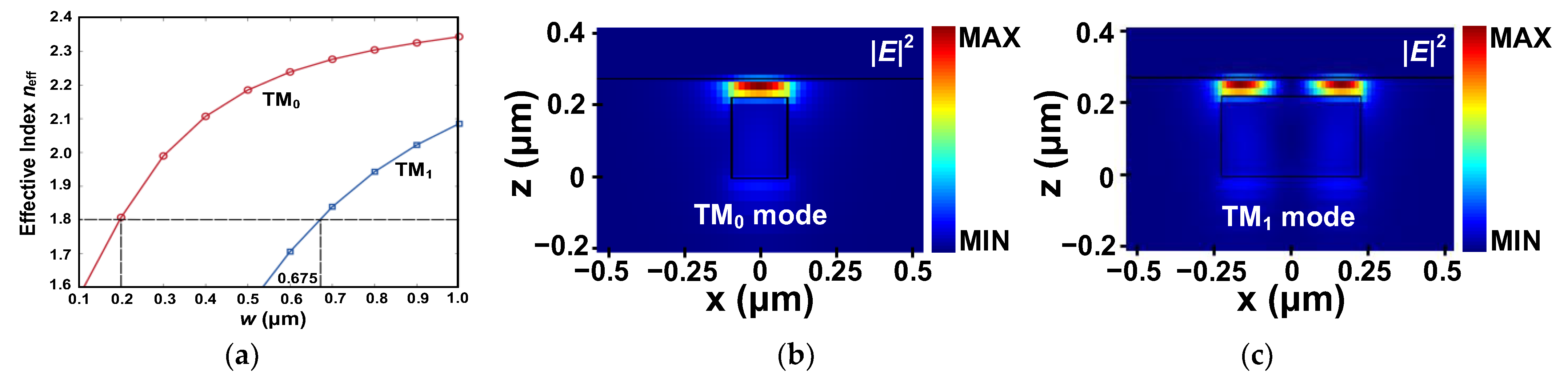
Mode solver simulations were conducted to analyze the guided TM modes in sodium-based hybrid plasmonic waveguides as a function of width (0.1–1.0 μm) at λ = 1550 nm, as shown in Figure 2a. As the waveguide width increases, the supported mode spectrum evolves from a single fundamental mode (TM0 only) to multiple higher-order modes—enabling multimode operation above ~520 nm in width. The effective indices (neff) of the TM0 mode in a 200 nm-wide waveguide and the TM1 mode in a 675 nm-wide waveguide intersect at neff ≈ 1.8, satisfying the phase-matching condition required for efficient mode conversion. This width pair—w1 = 200 nm and w2 = 675 nm—was therefore adopted in our asymmetric directional coupler design. Figure 2b,c present the corresponding normalized |E|2 field distributions of the TM0 and TM1 modes at these widths.
Figure 2.
(a) Effective index map of the sodium-based hybrid plasmonic waveguide at 1550 nm as a function of the nanowire waveguide width; (b) normalized |E|2 intensity distributions of the TM0 mode (at w1 = 200 nm); (c) normalized |E|2 intensity distributions of the TM1 mode (at w2 = 675 nm).
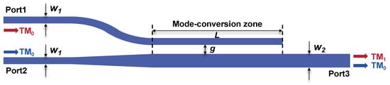
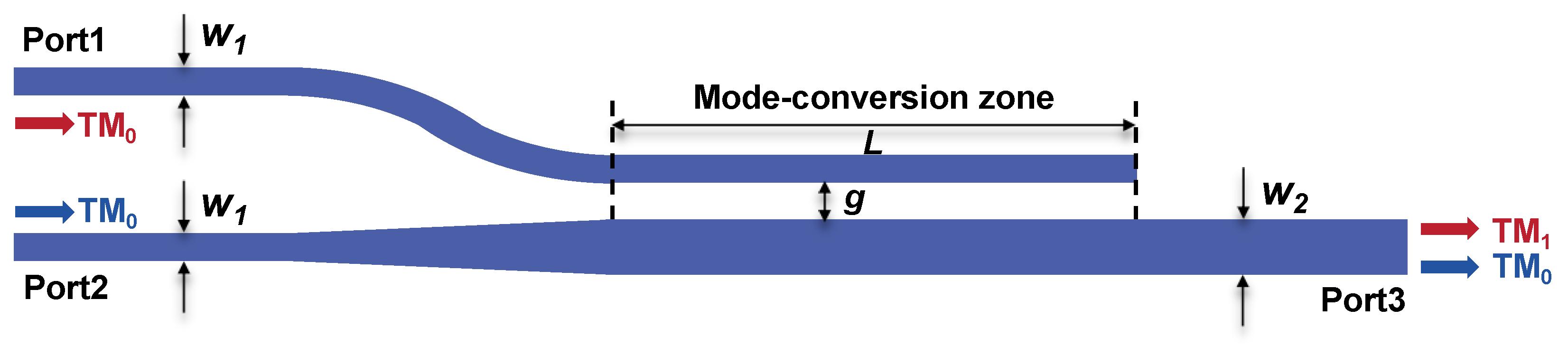
Figure 3 illustrates the structure of a sodium-based hybrid plasmonic mode division multiplexer/demultiplexer with the following specific parameters: the single-mode waveguide has a width of w1 = 200 nm; the multimode waveguide has a width of w2 = 675 nm; the spacing between the single-mode and multimode waveguides is g = 200 nm; the coupling length is L = 3.5 μm; the curved waveguide consists of two circular arcs.
Figure 3.
Structural diagram of a sodium-based hybrid plasmonic mode division multiplexer.
The mode division multiplexing process works as follows: When the 1550 nm TM0 mode is launched into Port 1, it couples from the single-mode waveguide to the multimode waveguide in the mode-conversion zone and converts to the TM1 mode. When a 1550 nm TM0 mode is input through Port 2, it continues to propagate as the TM0 mode in the multimode waveguide without coupling to the TM0 mode in the single-mode waveguide at the mode-conversion zone. Notably, although the TM0 mode input through Port 2 does not undergo a higher-order mode conversion, the lateral distribution of its mode field expands as the waveguide width increases. Ultimately, both TM0 and TM1 modes are output through Port 3, achieving dual-mode MDM. Mode demultiplexing is the inverse process.
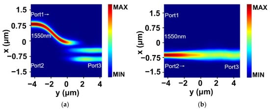
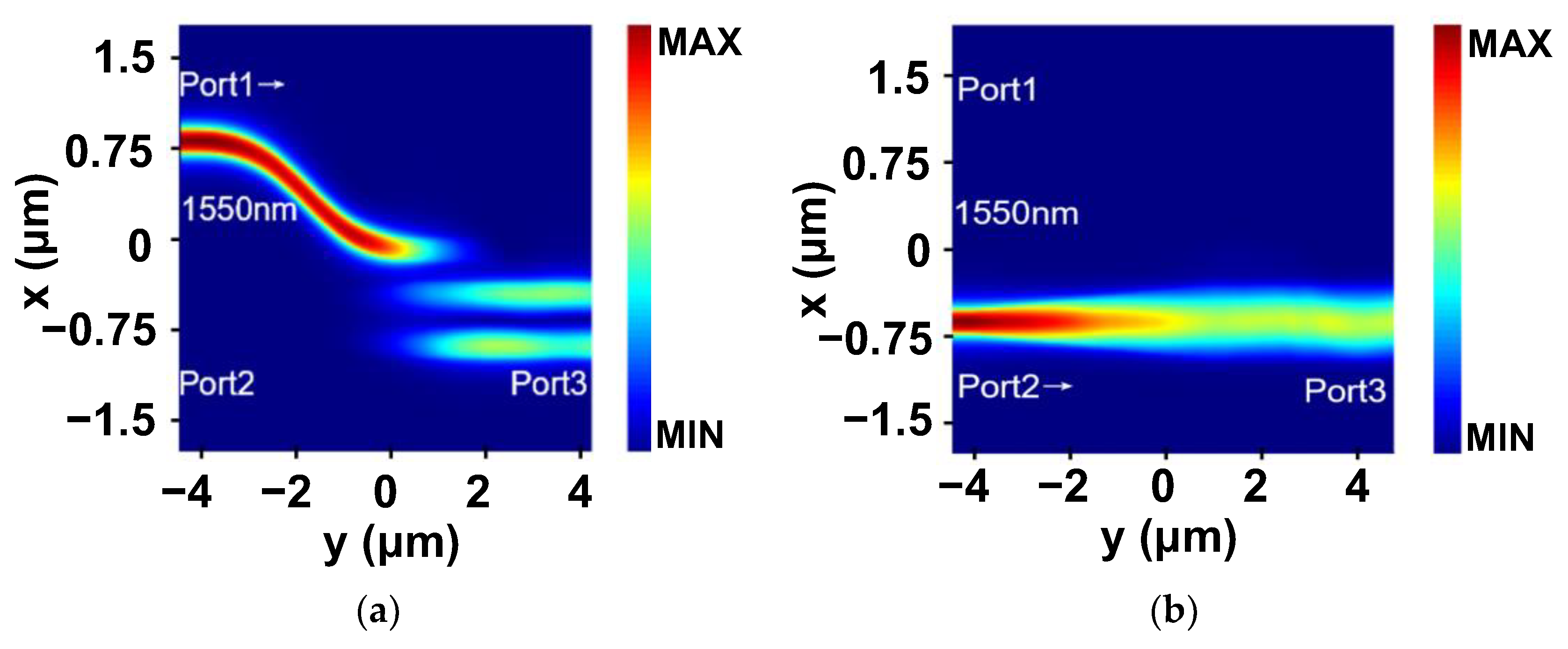
Figure 4 shows the steady-state field distribution of a sodium-based hybrid plasmonic mode division multiplexer/demultiplexer. Figure 4a depicts the field distribution when a 1550 nm TM0 beam is incident at Port 1, demonstrating that the majority of the incident energy couples into the multimode waveguide and converts to the TM1 mode. Figure 4b illustrates the field distribution when the same 1550 nm TM0 beam is incident at Port 2.
Figure 4.
Steady-state field distribution of the multiplexing process. (a) Light is input from Port 1; (b) light is input from Port 2.
Figure 5a,b show the transmission spectra of broadband TM-polarized light incident at Port 1 and Port 2, respectively. Figure 5a shows the transmission from Port 1 to Port 3, where the input TM0 mode couples into the multimode waveguide and converts to TM1. The transmission spectrum remains smooth across the investigated wavelength range, confirming stable mode conversion. Figure 5b shows the transmission spectrum for the Port 2 to Port 3 path, where the TM0 mode propagates in the multimode waveguide without coupling to the single-mode waveguide. The transmission efficiency at the central wavelength of 1550 nm reaches approximately 93%, with efficiency remaining above 85% across the 1200–1700 nm wavelength range, demonstrating an operational bandwidth of 500 nm.
Figure 5.
Transmission spectrum of the multiplexing process. (a) Light is input from Port 1; (b) light is input from Port 2.
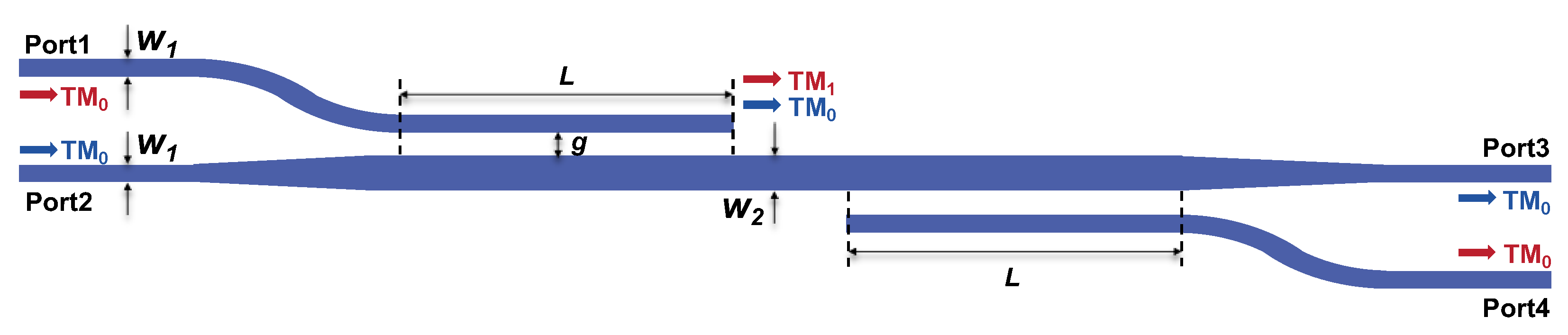
Figure 6 illustrates a hybrid plasmonic mode division multiplexing–demultiplexing structure. This design reverses the conventional mode division multiplexing architecture, maintaining identical parameters: a single-mode waveguide (w1 = 200 nm), a multimode waveguide (w2 = 675 nm), a 200 nm spacing between them, and a 3.5 μm coupling length. The ultrashort coupling length arises from the enhanced evanescent field overlap induced by the Na layer, resulting in a much higher coupling coefficient. The symmetric layout enables reciprocal multiplexing and demultiplexing functionality (Port 1/2 vs. Port 3/4). For instance, when light enters from Port 1, the TM0 mode transforms into TM1 mode in the first coupling zone and propagates through the multimode waveguide. It then reverts to TM0 mode in the second coupling zone before exiting through Port 4. Conversely, the TM0 mode incident from Port 2 maintains its original path through the main waveguide and exits as TM0 mode from Port 3.
Figure 6.
Structural diagram of a sodium-based hybrid plasmonic mode division multiplexer–demultiplexer.
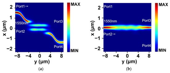
Figure 7 illustrates the steady-state field distribution of a sodium-based hybrid plasmonic mode multiplexer–demultiplexer. Figure 7a shows the steady-state field distribution when a 1550 nm TM0 mode is incident at Port 1. The TM0 beam first couples from a single-mode waveguide to a multimode waveguide in the mode coupling zone, converting into a TM1 mode. It then undergoes decoupling, transitioning from TM1 to TM0 mode, and is ultimately output at Port 4. Figure 7b depicts the steady-state field distribution when the same 1550 nm TM0 beam is incident at Port 2. The TM0 beam incident at Port 2 shows minimal coupling between the mode coupling and decoupling regions. Throughout the transmission process, the TM0 mode maintains its transmission state and is finally output at Port 3.
Figure 7.
Steady-state field distribution of the multiplexing and demultiplexing process. (a) Light is input from Port 1; (b) light is input from Port 2.
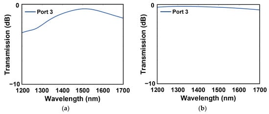
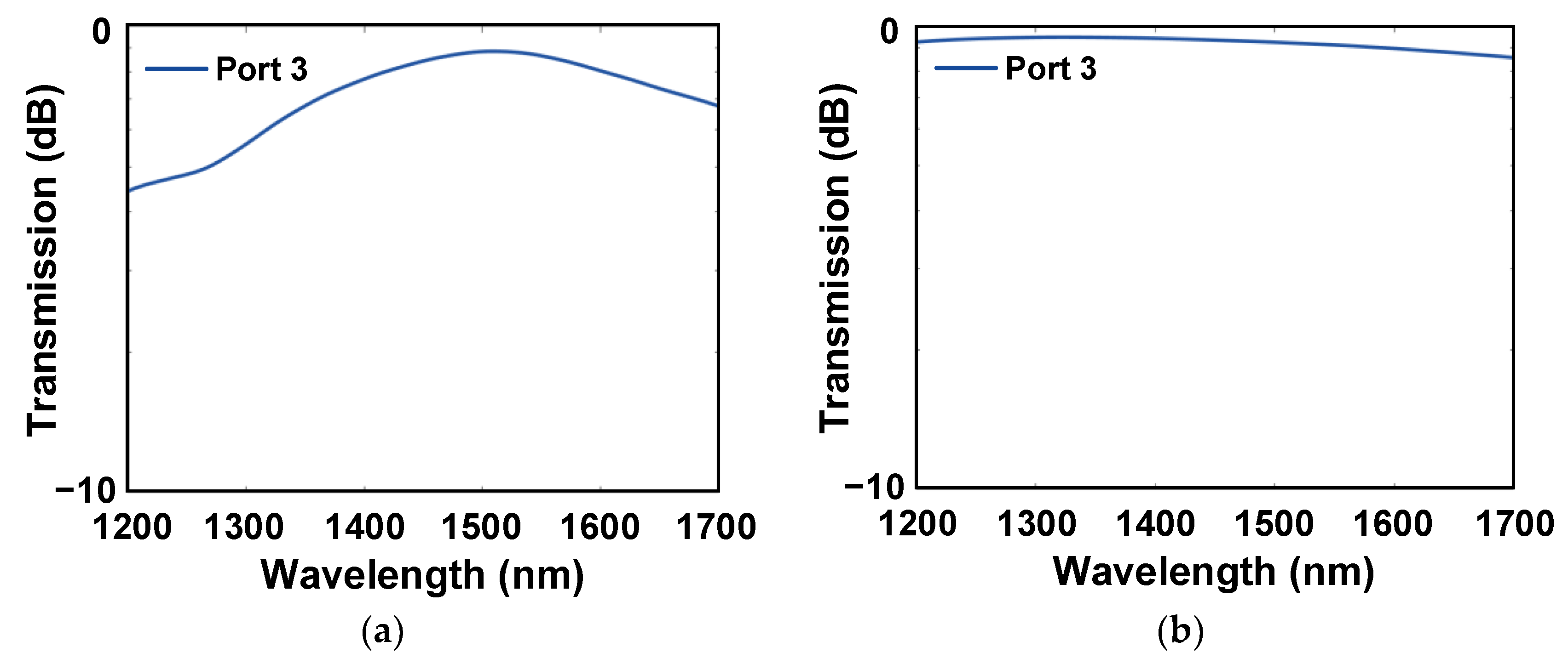
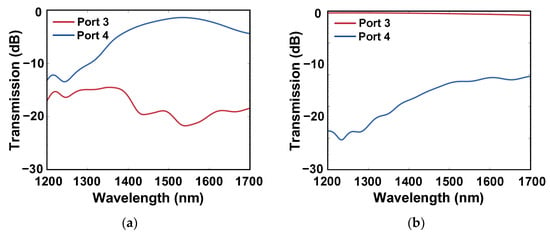
Figure 8 presents the transmission spectra of a sodium-based hybrid plasmonic mode division multiplexing–demultiplexing structure, with Table 1 and Table 2 summarizing the insertion loss and crosstalk for the target and undesired output channels. Figure 8a displays the transmission spectra measured at Port 3 and Port 4 when a broadband TM0 light source is placed at Port 1. At a central wavelength of 1550 nm, the transmission is 0.7% at Port 3 and 75% (corresponding to insertion loss IL = 1.2 dB) at Port 4, with a crosstalk of approximately −20.3 dB between the two channels. Figure 8b shows the transmission spectra measured at Port 3 and Port 4 when the broadband TM0 mode is incident at Port 2. At a central wavelength of 1550 nm, transmission is 84% (corresponding to insertion loss IL = 0.8 dB) at Port 3 and 0.6% at Port 4, with a crosstalk of −21.5 dB between the two channels. The insertion loss (IL) mentioned above is defined as follows:
where Ptarget is the output power at the desired port, and Pin is the input power launched into the device. The crosstalk (CT) is defined as follows:
where Pundesired is the power leaked to the unintended output port.
Figure 8.
Transmission spectrum of the multiplexing and demultiplexing process. (a) Light is input from Port 1; (b) light is input from Port 2.
Table 1.
Insertion loss for each input–output port combination.
Table 2.
Crosstalk for each input–output port combination.
As summarized in Table 3, the proposed sodium-based asymmetric directional coupler achieves a compact coupling length of 3.5 μm, which is shorter than those of previously reported Si-based devices [18,19,20] and the Au-assisted [21] or Ag-assisted hybrid plasmonic device [22]. However, we do not claim that the proposed device outperforms all previous devices in every metric. The insertion loss and crosstalk of the proposed device are not the lowest among all reported works, because the enhanced subwavelength modal confinement introduced by sodium-based hybrid plasmonic coupling also leads to additional ohmic loss. Therefore, the main advantage of this design lies in its compact footprint and short coupling length while maintaining acceptable simulated insertion loss and crosstalk. The proposed device should be regarded as a compact-footprint solution for high-density multimode photonic integration, with sodium integration implemented through low-temperature, encapsulated post-processing after standard SOI waveguide fabrication. Compared with noble-metal-assisted hybrid couplers, the proposed Na-assisted design represents an alternative post-processing route based on encapsulated sodium coatings. However, because elemental sodium requires inert-atmosphere handling and reliable encapsulation, its practical integration should be regarded as a low-temperature post-processing step rather than a fully standard front-end silicon fabrication process.
Table 3.
Performance comparison of silicon-based MDM devices.
3. Robustness Analysis
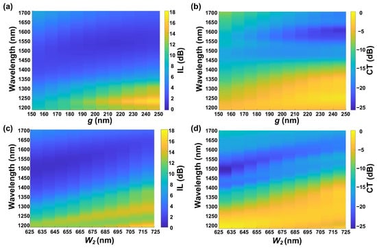
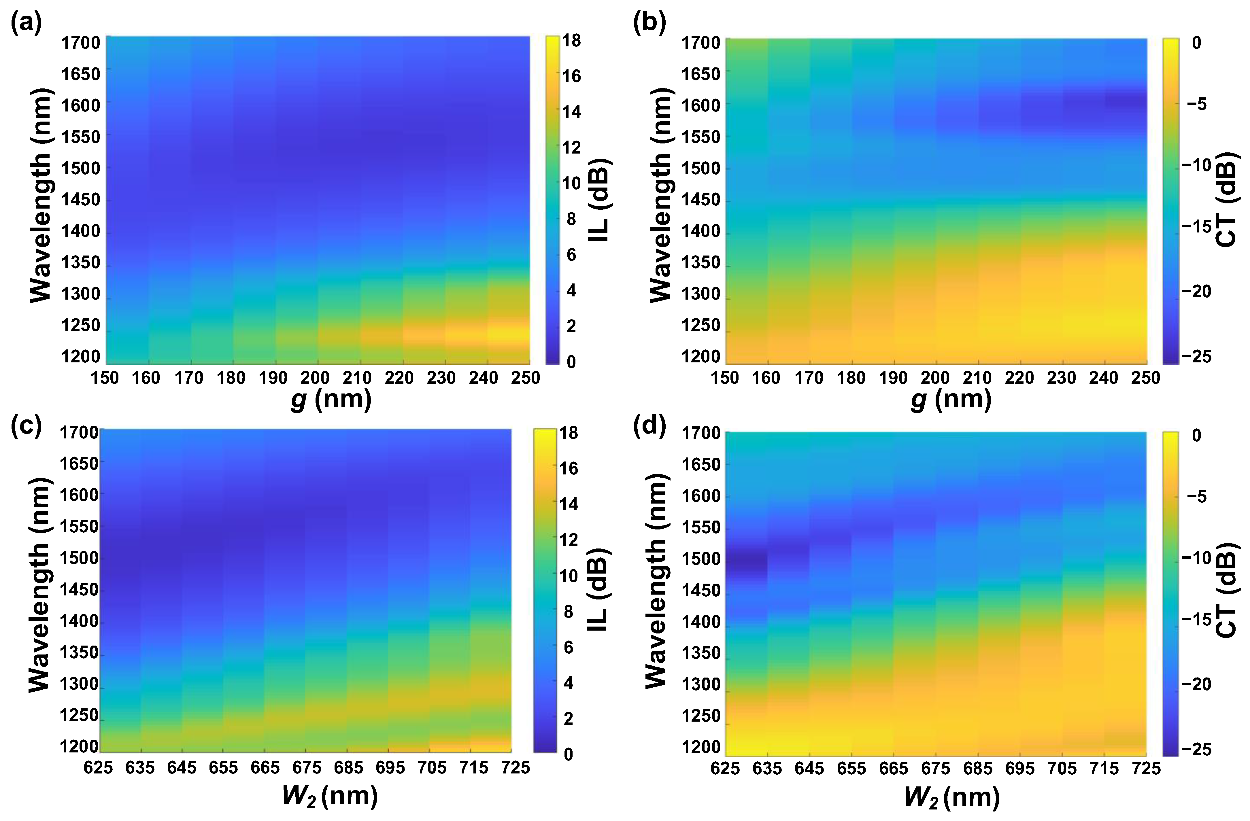
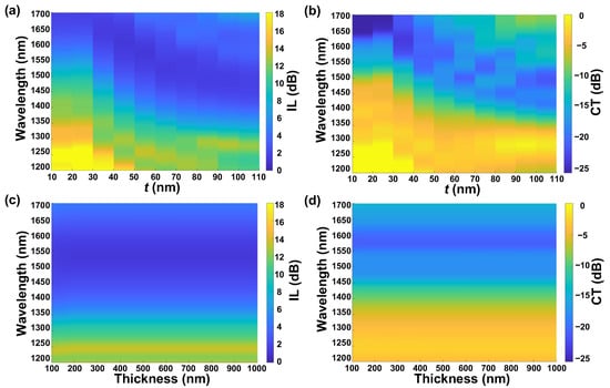
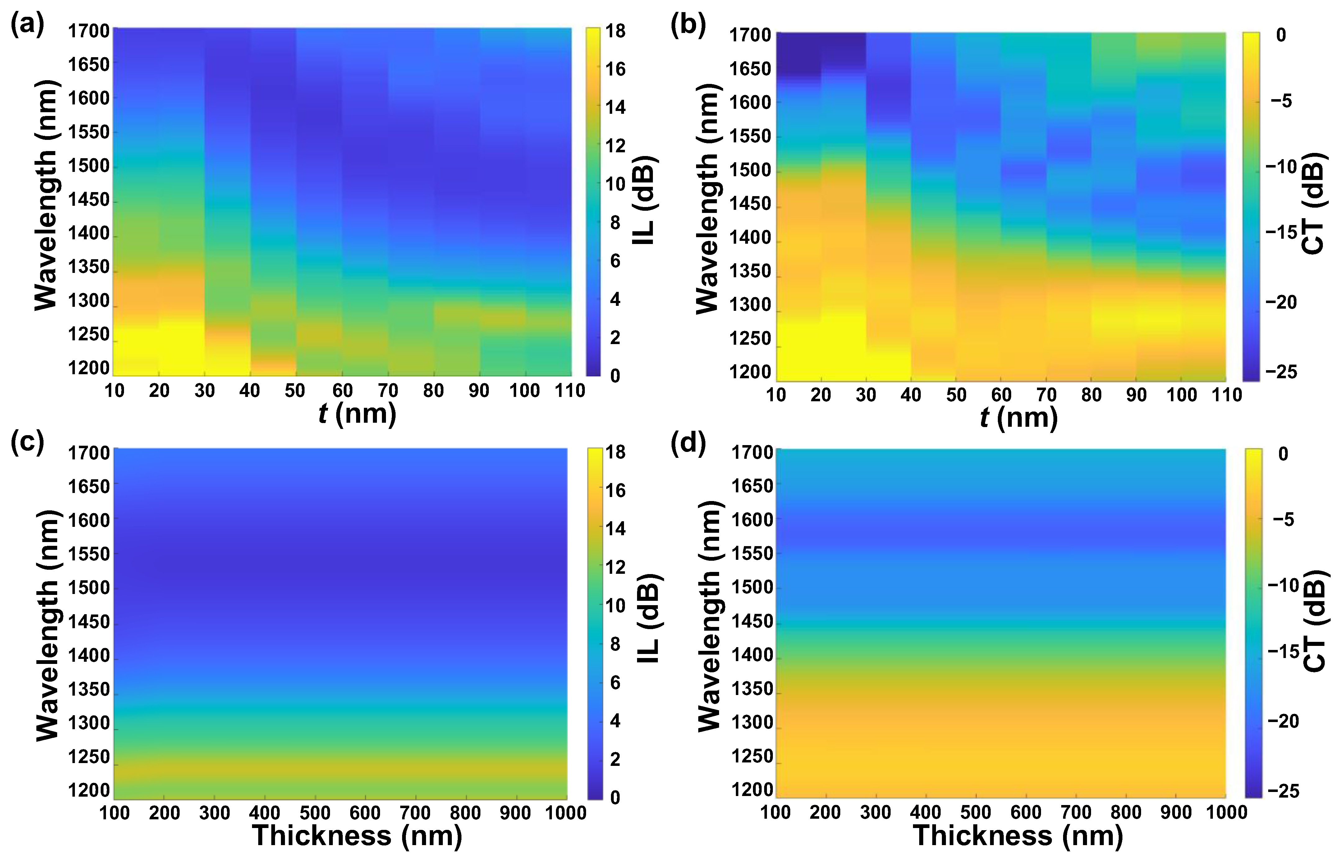
To evaluate the fabrication tolerance of the proposed device, robustness analyses were performed for both the waveguide geometry and sodium-related structural parameters. The corresponding parameter maps are provided as Figure 9 and Figure 10.
Figure 9.
Robustness maps for waveguide-geometry parameters. (a,b) IL and CT vs. g; (c,d) IL and CT vs. W2.
Figure 10.
Robustness maps for sodium-related structural parameters. (a,b) IL and CT vs. t; (c,d) IL and CT vs. Na-film thickness.
The tolerance maps reveal that the optical characteristics of the device change gradually in the vicinity of the 1550 nm target wavelength. This smooth variation suggests that neither the insertion loss nor the crosstalk relies on a narrow, sharp resonance; rather, they maintain acceptable fabrication margins. To evaluate these tolerances quantitatively, a performance penalty threshold was defined as either a 1 dB rise in IL or a 1 dB deterioration in the absolute value of CT.
Regarding the waveguide gap (g), the minimum IL is achieved at g = 200 nm. A deviation of g to around 180 nm and 220 nm causes the IL to rise by roughly 1 dB, yielding a tolerance of about ±20 nm. Similarly, the optimal CT is found near g = 200 nm, and a deviation of g to 190 nm and 210 nm results in a 1 dB CT penalty, which translates to a tolerance of ±10 nm. As for the multimode waveguide width (W2), the minimum IL is observed at W2 = 675 nm. Changing W2 to approximately 665 nm and 685 nm results in a ~1 dB IL increase, indicating a ±10 nm tolerance. Furthermore, the 1 dB deterioration limit for CT is reached when W2 is near 665 nm and 685 nm, corresponding to a tolerance of about ±10 nm. These results indicate that g and W2 are the most critical geometric dimensions, requiring priority in fabrication control.
Regarding the gap thickness t between the Na film and the Si waveguide, the lowest IL is observed at t ≈ 50 nm. Changing t to 40 nm and 60 nm leads to an IL increase of 1 dB, which indicates a tolerance of about ±10 nm. Meanwhile, the CT degrades by approximately 1 dB when t reaches approximately 40 nm or 60 nm, corresponding to a tolerance of about ±10 nm. In contrast, varying the sodium-film thickness across the 100–1000 nm range exerts a significantly weaker impact. Provided that the sodium layer is thick enough to sustain the desired hybrid plasmonic mode, any additional increase in its thickness barely affects the modal distribution or transmission performance.
4. Fabrication Feasibility
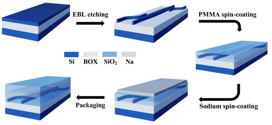
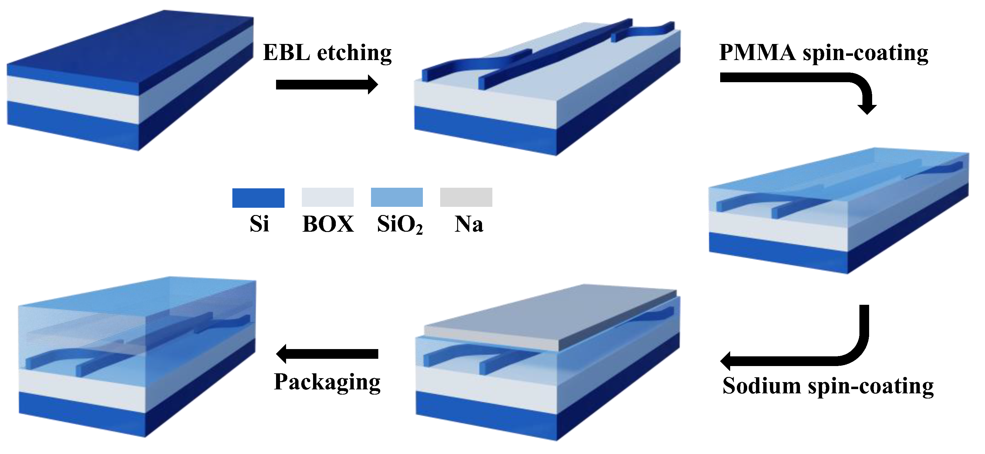
Although the present work focuses on numerical design, a feasible fabrication route can be proposed based on previously demonstrated encapsulated sodium processing, while future device-level experimental validation is still required. Figure 11 demonstrates the fabrication process flow of the proposed sodium-based hybrid plasmonic mode (de)multiplexer. The process starts from an SOI wafer with a 220 nm thick top silicon layer. The narrow silicon waveguide, multimode silicon waveguide, and coupling region are patterned by electron-beam lithography (EBL) and defined by dry etching. A dielectric spacer layer, such as SiO2, can then be deposited to adjust the optical mode distribution and the vertical spacing. Subsequently, sodium is introduced in the coupling region under an inert atmosphere. Following the thermo-assisted spin-coating technology reported by Wang et al. [11], molten sodium can be spin-coated to form a continuous Na film, as demonstrated in previous work. Finally, the Na layer should be immediately encapsulated using epoxy sealing and a quartz cover to prevent direct exposure to oxygen and moisture. This sodium-related process is therefore regarded as a low-temperature post-processing step after standard SOI waveguide fabrication. Prototype fabrication, Na film uniformity control, packaging reliability, and experimental verification of insertion loss and crosstalk will be the focus of future work.
Figure 11.
Fabrication process flow of the sodium-based hybrid plasmonic mode division multiplexer–demultiplexer.
5. Discussion: Limitations and Interface Stability
The present study is based on idealized numerical simulations using smooth interfaces. In practical devices, performance may be affected by Na-film quality, including surface roughness, thickness nonuniformity, native oxide formation, and possible interfacial layers between Na and the surrounding dielectric materials. Because the hybrid plasmonic mode is strongly confined near the Na–dielectric interface, surface roughness may increase scattering loss. Similarly, native oxide or interdiffusion layers may modify the effective optical constants. Therefore, although the robustness analysis indicates finite tolerance windows for the designed structural parameters, experimental realization will require careful control of Na-film uniformity, interface cleanliness, and encapsulation reliability. Future work should include AFM-based roughness characterization, XPS analysis of surface oxidation, cross-sectional TEM characterization of the interface, and direct measurement of insertion loss and crosstalk in fabricated prototypes.
6. Conclusions
This work numerically demonstrates a compact mode-division multiplexing and demultiplexing device based on a sodium-assisted hybrid plasmonic asymmetric directional coupler on an SOI platform. The structure comprises a 200 nm-wide single-mode waveguide and a 675 nm wide multimode waveguide, separated by a 200 nm gap and coupled over a length of 3.5 μm. With an overall footprint of just 5 μm × 16 μm, the device achieves an insertion loss of 1.2 dB and a crosstalk of −20.3 dB at 1550 nm. Compared with several representative Si-based MDM couplers, the proposed device offers a shorter coupling length, although its insertion loss and crosstalk are not the lowest among all reported devices. Moreover, the sodium coating may be integrated with silicon photonic platforms through low-temperature, encapsulated post-processing, suggesting a possible route toward compact multimode photonic circuits. Nevertheless, the present results are based on idealized numerical simulations. Future work will focus on prototype fabrication, sodium-film uniformity, interface characterization, packaging reliability, and experimental verification of insertion loss and crosstalk.
Author Contributions
Conceptualization, Y.Z.; methodology, Y.Z.; software, X.L.; validation, Y.Z., Z.S., and W.L.; formal analysis, Y.Z.; investigation, Y.Z.; resources, Y.Z.; data curation, X.L.; writing—original draft preparation, X.L.; writing—review and editing, H.Z.; visualization, X.L.; supervision, Y.Z.; project administration, Y.Z.; funding acquisition, Y.Z. and H.Z. All authors have read and agreed to the published version of the manuscript.
Funding
This research was funded by the National Natural Science Foundation of China, grant number 12404366, and the General Program of Fundamental Scientific Research (Natural Sciences) for Higher Education Institutions in Jiangsu Province, grant number 24KJB140006.
Institutional Review Board Statement
Not applicable.
Informed Consent Statement
Not applicable.
Data Availability Statement
All relevant data are included within this paper.
Conflicts of Interest
The authors declare no conflicts of interest.
Abbreviations
The following abbreviations are used in this manuscript:
| MDM | Mode division multiplexing; |
| SOI | Silicon-on-insulator; |
| TM | Transverse magnetic; |
| SPPs | Surface plasmon polaritons; |
| ADC | Asymmetric directional coupler; |
| PICs | Photonic integrated circuits; |
| CMOS | Complementary metal-oxide-semiconductor; |
| BOX | Buried oxide; |
| 3D-FDTD | Three-dimensional finite-difference time domain; |
| IL | Insertion loss; |
| CT | Crosstalk. |
References
- Siew, S.Y.; Li, B.; Gao, F.; Zheng, H.Y.; Zhang, W.; Guo, P.; Xie, S.W.; Song, A.; Dong, B.; Luo, L.W.; et al. Review of silicon photonics technology and platform development. J. Light. Technol. 2021, 39, 4374–4389. [Google Scholar] [CrossRef] [Scilit]
- Anwar, R.S.; Ning, H.; Mao, L. Recent advancements in surface plasmon polaritons-plasmonics in subwavelength structures in microwave and terahertz regimes. Digit. Commun. Netw. 2018, 4, 244–257. [Google Scholar] [CrossRef] [Scilit]
- Kim, J.T.; Park, S.; Ju, J.J.; Lee, S.; Kim, S. Low bending loss characteristics of hybrid plasmonic waveguide for flexible optical interconnect. Opt. Express 2010, 18, 24213–24220. [Google Scholar] [CrossRef] [Scilit] [PubMed]
- Ichiji, N.; Kikuchi, H.; Yessenov, M.; Schepler, K.L.; Abouraddy, A.F.; Kubo, A. Observation of space-time surface plasmon polaritons. Nat. Commun. 2025, 16, 10697. [Google Scholar] [CrossRef] [Scilit] [PubMed]
- Yang, L.; Li, P.; Wang, H.; Li, Z. Surface plasmon polariton waveguides with subwavelength confinement. Chin. Phys. B 2018, 27, 77–91. [Google Scholar] [CrossRef] [Scilit]
- Feng, Y.; Chao, K.; Wu, K.; Yuan, S.; Khosla, A.; Yang, R.; Rosei, F.; Zhang, H. Plasmonic photoelectric detection engineering: Basic principle, design strategies and challenges. Rep. Prog. Phys. 2025, 88, 096401. [Google Scholar] [CrossRef] [Scilit]
- Mohammad, S.; Pourziad, A.; Bigbaghlou, R.G. Hybrid MIM plasmonic waveguide by triangular grooves. Optik 2023, 273, 170441. [Google Scholar] [CrossRef] [Scilit]
- Huang, J.; Song, Z. Terahertz graphene modulator based on hybrid plasmonic waveguide. Phys. Scr. 2021, 96, 125525. [Google Scholar] [CrossRef] [Scilit]
- Qu, Y.; Liang, J.; Yan, W.; Qi, W.; Zhu, J.; Zhou, L. Low-loss plasmonics based on alkali metals: From fundamentals to applications: Tutorial. Adv. Opt. Photonics 2025, 17, 1–44. [Google Scholar] [CrossRef] [Scilit]
- Teng, D.; Tian, Y.; Hu, X.; Guan, Z.; Gao, W.; Li, P.; Fang, H.; Yan, J.; Wang, Z.; Wang, K. Sodium-based cylindrical plasmonic waveguides in the near-infrared. Nanomaterials 2022, 12, 1950. [Google Scholar] [CrossRef] [Scilit] [PubMed]
- Wang, Y.; Yu, J.; Mao, Y.F.; Chen, J.; Wang, S.; Chen, H.; Zhang, Y.; Wang, S.Y.; Chen, X.; Li, T.; et al. Stable, high-performance sodium-based plasmonic devices in the near infrared. Nature 2020, 581, 401–405. [Google Scholar] [PubMed]
- Su, H.; Zhao, Y.; Ma, Y.; Chen, S.; Jiang, C.; Mou, C.; Liu, Y. Mode division multiplexing of an all-fiber three-mode selective coupler. Appl. Opt. 2024, 63, 8. [Google Scholar] [CrossRef] [Scilit]
- Zhang, J.; Liu, J.; Shen, L.; Zhang, L.; Luo, J.; Liu, J.; Yu, S. Mode-division multiplexed transmission of wavelength-division multiplexing signals over a 100-km single-span orbital angular momentum fiber. Photon. Res. 2020, 8, 1236. [Google Scholar] [CrossRef] [Scilit]
- Mojaver, K.R.; Safaee, S.M.R.; Morrison, S.S.; Liboiron-Ladouceur, O. Recent advancements in mode division multiplexing for communication and computation in silicon photonics. J. Light. Technol. 2024, 42, 7860–7870. [Google Scholar] [CrossRef] [Scilit]
- Su, Y.; He, Y.; Chen, H.; Li, X.; Li, G. Perspective on mode-division multiplexing. Appl. Phys. Lett. 2021, 118, 200502. [Google Scholar] [CrossRef] [Scilit]
- Yu, L.; Wang, H.; Li, H.; Wang, Z.; Huang, Y.; You, L.; Zhang, W. A silicon shallow-ridge waveguide integrated superconducting nanowire single photon detector towards quantum photonic circuits. Chin. Phys. Lett. 2019, 36, 084202. [Google Scholar] [CrossRef] [Scilit]
- Du, J.; Shen, W.; Liu, J.; Chen, Y.; Chen, X.; He, Z. Mode division multiplexing: From photonic integration to optical fiber transmission. Chin. Opt. Lett. 2021, 19, 091301. [Google Scholar] [CrossRef] [Scilit]
- Tan, Y.; Wu, H.; Wang, S.; Li, C.; Dai, D. Silicon-based hybrid demultiplexer for wavelength- and mode-division multiplexing. Opt. Lett. 2018, 43, 1962–1965. [Google Scholar] [CrossRef] [Scilit] [PubMed]
- Zhuang, Y.; Chen, H.; Hu, Y.; Pan, W. Hybrid demultiplexer for mode and dense wavelength division multiplexing based on photonic crystal and nanowire waveguides. J. Mod. Opt. 2020, 67, 1417–1423. [Google Scholar] [CrossRef] [Scilit]
- Jiang, W. Ultra-compact and fabrication-tolerant mode multiplexer and demultiplexer based on angled silicon waveguides. Opt. Commun. 2018, 425, 141–145. [Google Scholar] [CrossRef] [Scilit]
- Jiang, W.; Cheng, F.; Xu, J.; Wan, H. Compact and low-crosstalk mode (de)multiplexer using a triple plasmonic-dielectric waveguide-based directional coupler. J. Opt. Soc. Am. B 2018, 35, 2532–2540. [Google Scholar] [CrossRef] [Scilit]
- Ni, B.; Xiao, J. Compact and broadband silicon-based mode-division (de)multiplexer using an asymmetrical directional coupler. Opt. Commun. 2019, 451, 141–146. [Google Scholar]

Disclaimer/Publisher’s Note: The statements, opinions and data contained in all publications are solely those of the individual author(s) and contributor(s) and not of MDPI and/or the editor(s). MDPI and/or the editor(s) disclaim responsibility for any injury to people or property resulting from any ideas, methods, instructions or products referred to in the content. |
© 2026 by the authors. Licensee MDPI, Basel, Switzerland. This article is an open access article distributed under the terms and conditions of the Creative Commons Attribution (CC BY) license.