


Highlights
- NH3 acts as a pivotal nitrogen source to accelerate SiH4-based film growth.
- RF power compensates for NH3-induced hydrogen by enhancing dissociation efficiency.
- Plasma modifications via power and gap tuning significantly improve film uniformity.
Abstract
With the shift in advanced packaging toward 3D integration and flexible electronics, it is becoming critical to produce high-quality silicon nitride films under low thermal budgets. To overcome the limitations of low-temperature deposition, this study compares two gas mixtures—SiH4/NH3/N2 and SiH4/N2—in plasma-enhanced chemical vapor deposition of silicon nitride coatings. We systematically evaluated how the NH3 precursor affects deposition kinetics, chemical bonds, non-uniformity, optical properties, and internal stress at different RF powers and electrode gaps. The test results show that NH3, with its lower dissociation energy, avoids the high activation barrier associated with pure N2 plasma, leading to a higher reactive nitrogen flux and a doubled deposition rate. In the SiH4/NH3/N2 system, raising RF power from 300 W to 900 W reduced hydrogen content from 23.58% to 12.25%. This suppression of hydrogen promoted structural densification, shifting the mechanical stress from 173.3 MPa to −989.7 MPa. At a larger electrode gap of 19 mm, NH3’s better diffusion characteristics offset the electric field sensitivity typical of N2 systems, reducing large-area film non-uniformity by 28.7% compared to a 13 mm gap. This work offers a practical, mass-production-friendly approach for depositing robust, low-hydrogen, highly uniform silicon nitride films at low temperatures.
1. Introduction
Driven by the rapid advancement of the integration circuit (IC) industry and advanced packaging technologies, plasma-enhanced chemical vapor deposition (PECVD) silicon nitride films have become an indispensable dielectric material in modern semiconductor manufacturing, owing to their excellent dielectric properties and high chemical inertness [1,2]. Compared to the silicon nitride films deposited by high-temperature thermal CVD and conventional PECVD (≈400 °C), low-temperature PECVD (<200 °C) facilitates film formation at a substantially reduced thermal budget [3]. This suitability for temperature-sensitive applications—such as back-end-of-line (BEOL) interconnects, three-dimensional integrated circuits (3DIC), power device packaging, and flexible electronics—have consequently made the controllable deposition of silicon nitride films via low-temperature PECVD a major research focus [4,5].
From a practical manufacturing standpoint, the low-temperature approach faces several distinct technical obstacles. First, the intrinsically slow deposition kinetics at low temperature severely limit manufacturing throughput. This low deposition rate constitutes a critical bottleneck in high-volume production, as it increases the process time per wafer and reduces overall equipment effectiveness, thereby undermining the economic viability of the technology [6]. Second, incomplete precursor dissociation leads to excessive hydrogen incorporation within the silicon nitride films. This elevated hydrogen content raises major reliability concerns: it can induce film aging (e.g., blistering), cause time-dependent stress shifts, and degrade critical electrical properties such as breakdown voltage, collectively threatening the long-term stability and performance of the final device [7,8]. Third, the limited thermal energy significantly restricts the surface diffusion of adsorbed species, resulting in poor film uniformity both within a wafer and from wafer to wafer. Inconsistent film thickness and properties narrow the usable process window, complicate integration, and adversely affect device yield and performance distribution [9,10]. Therefore, addressing these three core challenges—low throughput, compromised reliability, and poor uniformity—is essential to advance low-temperature PECVD from a laboratory technique to a robust, high-volume manufacturing solution.
Silicon nitride films are commonly deposited via PECVD using precursor systems such as SiH4/NH3/N2 or SiH4/N2 [11,12]. When activated by a radio frequency (RF) field, these precursors dissociate into reactive species (e.g., SiHx, NHx, H), which subsequently undergo adsorption, surface migration, and chemical reactions on the substrate to form a Si–N network [13]. The high dissociation energy of N2 leads to a relatively slow deposition rate in the SiH4/N2 system [14]. The introduction of NH3—which has a lower dissociation energy—can enhance deposition kinetics; however, it also generates an excess of NH+ radicals, resulting in increased hydrogen incorporation and associated reliability issues. Since the deposition process is governed by the synergistic effect of temperature and the RF electric field, adjusting RF parameters becomes a critical approach to mitigating hydrogen content when the substrate temperature is fixed at a low level [15]. Current research on PECVD silicon nitride films has primarily focused on processes carried out at around 400 °C [16]. For instance, Iliescu et al. reported that an increase in RF power results in a gradual decrease in the tensile stress of silicon nitride films, likely due to enhanced film densification under high-power conditions [17]. Similarly, Li et al. observed an analogous trend, wherein elevating low-frequency power and deposition temperature promotes a transition to a more compressive stress state [18]. Furthermore, Lobo et al. demonstrated that introducing argon as a carrier gas during deposition effectively reduces the content of Si–H and N–H bonds, thereby mitigating tensile stress [19]. These findings provide valuable theoretical guidance for practical silicon nitride films fabrication. In contrast, the influence of NH3 as a precursor on film properties and the corresponding RF-driven reaction mechanisms under low-temperature conditions (e.g., <200 °C) remain insufficiently explored. Moreover, previous optimization efforts have largely been confined to empirical adjustments within narrow laboratory-scale processing windows. As a result, industrial applications often proceed in the absence of a robust theoretical framework—a limitation that significantly hinders the scalable and rational development of low-temperature PECVD technology.
In this study, to address the limitations of conventional low-temperature deposition, the role of NH3 precursor and its RF response mechanism in low-temperature PECVD were systematically investigated. The influence mechanism of NH3 on the properties of silicon nitride films was elucidated by evaluating the deposition rate (DR), non-uniformity (NU), surface roughness and morphology, hydrogen content, Si/N atomic ratio, refractive index (RI), and stress of films grown from both SiH4/NH3/N2 and SiH4/N2 precursor systems. Furthermore, film properties in both systems were modulated by adjusting RF parameters (power and electrode gap), and the intrinsic relationship between chemical bonding characteristics and film performance was established. This study provides theoretical guidance for fabricating high-quality silicon nitride films at low temperatures. A reproducible method along with a theoretical framework is proposed within a mass-production-ready process window, enabling the preparation of silicon nitride films with high deposition rate, low hydrogen content, and excellent uniformity.
2. Materials and Methodology
2.1. Preparation of Silicon Nitride Films
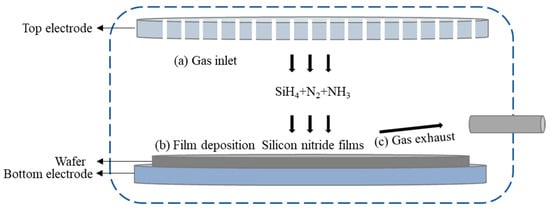
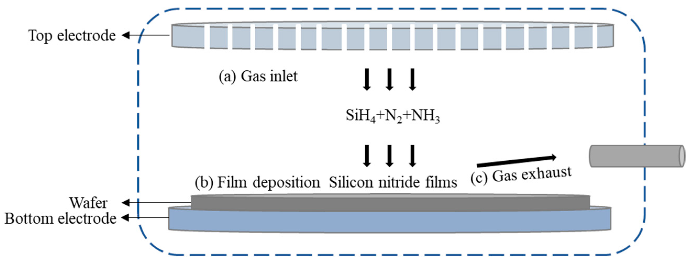
In this study, silicon nitride films were deposited using commercial PECVD equipment. The purity of the N2, SiH4, and NH3 gases utilized exceeded 99.99%. The 12-inch (100) silicon wafer was used for film deposition. As shown in Figure 1, the schematic diagram of the PECVD system, gas enters the chamber through the top electrode. Under the RF electric field, silicon nitride films are deposited on the wafer placed on the bottom electrode, while the residual gas is exhausted through the exhaust pipe. Both the top and bottom electrodes have circular surfaces. Based on our team’s previous research experience, the baseline deposition parameters for the silicon nitride films are detailed in Table 1. Furthermore, to analyze the impact of the NH3 precursor on film properties and its RF response mechanism, two sets of single-variable experiments were designed involving RF power (300, 400, 500, 600, 700, 800, and 900 W) and electrode gap (13, 14, 15, 16, 17, 18, and 19 mm). Deposition rates varied across different conditions, so the deposition time was adjusted accordingly to keep all films in this study at around 2000 Å in thickness.
Figure 1.
Schematic diagram of PECVD of silicon nitride films.
Table 1.
Baseline deposition parameters for silicon nitride films.
2.2. Characterization Methods
Deposition rate: The deposition rate was defined as the thickness of the film deposited per unit time. The film thickness was measured using an Aleris 8500 (KLA Tencor) instrument, with six wafers tested for each film type. The thickness was measured using spectroscopic ellipsometry over a wavelength range of 300–800 nm. The optical model was based on the Cauchy dispersion model, and the data were fitted using the least-squares method. The uncertainty in film thickness measurements was less than 1%. The calculation formula for the deposition rate was given by Equation (1). THK is the average of six wafers, and t is the deposition time.
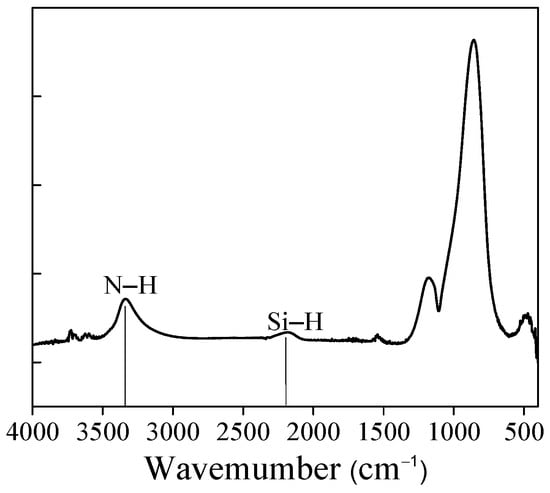
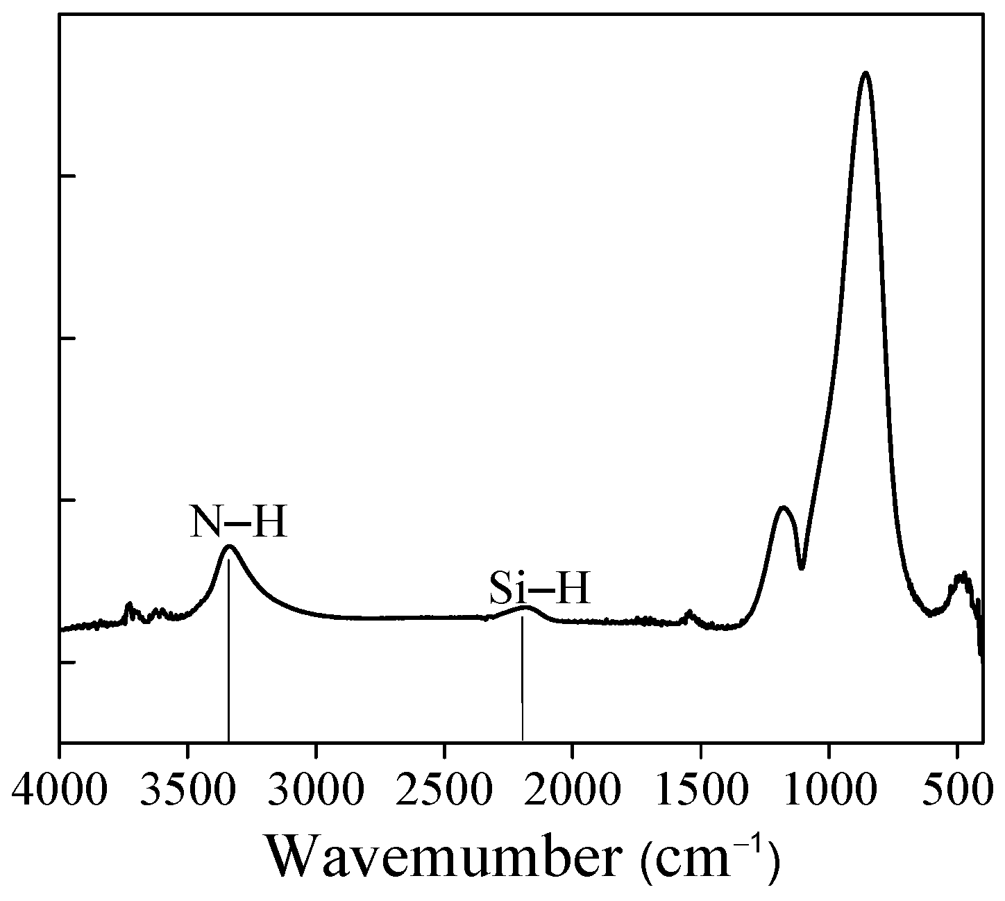
Chemical bonds: To probe the internal chemical bonds, the films were analyzed by FT-IR spectroscopy in the 400–4000 cm−1 range. The measurement was performed in attenuated total reflectance mode. The Lanford–Rand method [20], recommended by Thermo Scientific, was applied based on the Si–H and N–H peaks. As shown in Figure 2, the peaks at 2190 cm−1 and 3342 cm−1 were assigned to Si–H and N–H bonds, respectively [21]. Based on Equations (2) and (3), the number of Si–H (ASi–H) and N–H (AN–H) bonds per unit volume in the film can be calculated. The concentrations of Si–H and N–H bonds, denoted as CSi–H and CN–H, are then derived from Equations (4) and (5), respectively. Subsequently, the total content (CH) and ratio (RH) of Si–H to N–H bonds were determined from Equations (6) and (7) [22]. Meanwhile, the Si/N atomic ratio of the films was determined using X-ray photoelectron spectroscopy (Nexsa G2, Thermo Fisher Scientific, Waltham, MA, USA). The etching process was performed for 30 s with an ion beam energy of 50 eV.
where HSi–H and HN–H are the peak heights of Si–H and N–H bonds.
Figure 2.
FT-IR spectra of silicon nitride films deposited from SiH4/N2/NH3 system.
Non-uniformity: The thickness non-uniformity was also measured using an Aleris 8500 (KLA Tencor) instrument and evaluated using Equation (8) based on 49-point measurements. σTHK and μTHK are the standard deviation and average value of thickness, respectively.
Surface roughness and morphology: The surface of the film was observed using scanning electron microscopy (SEM). The surface roughness of the silicon nitride films was quantitatively characterized using a Bruker Dimension Icon atomic force microscope (AFM). All measurements were performed under ambient conditions at room temperature in tapping mode, with a scan area of 2 μm × 2 μm and a scan rate of 2 Hz. The arithmetic average roughness (Ra) was automatically calculated using the instrument’s built-in NanoScope Analysis software to ensure consistency and reproducibility in data processing.
Refractive index: The refractive index was characterized with an Aleris 8500 (KLA, Milpitas, CA, USA) instrument. For each film type, measurements were performed on six wafers, and the final value was taken as the average.
Stress: The stress of silicon nitride films was measured using a T910 system (Skyverse, Shenzhen, China), with six wafers tested for each film type. The film stress was calculated based on the change in the wafer curvature radius before and after deposition, according to the Stoney equation given in Formula (9).
where σ is the film stress, Es and νs are the Young’s modulus and Poisson’s ratio of the substrate, respectively. ts is the substrate thickness, tf is the film thickness, and Rs and Rf are the curvature radii before and after deposition, respectively.
3. Results and Discussion
3.1. Deposition Rate
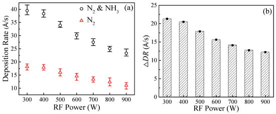
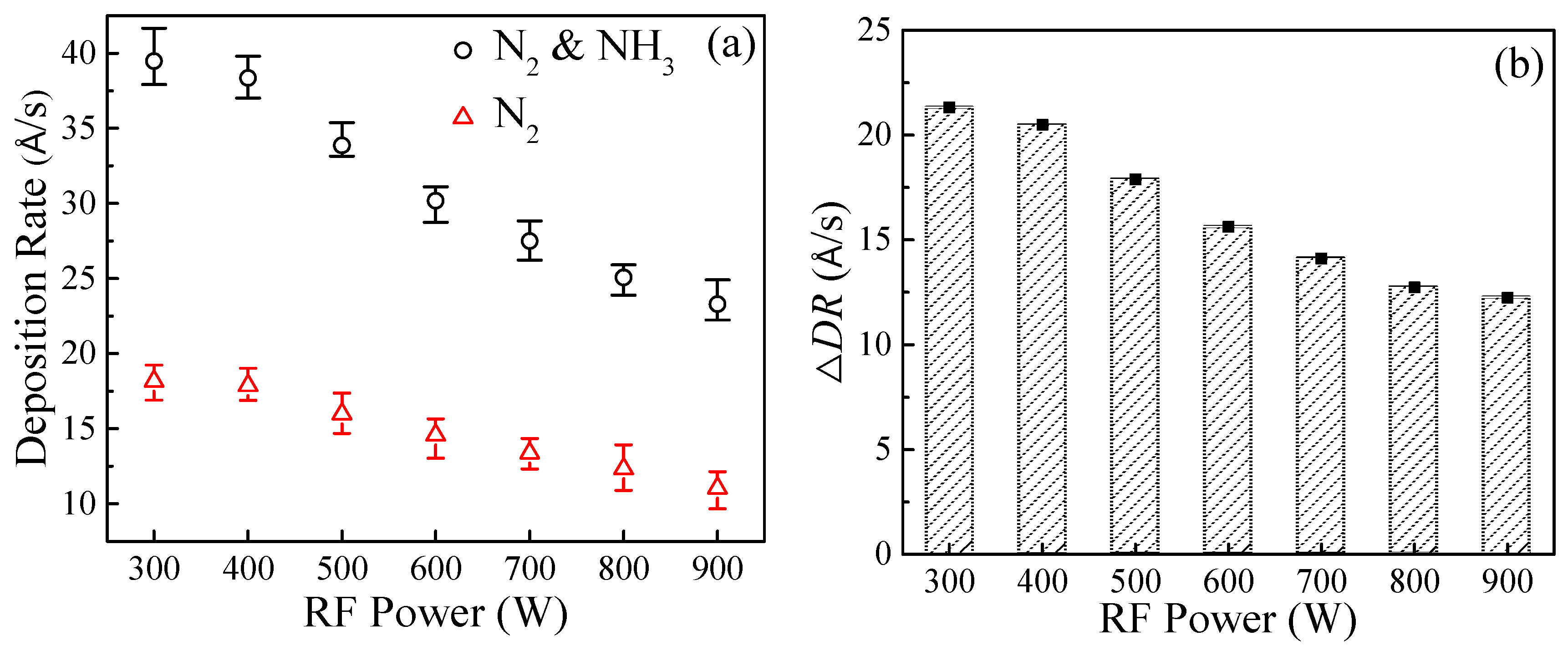
Figure 3a illustrates the variation in deposition rate with RF power under different precursor systems. A significant enhancement in the deposition rate is observed with the introduction of NH3: at 300 W, a deposition rate of 39.5 Å/s is achieved by the SiH4/NH3/N2 system, which is approximately 117% higher than that obtained with the pure N2 system. From the perspective of molecular physics, the bond energy of N2 (945 kJ/mol) is substantially higher than that of NH3 (391 kJ/mol), resulting in a higher dissociation barrier [23]. In contrast, NH3 is more readily subjected to stepwise dissociation, generating highly reactive NHx radicals. These radicals are characterized by a significantly higher sticking coefficient on the substrate surface when compared to atomic nitrogen, thereby effectively accelerating the film growth kinetics. Furthermore, as the RF power is increased from 300 W to 900 W, a monotonic decline in the deposition rates is exhibited by both systems. This trend is attributed to an “ion bombardment-induced densification” process: higher power leads to the kinetic energy of ions being enhanced, whereby micropores in the film are compacted through an atomic peening effect [24,25]. Consequently, the mass per unit volume is increased, which is macroscopically manifested as a slowdown in the growth rate.
Figure 3.
(a) Dependence of the deposition rate on RF power for the two silicon nitride film systems; (b) Effect of NH3 introduction on the silicon nitride films deposition rate.
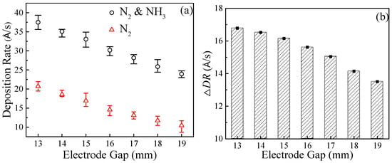
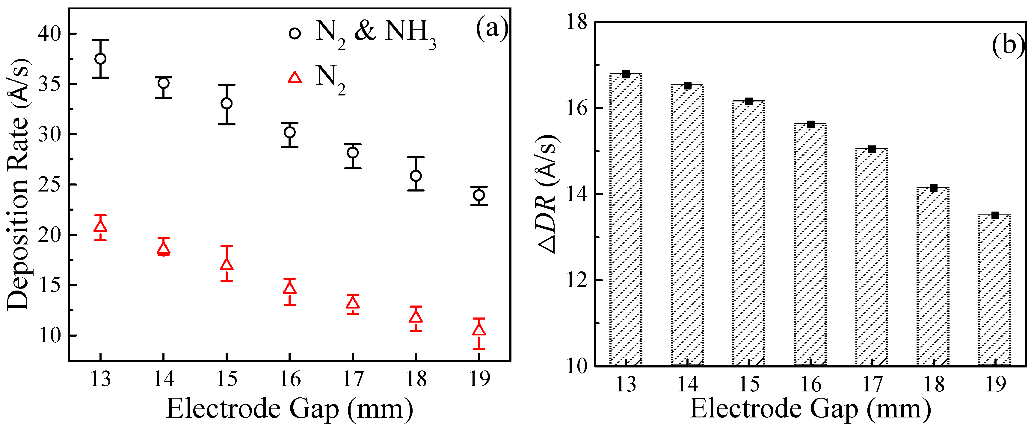
The effects of different system and electrode gap on the deposition rate of silicon nitride films are examined in Figure 4. As shown in Figure 4a, a gradual decrease in the deposition rate is observed with increasing electrode gap. This trend is noted for both the SiH4/N2 and SiH4/NH3/N2 systems. Specifically, with the increase in gap from 13 mm to 19 mm, the deposition rate is reduced from 20.7 Å/s to 10.4 Å/s in the N2 system. In the NH3/N2 system, a decrease from 37.5 Å/s to 23.9 Å/s is observed. This decrease is mainly due to the larger electrode gap. The increased gap weakens the RF electric field strength. Consequently, the ionization efficiency of the reaction gases is reduced [26].
Figure 4.
(a) Dependence of the deposition rate on electrode gap for the two silicon nitride film systems; (b) Effect of NH3 introduction on the silicon nitride film deposition rate.
Overall, in the plasma environment, the dissociation energy of NH3 is significantly lower than that of N2, enabling more efficient generation of high concentrations of reactive nitrogen radicals. As shown in Figure 3b and Figure 4b, the deposition rate of the NH3-added system is consistently maintained significantly higher than that of the pure N2 system. Meanwhile, through analysis of the deposition rate difference with and without NH3 (ΔDR), it is concluded that this kinetic advantage provided by NH3 is strongly modulated by plasma parameters and exhibits convergence with changes in system energy or spatial density. On one hand, as the RF power is increased, the enhancement in deposition rate due to NH3 shows a slow decay. This indicates that the high-power environment supplies enough energy to N2 molecules with high bond energy, resulting in a compensatory increase in their dissociation efficiency [27]. Consequently, the gap in active species flux between the two nitrogen sources is narrowed. On the other hand, the gain effect of NH3 is also weakened with increasing electrode gap. Under small gap conditions, the strong electric field and high plasma density between the electrodes fully amplify the advantage of NH3’s easier dissociation. However, as the gap is expanded, the electric field strength and plasma density are generally reduced. This leads to a suppression of precursor dissociation probability, thereby diminishing the inherent reactivity difference between the two nitrogen sources.
3.2. Chemical Bonds
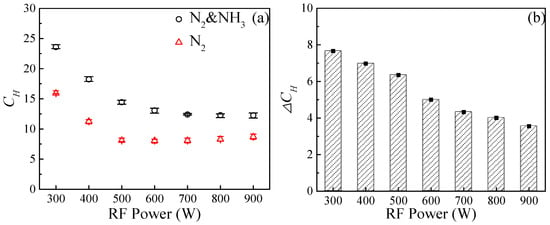
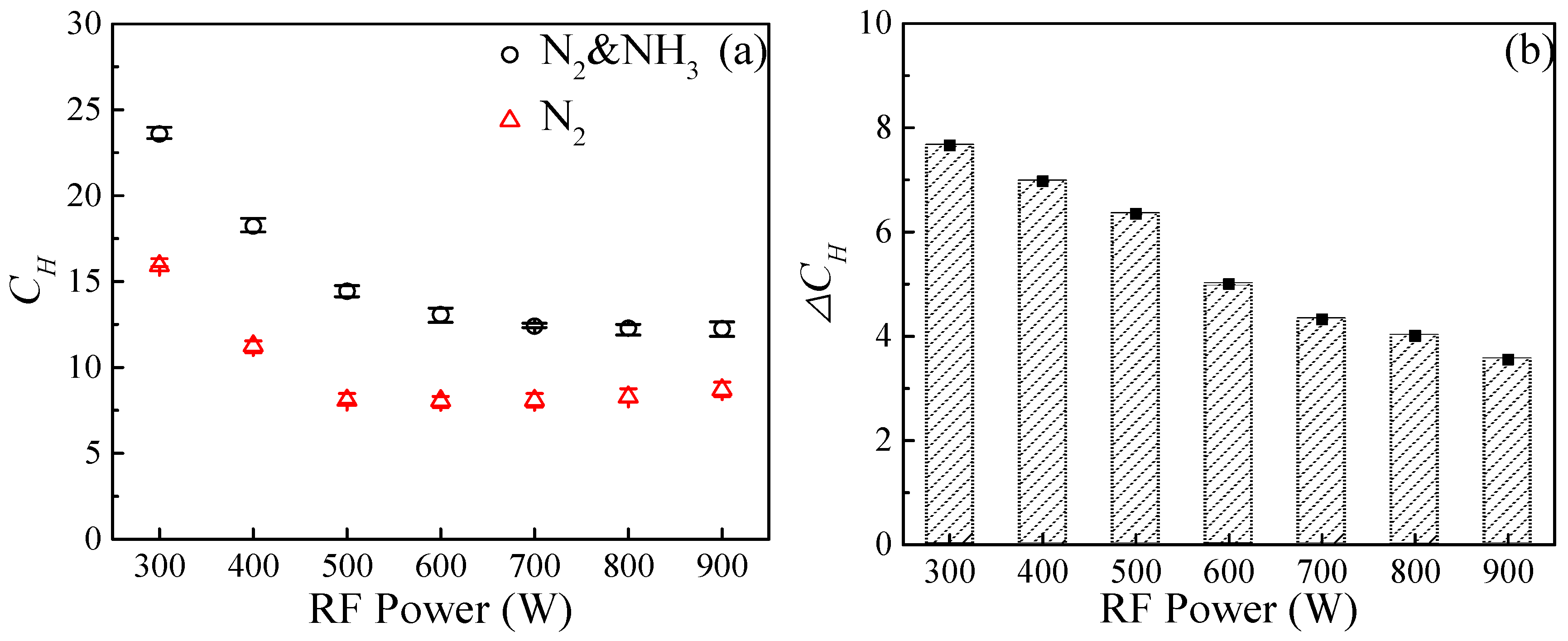
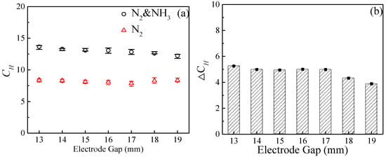
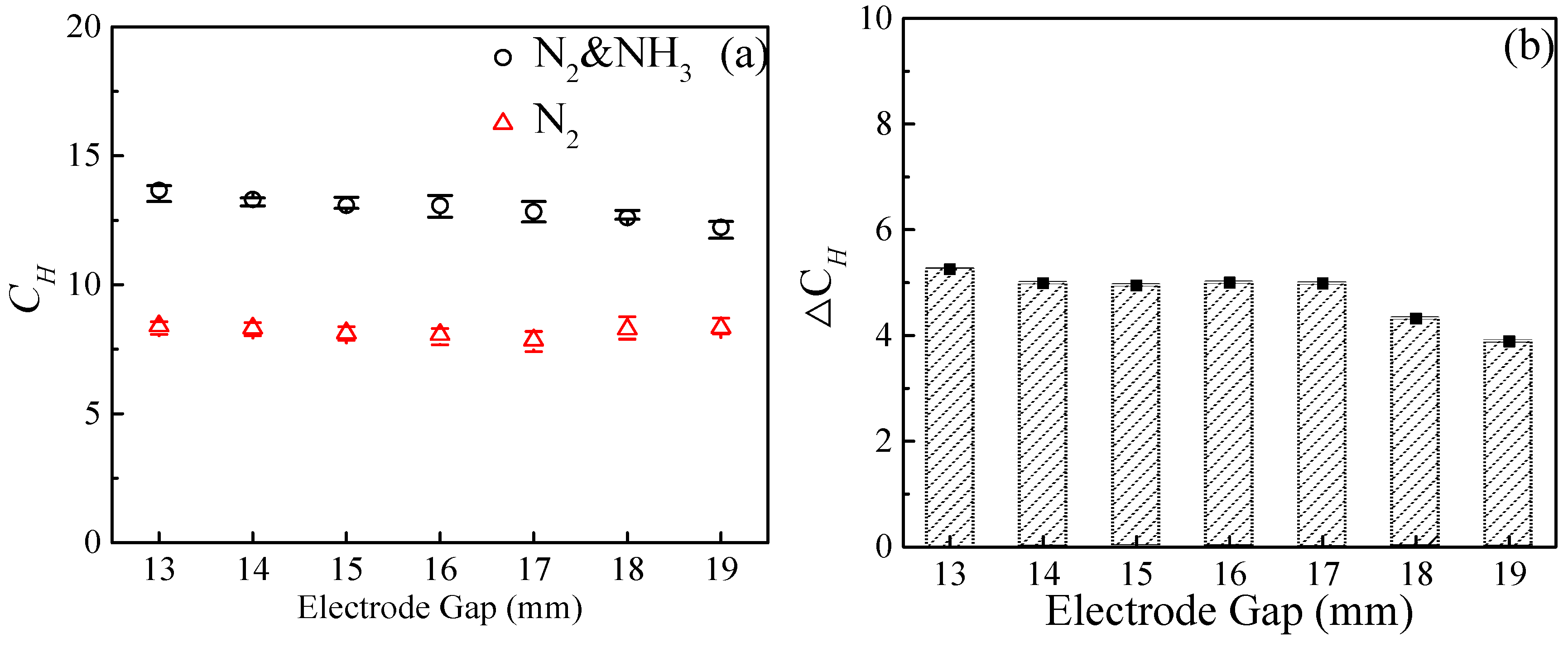
Figure 5a shows the variation in total hydrogen content (CH) in silicon nitride films with RF power and electrode gap under different nitrogen precursor systems. The CH of the film decreases significantly with increasing power, regardless of NH3 introduction. When the power is raised from 300 W to 900 W, the CH of the SiH4/NH3/N2 system decreases from 23.58% to 12.25%, while that of the SiH4/N2 system decreases from 15.93% to 8.70%. The underlying mechanism lies in the enhanced energy coupling of the plasma at high power, which promotes deeper precursor dissociation and provides adsorbed atoms on the growing surface with higher kinetic energy, thereby accelerating dehydrogenation during film formation [28]. Meanwhile, as shown in Figure 6a, as the gap increases from 13 mm to 19 mm, the CH of the SiH4/NH3/N2 system decreases from 13.65% to 12.22%, and the CH of the NH3-containing system shows a slight decreasing trend. This is mainly because a larger gap allows for more spatial diffusion of the reaction gases. It also prolongs the residence time of active species in the chamber. Both factors facilitate dehydrogenation reactions in the gas phase and on the surface. In contrast, the SiH4/N2 system is less affected by the gap variation. Its CH remains lower than that of the NH3-containing system across the entire process range. This lower CH reflects the direct contribution of NH3 dissociation to N–H bonding groups in the film.
Figure 5.
(a) Dependence of the CH on RF power for the two silicon nitride film systems; (b) Effect of NH3 introduction on the silicon nitride films CH.
Figure 6.
(a) Dependence of the CH on electrode gap for the two silicon nitride film systems; (b) Effect of NH3 introduction on the silicon nitride films CH.
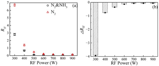
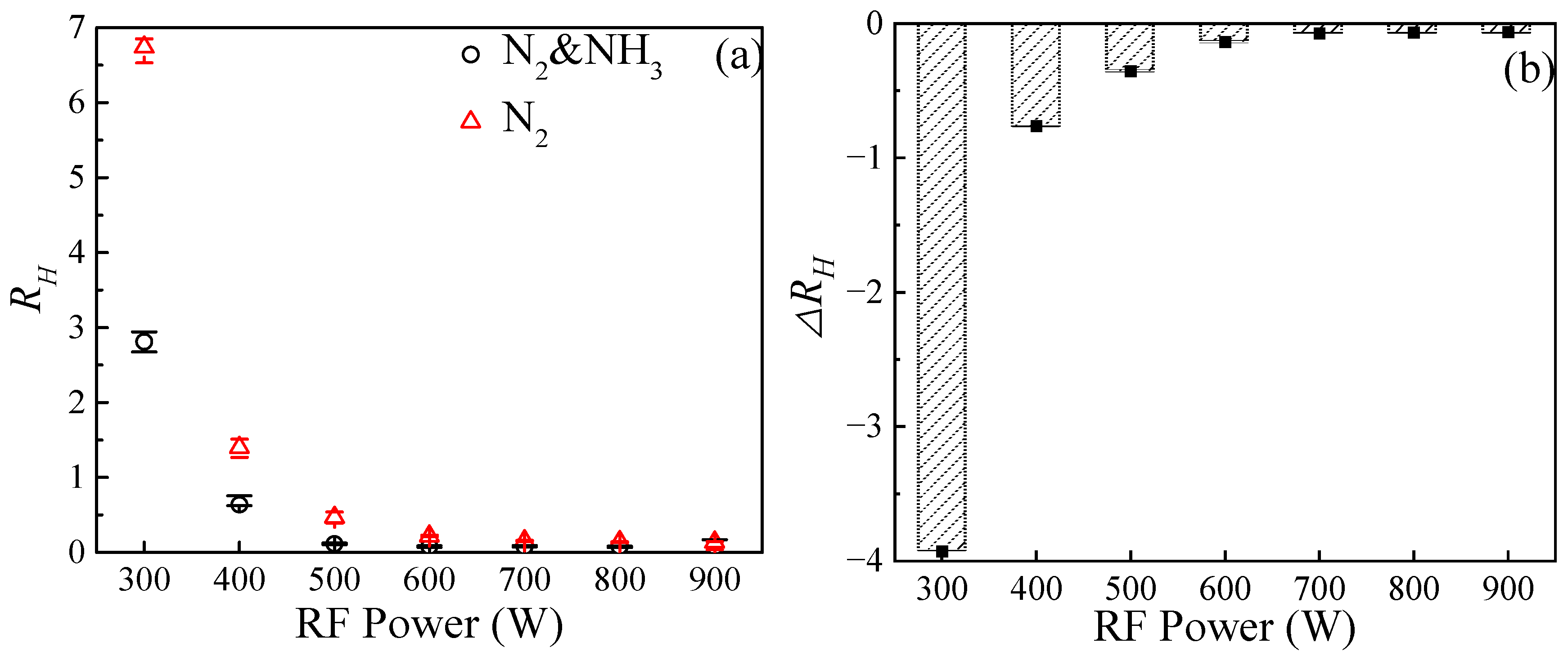
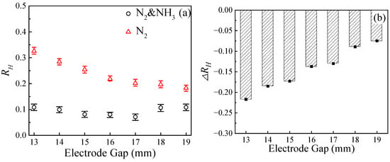
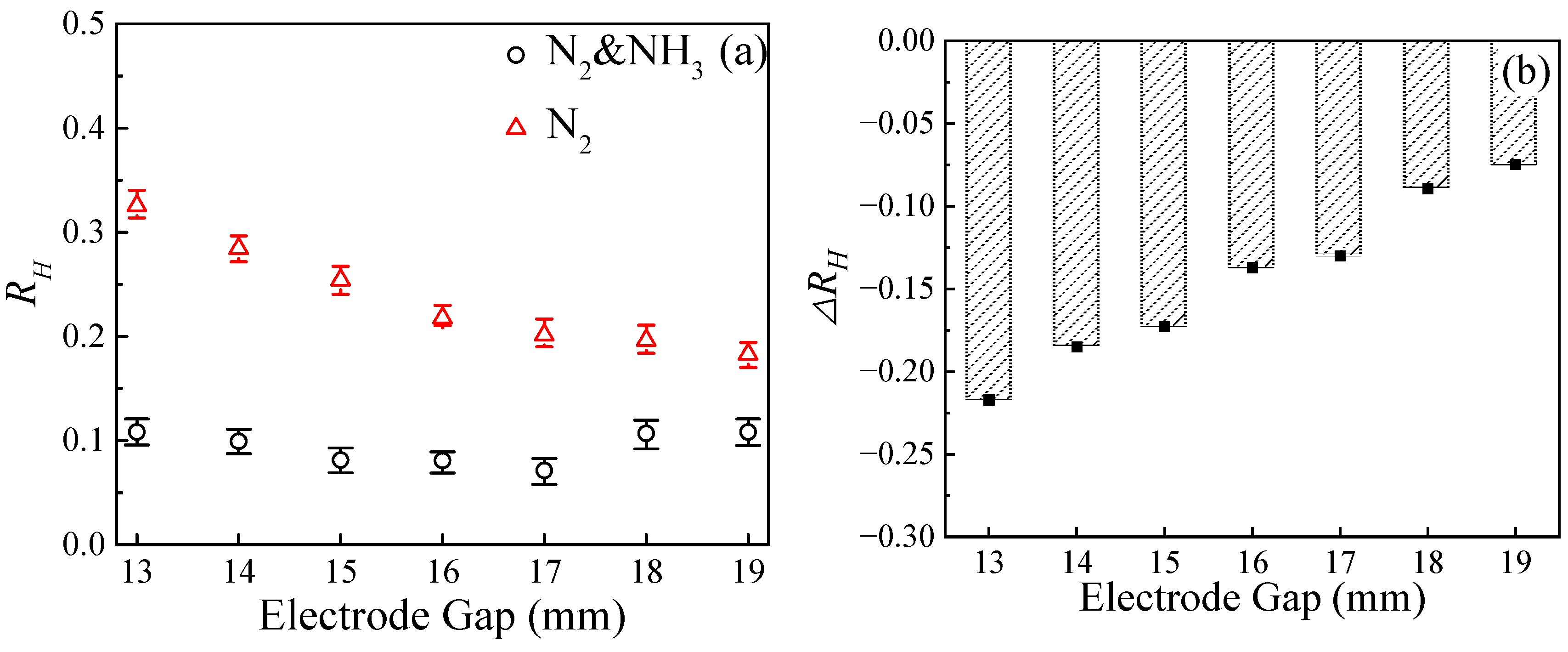
The evolution of the Si–H/N–H atomic ratio (RH) in the film is further shown in Figure 7a. At an RF power of 600 W, the RH is significantly reduced from 0.22 to 0.08 with the introduction of NH3, compared to the pure SiH4/N2 system. This reduction is attributed to the lower bond dissociation energy of NH3, which allows reactive nitrogen species to be generated more efficiently than from the chemically stable N2 molecule. In terms of response characteristics, the RH in both systems exhibits a monotonic decreasing trend as the power increases. This confirms the beneficial effect of enhanced nitrogen dissociation efficiency under high-energy conditions on the bonding structure. Additionally, as shown in Figure 8a, an increase in electrode gap provides more opportunities for gas-phase collisions and diffusion in the NH3-containing system, leading to a slight decrease in the RH with a larger gap. In contrast, due to the high dissociation energy threshold of N2, the SiH4/N2 system shows negligible compositional fluctuation when the spatial distribution is altered, demonstrating strong stability against gap variation.
Figure 7.
(a) Dependence of the RH on RF power for the two silicon nitride film systems; (b) Effect of NH3 introduction on the silicon nitride films RH.
Figure 8.
(a) Dependence of the RH on electrode gap for the two silicon nitride film systems; (b) Effect of NH3 introduction on the silicon nitride films RH.
To further quantify the contribution of NH3 in the film-forming reaction, ΔCH and ΔRH between the two systems with and without NH3 were shown in Figure 5b and Figure 7b, respectively. The influence of NH3 addition is shown to be highly dependent on the RF power. At low RF power (300 W), N2 molecules are difficult to be effectively activated by the plasma. Under this condition, NH3 becomes the primary active nitrogen source. Many NHx radicals are directly supplied. ΔCH and ΔRH are 7.68% and −3.93, respectively. As the RF power increases to 900 W, both ΔCH and ΔRH show a clear narrowing trend. ΔCH and ΔRH are 3.56% and −0.07, respectively. The reason is that the dissociation barrier of N2 is overcome by the high-energy plasma, thereby compensating for the insufficient supply of active nitrogen in the NH3-free system. Meanwhile, dehydrogenation reactions on the growing surface are enhanced by intense ion bombardment, which effectively removes the excess hydrogen atoms introduced by NH3. ΔCH and ΔRH between the two systems with and without NH3 were shown in Figure 6b and Figure 8b, respectively. Compared to RF power, the electrode gap has a gentler effect on ΔCH and ΔRH. An increase in the electrode gap from 13 mm to 19 mm resulted in a decrease in ΔCH from 5.25% to 3.89% and a change in ΔRH from −0.22 to −0.07.
From the perspective of plasma dynamics, an increased electrode gap results in a reduced local electric field strength. However, the residence time and mean free path of gas molecules in the reaction chamber are significantly extended. For the easily dissociable NH3, enough dissociation is maintained through secondary collisions, even under a weakened electric field, due to the extended residence time. In contrast, for the SiH4/N2 system, the dissociation energy barrier of N2 cannot be substantially overcome by merely altering the spatial distribution and collision probability of particles. Consequently, the supply of active nitrogen from NH3 is consistently more stable than that from N2 across different electrode gaps. Thus, the chemical bond differences between the two systems are largely desensitized to variations in the spatial scale.
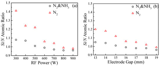
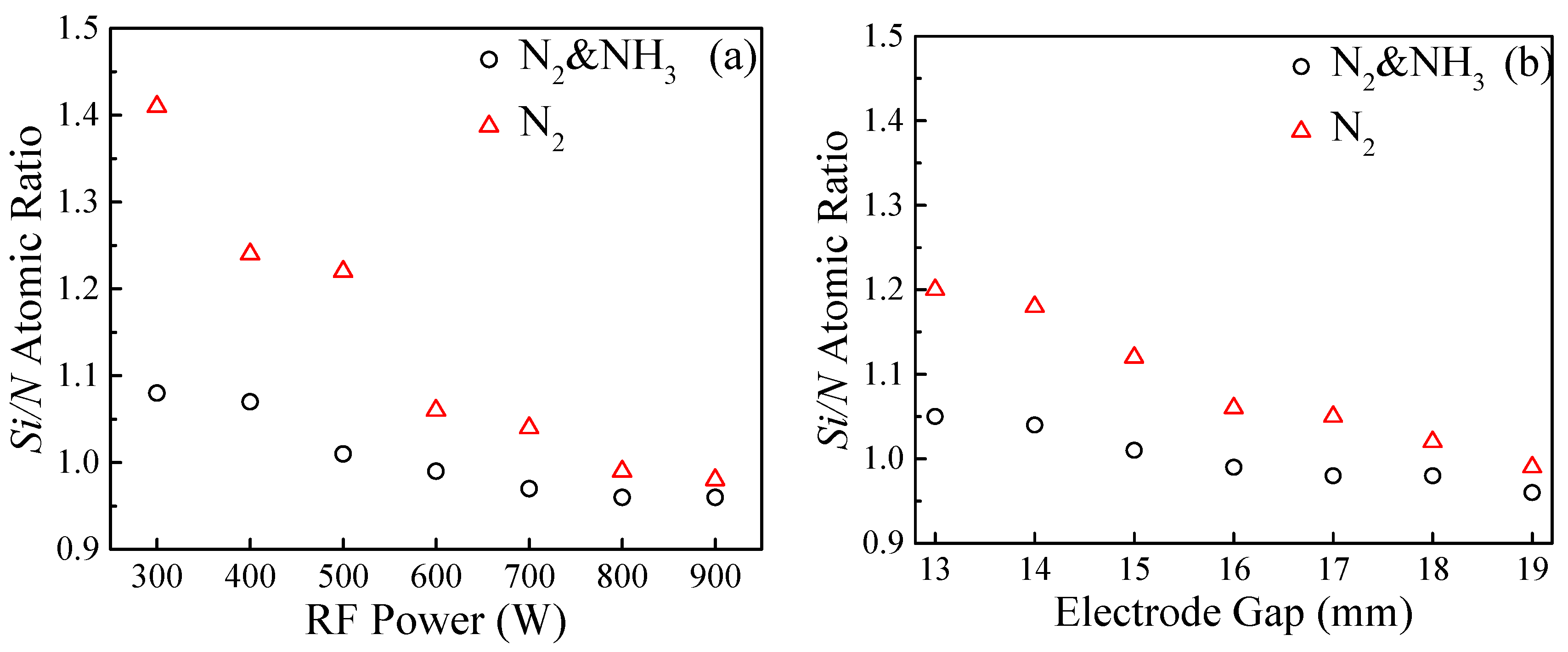
The influence of RF power and electrode gap on the Si/N atomic ratio of the deposited films is shown in Figure 9. From Figure 9a, it is observed that when the RF power was increased from 300 W to 900 W, the Si/N ratio of the SiH4/N2/NH3 system decreased from 1.41 to 0.98. The Si/N ratio of the SiH4/N2 system was decreased from 1.08 to 0.96. From the standpoint of plasma reaction kinetics, SiH4 can be dissociated. In contrast, N2 molecules contain a strong nitrogen–nitrogen triple bond. This is difficult to break. At lower RF powers, N2 dissociation is insufficient. Therefore, the films are enriched with Si. As the RF power is increased, the density of high-energy electrons in the plasma is increased sharply. Consequently, the dissociation rate of N2 through inelastic collisions is greatly enhanced. A rapid rise in the concentration of reactive nitrogen radicals is caused. As a result, a significant drop in the Si/N ratio is observed. Meanwhile, the bond energy of NH3 is lower than that of the N2. Therefore, NH3 is dissociated much more readily at low power levels. A plentiful nitrogen source is provided. By introducing NH3, the film Si/N ratio is lowered considerably. At a high power of 900 W, however, the system energy is high enough. N2 is decomposed efficiently and thoroughly. Under such conditions, the concentration of active nitrogen precursors in both systems is brought to saturation. The final Si/N atomic ratios are quite similar.
Figure 9.
The influence of (a) RF power and (b) electrode gap on the Si/N atomic ratio.
On the other hand, it is indicated in Figure 9b that when the electrode gap was increased from 13 mm to 19 mm, the Si/N ratio of the SiH4/N2/NH3 system was decreased from 1.20 to 0.99. The Si/N ratio of the SiH4/N2 system was decreased from 1.05 to 0.96. This is mainly attributed to the fact that a larger electrode gap is used. The plasma discharge region is extended. The residence time of the reactive gases in the glow zone is prolonged. With a longer residence time, the chance of high-energy electrons colliding with the relatively inert N2 molecules is improved. The conversion of N2 into reactive species is made more effective. As a result, the proportion of available nitrogen in the gas phase is increased. The Si/N atomic ratios in both systems are decreased with increasing electrode gap.
3.3. Non-Uniformity
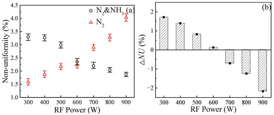
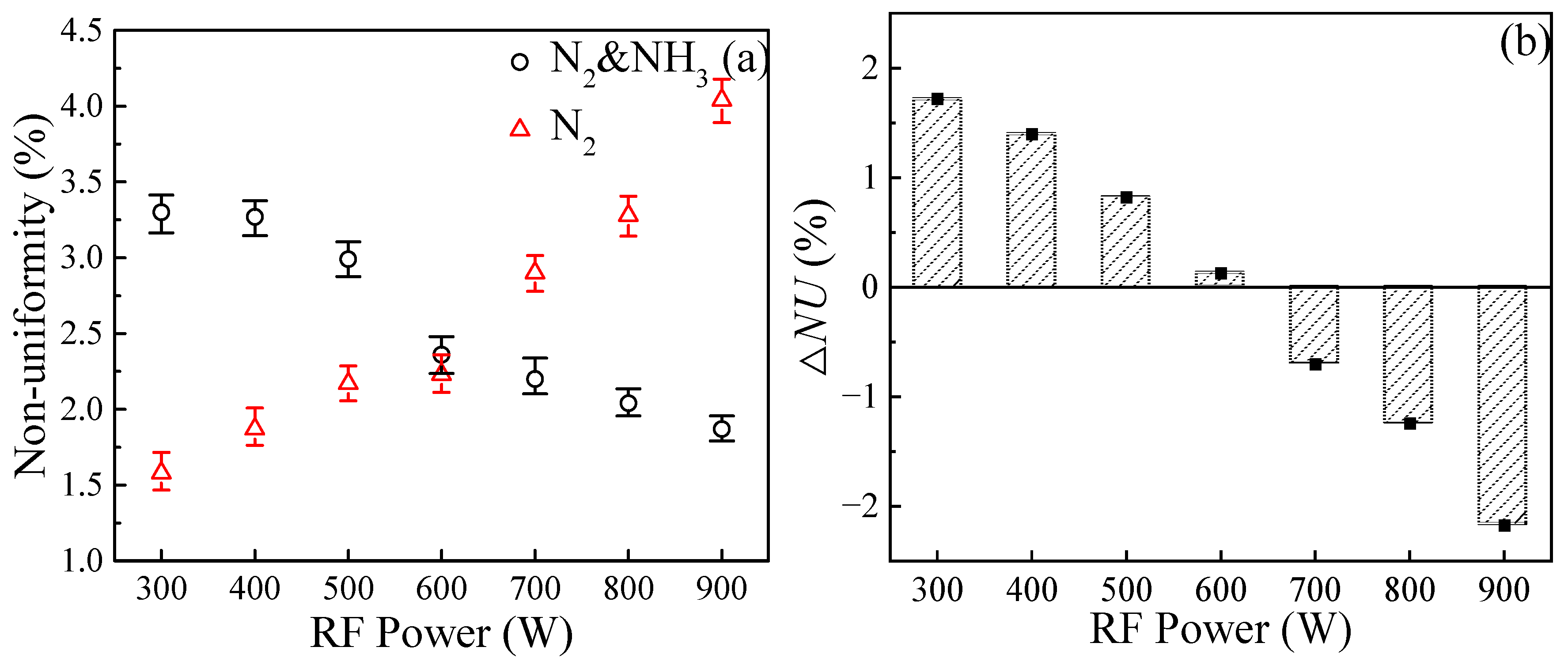
Figure 10a illustrates the thickness non-uniformity of silicon nitride films as a function of RF power under different nitrogen precursor systems. In general, a film non-uniformity below 2% is acceptable for customer specifications. As the RF power was raised from 300 W to 900 W, sharply divergent responses in film uniformity were observed between the two precursor systems. In the SiH4/NH3/N2 system, the non-uniformity was significantly improved from 3.30% to 1.87%, which can meet customer requirements. By contrast, a marked deterioration was shown by the pure N2 system, with the non-uniformity worsening from 1.58% to 4.04%. This difference is attributed to the lower bond energy of NH3, which allows its dissociation efficiency to be effectively enhanced at high power, resulting in the release of a high flux of active nitrogen radicals. Consequently, a more uniform species distribution is formed in the chamber, promoting spatial consistency in the deposition reaction. In comparison, the bond energy of the N2 molecule is much higher than that of NH3. Under high-power excitation, the plasma is concentrated predominantly in the central electrode region. This asymmetric distribution of the electric field leads to an increased flux difference in active nitrogen between the center and edge of the electrode, ultimately causing an unbalanced thickness distribution of the film [29].
Figure 10.
(a) Dependence of the NU on RF power for the two silicon nitride film systems; (b) Effect of NH3 introduction on the silicon nitride films NU.
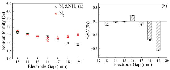
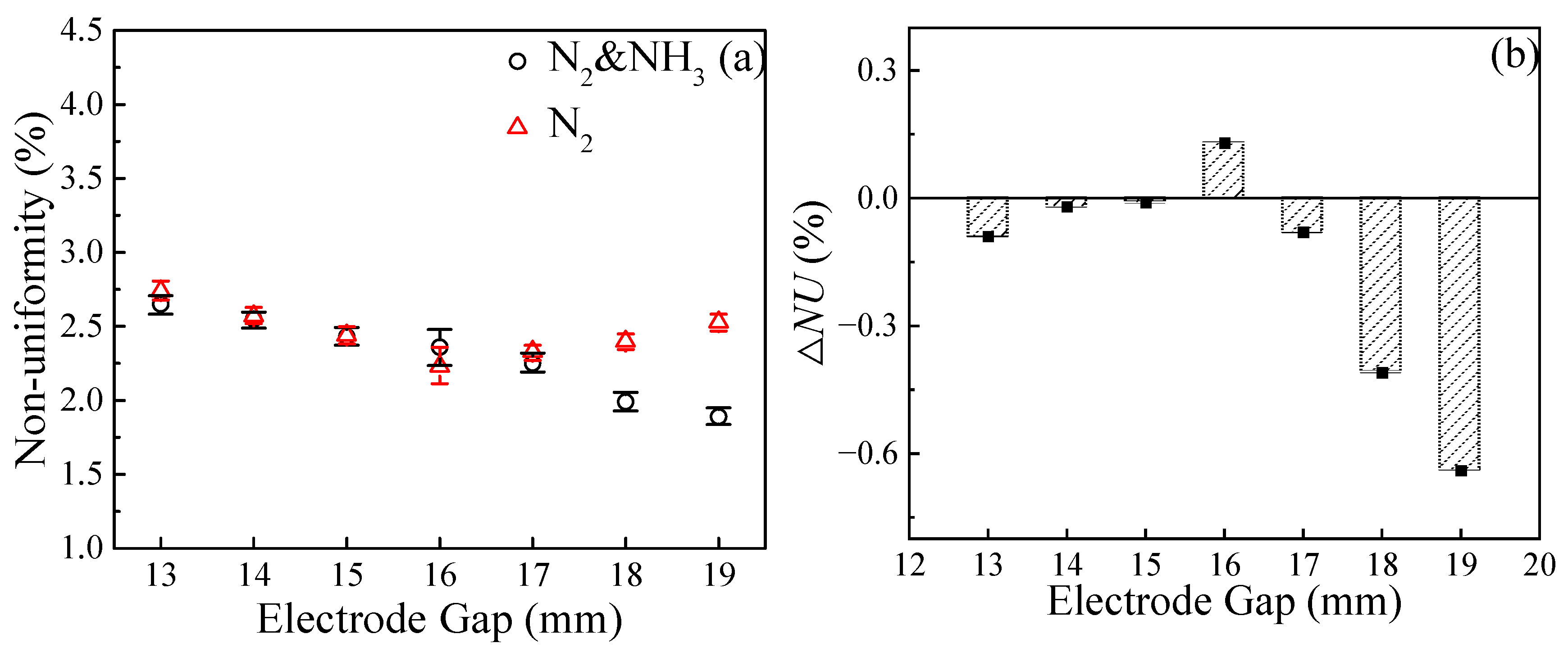
Figure 11a compares the response of film non-uniformity to changes in the electrode gap distance. As the gap is increased from 13 mm to 19 mm, a continuous improvement in film uniformity is observed for the SiH4/NH3/N2 system, with the value decreasing from 2.65% to 1.89%. In contrast, the SiH4/N2 system exhibits a non-monotonic variation: uniformity first improves and then deteriorates as the gap widens. This difference is attributed to the introduction of NH3, which significantly increases the concentration of active nitrogen species in the plasma. As a result, the film deposition process becomes less sensitive to local electric field variations. In addition, a larger gap increases the mean free path of the reaction gases. This promotes better diffusion and a more uniform distribution of active species [30]. In the SiH4/N2 system, however, the concentration of active species is lower, and their distribution is less uniform. Therefore, film uniformity becomes highly dependent on a specific optimal gap, corresponding to a narrow process window. Any deviation from this gap leads to rapid degradation in uniformity.
Figure 11.
(a) Dependence of the NU on electrode gap for the two silicon nitride film systems; (b) Effect of NH3 introduction on the silicon nitride films NU.
Figure 10b and Figure 11b further quantify the effect of NH3 on film uniformity by comparing the uniformity difference (ΔNU) with and without NH3. The influence of NH3 is found to be jointly affected by RF power and gap. At low power (300 W), incomplete dissociation of NH3 increases plasma complexity, negatively affecting uniformity. However, above 600 W, full dissociation of NH3 stabilizes the plasma, leading to significantly improved uniformity. Across all gap distances, uniformity is generally improved with NH3. At a 19 mm gap, the uniformity value is reduced by 0.64%, indicating a clear enhancement. Thus, by introducing NH3 under high-power and large-gap conditions, the non-uniform plasma distribution in pure N2 systems can be effectively overcome, enabling high-level film uniformity.
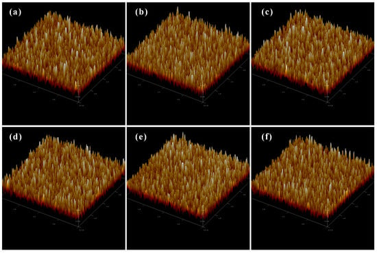
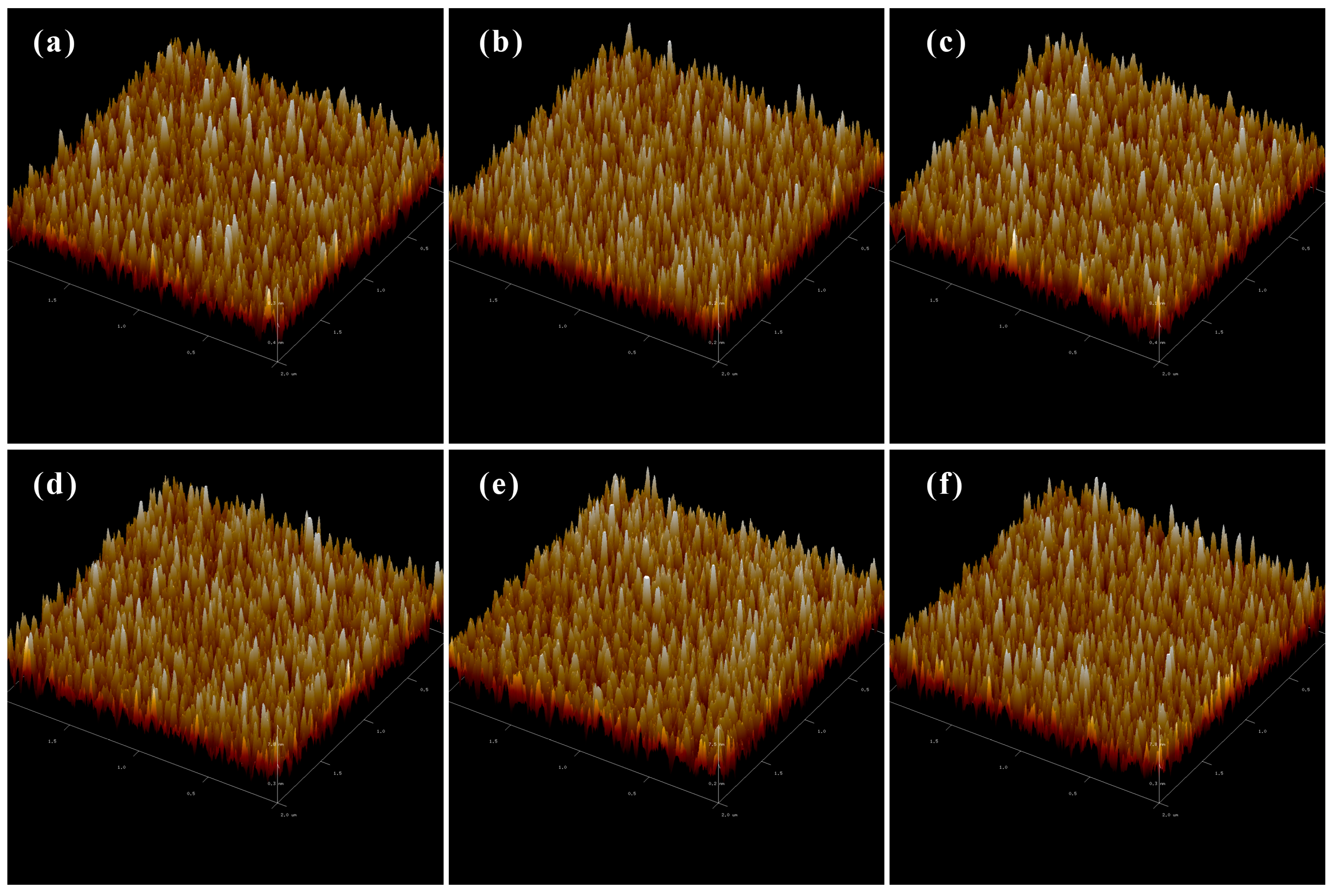
As shown in Figure 12, AFM was used to characterize the surface roughness of films prepared under different RF power and electrode gap conditions. Overall, no significant change in surface roughness was caused by varying the electric field parameters. When the RF power was increased from 600 W to 900 W, the macroscopic non-uniformity was raised from 2.23% to 4.04%. The Rₐ was only slightly increased, from 2.21 nm to 2.28 nm. When the electrode gap was increased from 16 mm to 19 mm, the non-uniformity was raised to 2.53%. The Rₐ was kept almost unchanged, at around 2.20 nm. From these results, it is suggested that changes in RF power and electrode gap mainly affect the spatial distribution of the plasma inside the reaction chamber. The macroscopic uniformity of the film is therefore altered by this effect. On the other hand, the microscopic roughness is more dependent on how reactive radicals move on the substrate surface and how nucleation happens locally. A strong effect from the macroscopic electric field fluctuations is not seen at this level. The sample phenomenon can also be observed in the SiH4/N2/NH3 system. Under the same increases in power and gap, the non-uniformity of the film was significantly reduced from 2.36% to 1.87% and 1.89%. At the same time, the roughness was only slightly changed within a narrow range, from 2.16 to 2.11 or 2.14. Overall, the non-uniformity is mainly controlled by adjusting the electric field parameters. However, only a very limited effect on the local roughness is produced by these adjustments.
Figure 12.
AFM images of silicon nitride films under different conditions: (a,b) SiH4/N2 and SiH4/N2/NH3 systems, RF power 600 W, gap 16 mm; (c,d) same as above, RF power 900 W, gap 16 mm; (e,f) same as above, RF power 600 W, gap 19 mm.
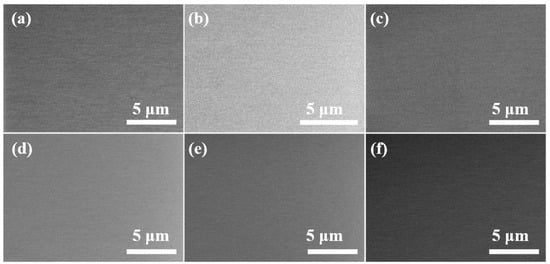
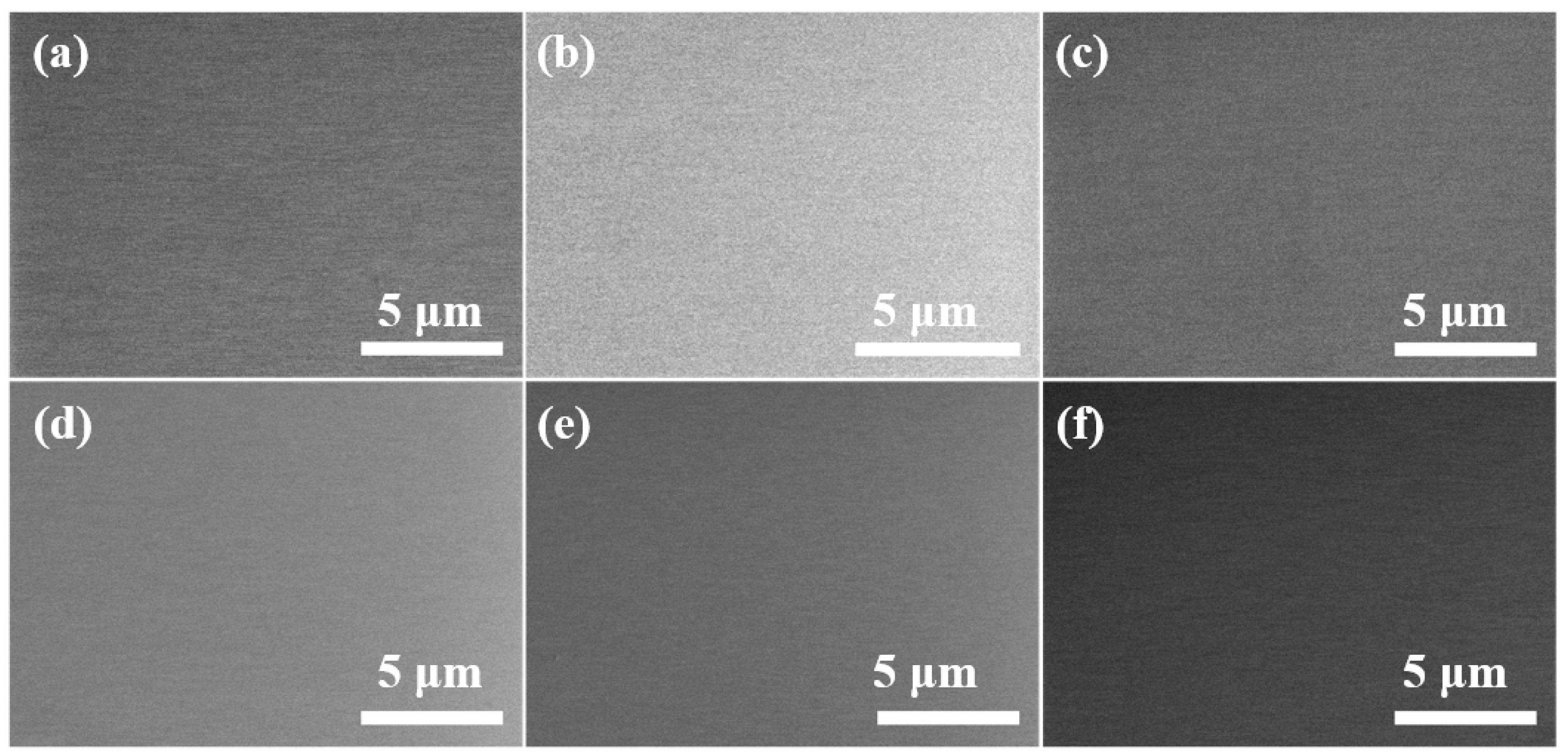
To further evaluate the quality of the films, SEM was used to characterize the samples prepared under different process conditions (Figure 13). The results showed that highly continuous and flat microscopic morphologies were obtained in all conditions. No physical defects such as microcracks, holes, or local delamination were observed. It is worth noting that even when the residual compressive stress in the film reached as high as −989.7 MPa under certain parameters, the film still maintained good quality. This phenomenon indicates that the films deposited in this system possess high intrinsic mechanical stability. The internal high strain energy can be effectively accommodated. At the same time, good interfacial adhesion between the film and the substrate was formed. The buckling or delamination effects that are commonly caused by high compressive stress were successfully suppressed. In summary, it is confirmed that although the internal stress state of the film is significantly changed by adjusting the electric field parameters, the structural integrity is not damaged. The deposited films always maintain good process reliability.
Figure 13.
(a) SEM images of silicon nitride films under different conditions: (a,b) SiH4/N2 and SiH4/N2/NH3 systems, RF power 600 W, gap 16 mm; (c,d) same as above, RF power 900 W, gap 16 mm; (e,f) same as above, RF power 600 W, gap 19 mm.
3.4. Refractive Index
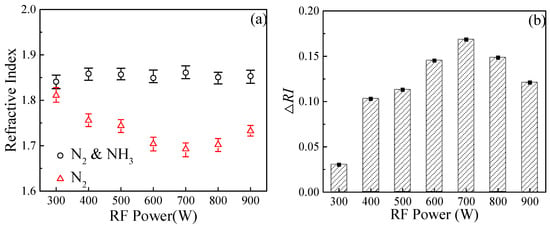
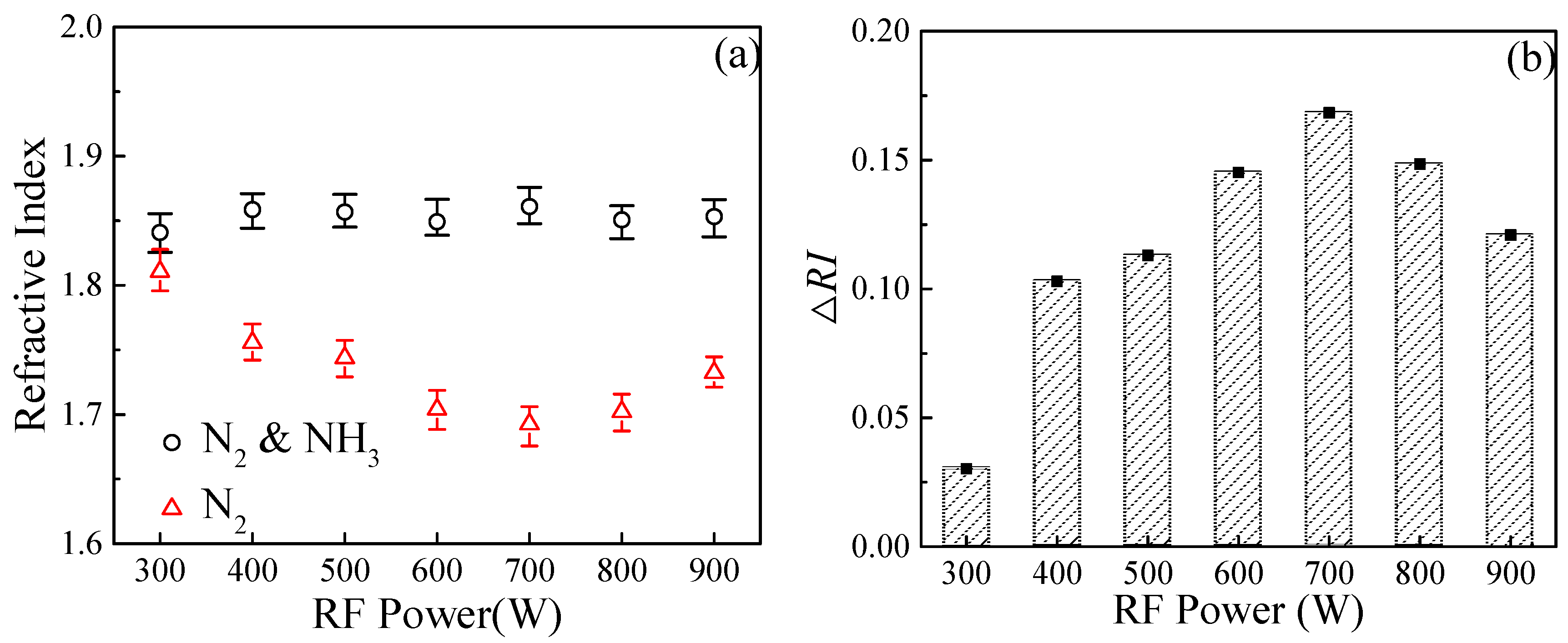
As shown in Figure 14, the RF power was increased from 300 W to 900 W. No significant change was observed in the refractive index of films deposited from the SiH4/N2/NH3 system. In contrast, a decrease followed by an increasing trend was exhibited by the SiH4/N2 system. The refractive index of silicon nitride films is generally dominated by the Si/N atomic ratio [31]. With increasing RF power, the Si/N ratio of the SiH4/N2/NH3 system was not significantly changed. Therefore, its refractive index remained relatively stable. For the SiH4/N2 system, a clear decreasing trend was observed in the Si/N ratio. As a result, the refractive index initially decreased. However, when the RF power exceeded 700 W, an abnormal increase in the refractive index was observed in the SiH4/N2 system. This can be attributed to the fact that at high power levels, the dissociation efficiency of N2 molecules was greatly improved. Intense ion bombardment caused the increase in film density to become the dominant factor [32]. Thus, the overall refractive index was raised. Accordingly, the overall refractive index of the NH3-added system was higher than that of the pure N2 system. This was also attributed to the higher film density of the SiH4/N2/NH3 system compared to the SiH4/N2 system.
Figure 14.
(a) Dependence of the RI on RF power for the two silicon nitride film systems; (b) Effect of NH3 introduction on the silicon nitride films RI.
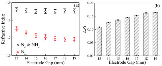
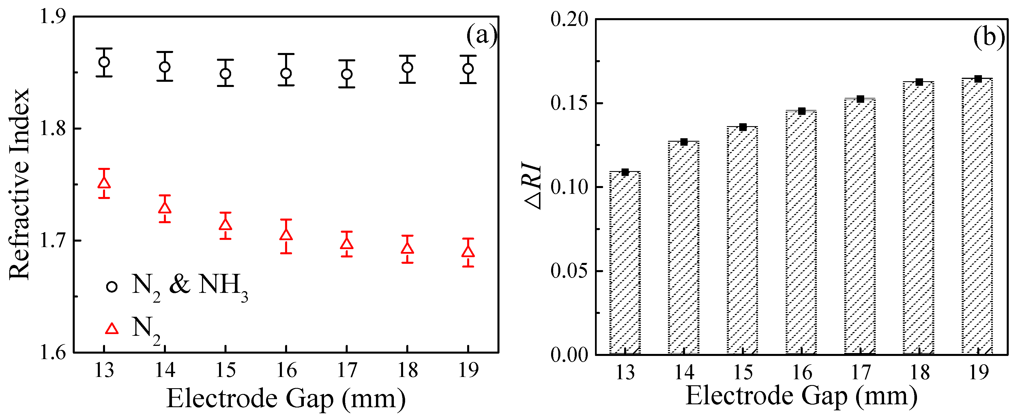
The influence of electrode gap on film refractive index is shown in Figure 15. As illustrated in Figure 15a, the refractive index of the SiH4/N2/NH3 system was highly insensitive to variations in the electrode gap. It remained stable at approximately 1.85. In contrast, as the electrode gap was increased from 13 mm to 19 mm, a monotonic decrease in refractive index from 1.75 to 1.69 was observed in the pure N2 (SiH4/N2) system. This trend was consistent with the previously observed change in film Si/N ratio with increasing gap. It was further confirmed that the refractive index was mainly determined by the Si/N atomic ratio, when it was not affected by strong densification effects.
Figure 15.
(a) Dependence of the RI on electrode gap for the two silicon nitride film systems; (b) Effect of NH3 introduction on the silicon nitride films RI.
3.5. Stress
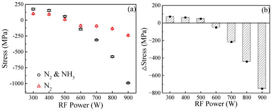
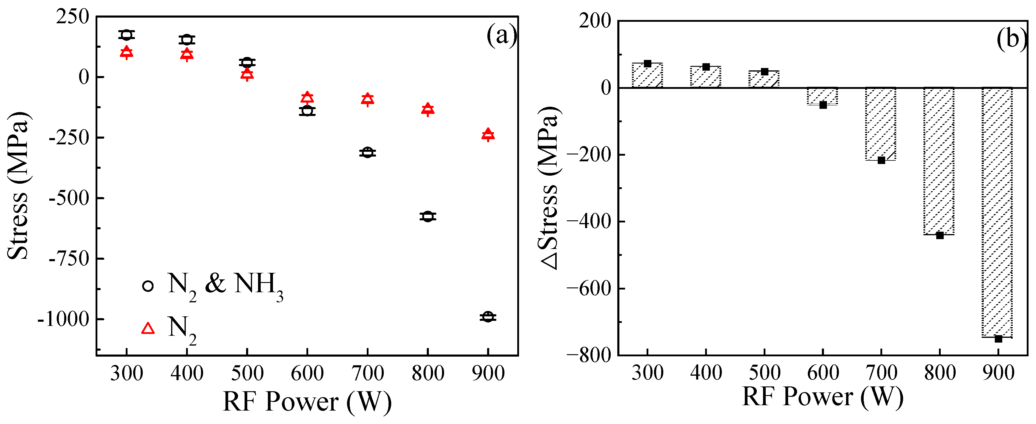
The evolution of stress with RF power for silicon nitride films deposited using different nitrogen precursor systems is shown in Figure 16a. As the RF power increases from 300 W to 900 W, the stress in both types of film transitions from a tensile to a compressive state. Specifically, the stress in the SiH4/NH3/N2 system changes gradually from 100.7 MPa to −239.03 MPa, while that of the SiH4/N2 system exhibits a more pronounced shift, decreasing from 173.3 MPa to −989.7 MPa. This stress transition behavior is consistent with that observed under conventional deposition conditions at 400 °C [33]. The underlying mechanism lies in the enhanced ion bombardment effect on the growing film surface at higher RF powers, which induces a densification reorganization of the internal film structure, thereby driving the macroscopic stress toward a compressive state [34,35,36].
Figure 16.
(a) Dependence of the stress on RF power for the two silicon nitride film systems; (b) Effect of NH3 introduction on the silicon nitride films stress.
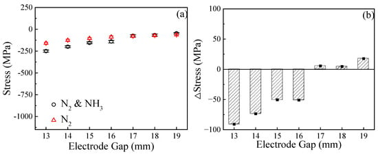
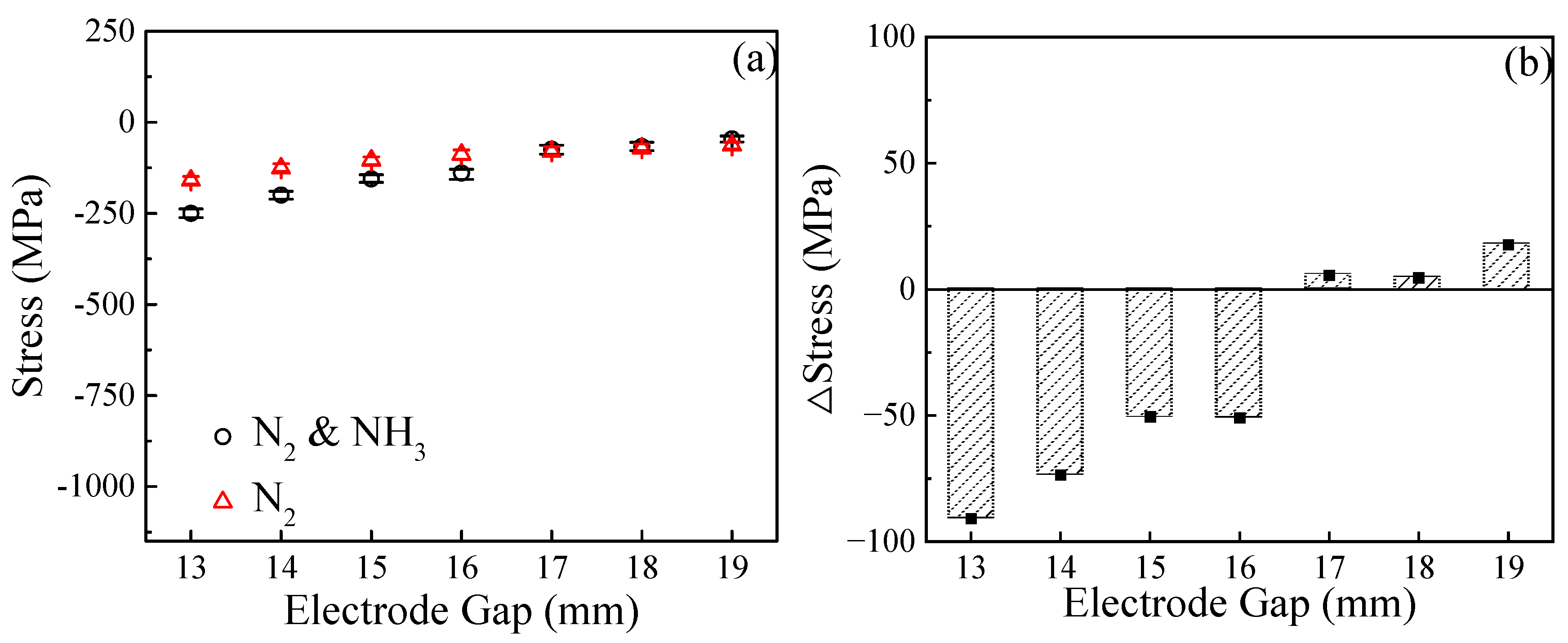
As shown in Figure 17a, the stress in the SiH4/NH3/N2 system shifts toward tension as the electrode gap increases from 13 mm to 19 mm, with the stress value changing from −250.13 MPa to −45.58 MPa. This trend is attributed to the reduced electric field strength at larger gaps, which leads to an increase in hydrogen content and consequently promotes tensile stress characteristics [37]. Similarly, when pure N2 is employed as the nitrogen precursor, the film stress increases from 159.3 MPa to −63.3 MPa as the gap widens.
Figure 17.
(a) Dependence of the stress on electrode gap for the two silicon nitride film systems; (b) Effect of NH3 introduction on the silicon nitride films stress.
To further quantify the specific impact of NH3 introduction on film stress, the differential stress curves between the two precursor systems are provided in Figure 16b and Figure 17b. The stress response is defined by a threshold at 600 W. Introduction of NH3 below this power results in a slight increase in tensile stress, whereas above it, the compressive stress is markedly enhanced, with an increment reaching 750.65 MPa at 900 W. A critical point is identified at an electrode gap of 16 mm. When the gap is below 16 mm, the addition of NH3 enhances compressive stress; in contrast, beyond 16 mm, it promotes tensile stress. This transition is dictated by the electric field energy (a combined function of power and gap).
Under high power or small gap conditions, NH3 is effectively dissociated, providing abundant active nitrogen species. At the same time, intense ion bombardment promotes the formation of a highly densified Si–N network. These factors together lead to a significant increase in compressive stress. In contrast, under low power or large gap conditions, NH3 dissociation is incomplete. As a result, more Si–H and N–H bonds are incorporated into the film. In addition, weaker ion bombardment results in a relatively porous film structure. The combination of these effects ultimately increases the macroscopic tensile stress.
4. Conclusions
To overcome the limitations of low-temperature deposition, this study investigated the PECVD process for silicon nitride films using SiH4/NH3/N2 and SiH4/N2 reaction systems and successfully established an optimization methodology and theoretical framework. Specifically, compared with the SiH4/N2 system, the introduction of NH3 played a key role in accelerating the deposition rate. At 300 W, the rate increased by 117% to 39.5 Å/s, due to its higher efficiency in generating reactive nitrogen radicals. However, adding NH3 also increased the hydrogen content in the films and affected spatial uniformity. The study showed that increasing RF power can effectively reduce hydrogen content. When the power was raised from 300 W to 900 W, the dissociation efficiency improved significantly, and the hydrogen content dropped from 23.58% to 12.25%. Meanwhile, the changes in plasma energy and spatial characteristics greatly improved film uniformity in the SiH4/N2/NH3 system. Increasing the RF power from 300 W to 900 W reduced non-uniformity from 3.30% to 1.87%, and expanding the electrode gap from 13 mm to 19 mm further reduced it from 2.65% to 1.89%. Finally, by balancing these interacting parameters, this study provides a clear and practical process window for industrial mass production.
Author Contributions
Z.T.: Conceptualization, Writing—Original Draft, Writing—Review and Editing, Data Curation; P.Y.: Resources, Data Curation, Writing—Review and Editing; Y.Q.: Writing—Review and Editing; Z.W.: Methodology, Data Curation; J.N.: Investigation, Project Administration; Z.R.: Writing—Review and Editing. All authors have read and agreed to the published version of the manuscript.
Funding
This research received no external funding.
Data Availability Statement
The data presented in this study are available upon request from the corresponding author.
Conflicts of Interest
Authors Zhen Tang, Peng Yu, Yanli Qi, Zhuo Wang and Jianping Ning were employed by the Piotech, Inc. The remaining authors declare that the research was conducted in the absence of any commercial or financial relationships that could be construed as a potential conflict of interest.
References
- Rathinavelu, V.; Upadhyay, V.V.; Prabagaran, S.; Govindarajan, S.; Verma, A.; Soudagar, M.E.M.; Vinayagam, M.; Alotaibi, M.A.; Seikh, A.H. Texturing of silicon nitride passivation layers on functional behaviour study of polycrystalline silicon (p-Si) made with plasma enhanced chemical vapour deposition. J. Mater. Sci.-Mater. Electron. 2025, 36, 73. [Google Scholar] [CrossRef] [Scilit]
- Zhang, Y.H.; Li, J.Y.; Peng, H.; Yang, H.; Lu, L.; Zhang, S.D. Investigation of passivation layers for self-aligned top-gate amorphous InGaZnO thin-film transistors with metal-reacted low-resistance source/drain. In Proceedings of 2025 9TH IEEE Electron Devices Technology & Manufacturing Conference, EDTM; IEEE: New York, NY, USA, 2025. [Google Scholar]
- Kempf, E.; Calvo, M.; Domengie, F.; Monfray, S.; Orobtchouk, R. Low Temperature SiN Waveguides Optimization for Photonic Platform. In 2020 22nd International Conference on Transparent Optical Networks (ICTON); IEEE: New York, NY, USA, 2020. [Google Scholar]
- Taka, H.; Suzuki, K.; Tsujioka, N.; Murakami, S. Development of high-quality low-temperature PECVD-SiN films by organosilane. In 2015 International 3D Systems Integration Conference (3DIC); IEEE: New York, NY, USA, 2015. [Google Scholar]
- Ghosh, M.; Bulkin, P.; Silva, F.; Johnson, E.V.; Florea, I.; Funes-Hernando, D.; Tanguy, A.; Renard, C.; Vaissiere, N.; Decobert, J. Ultrathin Ge epilayers on Si produced by low-temperature PECVD acting as virtual substrates for III-V/c-Si tandem solar cells. Sol. Energy Mater. Sol. Cells 2022, 236, 111535. [Google Scholar]
- Holmes, M.R.; Liu, S.; Keeley, J.; Jenkins, M.; Hawkins, A.R. Hollow Waveguides With Low Intrinsic Photoluminescence Fabricated With PECVD Silicon Nitride and Silicon Dioxide Films. IEEE Photonics Technol. Lett. 2011, 23, 1466–1468. [Google Scholar] [CrossRef] [Scilit]
- Lai, T.L.; Lee, Y.F.; Hsu, Y.H.; Tsai, C.P.; Huang, C.K.; Liu, C.Y. Low-temperature PECVD silicon-nitride passivation for perovskite solar cell. Mater. Chem. Phys. 2022, 294, 126880. [Google Scholar]
- Martyniuk, M.; Antoszewski, J.; Musca, C.A.; Dell, J.M.; Faraone, L. Environmental stability and cryogenic thermal cycling of low-temperature plasma-deposited silicon nitride thin films. J. Appl. Phys. 2006, 99, 567. [Google Scholar] [CrossRef] [Scilit]
- Meitine, M.; Sazonov, A. Low Temperature PECVD Silicon Oxide For Devices And Circuits On Flexible Substrates. MRS Proc. 2003, 769, 66. [Google Scholar] [CrossRef] [Scilit]
- Huang, W.D.; Wang, X.H.; Sheng, M.; Xu, L.Q.; Stubhan, F.; Luo, L.; Feng, T.; Wang, X.; Zhang, F.M.; Zou, S.C. Low temperature PECVD SiNx films applied in OLED packaging. Mater. Sci. Eng. B-Solid State Mater. Adv. Technol. 2003, 98, 248–254. [Google Scholar] [CrossRef] [Scilit]
- Domínguez Bucio, T.; Khokhar, A.Z.; Lacava, C.; Stankovic, S.; Mashanovich, G.Z.; Petropoulos, P.; Gardes, F.Y. Material and optical properties of low-temperature NH3-free PECVD SiNx layers for photonic applications. J. Phys. D. Appl. Phys. A Europhys. J. 2017, 50, 025106. [Google Scholar]
- Alamgeer; Yousuf, H.; Khokhar, M.Q.; ur Rahman, R.; Chu, M.; Aida, M.N.; Madara, P.C.; Jony, J.A.; Jang, S.; Bae, J.; et al. Enhanced field-assisted passivation and optical properties improvement of PECVD deposited SiNx:H thin film. Opt. Lett. 2025, 162, 116885. [Google Scholar] [CrossRef] [Scilit]
- Jehanathan, N. Thermal Stability of Plasma Enhanced Chemical Vapor Deposition Silicon Nitride Thin Films. Master’s Thesis, The University of Western Australia, Crawley, WA, Australia, 2007. [Google Scholar]
- Murata, T.; Miyagawa, Y.; Isaki, R.; Shibata, T.; Matsuda, R.; Tsujiuchi, M.; Takeuchi, Y.; Ueno, S.; Matsuura, M.; Asai, K. Effect of NH3-Free Silicon Nitride for Protection Layer of Magnetic Tunnel Junction on Magnetic Properties of Magnetoresistive Random Access Memory. Jpn. J. Appl. Phys. 2009, 48, 04C024. [Google Scholar] [CrossRef] [Scilit]
- Ahn, S.; Hong, S.J.; Yang, H.S.; Cho, S.M. Effect of 2 MHz frequency power applied to the substrate for low-temperature silicon nitride thin film deposition. Mater. Sci. Semicond. Process. 2022, 143, 106538. [Google Scholar] [CrossRef] [Scilit]
- Oh, S.J.; Ma, B.S.; Yang, C.; Kim, T.S. Intrinsic Mechanical Properties of Free-Standing SiNx Thin Films Depending on PECVD Conditions for Controlling Residual Stress. ACS Appl. Electron. Mater. 2022, 4, 3980–3987. [Google Scholar]
- Iliescu, C.; Tay, F.E.H.; Wei, J. Low stress PECVD—SiNx layers at high deposition rates using high power and high frequency for MEMS applications. J. Micromech. Microeng. 2006, 16, 869–874. [Google Scholar]
- Li, W.; Kang, Z.; Ye, Y.; Jiang, Y. Influences of process parameters of low frequency PECVD technology on intrinsic stress of silicon nitride thin film. In 5th International Symposium on Advanced Optical Manufacturing and Testing Technologies: Optoelectronic Materials and Devices for Detector, Imager, Display, and Energy Conversion Technology; SPIE: Bellingham, DC, USA, 2010. [Google Scholar]
- Loboda, M.J.; Seifferly, J.A. Chemical influence of inert gas on the thin film stress in plasma-enhanced chemical vapor deposited a-SiN: H films. J. Mater. Res. 1996, 11, 391–398. [Google Scholar] [CrossRef] [Scilit]
- Lanford, W.A.; Rand, M.J. The hydrogen content of plasma-deposited silicon nitride. J. Appl. Phys. 1978, 49, 2473–2477. [Google Scholar] [CrossRef] [Scilit]
- Watanabe, T.; Hori, K.; Habuka, H. Anticorrosive Behavior of SiCxNyOz Film Formed by Non-Heat Assistance Plasma-Enhanced Chemical Vapor Deposition Using Monomethylsilane, Nitrogen and Argon Gases. ECS J. Solid State Sci. Technol. 2020, 9, 024001. [Google Scholar] [CrossRef] [Scilit]
- Arifuku, N.; Jin, H.; Jeon, M.S.; Dhamrin, M.; Suda, M.; Saitoh, T.; Kamisako, K.; Hirasawa, T.; Eguchi, T.; Yamaga, I. Characteristic Evaluation of SiNx: H Films Passivation Effect on Ga-doped Multi-crystalline Silicon Wafers. In 2006 IEEE 4th World Conference on Photovoltaic Energy Conference; IEEE: New York, NY, USA, 2006; pp. 1287–1290. [Google Scholar]
- Xu, X.; He, Q.; Fan, T.; Jiang, Y.; Huang, L.; Ao, T.; Ma, C. Hard and relaxed a-SiNxHy films prepared by PECVD: Structure analysis and formation mechanism. Appl. Surf. Sci. 2013, 264, 823–831. [Google Scholar] [CrossRef] [Scilit]
- Kim, B.; Kim, J.; Uh, H.S. Radio Frequency Power Effect on Charge Density of PECVD-SiN Thin Films. J. Ceram. Soc. Jpn. 2007, 115, 772–775. [Google Scholar]
- Lee, M.-J.; Kar, J.P.; Lee, T.I.; Lee, D.; Choi, D.-K.; Cho, J.-H.; Myoung, J.-M. Investigation of optical and compositional properties of thin SiNx:H films with an enhanced growth rate by high frequency PECVD method. Vacuum 2011, 85, 1032–1036. [Google Scholar] [CrossRef] [Scilit]
- Ning, J.; Tang, Z.; Chen, L.; Li, B.; Wu, Q.; Sun, Y.; Zhou, D. Impact of H-related chemical bonds on physical properties of SiNx: H Films deposited via plasma-enhanced chemical vapor deposition. Electronics 2024, 13, 2779. [Google Scholar]
- Sahu, B.B.; Shin, K.S.; Han, J.G. Integrated approach for low-temperature synthesis of high-quality silicon nitride films in PECVD using RF–UHF hybrid plasmas. Plasma Sources Sci. Technol. 2016, 25, 015017. [Google Scholar] [CrossRef] [Scilit]
- Zhao, L.; Zhang, W.; Chen, J.; Diao, H.; Wang, Q.; Wang, W. Plasma enhanced chemical vapor deposition of excellent a-Si:H passivation layers for a-Si:H/c-Si heterojunction solar cells at high pressure and high power. Front. Energy 2017, 11, 85–91. [Google Scholar] [CrossRef] [Scilit]
- Herth, E.; Desré, H.; Algré, E.; Legrand, C.; Lasri, T. Investigation of optical and chemical bond properties of hydrogenated amorphous silicon nitride for optoelectronics applications. Microelectron. Reliab. 2012, 52, 141–146. [Google Scholar] [CrossRef] [Scilit]
- Kim, K.S.; Kim, K.H.; Ji, Y.J.; Park, J.W.; Shin, J.H.; Ellingboe, A.R.; Yeom, G.Y. Silicon Nitride Deposition for Flexible Organic Electronic Devices by VHF (162 MHz)-PECVD Using a Multi-Tile Push-Pull Plasma Source. Sci. Rep. 2017, 7, 13585. [Google Scholar] [CrossRef] [Scilit] [PubMed]
- Guler, I. Characterization of N Rich-Silicon Nitride Thin Films Deposited by PECVD. ECS J. Solid State Sci. Technol. 2023, 12, 046002. [Google Scholar] [CrossRef] [Scilit]
- Yang, L.-Q.; Zhang, C.; Li, W.-L.; Liu, G.-H.; Wu, M.; Liu, J.-Q.; Zhang, J.-H. Global optimization of process parameters for low-temperature SiNx based on orthogonal experiments. Adv. Manuf. 2023, 11, 181–190. [Google Scholar] [CrossRef] [Scilit]
- Kang, Z.; Li, Y.; Yuan, K.; Jiang, Y. Low stress silicon nitride thin film deposition by PECVD. Chin. J. Electron. Devices 2009, 32, 522–525. [Google Scholar]
- Belyansky, M.; Klymko, N.; Madan, A.; Mallikarjunan, A.; Lai, C.W. Stress generation in PECVD silicon nitride thin films for microelectronics applications. In MRS Online Proceedings Library (OPL), Volume 863: Symposium B—Materials, Technology and Reliability of Advanced Interconnects; Cambridge University Press: Cambridge, UK, 2005; pp. 126–127. [Google Scholar]
- Yang, Y.; Liu, Y.; Dell, J.M. Effect of heat treatment on internal stresses in PECVD SiNxHy thin films. In 2008 Conference on Optoelectronic and Microelectronic Materials and Devices; IEEE: New York, NY, USA, 2009. [Google Scholar]
- Kim, J.; Jeong, W.; Lee, S.; Jeong, S.; Park, S.H.K. Effect of H2 addition during PECVD on the moisture barrier property and environmental stability of H:SiNx film. J. Am. Ceram. Soc. 2021, 104, 6670–6677. [Google Scholar]
- Yang, X.; Tian, B.; Jian, M.; Wu, M.; Li, W.; Jiang, J.; Guo, Z.; Yang, L. Molecular dynamics simulation of uniaxial stretching for silicon nitride deposited by PECVD. Appl. Surf. Sci. 2025, 682, 161696. [Google Scholar]

Disclaimer/Publisher’s Note: The statements, opinions and data contained in all publications are solely those of the individual author(s) and contributor(s) and not of MDPI and/or the editor(s). MDPI and/or the editor(s) disclaim responsibility for any injury to people or property resulting from any ideas, methods, instructions or products referred to in the content. |
© 2026 by the authors. Licensee MDPI, Basel, Switzerland. This article is an open access article distributed under the terms and conditions of the Creative Commons Attribution (CC BY) license.