


Highlights
- Compact structure and high purity were achieved for Ni thick films at high deposition rate sputtered in Ar atmosphere plus small amount of H2.
- Ni films with thickness larger than ten microns have strong adhesion to Ti substrates characterized by friction and scratch test.
- Influences of annealing and thickness on the wear properties of Ni thick films were demonstrated.
Abstract
Ni thick films have a wide range of applications in mechanical areas for anti-corrosion, anti-friction and protection purposes, and are also extensively employed in the chip packaging field. Yet, the deposition of Ni thick films is still faced with many problems in deposition efficiency, dense structure and adhesion to the substrate. RF magnetron sputtering was employed to deposit on polished Ti substrate up to 10.8 µm thick Ni films at a high deposition rate (45 nm/min) in Ar atmosphere plus a small amount of H2. Vacuum annealing was performed at 400 °C for 5 h. To characterize the adhesion via friction and scratch test, different loads were applied on both surfaces of as-sputtered and post-annealed Ni thick films, and results were comparatively analyzed. The films have high purity, compact structure, smooth surface and strong adhesion strength. Post-annealed samples showed better and stable adhesion of Ni thick films to the substrate surface.
1. Introduction
Thick films and coatings technology are very important for various fields, such as in anti-corrosion, anti-friction, lubrication and other protection applications [1,2,3,4], as well as in the chip packaging area [5,6]. The films’ structural density, adhesion strength to the substrate, and deposition rate are very key to their performance in the applications. Ni and Ni-based thick films gained attention due to their good structural stability, high corrosion resistance and easy deposition with different techniques. However, Ni thick films are always faced with problems in density and adhesion strength, which are greatly affected by the deposition rate [7,8,9,10]. Researchers prepared Ni films spanning wide ranges of thickness (400 nm to ~28 µm) and deposition rates (from few nm/min up to 40 nm/min), and their SEM, AFM results revealed that thick films exhibited porous and columnar structures with high surface roughness from 23 nm to 1.17 μm that lead to interfacial damage of the thick films [7,11,12,13,14].
Priyadarshini et al. sputtered 400 nm thick Ni films on Si substrates at a high deposition rate of 40 nm/min, and the Ni films showed large grain size (33 nm) and high surface roughness (23 nm), and FE-SEM analysis confirmed the surface morphology with void boundaries, porous/columnar microstructures, and crack-like features [11], due to the high deposition rate. Bhatti et al. deposited Ni and Ni-based thick films (~28 µm thick) with electrodeposition and DC magnetron sputtering methods on a steel substrate, but SEM displayed an irregular, non-uniform loose, and agglomerated surface morphology with high surface roughness of 1.16 μm [12], due to the large thickness. Eadi et al. deposited Ni films on Si substrates with RF magnetron sputtering for 20 min, XRD confirmed crystallite sizes of ~13.6–16.2 nm, SEM surface morphology exhibited the surface cracks even under the very low deposition rate of ~4.6–7.1 nm/min, and annealing under high temperatures (300–700 °C) also exposed the cluster [15]. RF magnetron sputtered Ni films were deposited on Si (100) substrates with very low deposition rates of 4.56 and 15 nm/min, and varying grain sizes (~10–40 nm). The sputtered films at higher pressures exposed incomplete densification with intergranular cracks (porous features), but at elevated substrate temperatures (100–200 °C), severe stress occurred due to promoted grain growth and partial densification [16]. Ni films were deposited on Si substrates by magnetron sputtering, producing a film of ~600 nm thickness with a low deposition rate of ~10 nm/min, and further SEM revealed loose, porous, non-uniform morphology with severe elongated columnar structures with grain size ranging from ~2–3 nm to ~18–20 nm [17]. In other studies, Ni films were sputtered on Si substrates with a deposition rate of ~13–17 nm/min, and SEM and AFM analysis revealed the severe surface cracks as well as elongated porous columnar structures; post-annealing (300–500 °C for 30 min, vacuum) promoted grain growth and surface roughness from ~3.85 nm (RT) to ~23 nm (500 °C) [18]. Studies of Tao et al. revealed that thick coatings exhibited structures with microcracks and pores and further highlighted that microstructures such as porosity, segmentation cracks and vertical cracks played a vital role in overall performance [7]. Yang et al. electrodeposited Ni and Ni-based films and studied the effect of annealing (300–600 °C for 1 h in Ar + 2% H2 atmosphere) on the oxidation of the films and found significant decrease in microhardness (annealing softening) due to sharp growth of the crystal grain (from ~17 nm to ~90 nm at 300 °C and up to ~120 nm at 600 °C) of Ni and also found several twin boundaries in the surface morphology examination [19]. Bhutta et al. prepared, with electrodeposition ~10 μm, thick nickel-based nanocomposite and pure Ni coatings on steel substrates, which have maximum Ni contents up to 92% and varying high surface roughness in a range of 0.12–1.17 μm, which resulted in interfacial damage of the film under a higher load [20]. In another study, Ni-based coatings (~1.8 µm–2.2 µm thick) were sputtered by DC magnetron sputtering and co-sputtering on SS-304 substrates at 400 °C with high deposition rates of ~30–35 nm/min, and they concluded that by increasing the thickness of the coatings, the grain size (~8 → 21 nm), porosity, and surface roughness (~3.4 → 22.3 nm) increased, and that directly decreased the hardness, Young’s modulus, wear, and corrosion-resistant properties of the coatings [14].
Previous research on Ni films deposited by sputtering mainly focused on thin films (sub-micron thickness) at low deposition rates (<10 nm/min), and high deposition rates (>10 nm/min) and large thicknesses (micron and over 10-micron thickness) always lead to obvious columnar and porous structures, with low adhesion strength of the films. Therefore, sputtering of Ni thick films at high deposition rates with a compact structure and strong adhesion still remains a challenge. By adjusting the sputtering parameters, such as sputtering power [21], working gas pressure [22,23] and substrate temperature [16,24], the microstructure and other properties of sputtered Ni films can be controlled. However, the effects of the sputtering environment on the properties of Ni films have rarely been investigated. In our previous work, we systematically investigated the effects of sputtering parameters on the properties of Ni films. By introducing a small amount of H2 as a reducing gas into the vacuum chamber, we obtained Ni films on Si substrates that exhibited no columnar or loose microstructures under optimized deposition conditions. The effect of hydrogen absorption into metals has been extensively studied [23,25,26], and H2 is also widely used to create a reducing atmosphere [27] in the heat treatment of Ni films. However, for film deposition, the addition of H2 into the sputtering atmosphere was not reported.
In this study, micron-scale Ni thick films with a dense structure and strong interfacial adhesion are deposited by RF magnetron sputtering at a high deposition rate of 45 nm/min. Friction and scratch tests are employed to characterize the adhesion and tribological performance of the films in both as-deposited and annealed states, as commonly reported for sputtered metallic coatings [28,29,30,31,32,33]. The results demonstrate stable film integrity and interfacial adhesion while maintaining high deposition efficiency.
2. Materials and Methods
Ni thick films were deposited by radio frequency (RF) magnetron sputtering from a 99.995% pure Ni circular target (Ø60 mm × 3 mm, manufactured by ZhongNuo Advanced Material Technology Co., Ltd., Beijing, China) backed with a Cu plate (Ø60 mm × 2 mm), by using the MSP-300BT magnetron sputtering machine (manufactured by Beijing Chuangshi Weina Technology Co., Ltd., Beijing, China). Single side-polished Si wafers (10 mm × 10 mm × 0.5 mm) and Ti disks (Ø30 mm × 3 mm) were used as substrates, which were ultrasonically cleaned in acetone, ethanol and distilled water in turn and for 10 min each. These substrates were then mounted on the anode, and the target was mounted on the cathode of the sputtering machine. The background vacuum was pumped to ~7 × 10⁻⁴ Pa. Ar (99.999% purity) was used as the sputtering gas and introduced into the vacuum chamber at a constant gas flow rate of 25 sccm (standard cubic centimeters per minute) during sputtering. H2 (99.999%), with a constant flow rate of 3.5 sccm, was also used together with Ar to improve the quality of the Ni thick films. Before deposition of Ni thick films, pre-sputtering was performed for 10 min to remove unwanted contamination from the target surface. The sputtering parameters—RF power (250 W), substrate temperature (150 °C), Ar/H2 gas flow rates (25 sccm/3.5 sccm), and working gas pressure (0.3 Pa)—were optimized within the following ranges: 100–250 W, 100–250 °C, 0.3–0.9 Pa, and 15–35 sccm/1.5–3.5 sccm. The optimized condition enabled the deposition of compact Ni films at a high rate (45 nm/min). Vacuum annealing under 400 °C was performed for 5 h to improve the adhesion strength of the Ni thick films to the substrate.
The friction tests were conducted with a ball-on-disk reciprocating sliding mode in a universal LMT-100 tribometer (RTEC, San Jose, CA, USA) for measuring friction properties and assessing the Ni thick films’ adhesion. The commercially available AISI52100 bearing balls with diameters of 9.5 mm and the coated disks were used as friction pairs. The applied load was 1 N to 7 N with the sliding frequency of 1 Hz and a stroke of 1 mm. Both the ball and the disk were cleaned with ethanol before the friction tests. All tests were carried out in the ambient air at room temperature (20–25 °C) with the relative humidity of 16%–41%. Each test was repeated 3 times, and the COF was finally averaged, with a variation range less than 0.01.
The Revetest Scratch Tester (RST 300) from Anton Parr TriTec SA (Corcelles, Switzerland) was employed to conduct scratch tests with a 200 µm radius Rockwell diamond indenter under progressive loading mode. Two groups of linear scratch tests were performed for the Ni films with a thickness of 5.4 µm. The one was for the pre-annealed Ni films with a starting load of 30 mN and an ending load of 25,000 mN, and the other was for the post-annealed samples with a starting load of 1000 mN and an ending load of 60,000 mN. The scratch distance was 3 mm with a scanning speed of 6 mm/min. During the scanning process, full panorama images were taken for the scratch tracks synchronized with friction force, and acoustic emission.
The Dektak-XT stylus profiler from Brooker (Tucson, AZ, USA) was used to measure the thickness of Ni thick films. Grazing incidence X-ray diffraction (GIXRD) was used to analyze the crystalline structure for the films by using an X’Pert MPD Pro X-ray diffractometer (Cu Kα, 0.1540 nm wavelength, 40 KV tube voltage, 40 mA tube current) from Malvern Panalytical (Almelo, The Netherlands) with a grazing angle of 1°, and a 2θ range of 30° to 80°, and the grain size of the films was calculated with Scherrer’s formula [34]. Versos G4 High-resolution field emission scanning electron microscope (FE-SEM) made by FEI Corporation (Hillsboro, OR, USA) was used for surface morphology and microstructural analysis. Energy dispersive spectroscopy (EDS) made by FEI Corporation (Hillsboro, OR, USA), which was combined with the FE-SEM, was used to analyze composition of the film samples. The Dimension atomic force microscope (AFM) from Bruker (Bremen, Germany) was used to observe the surface morphology and roughness of the film samples, with a working mode of tapping and a scanning range of 1 μm × 1 μm.
3. Results
A 2.7 μm thick Ni film was first sputtered on Si substrate at a deposition rate of 45 nm/min to observe the adhesion of the film on the substrate surface. After observing good adhesion strength, the Ni films with doubled thicknesses (5.4 μm and 10.8 μm) were sputtered under the same optimized sputtering parameters on polished Ti substrates at the same deposition rate by doubling the deposition time. The deposition rate was determined using profilometry-measured thickness divided by the corresponding deposition time.
3.1. Composition, Morphology and Structure of the Ni Thick Films on Si Substrates
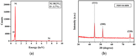
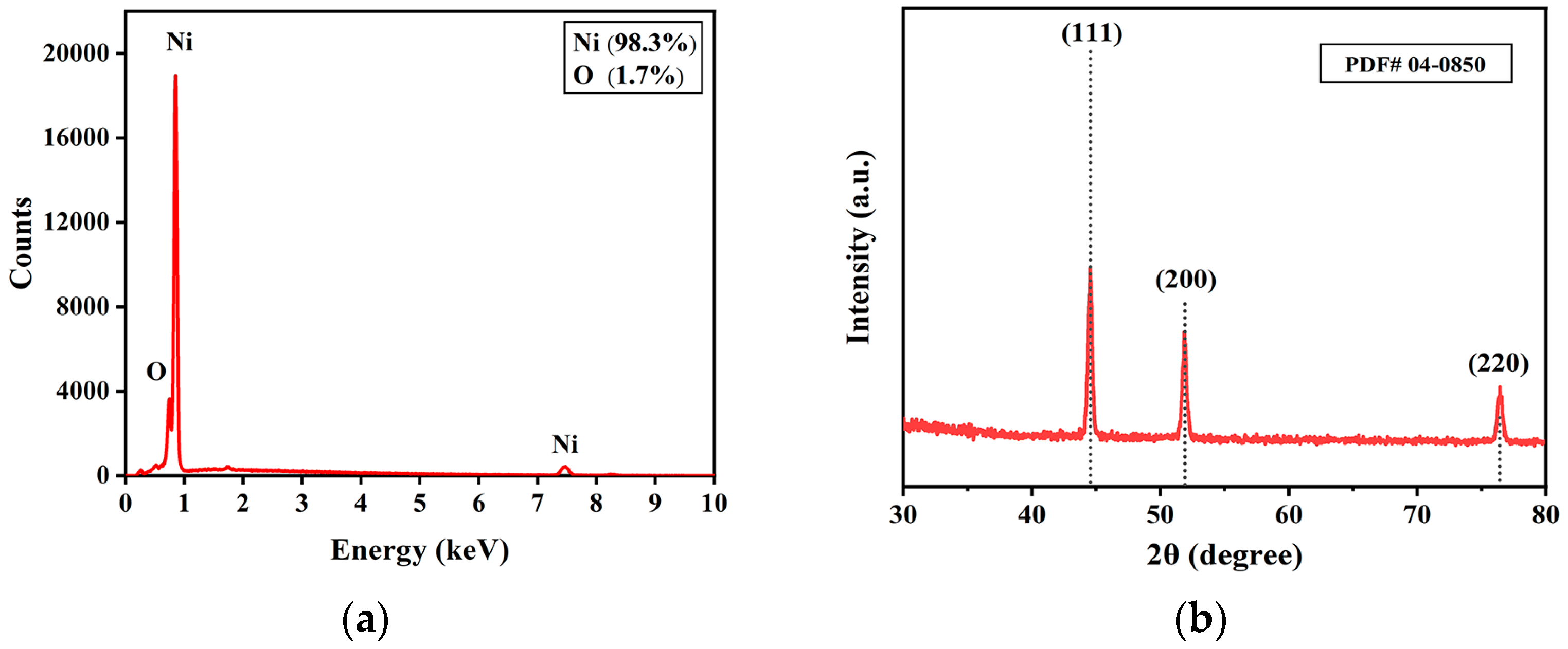
Figure 1a is the EDS result of the H2-sputtered Ni film on Si substrate, showing that the film contains mainly the Ni atoms (98.3%) with O as the only impurity, showing high purity of Ni film prepared under the processing parameters. After analysis by Jade software (MDI Jade 6.5), it was found that the GIXRD patterns of the films (Figure 1b) have only Ni peaks at 44.5°, 51.8°, and 76.3°, attributed to (111), (200), and (220) crystal planes, respectively. The crystalline grain size of the Ni films calculated with Scherrer’s formula is ~30 nm, manifesting that the films are composed of nano crystalline grains and O impurity did not affect the crystalline structure much.
Figure 1.
(a) EDS result and (b) GIXRD pattern for the Ni thick film sputtered under 250 W, 150 °C, 0.3 Pa and 3.5 sccm/25 sccm (H2/Ar).
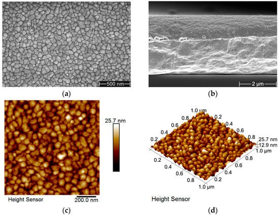
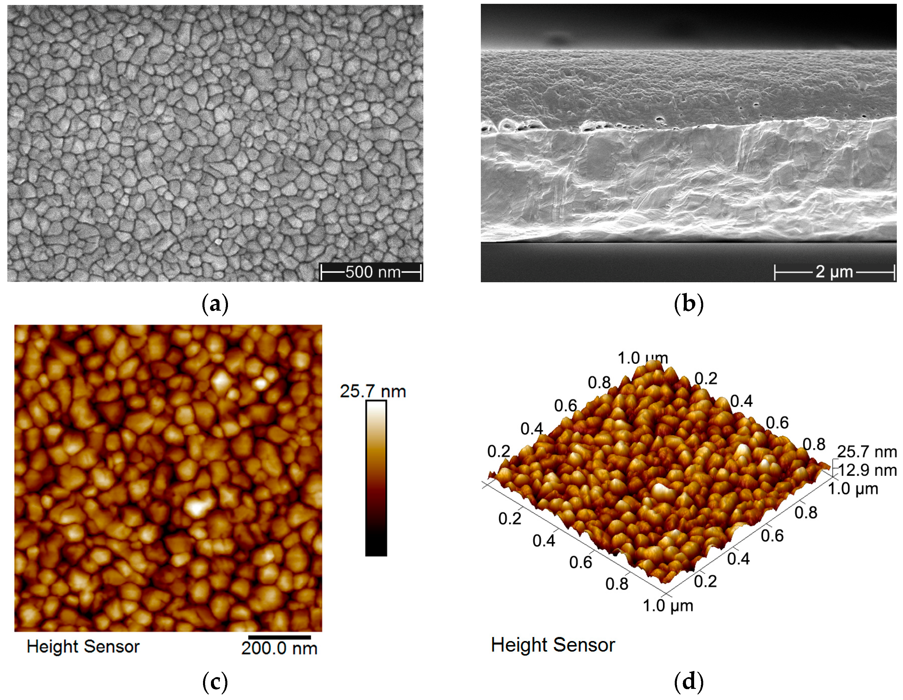
Figure 2 shows the microscopic structure and morphology of the H2-sputtered Ni thick film. It can be seen from Figure 2a that the surface is of a smooth and fine-grained morphology, and Figure 2b demonstrates a dense and uniform structure of the cross-section, without any columnar or porous structure observed, which indicates that these optimized sputtering parameters enhanced deposition rate without compromising structural integrity. Figure 2c,d provide two-dimensional and three-dimensional AFM surface images of the Ni film, which is consistent with the SEM results, and highlight a low surface roughness of 2.71 nm, corresponding to a larger grain formed during the thick film growth while maintaining good film density.
Figure 2.
Pictures for the microscopic structure and morphology of the Ni thick film sputtered under 250 W, 150 °C, 0.3 Pa and 3.5 sccm/25 sccm (H2/Ar). (a,b) SEM surface and cross-sectional pictures, (c,d) 2D and 3D AFM surface pictures.
3.2. Morphology of the Ni Thick Films on Polished Ti Substrates
Due to the high-purity Ni thick films achieved on Si substrate at a high deposition rate and with a smooth surface and compact cross-sectional morphology, Ni films with larger thickness (5.4 µm and 10.8 µm) were sputtered on polished Ti substrates under the same optimized parameters at a deposition rate of 45 nm/min, as on the Si substrates, for the adhesion test with friction and scratch methods.
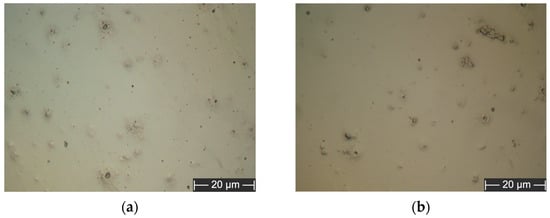
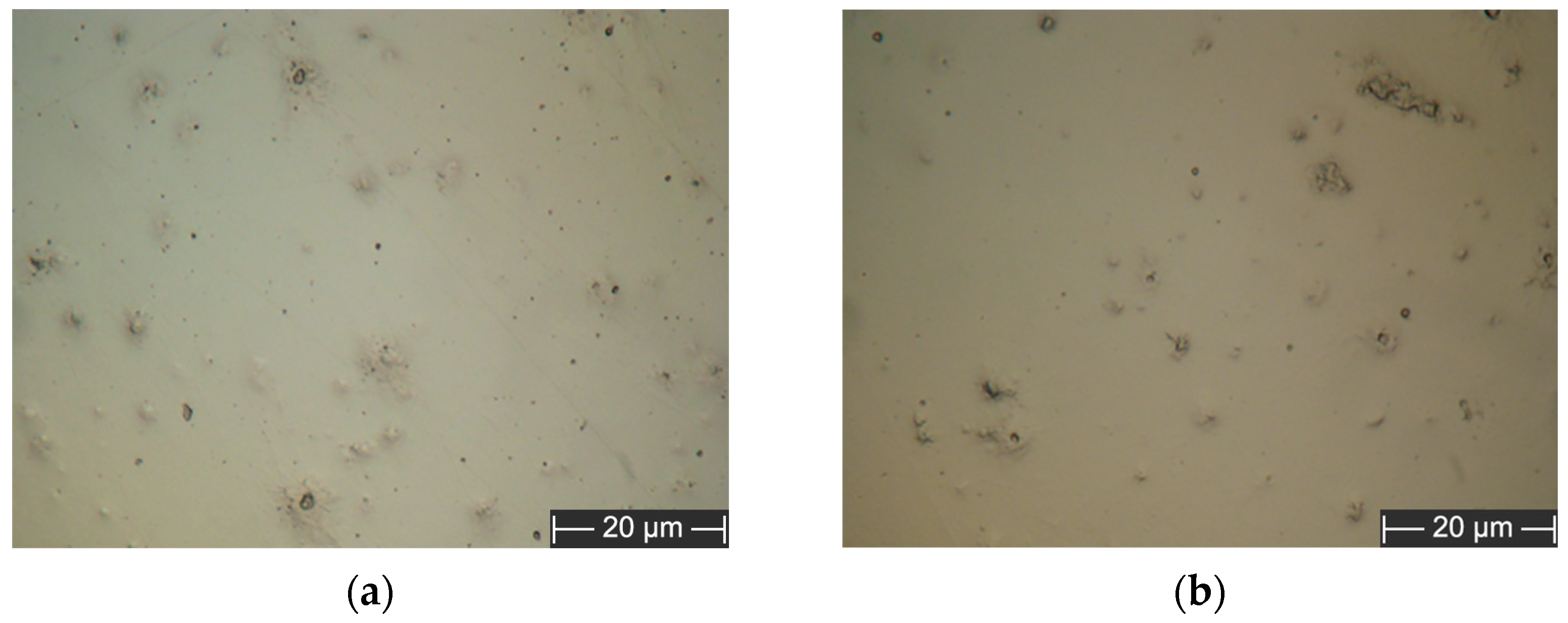
Optical micrographs provide insights into the progression of surface morphology from polished Ti substrate to Ni thick films of 5.4 µm and 10.8 µm thickness. The polished Ti substrate (Figure S1) shows visible irregularities, including dark spots and scratches, attributed to residual polishing imperfections. For the 5.4 µm thick Ni film (Figure 3a) sputtered over 120 min, surface coverage improves significantly, yet small pinholes and dark spots persist due to incomplete coalescence of Ni atoms in the early deposition stages. For the 10.8 µm thick Ni film (Figure 3b) after 240 min of sputtering, the surface exhibits greater uniformity as additional Ni atoms fill voids and pinholes, forming a dense, continuous layer with fewer imperfections. This progression demonstrates the critical role of the deposition time and the films’ thickness in achieving smoother and defect-free films.
Figure 3.
Optical micrographs of (a) 5.4 μm thick and (b) 10.8 μm thick Ni films on the polished Ti substrates.
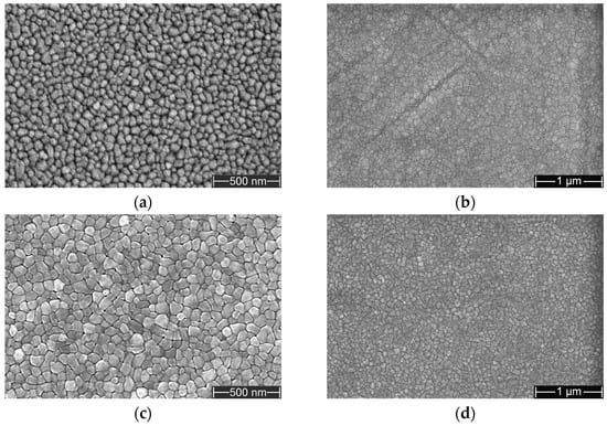
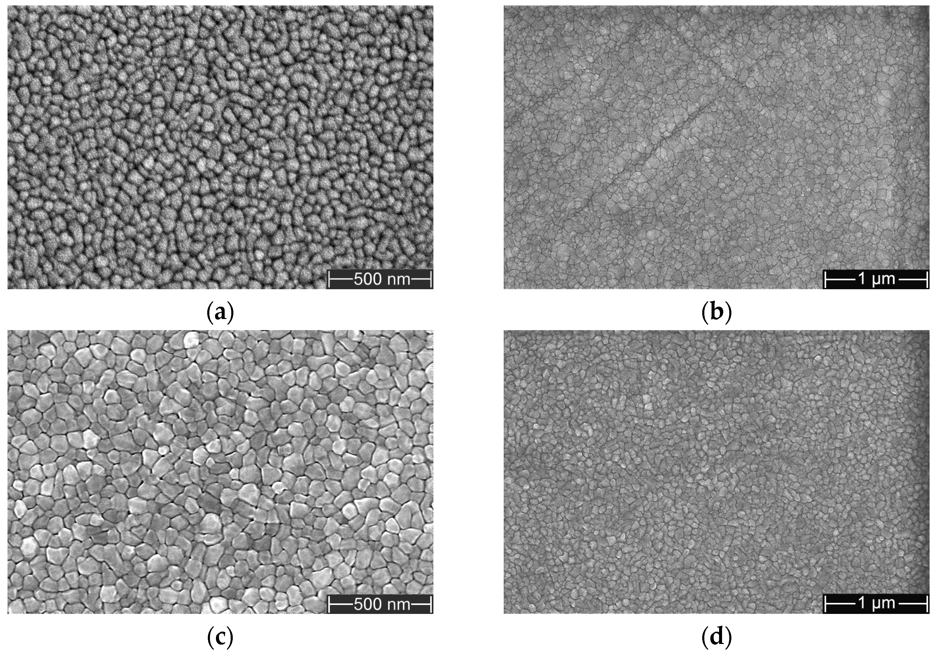
SEM images of polished Ti substrate under different magnifications (Figure S2) display typical mechanical polishing defects, including micro-scratches and pits. For the 5.4 µm Ni thick film, the surface (Figure 4a,b) shows a granular structure with visible grain boundaries at high magnification, indicating compact but slightly irregular grains. The low-magnification image shows a smoother and more continuous Ni layer than the uncovered Ti surface, reflecting a good initial coverage. However, there are still visible scratches on the surface due to the Ti substrate’s effect. The 10.8 µm thick film under different magnifications (Figure 4c,d) exhibits more refined large-size grains but still more compact and with better uniformity. The surface does not show effects of substrate surface, that ensure the high integrity of the Ni thick film. It is evident from a comparison between Figure 4a and c that a larger film thickness promotes grain growth in the Ni films.
Figure 4.
SEM surface morphology of (a,b) 5.4 µm thick and (c,d) 10.8 µm thick Ni films on the polished Ti substrate under different magnifications of (a,c) 100,000× and (b,d) 50,000×.
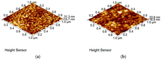
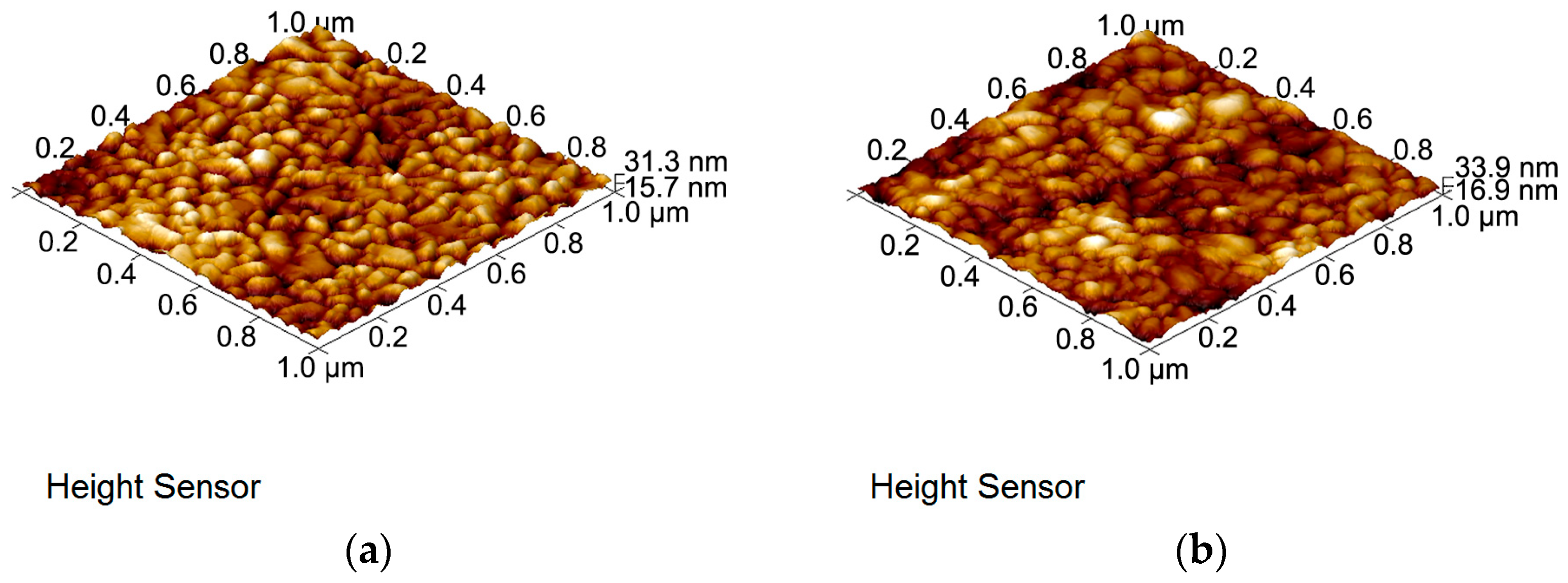
AFM analysis (Figure S3 and Figure 5) highlights the evolution of the surface roughness from the polished Ti substrate to Ni films of increasing thickness. The Ti substrate (Figure S3) exhibits a relatively rough surface (Ra = 4.44 nm) with visible linear scratches. For the 5.4 µm Ni film (Figure 5a), the roughness decreases to Ra = 3.68 nm, with a granular structure. The 10.8 µm film (Figure 5b) maintains a similar roughness (Ra = 3.70 nm) but displays a more compact and interconnected grain structure, reflecting improved compactness and uniformity. The minimal roughness change between the two films suggests that the additional deposition time enhances grain growth without introducing significant surface irregularities.
Figure 5.
AFM surface images of (a) 5.4 μm thick and (b) 10.8 μm thick Ni films on the polished Ti substrates.
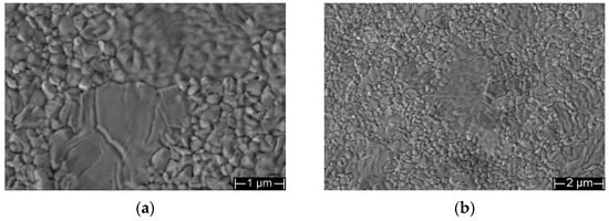
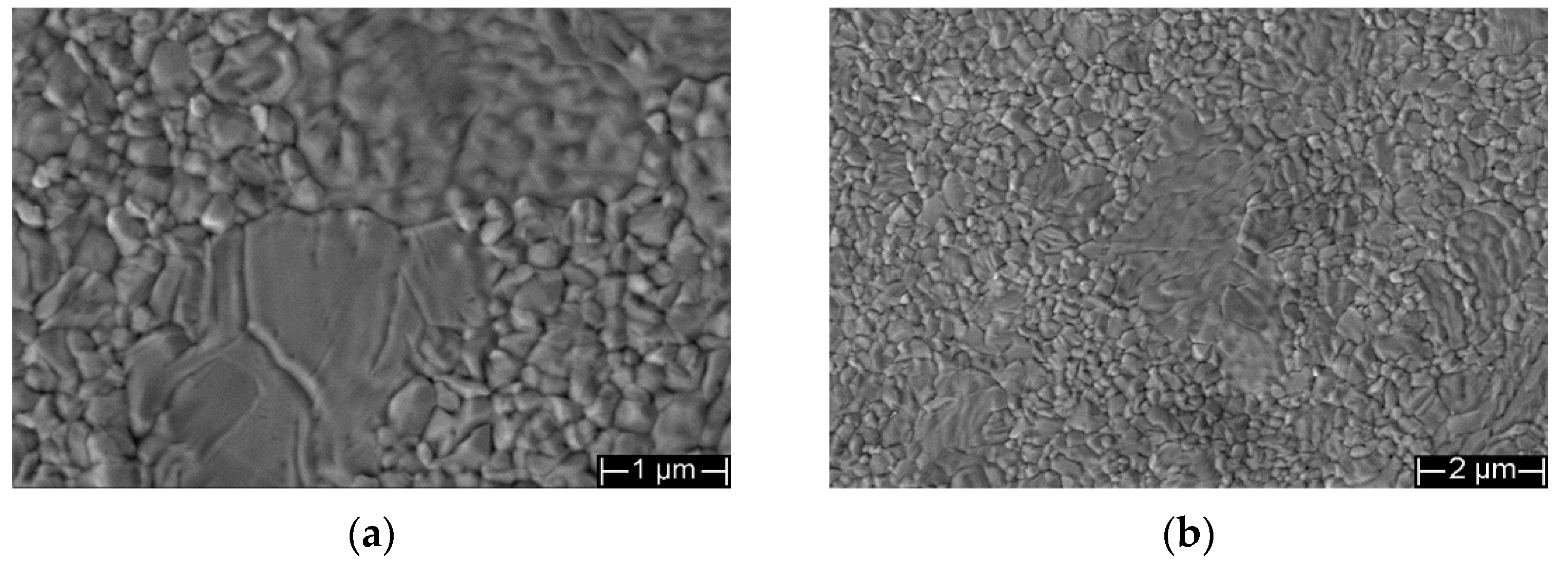
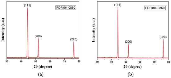
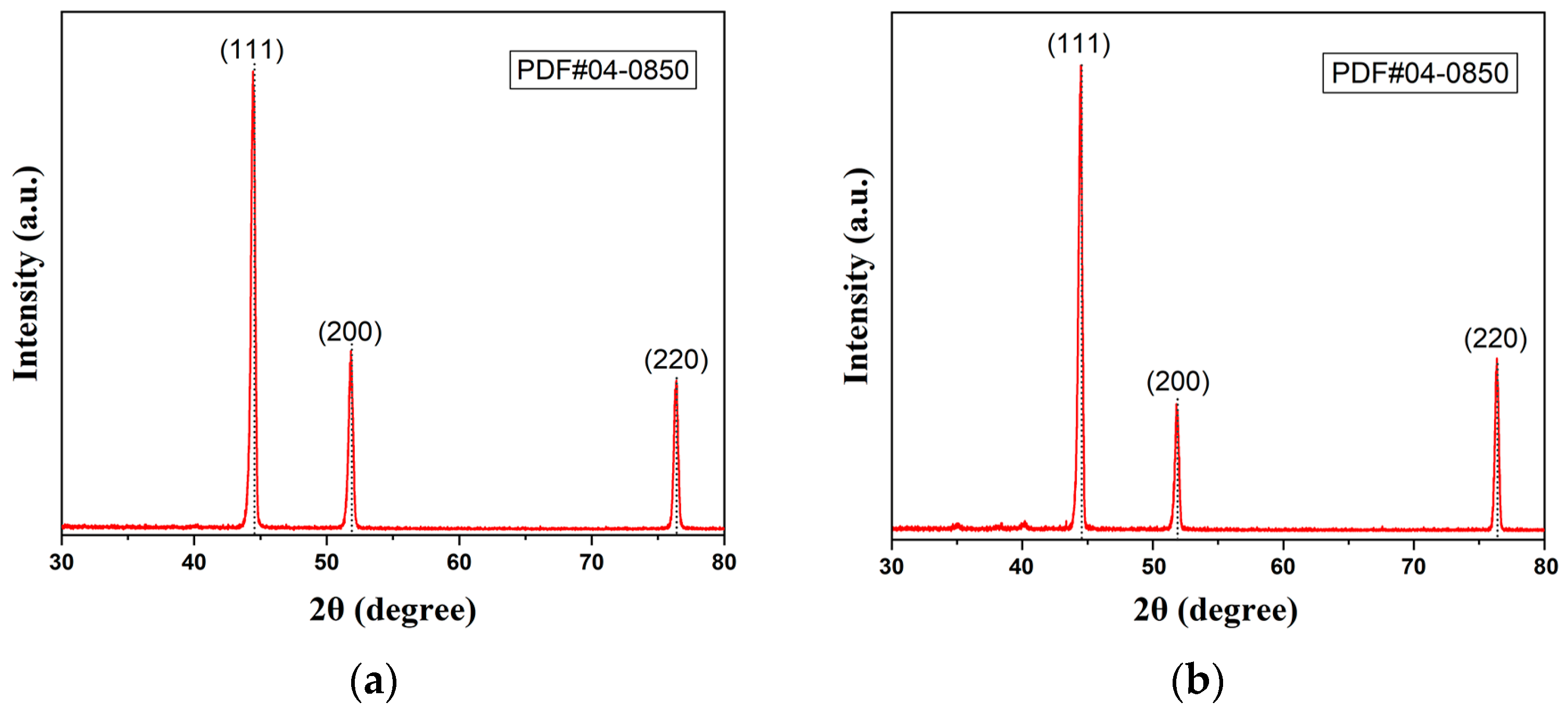
The Ni thick films on Ti substrates were further subjected to annealing to enhance their compactness and adhesion strength with the substrates, since the internal stress of thin films usually increases with film thickness and hence deteriorates their adhesion strength. Figure 6 shows the surface SEM images for the 5.4 μm thick post-annealed Ni film on Ti substrate. Apparent grain growth can be seen in the annealed film by comparing Figure 6a and Figure 4a. It is noticeable that significant grain coalescence occurred, which resulted in abnormal grain growth in the Ni thick film. However, the post-annealed Ni film still maintained a smooth surface and a more compact microstructure than the pre-annealed counterpart. GIXRD results (Figure 7) indicate that the grain size increased from ~22 nm for the pre-annealed Ni film to ~46 nm for the post-annealed sample. By comparing Figure 1b with Figure 7a and Figure 2a with Figure 4a, respectively, it can be concluded that the Si substrate promoted the grain growth in the Ni films.
Figure 6.
SEM surface morphology of the 5.4 μm thick post-annealed Ni film on Ti substrate under different magnifications of (a) 20,000× and (b) 10,000×.
Figure 7.
GIXRD patterns for the (a) pre-annealed and (b) post-annealed 5.4 μm thick Ni films.
3.3. Tribological Properties of the Ni Thick Films on Polished Ti Substrates
The adhesion strength of the Ni thick films to Ti substrates was first qualitatively evaluated using friction tests following the Burnish method in standard B571. The present investigation also concentrated on the comparative coefficient of friction (COF) and wear-scar morphology of the films, without considering quantitative wear parameters such as wear rate or wear volume. To avoid premature failure and substrate effects, based on the load-bearing capacity of each film thickness, different load ranges and test times were selected attentionally. Samples before annealing: the 5.4 µm thick films were tested at 1 Hz frequency, under 1 N load, and for 1 min and 5 min; the 10.8 µm thick films were tested at 1 Hz frequency, under 3 N and 5 N loads, and for 5 min. Samples after annealing at 400 °C for 5 h: both the 5.4 µm and the 10.8 µm thick films were tested at 1 Hz frequency, 3 N, 5 N and 7 N loads, and for 5 min.
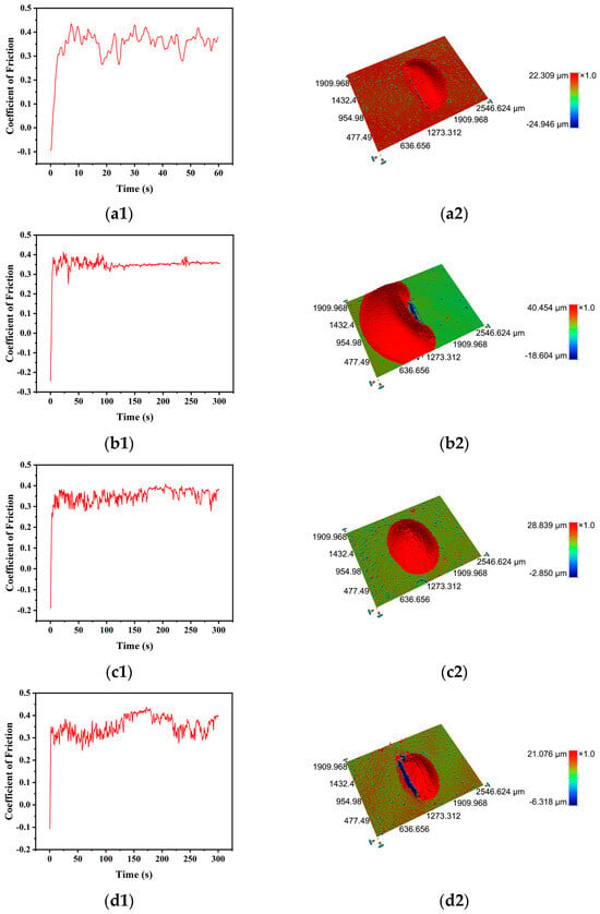
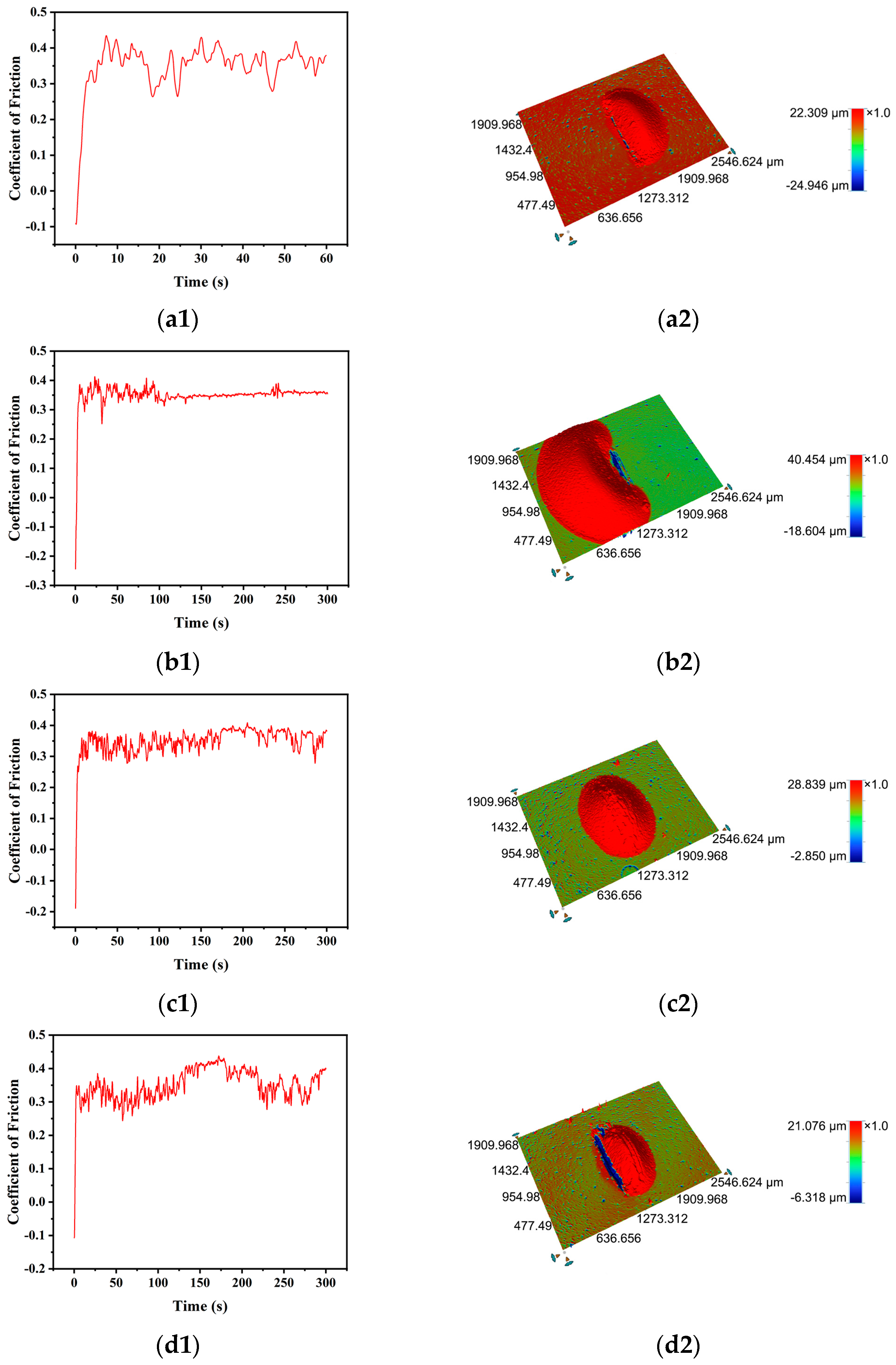
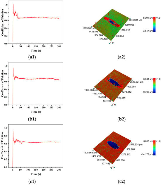
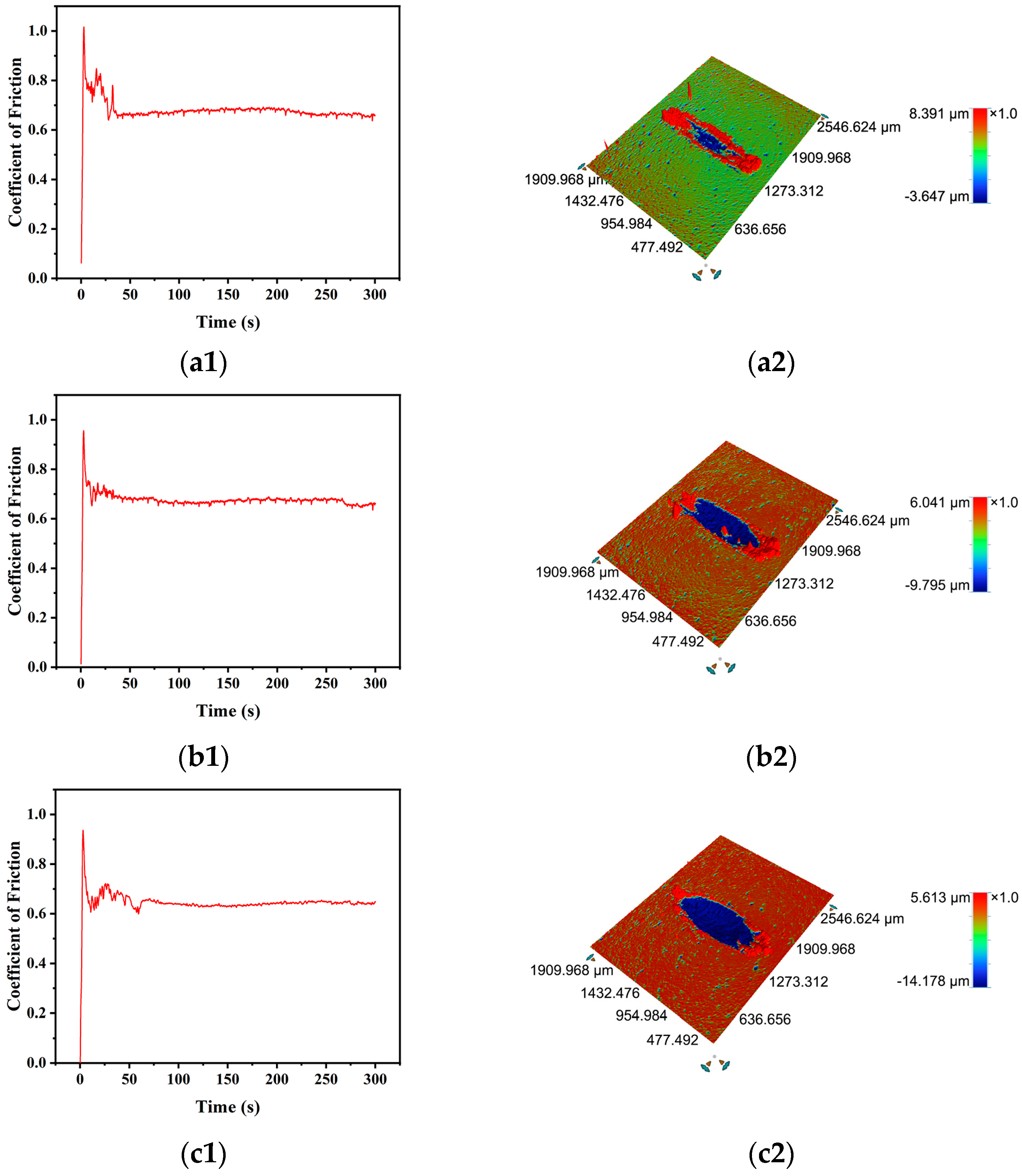
As shown in Figure 8(a1,b1), the as-sputtered, 5.4 µm thick Ni films showed uncertainty in COF with variations ranging from 0.3 to 0.45 within the first 100 s, and then came to a relatively stable value around 0.35, indicating a running-in period of ~100 s. Figure 8(a2,b2) illustrate raised scars with heights of 22.31 µm and 40.45 µm, respectively, for 5.4 µm thick as-sputtered Ni films under 1 N load for 1 min and 5 min friction tests. The smooth and integrated surface morphologies of the raised scars suggest the occurrence of local peeling-off of the films from the substrates. It can be clearly seen that the height and width of the peeling-off area are enlarged with prolonging the test time. The as-sputtered, 5.4 µm thick Ni film was also subjected to a conventional polishing process with 5% ZrO2 (average particle size of 1 µm) suspension, under a 0.01 MPa load at 60 rpm. The film peeled off from the substrate completely after being polished for 5 min (Figure S4a), which was consistent with the peeling-off behavior observed in the friction test.
Figure 8.
Friction test results for the as-deposited (a1,a2,b1,b2) 5.4 µm thick and (c1,c2,d1,d2) 10.8 µm thick Ni films on the polished Ti substrates. (a1–d1) COF curves, (a2–d2) 3D surface profiles of the wear scars. The 5.4 µm thick Ni films are tested at 1 Hz, under 1 N and for (a1,a2) 1 min and (b1,b2) 5 min, respectively. The 10.8 µm thick Ni films are tested at 1 Hz, for 5 min and under (c1,c2) 3 N and (d1,d2) 5 N, respectively.
As shown in Figure 8(c1,d1), the as-sputtered, 10.8 µm thick Ni film under higher loads (3 N and 5 N) exhibited the similar instability in COF as that for the 5.4 µm thick ones, and the oscillation lasted throughout the whole test time of 5 min, meaning a longer running-in period than the 5.4 µm thick Ni films. The corresponding raised scars shown in Figure 8(c2,d2) for the as-sputtered, 10.8 µm thick Ni films after the friction test shrank in both height and width in comparison with the scar in Figure 8(b2), indicating a less severe peeling-off of the 10.8 µm thick Ni films from the Ti substrates. This implies stronger adhesion of the 10.8 µm thick Ni film to the Ti substrate than that of the 5.4 µm thick Ni film. This was also verified by the polishing result of the 10.8 µm thick Ni film (polished under the same parameters as the as-sputtered, 5.4 µm thick Ni film), as shown in Figure S4b. For both thicknesses of Ni films, only small erosion craters appear at the edges of the peeling-off regions, and no erosion crater even occurs in Figure 8(c2), indicating that the surface abrasion of the as-sputtered Ni thick films is rather weak.
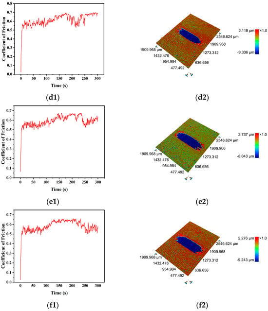
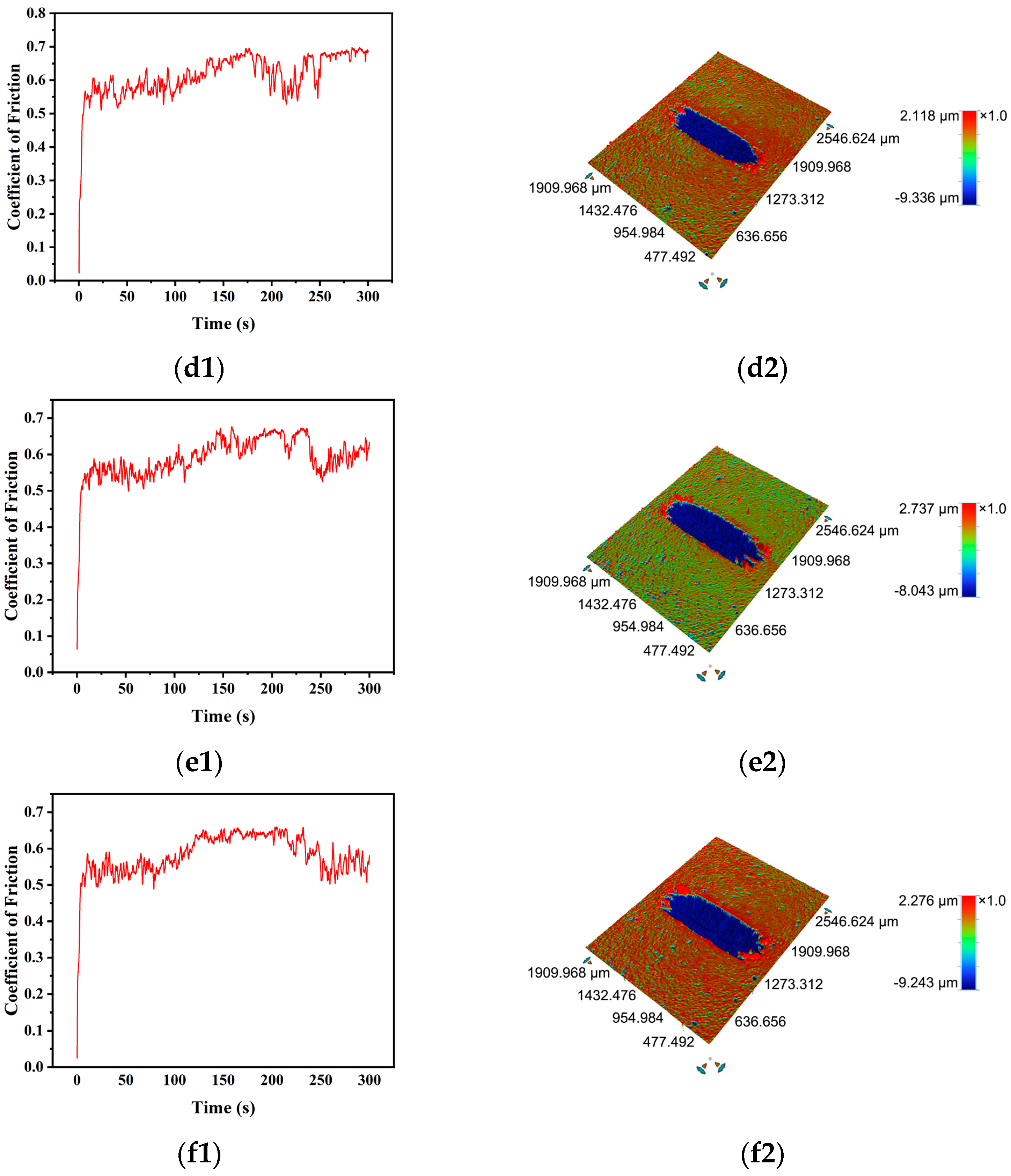
Figure 9 shows the COF and 3D surface profiles of the wear scars for the post-annealed Ni thick films. For the 5.4 µm thick, post-annealed Ni films, all the COF curves under different loads are similar, first oscillating within the running-in period and finally coming to a stable value. The corresponding wear scars are erosion craters with raised, cracked, and rough edges, which arise from the pile-up of the film during the friction process. It is obvious that the erosion crater deepens and the rough edge diminishes with increasing the load. After polishing the 5.4 µm thick, post-annealed Ni film (polished under the same parameters as the as-sputtered, 5.4 µm thick Ni film), an integrated film with a very smooth surface was found to adhere tightly to the Ti substrate, as shown in Figure S4c, indicating a very strong adhesion strength of the post-annealed Ni film. For the 10.8 µm thick, post-annealed Ni films, all the COF curves under different loads oscillate throughout the test time and have a rising trend with time, which are very different from those for the post-annealed 5.4 µm thick films, but the erosion craters are similar to those for the 5.4 µm thick, post-annealed films, except for the very weak pile-up edges. These phenomena show that the 10.8 µm thick films suffered severe wear, but the depth of the craters for the 5.4 µm thick, post-annealed films is close to or larger than the films’ thickness, and the depth of the craters for the 10.8 µm thick, post-annealed films is smaller than the films’ thickness, manifesting the importance of increasing the film’s thickness. The polishing result of the 10.8 µm thick, post-annealed Ni film (polished under the same parameters as the as-sputtered, 5.4 µm thick Ni film) is the same as the 5.4 µm thick, post-annealed Ni film.
Figure 9.
Friction test results for the post-annealed (a1–c2) 5.4 µm thick and (d1–f2) 10.8 µm thick Ni films on the polished Ti substrates. (a1–f1) COF curves, (a2–f2) 3D surface profiles of the wear scars. All the Ni thick films were tested at 1 Hz, for 5 min and under (a1,a2,d1,d2) 3 N, (b1,b2,e1,e2) 5 N, (c1,c2,f1,f2) 7 N, respectively.
3.4. Scratch Results of the Ni Thick Films on Polished Ti Substrates
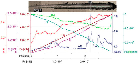
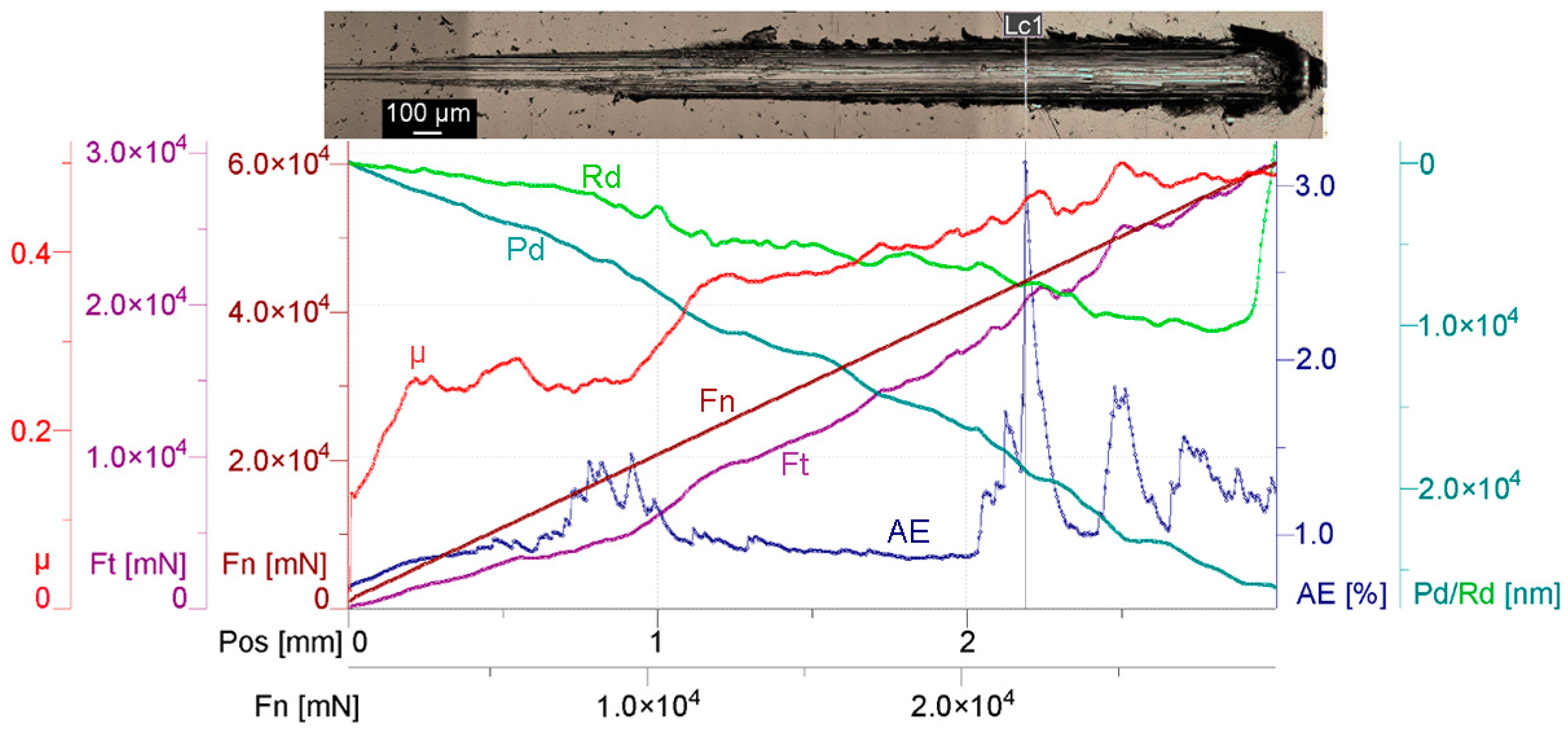
In order to qualitatively evaluate the adhesion strength of the Ni thick films to the Ti substrates, high-load scratch tests were conducted. Figure 10 shows the scratch test results for the 5.4 µm thick, post-annealed Ni film, with multiple signals acquired to characterize the scratch process. It can be clearly seen that the scratch depth Pd increases nearly linearly as the load Fn increases from 1 N to 60 N, reaching a maximum value of more than 25 µm, which is much larger than the film’s thickness. However, the residual depth Rd is much smaller than Pd, indicating a significant elastic/plastic recovery. Many intense acoustic emissions (AE) occurred during the scratch process, indicating multiple types of surface damage. The first emission was detected over the position (Pos) range of 0.69–1 mm under loads of 14,728–210,542 mN. The second emission appeared over 2.03–2.32 mm under loads of 41,082–46,669 mN. Immediately afterwards, numerous additional acoustic emissions were observed. Accordingly, the COF µ and the frictional force Ft varied.
Figure 10.
Scratch results for the 5.4 µm thick, post-annealed Ni film. The scratch direction is from left to right.
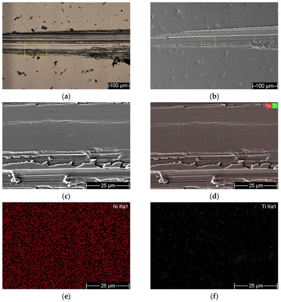
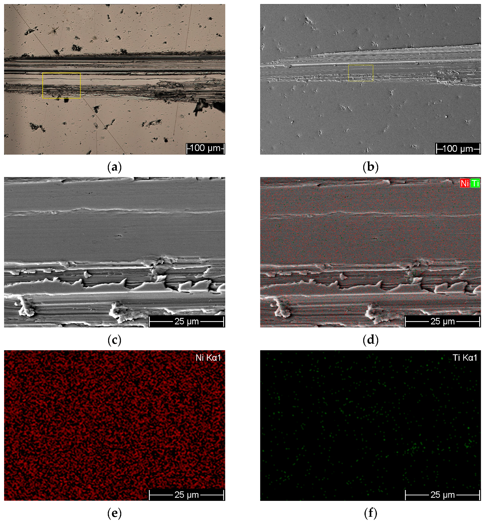
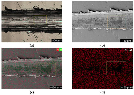
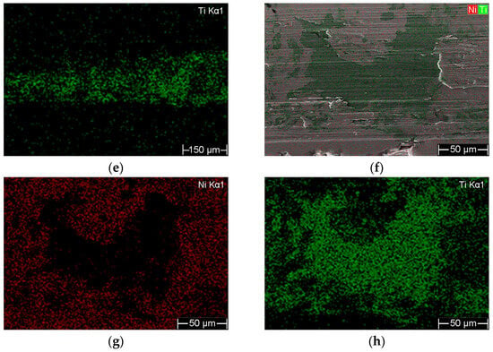
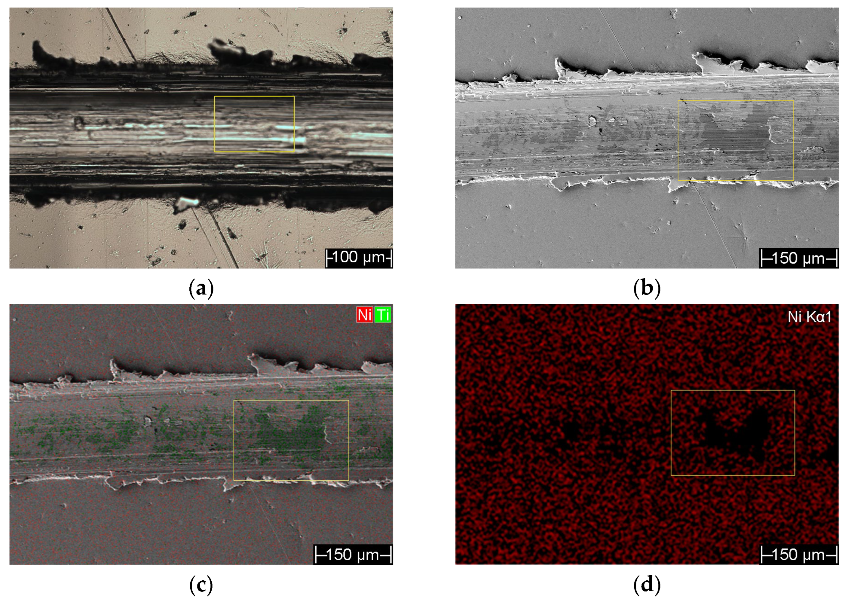
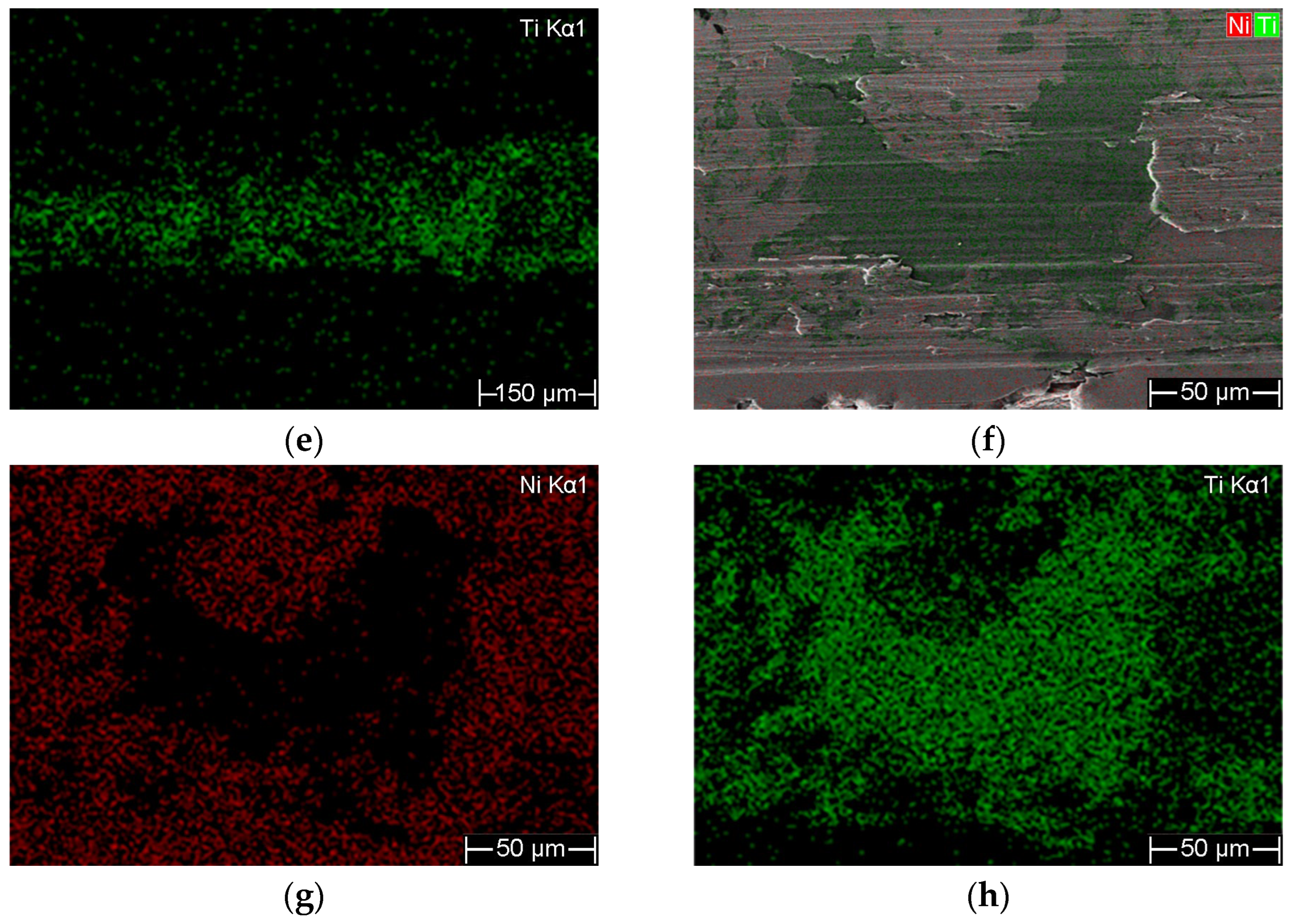
SEM and EDS elemental mapping were employed to analyze the scratch track, and the results are presented in Figure 11 and Figure 12. The results shown in Figure 11 reveal that, during the early stage of scratching, only the film surface was damaged, and severe damage occurred, causing the first acoustic emission. EDS results confirm that the Ti substrate is still completely covered by the Ni film. So, cohesive failure occurred to the film in this stage. The results in Figure 11 reveal that the Ni film is cracked and peeled off from the Ti substrate, leading to the second acoustic emission. The exposed Ti region appears darker gray than the Ni film surface. So, the film underwent adhesive failures in this stage. At the end of the scratch, the peeling-off area expanded (Figure S5), which caused more acoustic emissions. According to the scratch analysis, it can be concluded that cohesive failure occurs to the post-annealed Ni film prior to adhesive failure. By comprehensively analyzing the SEM and AE results, the critical load Lc1 was finally determined, and by averaging the critical load values from three scratching, Lc1 for the 5.4 µm thick, post-annealed Ni film is 40,305 mN.
Figure 11.
SEM and EDS analysis of the scratch track at the position corresponding to the first acoustic emission (right before the position of 1 mm) in Figure 10. (a) The locally magnified optical image, (b) the corresponding SEM image, (c) the magnified SEM image of the area marked by the yellow frame in (a,b), (d–f) the EDS elemental mappings corresponding to (c).
Figure 12.
SEM and EDS analysis of the scratch track at the position corresponding to the second acoustic emission (right after the position of 2 mm) in Figure 10. (a) The locally magnified optical image, (b) the corresponding SEM image, (c–e) the EDS elemental mappings corresponding to (b), (f–h) the EDS elemental mappings of the area marked by the yellow frame in (b–d).
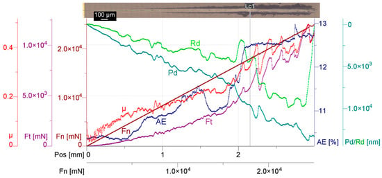
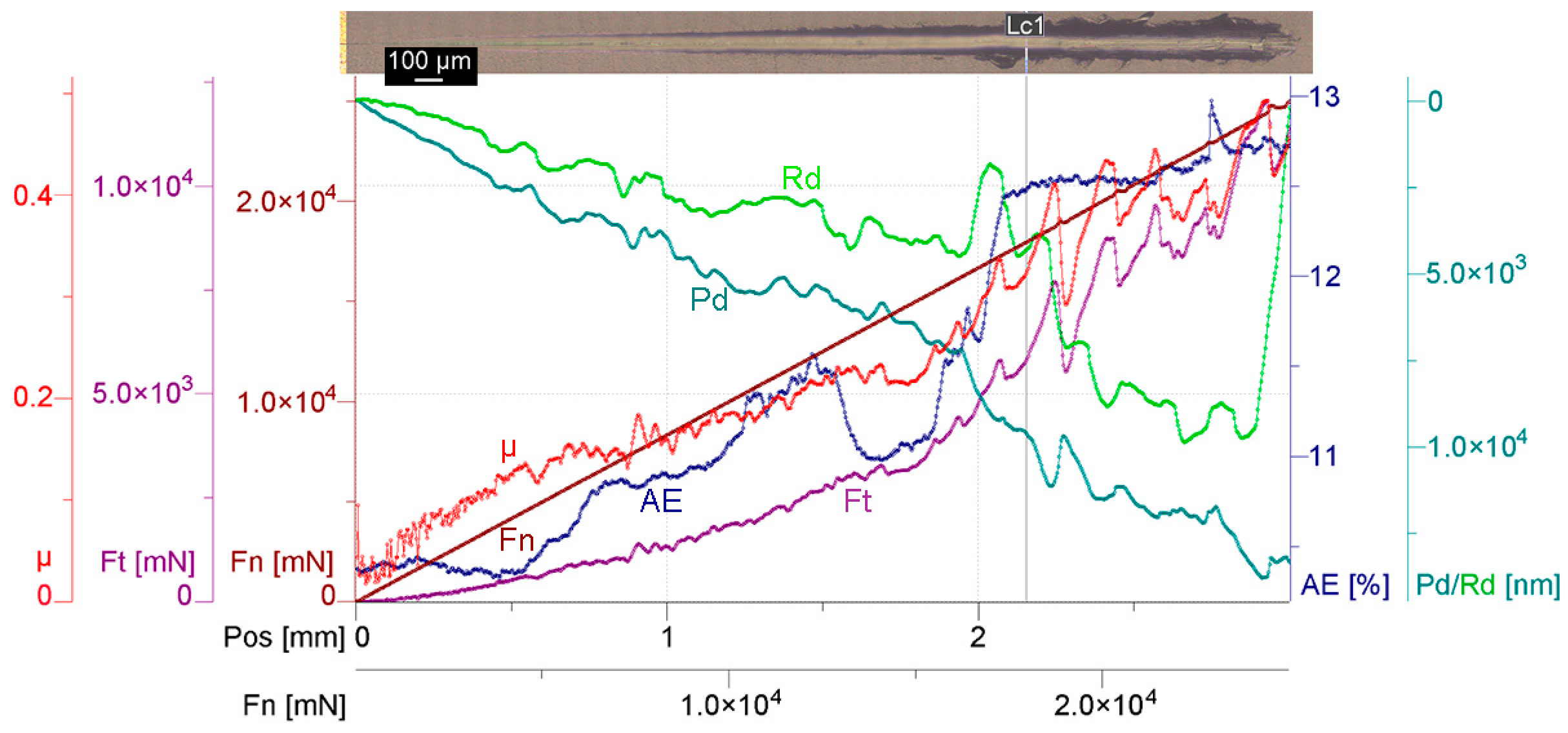
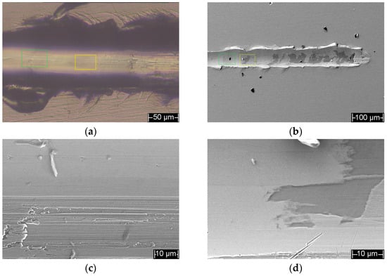
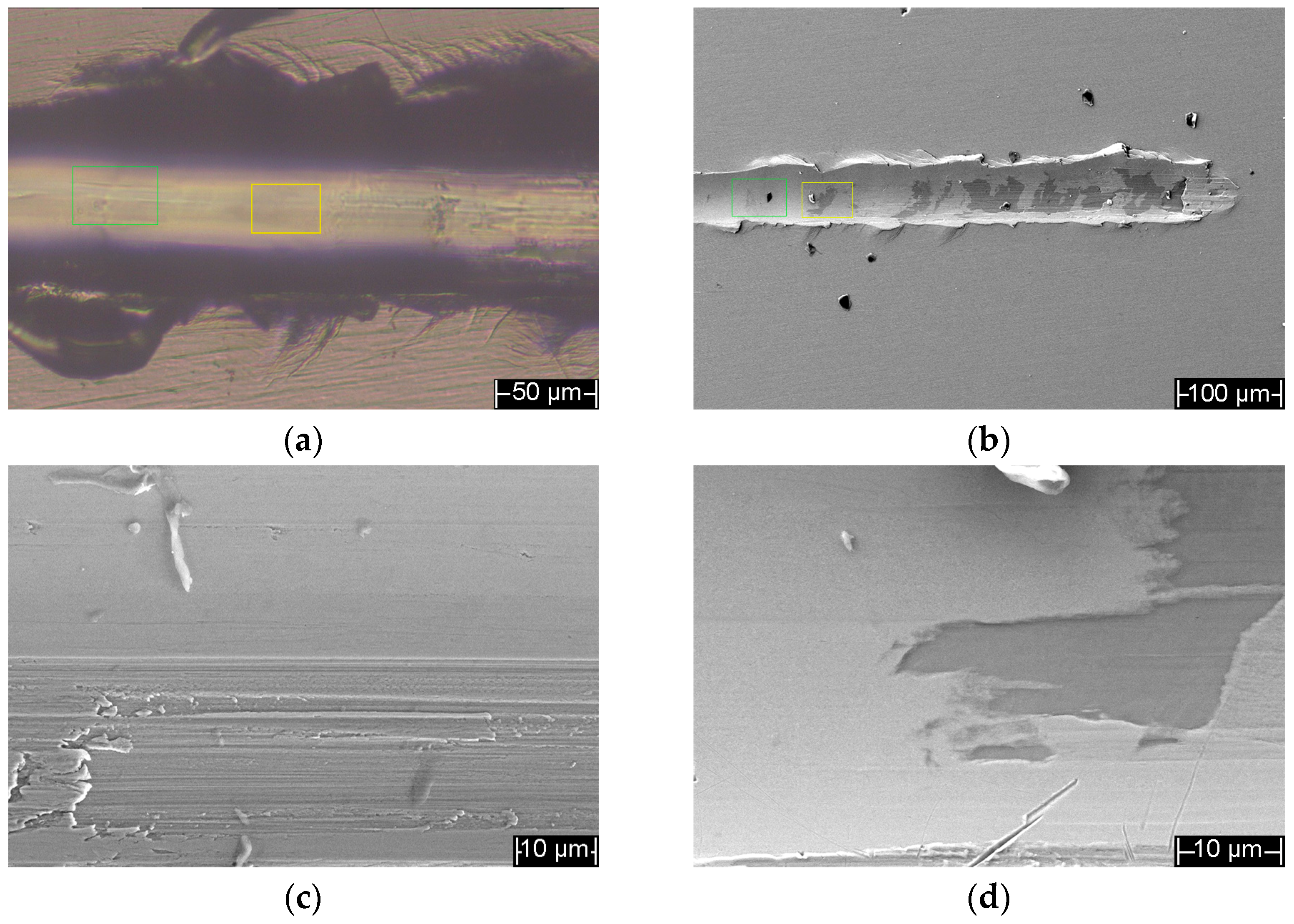
For comparison, the pre-annealed Ni film with a thickness of 5.4 µm was subjected to a scratch test, and the results are presented in Figure 13 and Figure 14. Considering the lower adhesion strength of the pre-annealed Ni film, a lower load range of 30–25,000 mN was selected. The pre-annealed film has similar scratch behavior to the post-annealed sample. A cohesive failure can be observed in Figure 14c, which is at the position of about 2 mm, under a load of ~17,422 mN. But the fractures are much weaker than those for the post-annealed films. Figure 14d reals an abrupt peeling-off of the pre-annealed Ni film, with no obvious cohesive failure zone nearby. The critical load of the pre-annealed film is ~18,263 mN, which is much lower than that of the post-annealed Ni film. It can be clearly seen from Figure 14b that, at the end of the scratch, large-area sections of the film were peeled off. Therefore, it can be concluded that the pre-annealed film is more prone to adhesive failure.
Figure 13.
Scratch results for the 5.4 µm thick, pre-annealed Ni film. The scratch direction is from left to right.
Figure 14.
Optical and SEM images of the scratch track in Figure 13. (a) Locally magnified optical image at the position around 2 mm, (b) SEM image of the scratch track, where the areas marked by the green and yellow frames are identical to those in (a), respectively, (c) the locally magnified SEM image of the green-framed region in (a,b), (d) the locally magnified SEM image of the yellow-framed region in (a,b), corresponding to Lc1.
As for the 10.8 µm thick films, a maximum load of 100 N was applied, but no useful information, especially no effective AE signal can be acquired, except for the SEM and EDS results. The SEM image (Figure S6) discovered weak peeling-off of very small sections of the post-annealed Ni film from the Ti substrate at the end of the scratch, under a load of ~94,843 mN, indicating a very high critical load for the film.
4. Discussion
The O impurity was mainly derived from the residual or leaked air inside the vacuum chamber during the sputtering process. The low O atomic content of the H2-sputtered Ni films was due to the chemical reductive reaction between H2 and O2: 2H2 + O2 = 2H2O↑, and the reaction product of water vapors can then be pumped out of the chamber by the vacuum system, therefore effectively reducing the oxygen content of the sputtered Ni film. Moreover, the addition of H2 enhances adatom mobility and suppresses oxide-related defects, promoting surface diffusion and film densification, as widely reported for sputtered metallic coatings [35,36,37], which contributes to the formation of compact structure of the Ni thick films without porous structures. Moreover, the surface defect sites will be easily filled by the adsorbent Ni atoms due to their large diffusion mobility and hence improve the surface integrity.
For all the as-sputtered Ni thick films, the COF level did not change much, but the running-in period changed with load. Linking the COF curves with the corresponding 3D surface profiles of the wear scars, it is obvious that the COF is not only related to the wear process of the films’ surface, but also reflects the local peeling-off process of the films, which was further verified the polishing process and scratch tests. The oscillation in the COF curves is mainly caused by the peeling-off process, since the raised scars due to the peeling-off are so significant and the erosion craters due to the surface wear are small. Observing the results for the 5.4 µm thick films in Figure 8(a1,a2,b1,b2), the interfacial damage even occurs at the beginning of the friction test, then expands quickly with test time, and finally stops expanding, which corresponds to the running-in process. The COF curve in Figure 8(a1) oscillates throughout the test time of 60 s just due to the test time being shorter than the running-in period (~100 s) that can be seen in Figure 8(b1), in which the oscillation in the COF stops after ~100 s and comes to a stable value of ~0.35, meaning the peeling-off region stops expanding at this point. Observing the results for the 10.8 µm thick films, the COF in Figure 8(c1) oscillates in a stable level between 0.3 and 0.4 throughout the test time, and only the humped scar occurs in Figure 8(c2), indicating that the oscillation is caused merely by the peeling-off process of the Ni thick film. The COF in Figure 8(d1) oscillates first in a low level between 0.3 and 0.4 and then in an elevated level above 0.4 during the test process, indicating that only the peeling-off occurs at first to cause the low-level oscillation, and then the erosion crater occurs to cause the high-level oscillation. The peeling-off of the 10.8 µm thick films is less severe than the 5.4 µm thick ones, although the former were subject to the friction test under higher loads and longer time than the latter; meanwhile, the running-in period for the former is much longer than that for the latter, demonstrating that thicker films have a much higher ability to block the stress caused by the friction to transfer to the interface between the Ni film and the Ti substrate and thus peels off at a low rate.
Both the 5.4 µm and the 10.8 µm thick Ni films after annealing have significant erosion craters as shown in Figure 9, instead of raised scars as the as-sputtered Ni thick films in Figure 8, indicating the post-annealed Ni thick films did not face peeling-off from the Ti substrate during the friction test process, and annealing of the films improved their adhesion strength, friction and wear performance effectively [28,29,38]. At the beginning of the friction test of the post-annealed Ni thick films, the surface underwent a scratching process, resulting in raised, cracked, and rough morphology and thus the oscillation in the COF, then material on the surface was removed in a short time and erosion crater occurred. For the 5.4 µm thick Ni films, once the erosion crater formed, its bottom became smooth with time, making the COF stop oscillation. For the 10.8 µm thick Ni films, the COF oscillated for all of the test time, perhaps due to the bottom of the erosion crater remaining rough all the way.
Recrystallization, grain growth, and interface diffusion between the film and the substrate as well occurred due to annealing at 400 °C for 5 h, and the surface became homogeneous with relieved internal stresses. These transformations promoted elastic recovery and enhanced the adhesion strength of the films. This is also supported by another study where they showed that the annealing has a significant relation between densification-driven recrystallization and diffusion-dominated interfacial modification. Through grain growth and defect annihilation, annealing primarily enhanced densification by high temperature in Ni films. In contrast, due to nanoscale interfaces and strong chemical affinity at elevated temperature, Ta-containing stacks activate Ni–Ta interdiffusion [39]. Comparatively to annealing, although thickness is less important, it played a secondary role due to blocking load transfer. Therefore, both as-sputtered and annealed 10.8 µm Ni thick films consistently outperformed the 5.4 µm Ni thick films. Annealing, however, reduced the performance gap, and allowed even the 5.4 µm Ni thick film to be feasible for high-load applications.
5. Conclusions
In this study, Ni thick films were deposited with RF magnetron sputtering in Ar atmosphere plus a small amount of H2. The Ni thick films were sputtered up to a thickness of 10.8 µm at a high deposition rate (45 nm/min) with high compactness, purity and a smooth surface, and additionally their strong adhesion strength was demonstrated through friction and scratch tests. Further research was extended to make a comparison between as-sputtered and post-annealed (400 °C for 5 h) Ni thick films. Post-annealed Ni thick films showed much better results compared to as-sputtered ones by promoting the adhesion strength of the films, and the latter featured more adhesive failure and the former more cohesive failure, indicated by both the wear scars after the friction tests and the scratch tracks. Annealing enabled the Ni thick films with thicknesses of 5.4 µm and 10.8 µm to achieve exceptional performance across the load range (3 N–7 N), while thicker films (10.8 µm) characteristically offered better load-bearing capacity. At higher loads, the 10.8 µm Ni thick film provided marginally superior consistency, which favors those applications that require strong adhesion, high compactness and durability under mechanical stress.
Supplementary Materials
The following supporting information can be downloaded at https://www.mdpi.com/article/10.3390/coatings16030279/s1, Figure S1: Optical micrographs of polished Ti substrate surface; Figure S2: SEM surface morphology of the polished Ti substrate under different magnifications of (a) 100,000×, (b) 50,000×, (c) 20,000×, and (d) 10,000×; Figure S3: AFM surface image of polished Ti substrate; Figure S4: Photographs of the Ni thick films on Ti substrates after polishing. (a) 5.4 µm thick, pre-annealed Ni film, (b) 10.8 µm thick, pre-annealed Ni film, and (c) 5.4 µm thick, post-annealed Ni film; Figure S5: SEM image for the ending area of the scratch track in Figure 10. The scratch is from left to right; Figure S6: SEM image for the ending area of the scratch track for the 10.8 µm thick, post-annealed film. The scratch is from left to right.
Author Contributions
Conceptualization, Y.L.; methodology, U.B.; formal analysis, U.B., Y.L., F.R. and H.W.; investigation, U.B., F.R., A.L., J.L., Y.M., H.W. and Y.Z.; resources, Y.L. and H.W.; data curation, Y.L. and U.B.; writing—original draft preparation, U.B.; writing—review and editing, Y.L.; supervision, Y.L.; project administration, Y.L.; funding acquisition, Y.L. All authors have read and agreed to the published version of the manuscript.
Funding
This research was funded by the project from the Science and Technology Bureau of Hanjiang District, Yangzhou City, Jiangsu Province.
Institutional Review Board Statement
Not applicable.
Informed Consent Statement
Not applicable.
Data Availability Statement
The corresponding author and the first author can provide with all the original data related to the paper on requests.
Acknowledgments
We would like to express our sincere gratitude to Anton Paar (Shanghai) Trading Co., Ltd. for their valuable support and assistance in the scratch test and corresponding analysis.
Conflicts of Interest
Author Yiwen Zhang was employed by the company Yangzhou Xiaguang Photoelectric Co., Ltd. The remaining authors declare that the research was conducted in the absence of any commercial or financial relationships that could be construed as a potential conflict of interest.
Abbreviations
The following abbreviations are used in this manuscript:
| RF | Radio frequency |
| sccm | Standard cubic centimeters per minute |
| GIXRD | Grazing incidence X-ray diffraction |
| FE-SEM | Field emission scanning electron microscope |
| EDS | Energy dispersive spectroscopy |
| AFM | Atomic force microscope |
| MFT | Multi-function tester |
| COF | Coefficient of friction |
| AE | Acoustic emission |
References
- Zhang, K.; Yuan, W.; Ma, H.; Wang, T.; He, Y.; Shi, X.; Wu, L. Effects of current on the microstructure and frictional behavior of Ni/CNTs films fabricated on Cu substrates. Ind. Lubr. Tribol. 2026. ahead-of-print. [Google Scholar] [CrossRef] [Scilit]
- Zhang, M.; Xu, F.; Lin, D.; Peng, J.; Zhu, Y.; Wang, H. A smart anti-corrosion coating based on triple functional fillers. Chem. Eng. J. 2022, 446, 137078. [Google Scholar] [CrossRef] [Scilit]
- Zeng, Q. Influence of CePO4 on high temperature anti-friction and anti-wear behaviors of nickel-based h-BN composite coatings. Diam. Relat. Mater. 2024, 148, 111421. [Google Scholar] [CrossRef] [Scilit]
- Chen, N.; Xu, X.; Liao, Y.; Deng, J.; Yu, J.; Zhang, Y.; Cai, Q.; Tang, C.; Li, Y. A robust, flexible, and high thermal conductivity superhydrophobic film prepared by thiol-ene photopolymerization for waterproofing and anti-corrosion. Polymer 2025, 336, 128892. [Google Scholar] [CrossRef] [Scilit]
- Zhang, L.; Wang, J.; Zhou, S.; Luo, X.; Li, Y. Rapid realization of ultra-high vacuum packaging of atomic chips by thick film technology. Vacuum 2023, 213, 112113. [Google Scholar] [CrossRef] [Scilit]
- Suk, K.L.; Choo, K.; Kim, S.J.; Kim, J.S.; Paik, K.W. Studies on various chip-on-film (COF) packages using ultra fine pitch two-metal layer flexible printed circuits (two-metal layer FPCs). Microelectron. Reliab. 2012, 52, 1182–1188. [Google Scholar] [CrossRef] [Scilit]
- Tao, S.; Yang, J.; Shao, F.; Zhao, H.; Zhong, X.; Zhuang, Y.; Sheng, J.; Ni, J.; Li, Q.; Tao, S. Atmospheric plasma sprayed thick thermal barrier coatings: Microstructure, thermal shock behaviors and failure mechanism. Eng. Fail. Anal. 2022, 131, 105819. [Google Scholar] [CrossRef] [Scilit]
- Huang, Z.; Zhou, W.; Tang, X.; Luo, F.; Zhu, D. High-temperature application of the low-emissivity Ni/Au films on alloys. Appl. Surf. Sci. 2010, 256, 6893–6898. [Google Scholar] [CrossRef] [Scilit]
- Singh, S.; Basu, S. Structure and morphology of the Ni films grown by different deposition methods. Surf. Coat. Technol. 2006, 201, 952–957. [Google Scholar] [CrossRef] [Scilit]
- Potočnik, J.; Novaković, M.; Perović, M.; Bošković, M.; Bundaleski, N.; Popović, M. Exploring thickness-dependent structural, chemical and magnetic properties of nanostructured nickel thin films. Vacuum 2024, 230, 113619. [Google Scholar] [CrossRef] [Scilit]
- Priyadarshini, B.G.; Aich, S.; Chakraborty, M. Structural and morphological investigations on DC-magnetron-sputtered nickel films deposited on Si (100). J. Mater. Sci. 2011, 46, 2860–2873. [Google Scholar] [CrossRef] [Scilit]
- Bhatti, J.; Fazal, M.A.; Faheem Khan, A.; Bushroa, A.R.; Quazi, M.M. Investigation of the mechanical properties of electrodeposited nickel and magnetron sputtered chromium nitride coatings deposited on mild steel substrate. J. Adhes. Sci. Technol. 2016, 30, 2224–2235. [Google Scholar] [CrossRef] [Scilit]
- Behera, A.; Aich, S.; Behera, A.; Sahu, A. Processing and characterization of magnetron sputtered Ni/Ti thin film and their annealing behaviour to induce shape memory effect. Mater. Today Proc. 2015, 2, 1183–1192. [Google Scholar] [CrossRef] [Scilit]
- Tiwari, S.K.; Rao, A.U.; Chawla, V.; Pant, G.; Verma, P.C.; Gunupuru, R.; Avasthi, D.K.; Pandey, J.K.; Chawla, A.K. Effect of Ni Enrichment on the Microstructure, Mechanical, and Tribological Properties of Hydrophobic Ni3Al Alloy Coatings. J. Mater. Eng. Perform. 2025, 34, 17256–17271. [Google Scholar] [CrossRef] [Scilit]
- Eadi, S.B.; Song, H.S.; Song, H.D.; Oh, J.; Lee, H.D. Nickel film deposition with varying RF power for the reduction of contact resistance in NiSi. Coatings 2019, 9, 349. [Google Scholar] [CrossRef] [Scilit]
- Koenig, T.R.; Rao, Z.; Chason, E.; Tucker, G.J.; Thompson, G.B. The microstructural and stress evolution in sputter deposited Ni thin films. Surf. Coat. Technol. 2021, 412, 126973. [Google Scholar] [CrossRef] [Scilit]
- Sharma, A.; Mohan, S.; Suwas, S. The influence of deposition temperature on the structure, microstructure, morphology and magnetic properties of sputter deposited nickel thin films. Thin Solid Film. 2016, 619, 91–101. [Google Scholar] [CrossRef] [Scilit]
- Geetha Priyadarshini, B.; Aich, S.; Chakraborty, M. On the microstructure and interfacial properties of sputtered nickel thin film on Si (1 0 0). Bull. Mater. Sci. 2014, 37, 1265–1273. [Google Scholar] [CrossRef] [Scilit]
- Yang, X.; Liu, S.; Wei, X.; Pan, B. Effects of annealing on the structure and microhardness of nanocrystalline Ni–Mn electrodeposits. J. Alloys Compd. 2023, 960, 170732. [Google Scholar] [CrossRef] [Scilit]
- Bhutta, M.U.; Khan, Z.A. Wear and friction performance evaluation of nickel based nanocomposite coatings under refrigerant lubrication. Tribol. Int. 2020, 148, 106312. [Google Scholar] [CrossRef] [Scilit]
- Zhang, X.; Ding, Y.; Ma, H.; Zhao, R.; Wang, L.; Zhang, F. Microstructure and Mechanical Properties of Co-Deposited Ti-Ni Films Prepared by Magnetron Sputtering. Coatings 2023, 13, 524. [Google Scholar] [CrossRef] [Scilit]
- Dzhumaliev, A.S.; Nikulin, Y.V.; Filimonov, Y.A. Formation of textured Ni (200) and Ni (111) films by magnetron sputtering. Tech. Phys. 2016, 61, 924–928. [Google Scholar] [CrossRef] [Scilit]
- Delvaux, A.; Lumbeeck, G.; Idrissi, H.; Proost, J. Effect of microstructure and internal stress on hydrogen absorption into Ni thin film electrodes during alkaline water electrolysis. Electrochim. Acta 2020, 340, 135970. [Google Scholar] [CrossRef] [Scilit]
- Muslim, N.; Soon, Y.W.; Lim, C.M.; Voo, N.Y. Properties of nickel films growth by radio frequency magnetron sputtering at elevated substrate temperatures. Thin Solid Film. 2016, 612, 82–86. [Google Scholar] [CrossRef] [Scilit]
- Hanya, Y.; Nakamura, R.; Okugawa, M.; Ishimaru, M.; Oohata, G.; Yasuda, H. Effects of hydrogen on structure and crystallization behavior of sputter-deposited amorphous germanium films. Jpn. J. Appl. Phys. 2020, 59, 075506. [Google Scholar] [CrossRef] [Scilit]
- Liu, X.; He, X.; Lin, Y.; Zhuang, J.; Hao, J. Enhanced adhesion strength and solid lubricity of graphite like amorphous carbon films by hydrogen implantation. Surf. Coat. Technol. 2021, 412, 127013. [Google Scholar] [CrossRef] [Scilit]
- Sun, Q.; He, J.; Nagao, A.; Ni, Y.; Wang, S. Hydrogen-prompted heterogeneous development of dislocation structure in Ni. Acta Mater. 2023, 246, 118660. [Google Scholar] [CrossRef] [Scilit]
- Du, Y.; Yang, X.; Nie, K.; Peng, Y.; Du, H.; Tang, Z. Effects of high annealing-temperature on the friction and corrosion behavior of magnetron sputtered CrAl coatings. Appl. Surf. Sci. 2025, 709, 163745. [Google Scholar] [CrossRef] [Scilit]
- Wan, Z.; Liu, C.; Gan, X. Microstructure and Tribological Properties of Ni@ CaF2/GH5188 Composites Fabricated from Nickel-Coated CaF2 Powder. Surf. Interfaces 2026, 83, 108553. [Google Scholar] [CrossRef] [Scilit]
- Dehm, G.; Medres, B.; Shepeleva, L.; Scheu, C.; Bamberger, M.; Mordike, B.L.; Mordike, S.; Ryk, G.; Halperin, G.; Etsion, I. Microstructure and tribological properties of Ni-based claddings on Cu substrates. Wear 1999, 225, 18–26. [Google Scholar] [CrossRef] [Scilit]
- Gyawali, G.; Joshi, B.; Tripathi, K.; Kim, S.H.; Wohn Lee, S. Effect of microtexturing on tribological performance of Ni/Ni–SiC composite coatings. Surf. Eng. 2015, 31, 701–707. [Google Scholar] [CrossRef] [Scilit]
- Zhang, H.; Li, D.Y. Effects of sputtering condition on tribological properties of tungsten coatings. Wear 2003, 255, 924–932. [Google Scholar] [CrossRef] [Scilit]
- Bull, S.J. Failure modes in scratch adhesion testing. Surf. Coat. Technol. 1991, 50, 25–32. [Google Scholar] [CrossRef] [Scilit]
- Sahu, B.P.; Ray, M.; Mitra, R. Structure and properties of Ni1-xTixN thin films processed by reactive magnetron co-sputtering. Mater. Charact. 2020, 169, 110604. [Google Scholar] [CrossRef] [Scilit]
- Choi, C.J.; Ok, Y.W.; Hullavarad, S.S.; Seong, T.Y.; Lee, K.M.; Lee, J.H.; Park, Y.J. Effects of hydrogen implantation on the structural and electrical properties of nickel silicide. J. Electrochem. Soc. 2002, 149, G517. [Google Scholar] [CrossRef] [Scilit]
- Geissler, A.; He, M.; Benoit, J.M.; Petit, P. Effect of hydrogen pressure on the size of nickel nanoparticles formed during dewetting and reduction of thin nickel films. J. Phys. Chem. C 2010, 114, 89–92. [Google Scholar] [CrossRef] [Scilit]
- Huang, Y.Y.; Zhou, Y.C.; Pan, Y. Effects of hydrogen adsorption on the surface-energy anisotropy of nickel. Phys. B Condens. Matter 2010, 405, 1335–1338. [Google Scholar] [CrossRef] [Scilit]
- Akçay, S.B.; Varol, T.; Güler, O.; Kocaman, M.; Yıldız, U.T.; Alptekin, F. Substrate quench–tempering and coating post-annealing for electroless Ni–P coated 4140 steel for enhanced interface-wear synergy. J. Taiwan Inst. Chem. Eng. 2026, 183, 106636. [Google Scholar] [CrossRef] [Scilit]
- Vas’kovskiy, V.O.; Bykova, A.A.; Kulesh, N.A.; Gorkovenko, A.N.; Lepalovskij, V.N.; Savin, P.A.; Selezneva, N.V. Structure and hysteresis properties of Ni/Ta nanocomposite films modified by thermomagnetic treatment. Thin Solid Films 2024, 808, 140576. [Google Scholar] [CrossRef] [Scilit]
Disclaimer/Publisher’s Note: The statements, opinions and data contained in all publications are solely those of the individual author(s) and contributor(s) and not of MDPI and/or the editor(s). MDPI and/or the editor(s) disclaim responsibility for any injury to people or property resulting from any ideas, methods, instructions or products referred to in the content. |
© 2026 by the authors. Licensee MDPI, Basel, Switzerland. This article is an open access article distributed under the terms and conditions of the Creative Commons Attribution (CC BY) license.