


Abstract
Superconducting transition-edge sensors (TESs) exhibit excellent single-photon detection performance. The quantum efficiency (QE), which quantifies the probability that an incident photon is absorbed and converted into a measurable signal, is strongly governed by the optical properties of the constituent thin films. Specifically, for typical TES device architectures where optical transmission is negligible, maximizing the QE requires the minimization of surface reflectance to ensure high photon absorptance. In this work, we systematically study how anodic oxidation modifies the optical response of superconducting titanium (Ti) thin films that are relevant for TES devices. Anodization is carried out under well-controlled constant-current conditions in an aqueous electrolyte containing ammonium pentaborate and ethylene glycol. Experimentally, we show that anodic oxidation substantially reduces the ultraviolet (UV) reflectance and induces a monotonic redshift of the reflectance minimum as the anodic oxidation cutoff voltage (Vocv) increases. Finite-difference time-domain (FDTD) simulations based on spectroscopic ellipsometry data reproduce the measured spectra with good fidelity for most samples, validating the extracted optical constants. By comparing samples prepared at different current densities and oxidation times, we identified Vocv as the primary parameter controlling the reflectance response, because it determines the thickness and effective optical properties of the anodic TiOx layer. Under optimized conditions, reflectance values below 1% in the 320.9–340.2 nm wavelength range and below 2% in the 316.3–346.3 nm range are achieved, indicating a significant enhancement in potential absorptance. These results demonstrate that anodic oxidation provides a simple, post-fabrication, and voltage-tunable route for engineering the UV optical response of Ti-based TES structures and for enhancing their potential QE by suppressing reflection losses.
1. Introduction
Transition-edge sensors (TESs) are highly sensitive thermal detectors that operate in the narrow superconducting-to-normal phase transition, where minute temperature variations induce a sharp change in electrical resistance. TES devices are applicable across a wide range of wavelengths, making them valuable for various scientific applications, including cosmic microwave background (CMB) detection [1,2,3], single-photon counting [4,5,6,7], high-energy ray spectroscopy [8,9,10,11,12,13,14,15,16,17], and high-energy particle detection [18,19,20]. Recently, TES technology has been increasingly utilized in cutting-edge research [21,22,23,24,25,26], further expanding its potential applications.
Despite this rapid development, TES applications in the ultraviolet (UV) and near-UV regimes, especially for single-photon counting, remain relatively less explored, and only a few pioneering studies have been reported [27,28,29,30]. In this spectral range, the optical design of the absorber and surrounding coatings is critical because the device quantum efficiency (QE) is fundamentally limited by the optical absorption of the superconducting film stack. Since the optical transmission through the device stack is effectively negligible, the absorptance is dominated by surface reflection losses. Consequently, minimizing the optical reflectance is the primary strategy to maximize photon coupling and, by extension, the potential QE of the device. In this context, a controlled and flexible method to tune the reflectance of superconducting thin films is highly desirable.
Superconducting Ti thin films are widely used as TES absorbers or sensing elements [4,31]. It is well established that the formation of oxide layers on the surfaces of superconducting Ti thin films can significantly modify their superconducting transition temperature (Tc) [32,33]. Anodic oxidation offers a means to deliberately grow and control this oxide layer with better precision than natural oxidation, enabling simultaneous optimization of both superconducting and optical properties. Under appropriate electrolyte compositions and anodization conditions, anodic oxidation is also highly compatible with micro- and nanofabrication processes [34]. Compared to conventional vacuum-based deposition techniques used in optical coatings (e.g., atomic layer deposition [35]), anodic oxidation is experimentally simple, cost-effective, and intrinsically tunable through the applied voltage and current. Importantly, it can be performed as a post-fabrication step, providing additional freedom to refine optical performance after the main TES device stack has been fabricated.
After deposition, Ti thin films naturally form a thin native oxide layer when exposed to air, which already changes their optical response. During anodic oxidation, this oxide layer grows, and its structure evolves. It is generally accepted that the initial oxide formed under mild conditions is amorphous [36], whereas crystallization can occur when the anodization parameters surpass certain thresholds [37,38,39]. The resulting phase composition and crystallinity depend sensitively on electrochemical conditions and the electrolyte. However, the detailed crystallization mechanisms are still largely empirical. Structural changes within the anodic TiOx layer modify its complex refractive index (n + ik) and, together with changes in layer thickness, collectively influence film absorbance. Understanding and controlling these effects is essential for tailoring TES performance, particularly for UV single-photon detection and spectroscopic applications.
The choice of electrolyte during anodization also plays a crucial role in determining the morphology and quality of the TiOx layer. Acidic or alkaline electrolytes [40,41,42], such as those based on fluoride, sulfuric acid, nitric acid, potassium hydroxide, or sodium hydroxide, often lead to porous, rough anodic layers. Such surfaces can be problematic for subsequent multilayer processing, especially in micro- and nanoscale patterning, where smoothness and uniformity are required. In contrast, near-neutral electrolytes such as aqueous ammonium pentaborate tend to produce denser, smoother anodic films with fewer pores [43]. These features promote better thickness control, improved reproducibility, and enhanced compatibility with advanced device fabrication—all of which are important for integrating TES devices into complex optical stacks.
In this study, we employ anodic oxidation to actively tune the reflectance of superconducting Ti thin films with the ultimate goal of enhancing the optical efficiency of TES devices. We first establish the relationship between Vocv and the UV reflectance minima and then use cross-sectional transmission electron microscopy (TEM) and spectroscopic ellipsometry to characterize the evolution of film structure and optical constants. Based on these measured parameters, we perform FDTD simulations to validate the extracted optical properties and to cross-check the measured reflectance spectra. In addition, we briefly examine the influence of anodic oxidation on the superconducting Tc to ensure that the anodization conditions remain compatible with TES operation. The remainder of this paper is organized as follows: Section 2 describes the sample preparation and anodic oxidation conditions; Section 3 presents the structural, optical, and superconducting characterization; Section 4 details the numerical simulations; Section 5 discusses the dominant physical parameters governing reflectance; and Section 6 summarizes the main conclusions and implications for TES device design.
2. Materials and Methods
In this work, all Ti thin films were prepared under identical sputtering conditions to enable a consistent comparison of the subsequent anodic treatments. The films, nominally 50 nm thick, were deposited by direct current magnetron sputtering (Kurt J. Lesker, Jefferson Hills, PA, USA) at a base pressure below 3 × 10⁻⁸ Torr and a deposition rate of 0.266 nm/s. The substrates were 4-inch silicon (Si) wafers, 500 μm thick, with a 213 nm thermally grown silicon dioxide (SiO2) layer.
Before deposition, the substrates were (1) sequentially cleaned with acetone, isopropanol, and deionized water, (2) dried with nitrogen, and (3) baked on a hot plate at 105 °C for 3 min to remove residual moisture. During sputtering, the substrates were maintained at 20 °C and rotated at 20 rpm to ensure thickness uniformity across the wafer. A 3-inch titanium target (99.995% purity) was sputtered in high-purity argon at a pressure of 3 mTorr with a power of 300 W. The deposition time was 188 s. Prior to film growth, a 180 s pre-sputtering step was performed to stabilize the plasma and remove surface contamination and native oxides from the target.
Further details of the anodic oxidation setup, including the cell geometry and electrode configuration, can be found in Ref. [34]. Briefly, the current and voltage were supplied and monitored using a Keysight B2901A SourceMeter (Keysight, Santa Rosa, CA, USA), which was controlled via a custom-developed software program. All anodization processes were carried out at room temperature. The software continuously recorded voltage–time (V–t) curves, enabling precise determination of the cutoff voltage Vocv and the oxidation time for each sample. This setup allowed for flexible control of both current density and oxidation duration.
3. Characterization
3.1. Voltage–Time Behavior
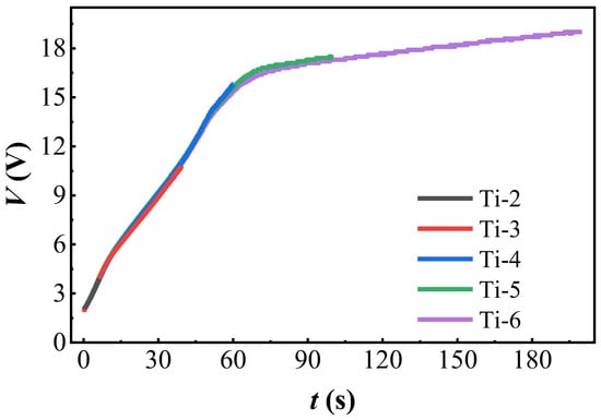
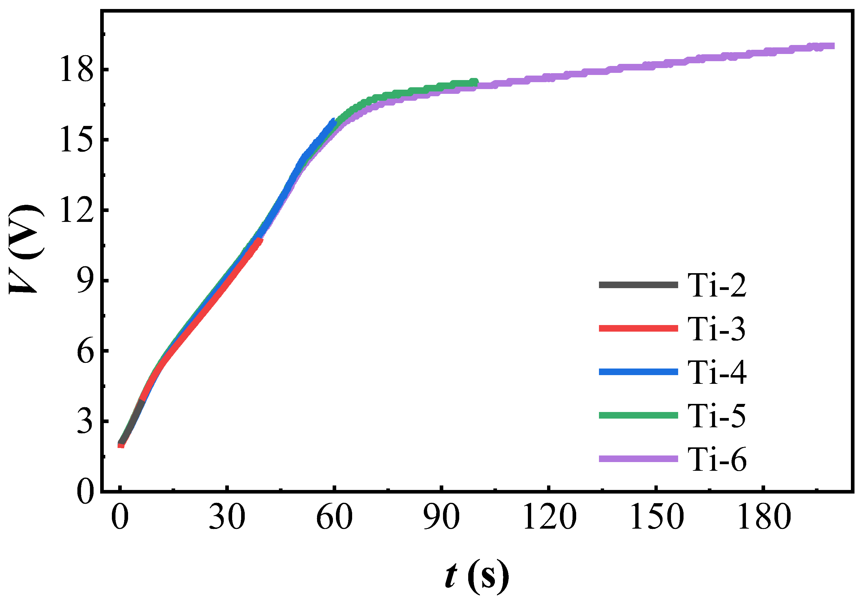
Figure 1 shows the V–t curves recorded during galvanostatic anodic oxidation of samples Ti-2 to Ti-6 at a current density of 1 mA/cm2. All samples exhibit similar trends. Immediately after the current is applied, the voltage rises rapidly as the pre-existing native oxide film thickens. Subsequently, the voltage increases more gradually as the anodic oxide layer grows under a quasi-steady electric field across the oxide. The cutoff voltage Vocv coincides with the maximum voltage attained during each anodization run and is 3.89 V, 10.77 V, 15.81 V, 17.45 V, and 19.03 V for Ti-2 to Ti-6, respectively. The corresponding oxidation times are 6 s, 40 s, 60 s, 100 s, and 200 s. For clarity, these parameters are summarized in Table 1.
Figure 1.
V–t curves for the anodic oxidation of Ti thin films.
Table 1.
Anodic oxidation parameters.
The initial voltage at the onset of anodization is approximately 2 V; while this measured terminal voltage includes the ohmic drop across the electrolyte, the distinct initial surge is primarily attributed to the presence of a pre-existing native oxide layer formed in air [43]. Using the linear relation between total oxide thickness and Vocv extracted from ellipsometry (Section 3.4), this native oxide thickness is estimated to be in the range of 0.7–3.5 nm.
3.2. Effect of Anodic Oxidation on Ultraviolet Reflectance
The spectral reflectance of the films was measured using a UH4150 spectrophotometer (integrating sphere) from Hitachi at a scanning speed of 300 nm/min. The wavelength interval was set to 1 nm for all samples, except for Ti-2 and Ti-4, for which a finer sampling interval of 0.5 nm was used. The measurement range was 270–1000 nm.
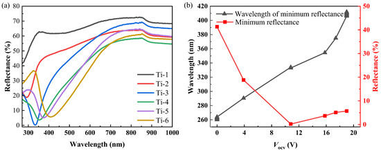
Figure 2a compares the reflectance spectra of samples Ti-1 to Ti-6. The non-anodized reference sample Ti-1 exhibits relatively high reflectance across the entire wavelength range. In contrast, all anodized samples (Ti-2 to Ti-6) show a pronounced reduction in reflectance, indicating that the formation of a TiOx top layer modifies the interference conditions and enhances absorption in the Ti/TiOx stack.
Figure 2.
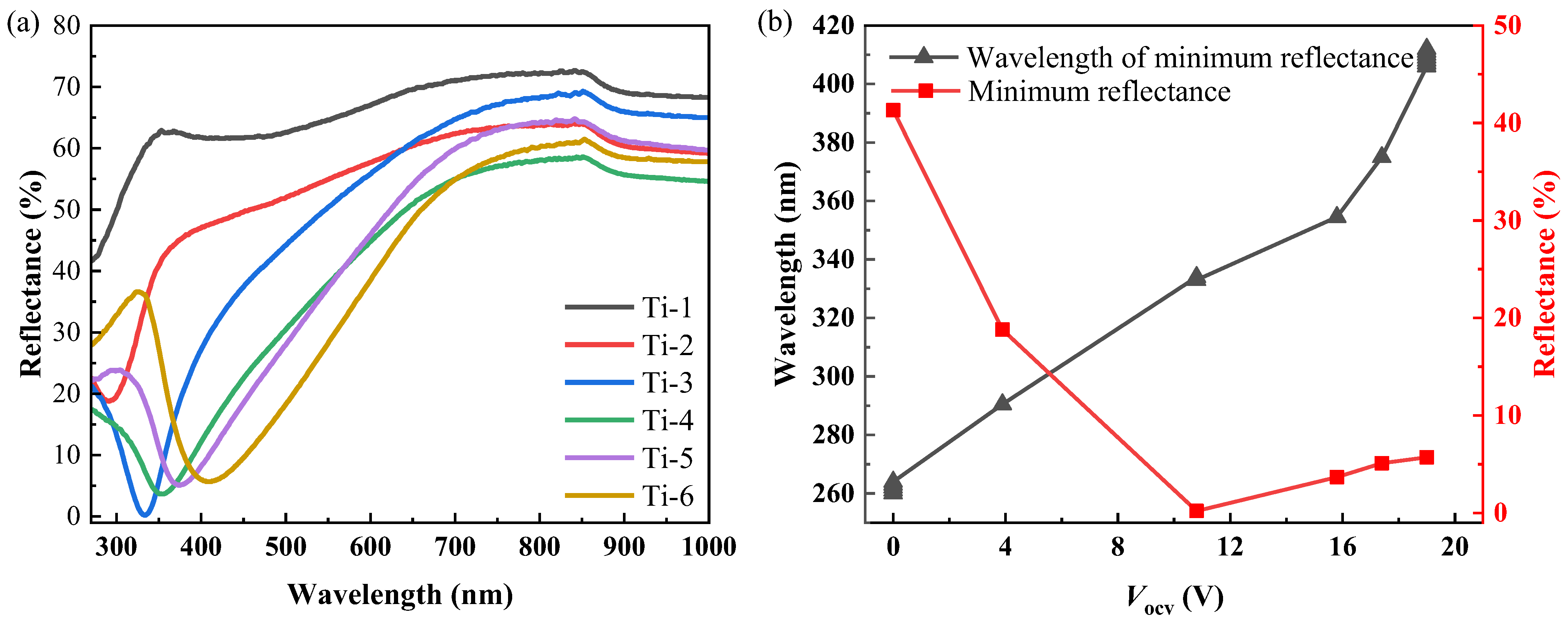
(a) Reflectance of Ti thin films. (b) Relationship between wavelength and Vocv at the minimum reflectance and the relationship between minimum reflectance values and Vocv.
In the near-UV region, each anodized sample exhibits a well-defined reflectance minimum. The wavelength corresponding to this minimum and the minimum reflectance value are plotted as functions of Vocv in Figure 2b. As Vocv increases, the wavelength of minimum reflectance shifts monotonically to longer wavelengths, i.e., a clear redshift is observed. This behavior is consistent with the increasing optical thickness of the TiOx layer: as the oxide grows thicker, the interference condition between reflections at the TiOx/air and TiOx/Ti interfaces changes, shifting the destructive interference toward longer wavelengths.
Among the first series of samples, Ti-3 (Vocv = 10.77 V) shows the lowest reflectance. The minimum reflectance is 0.2% at 334 nm, and the reflectance remains below 1% in the 328–339 nm range and below 2% in the 324–342 nm range. These results demonstrate that anodic oxidation can yield extremely low UV reflectance using only a single sputtered Ti layer and its electrochemically grown oxide, without the need for additional dielectric coatings.
3.3. Cross-Sectional Microstructure and Composition
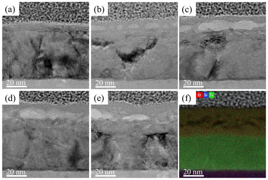
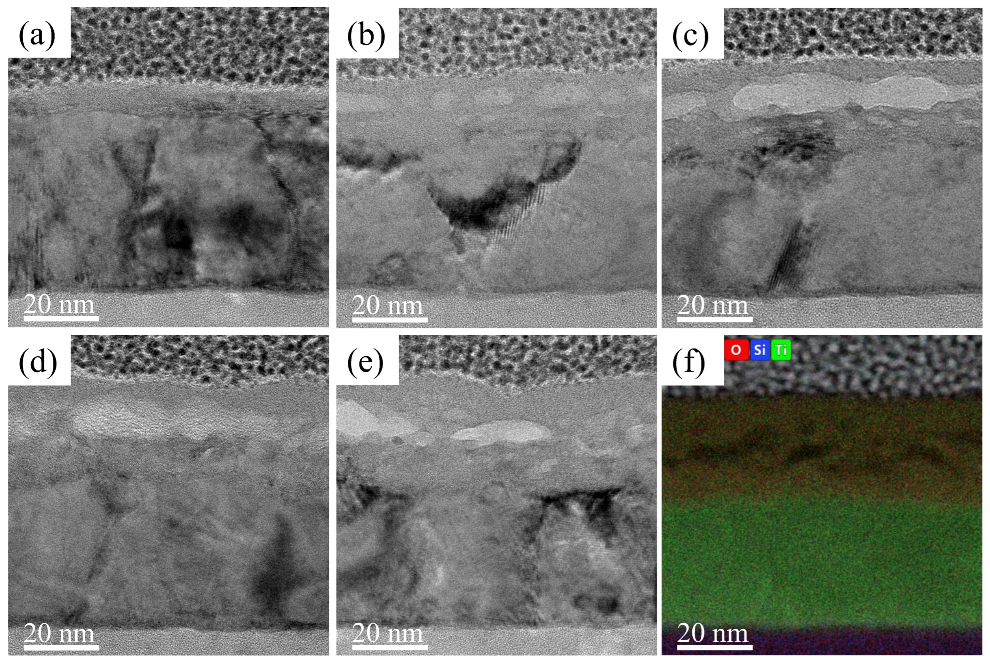
To elucidate the structural evolution induced by anodic oxidation, cross-sectional TEM analysis was performed on samples Ti-2 to Ti-6. Representative micrographs are presented in Figure 3a–e. In all anodized samples, the Ti film is transformed into a two-layer structure on top of the SiO2/Si substrate: a top TiOx layer and an underlying metallic Ti layer. The Si substrate is outside the field of view in some micrographs, but is known from the stack design. Figure 3f displays an energy-dispersive spectroscopy (EDS) elemental map for Ti-6. The oxygen-rich top layer is attributed to TiOx, the middle layer corresponds primarily to metallic Ti with only trace oxygen, and the bottom layer corresponds to SiO2. These observations confirm the expected TiOx/Ti/SiO2 trilayer structure.
Figure 3.
Cross-sectional TEM images of Ti thin films: (a–e) TEM images of samples Ti-2 to Ti-6, respectively. (f) EDS elemental map of Ti-6.
The interfaces between these layers are not atomically sharp; both composition and image contrast exhibit gradual variation across the transition regions, and each layer exhibits some thickness undulation. A qualitative comparison of the cross-sectional TEM images (Figure 3a–e) suggests that this interfacial undulation becomes more pronounced with increasing anodic oxidation cutoff voltage (Vocv). As a consequence, layer thicknesses extracted from TEM images carry an intrinsic uncertainty and should be interpreted as average values over the analyzed region rather than precise local thicknesses.
The TEM images also reveal that, for most anodized samples, parts of the TiOx layer exhibit a regular lattice contrast, indicating local crystallization. An exception is sample Ti-2, whose TiOx layer remains amorphous, as confirmed by the absence of diffraction spots in the Fourier transform analysis. The degree of crystallization varies not only from sample to sample but also with depth within the same sample. Between crystallized regions, the material remains amorphous. This spatially heterogeneous microstructure implies that the optical properties of the TiOx layer can vary locally on the nanoscale, even though an effective-medium description remains valid for macroscopic optical modeling.
3.4. Optical Constants and Thickness Evolution from Ellipsometry
Despite the microscopic inhomogeneity observed by TEM, the TiOx layer can be treated as an effective homogeneous medium when modeling the macroscopic optical response. To quantify its effective optical constants and thickness, we fitted spectroscopic ellipsometry data using a multilayer model consisting of TiOx, Ti, SiO2, and Si.
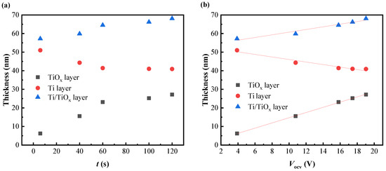
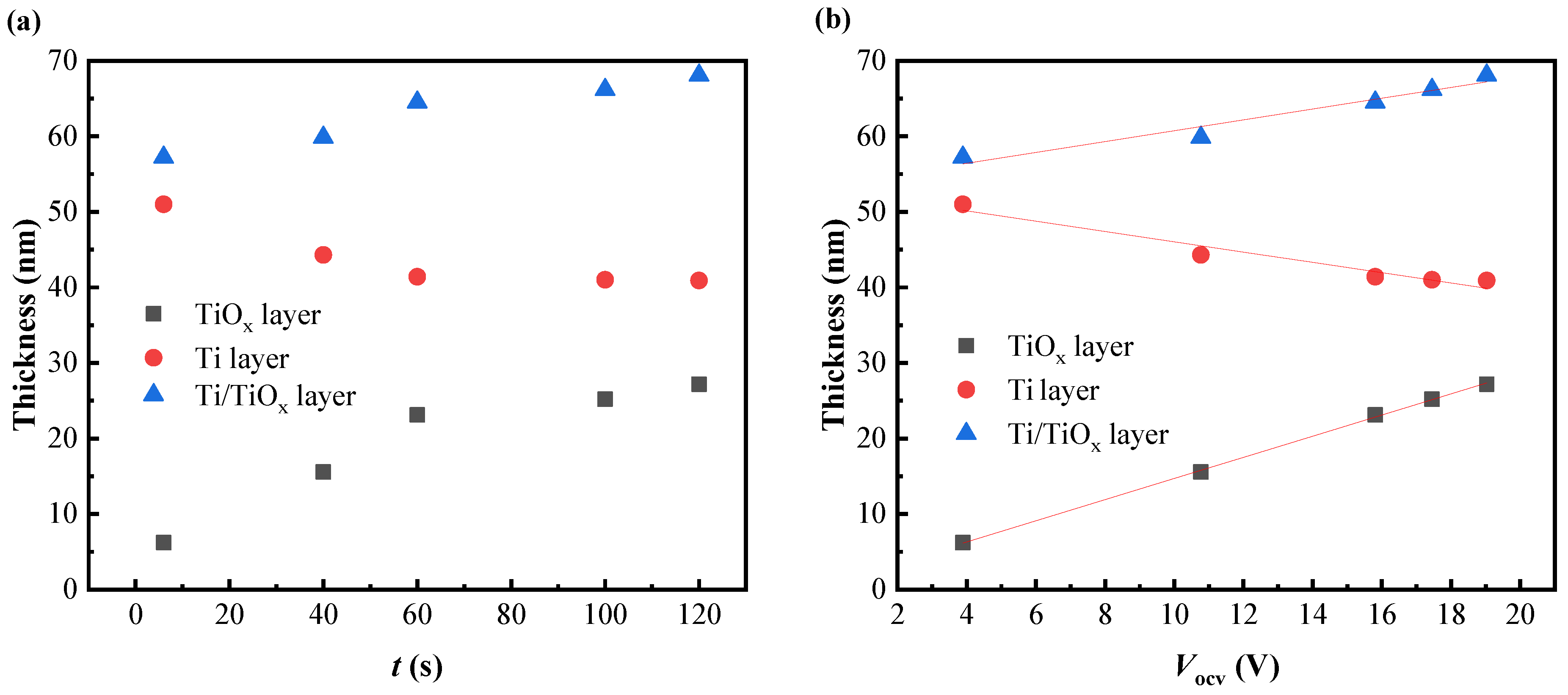
Ellipsometry measurements were performed using a Woollam M2000 ellipsometer (J.A. Woollam, Lincoln, NE, USA) over the 270–1000 nm wavelength range, with an average wavelength step of 1.3 nm. Thickness values obtained from TEM served as initial guesses for the model. Figure 4a,b show the fitted thicknesses of the TiOx layer, the remaining Ti layer, and the total Ti/TiOx stack as functions of oxidation time and Vocv, respectively. Both the TiOx thickness and the total thickness increase with longer anodization time and higher Vocv. Over the investigated range, the dependence on Vocv is approximately linear. Least-squares fits yield the following relations for thickness (in nm):
Figure 4.
(a) Each layer thickness as a function of time and (b) each layer thickness as a function of Vocv. Thickness values were determined by ellipsometric fitting.
Ti thickness: dTi ≈ 52.8 − 0.68 Vocv;
TiOx thickness: dTiOx ≈ 0.70 + 1.40 Vocv;
Total Ti/TiOx thickness: dTotal ≈ 53.6 + 0.72 Vocv.
As Vocv increases, the TiOx layer grows while the remaining metallic Ti layer becomes thinner, consistent with the progressive oxidation of the Ti film. The fits indicate that, in the absence of anodization (Vocv = 0), the Ti thickness is about 52.8 nm, and the native TiOx layer thickness is at least 0.7 nm. Combined with the initial anodization voltage of ≈2 V (Figure 1), this suggests that the native oxide thickness lies between 0.7 and 3.5 nm.
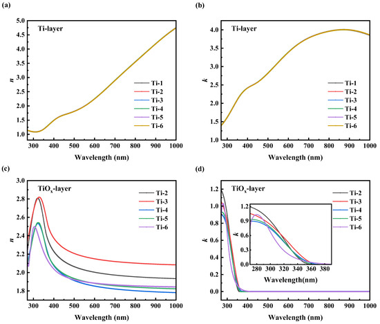
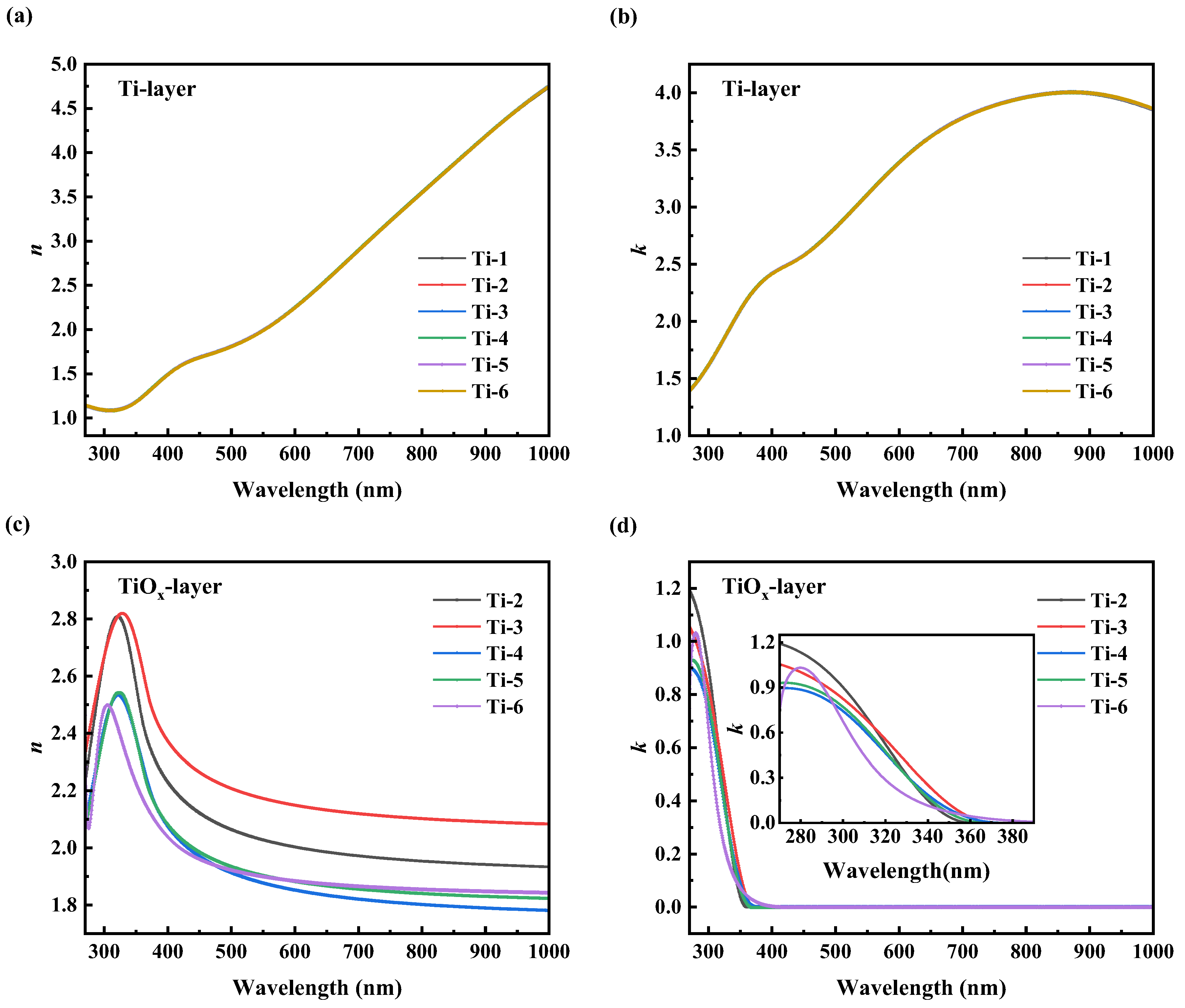
Figure 5 presents the wavelength-dependent refractive index n and extinction coefficient k of the Ti and TiOx layers for samples Ti-1 to Ti-6. For the Ti layer, both n and k show negligible variation with Vocv, indicating that the unoxidized portion of the film retains essentially the same optical properties as the as-deposited Ti layer. By contrast, the TiOx layer exhibits noticeable changes in its effective optical constants as Vocv increases, although these changes do not follow a simple monotonic trend. This behavior reflects the complex, heterogeneous nature of the anodic film. Specific phase identification via selected area electron diffraction proved challenging because the nucleated crystalline domains are nanometric in size and occupy a small volume fraction within the amorphous matrix. Consequently, the extracted n and k represent effective values of a composite medium consisting of the amorphous matrix, dispersed nanocrystallites, and sub-stoichiometric species (Ti3+, Ti2+). As established by previous depth-profiling XPS studies [40], such films exhibit a chemical gradient from stoichiometric TiO2 at the surface to conductive sub-oxides at the metal interface. The fluctuation in the optical constants thus arises from the varying volume fractions of these components and the compositional gradient. To evaluate the reliability of the extracted optical constants, we next compare FDTD simulations based on these values with the measured reflectance spectra.
Figure 5.
Refractive index (n) and extinction coefficient (k) of the Ti and TiOx layers for samples Ti-1 to Ti-6, extracted from ellipsometry: (a,b) n and k of the Ti layer; (c,d) corresponding values for the TiOx layer.
3.5. Superconducting Properties
Although the focus of this work is on the optical properties of anodically oxidized Ti/TiOx thin films, it is essential to confirm that the anodization process does not suppress the superconductivity of the Ti layer under conditions relevant for TES operation. The superconducting electrical properties directly determine key TES performance metrics.
The superconducting transition was characterized using a DRC200 adiabatic demagnetization refrigerator (STAR Cryoelectronics, Santa Fe, NM, USA), which provides a base temperature below 42 mK. Resistance–temperature (R–T) curves were measured in a constant-current mode of 10 μA using a Lakeshore 372 AC resistance bridge (Lake Shore Cryotronics, Westerville, OH, USA), with the voltage drop recorded in a four-wire configuration.
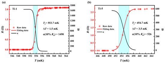
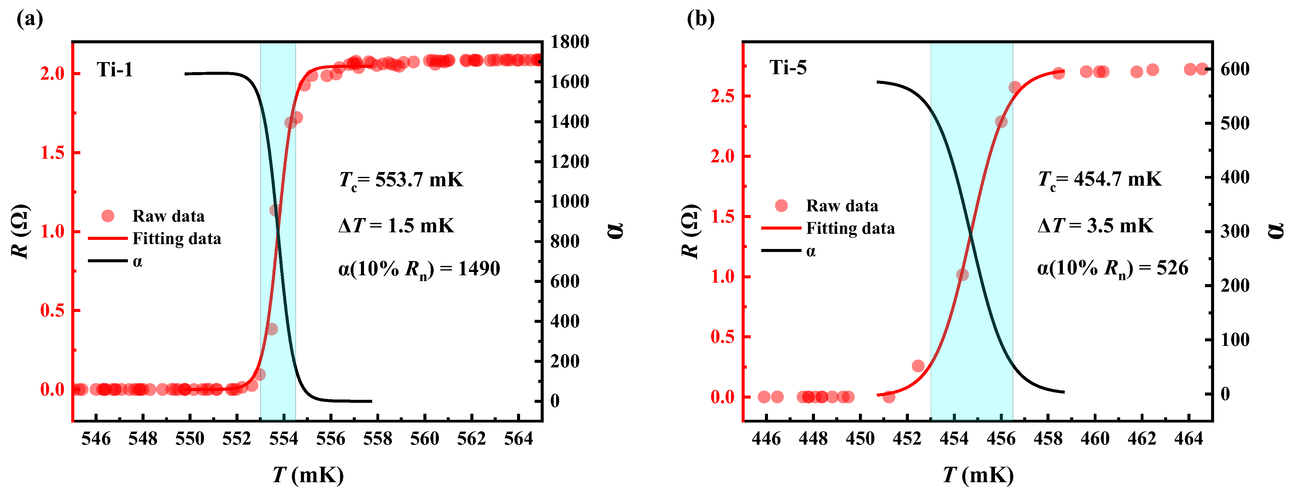
To assess the impact of anodization on superconducting transition, we analyzed the R–T characteristics of the non-anodized sample Ti-1 and a representative anodized sample Ti-5, which was subjected to a relatively high Vocv. The experimental data, along with the fitted transition curves and the calculated unitless logarithmic temperature sensitivity (), are presented in Figure 6.
Figure 6.
Superconducting transition characteristics of (a) the non-anodized sample Ti-1 and (b) the anodized sample Ti-5. The plots display the measured resistance versus temperature (R–T) data (left axis) and the calculated unitless logarithmic temperature sensitivity α (right axis). The solid lines represent the fitted transition curves used to determine the critical temperature (Tc), transition width (ΔT), and α. The colored regions represent the superconducting transition range.
First, regarding the critical temperature, the Tc of Ti-1 is 553.7 mK, whereas that of Ti-5 is 454.7 mK, corresponding to a decrease of 99 mK. This suppression of superconductivity can be understood from an electrochemical perspective: during anodization, the thickness of the metallic Ti substrate is reduced due to oxidation, and the resulting oxide layer may contain sub-stoichiometric regions that exhibit semiconducting-like electronic properties [44]. Such regions in close contact with the superconducting Ti can induce a superconducting proximity effect, which generally suppresses the overall superconducting performance, including a reduction in Tc. For TES applications, however, this reduction is beneficial as it lowers the heat capacity and thermal noise, thereby improving energy resolution. Furthermore, we evaluated the transition width ΔT, defined as the temperature interval between 10% and 90% of the normal state resistance (Rn) and α. As shown in Figure 6a, Ti-1 exhibits a very sharp transition with ΔT = 1.5 mK and a peak temperature sensitivity of α ≈ 1490 (at 10% Rn). In contrast, for the anodized Ti-5 shown in Figure 6b, the transition broadens to ΔT = 3.5 mK, and the sensitivity decreases to α ≈ 526. This broadening is likely attributed to slight spatial inhomogeneities introduced by the anodic oxidation process. Nevertheless, an α value of 526 remains sufficiently high for high-performance TES operation. Thus, the anodic oxidation process effectively tailors the optical response while maintaining a superconducting transition suitable for detector applications.
4. Simulation
To further interpret the experimental trends and validate the optical constants extracted from ellipsometry, we employed the FDTD method to simulate the reflectance spectra of the Ti thin-film samples. FDTD is a widely used time-domain numerical technique for solving Maxwell’s equations and modeling electromagnetic wave propagation, reflection, and refraction in complex multilayer structures.
The simulated structure consisted of a semi-infinite Si substrate, a 213 nm SiO2 layer, and the Ti and TiOx layers, with thicknesses and complex refractive indices taken from the ellipsometry fits. A normally incident plane wave with a wavelength range of 270–1000 nm was used as the light source, incident from the TiOx side toward the Si substrate. Monitors were placed above the TiOx layer to record the reflected power. The simulation mesh was set to 5 nm in the direction parallel to the film plane and 1 nm in the direction of light propagation. Periodic boundary conditions were applied in the in-plane directions to emulate an extended film.
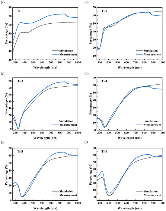
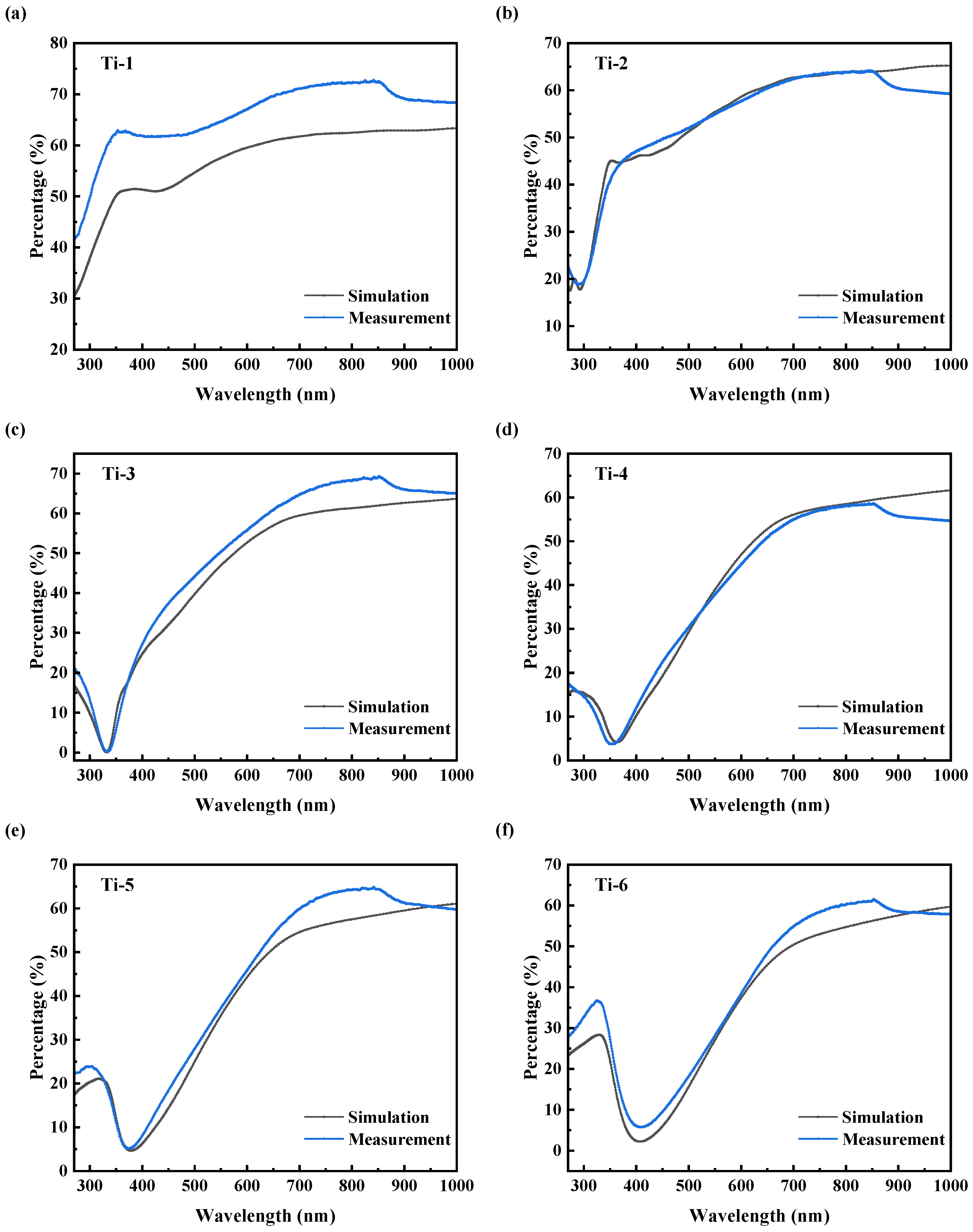
Figure 7 compares the experimental reflectance spectra with the FDTD simulations for samples Ti-1 to Ti-6. In each panel, the measured data (blue line) and simulated reflectance (black line) are shown together. For Ti-1 (Figure 7a), the simulation uses the Ti thickness extracted from ellipsometry; prior to this, the thickness had been estimated from deposition time and rate and had not been confirmed by TEM. For this sample, the agreement between experiment and simulation is relatively poor. This discrepancy is mainly attributed to the simplified model, which neglects the thin native TiOx layer present on the surface of the non-anodized Ti film. A similar mismatch is observed for Ti-6, where the thickest anodic oxide and the pronounced interface irregularity at the Ti and TiOx (visible in Figure 3e) are not fully captured by the idealized multilayer model.
Figure 7.
Comparison of FDTD simulation results and experimental optical reflectance spectra for samples Ti-1 through Ti-6. In each panel, the blue line represents the measured reflectance, and the black line represents the simulated reflectance. The panels correspond to individual samples as follows: (a) Ti-1, (b) Ti-2, (c) Ti-3, (d) Ti-4, (e) Ti-5, and (f) Ti-6.
In contrast, for samples Ti-2 to Ti-5, the simulated spectra exhibit good agreement with the experimental data across most of the measurement range. These results indicate that representing the TiOx layer as a single effective homogeneous layer is adequate for reproducing the macroscopic reflectance behavior under the oxidation conditions studied here. They also provide independent validation that the optical constants obtained from the ellipsometry fits are physically meaningful and can be used for optical design and optimization.
5. Discussion
As shown in Section 3.2, Ti-3 exhibits particularly low UV reflectance within a relatively narrow wavelength band. To gain deeper insight into which anodization parameters most strongly influence the optical response, we fabricated a second series of samples (Ti-7 to Ti-19) at a reduced anodic oxidation current density of 0.5 mA/cm2. The oxidation times were varied from 20 to 400 s, resulting in Vocv values in the range of 5.83–15.75 V. The lower current density slowed the voltage rise and provided finer control over the electrochemical process.
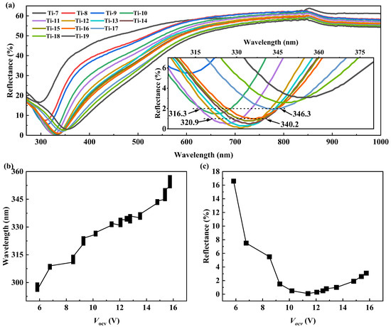
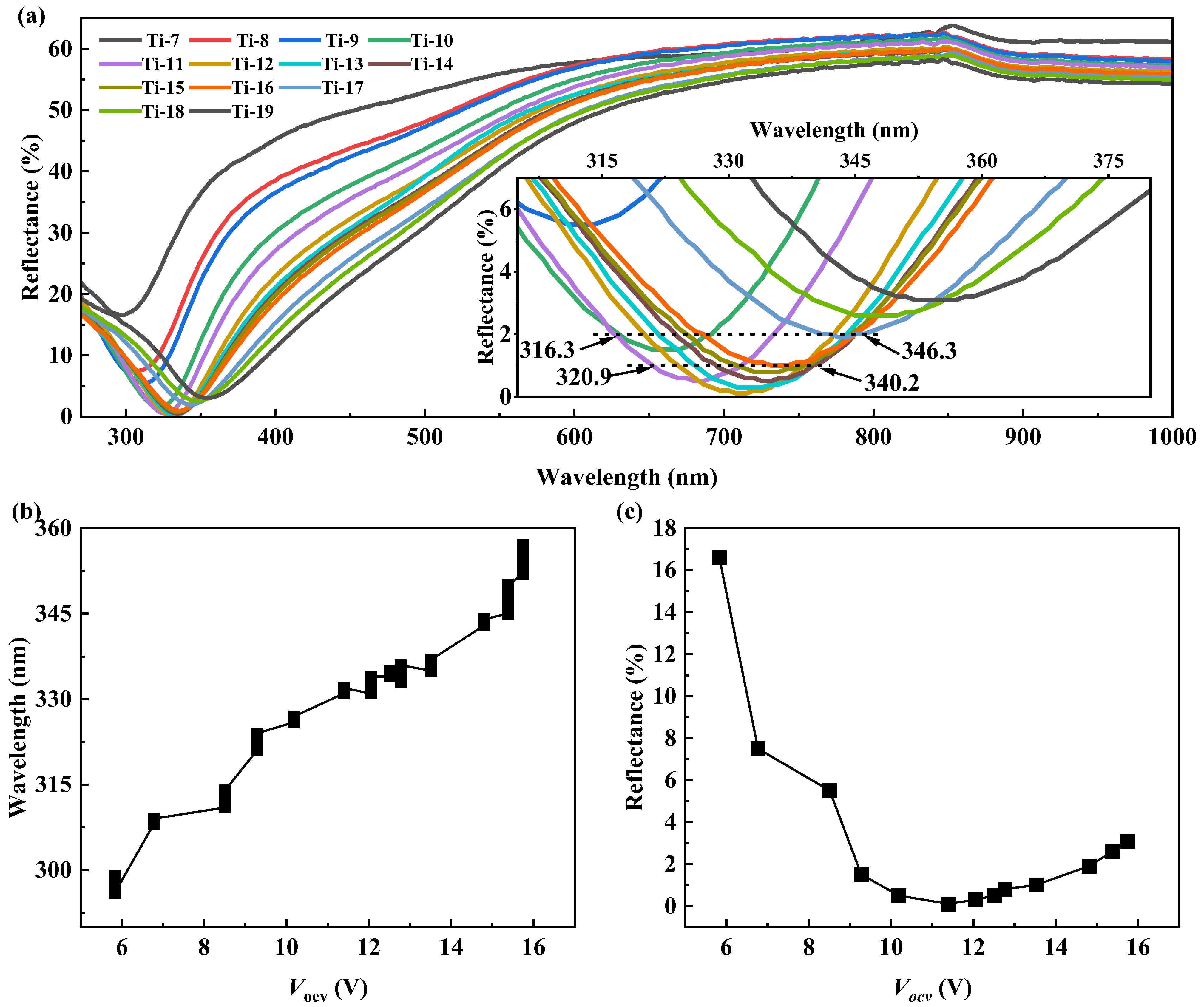
Figure 8a shows the reflectance spectra of samples Ti-7 to Ti-19. Because the curves partially overlap in the UV region, the inset displays an enlarged view of the 305–380 nm range. For samples Ti-11 to Ti-15, the minimum reflectance is below 1%. Under the preparation conditions used here, reflectance values below 1% are obtained in the 320.9–340.2 nm wavelength range and below 2% in the 316.3–346.3 nm range. Figure 8b,c summarize how the wavelength of the reflectance minimum and the minimum reflectance value depend on Vocv. As Vocv increases, the reflectance minimum shifts toward longer wavelengths, consistent with the results from the first sample series at 1 mA/cm2.
Figure 8.
(a) Reflectance characterization of samples Ti-7 to Ti-19, the inset shows an enlarged view of the 305–380 nm range; (b) wavelength corresponding to the minimum reflectance as a function of Vocv; (c) minimum reflectance as a function of Vocv.
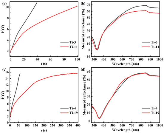
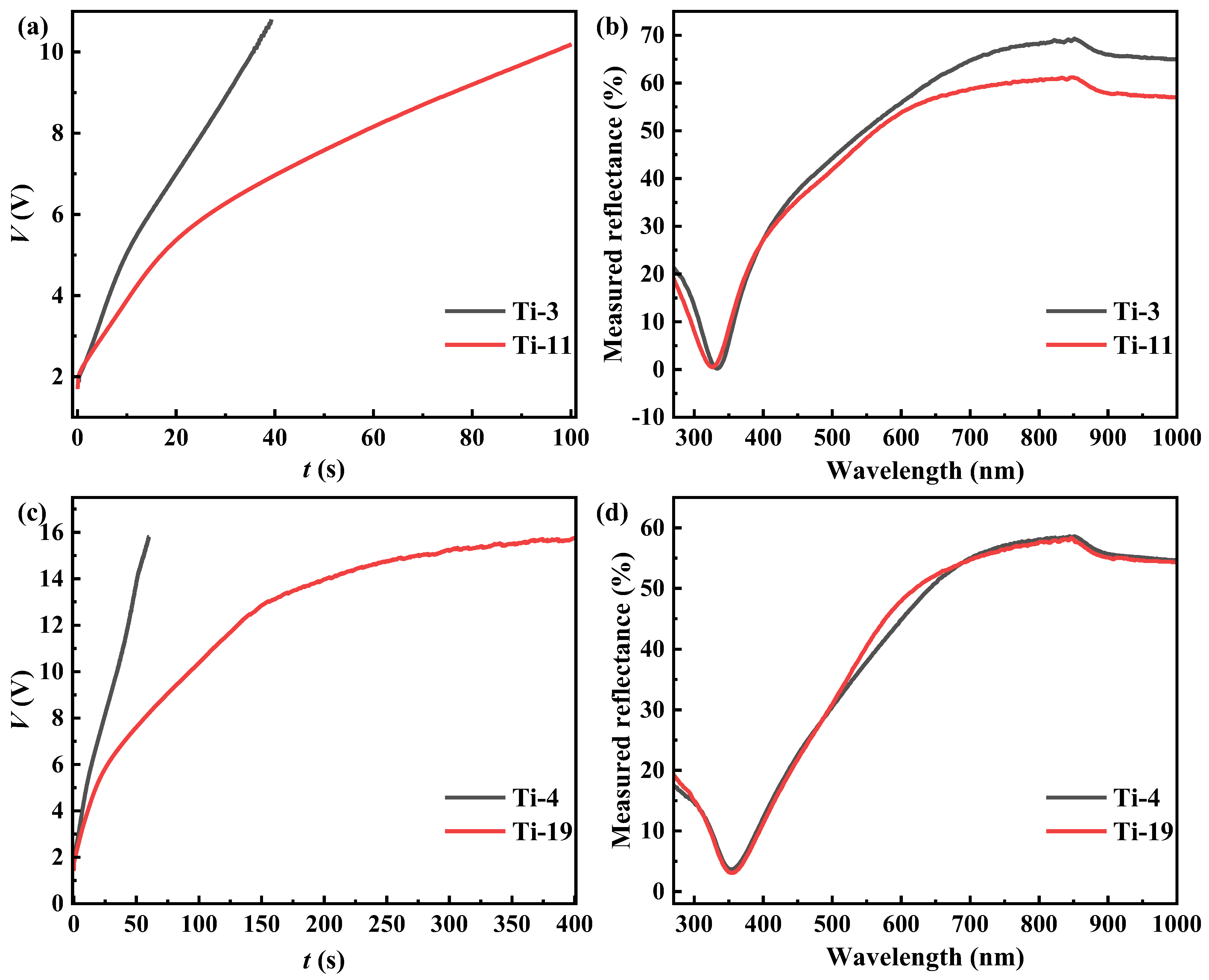
To disentangle the respective influences of current density, Vocv, and oxidation time on the optical properties, we compared sample pairs with closely matched Vocv but different current densities and oxidation durations. Specifically, samples Ti-3 and Ti-11 form one pair, and samples Ti-4 and Ti-19 form another. The corresponding parameters are (10.77 V, 40 s, 1 mA/cm2) and (10.19 V, 100 s, 0.5 mA/cm2) for Ti-3 and Ti-11, and (15.81 V, 60 s, 1 mA/cm2) and (15.75 V, 400 s, 0.5 mA/cm2) for Ti-4 and Ti-19. The Vocv differences within each pair are only 0.58 V and 0.06 V, respectively.
Figure 9 compares the V–t curves and reflectance spectra for these two pairs. For the first pair (Ti-3 and Ti-11), the reflectance spectra overlap very well in the UV range, while deviations are more noticeable at longer wavelengths. For the second pair (Ti-4 and Ti-19), which have nearly identical Vocv, the agreement is good over a broad spectral range. These observations indicate that Vocv is more decisive than current density or oxidation time in determining the final optical response, at least within the parameter space explored in this study. Physically, this is reasonable because Vocv sets the maximum electric field across the oxide layer and thus strongly influences ionic transport and electrochemical reaction rates, which ultimately determine the thickness, density, and stoichiometry of the TiOx film. Under galvanostatic conditions, Vocv can therefore be regarded as an effective control parameter that encapsulates much of the complexity of the anodic growth process.
Figure 9.
(a) Comparison of anodic oxidation V–t curves of samples Ti-3 and Ti-11; (b) comparison of reflectance of samples Ti-3 and Ti-11; (c) comparison of anodic oxidation V–t curves of samples Ti-4 and Ti-19; (d) comparison of reflectance between samples Ti-4 and Ti-19.
From a practical standpoint, the anodic oxidation approach demonstrated here has several advantages for TES device fabrication when compared with conventional methods for depositing TiOx (such as atomic layer deposition or electron-beam evaporation). First, it is experimentally straightforward, with low cost, and performed at room temperature using standard electrochemical equipment. Second, it offers in situ and post-fabrication tunability: as shown by the dependence of the reflectance minimum on Vocv, the optical response can be adjusted by simply varying the terminal voltage in the anodization process. This tunability implies that the reflectance of a superconducting Ti film can be fine-tuned even after other device layers have been fabricated, which is often difficult using purely vacuum-based coating approaches. Together, these features—simplicity, compatibility with microfabrication, and voltage-controlled tunability—make anodic oxidation an attractive strategy for integrating optical optimization into the design of Ti-based TES coatings and absorbers.
6. Conclusions
In this work, we investigated the anodic oxidation of superconducting Ti thin films as a means to control their UV reflectance for TES applications. By combining reflectance spectroscopy, TEM, spectroscopic ellipsometry, and FDTD simulations, we obtained the following main conclusions:
Control of UV reflectance via Vocv: Anodic oxidation in an ammonium pentaborate-based electrolyte significantly reduces the UV reflectance of Ti films and induces a monotonic redshift of the reflectance minimum with increasing Vocv. Reflectance values below 1% in the 320.9–340.2 nm range and below 2% in the 316.3–346.3 nm range are achieved under optimized conditions.
Structural and optical evolution of the TiOx layer: Cross-sectional TEM and EDS confirm the formation of a TiOx/Ti/SiO2 trilayer structure after anodization. The TiOx layer is structurally inhomogeneous, with amorphous and locally crystalline regions. Nevertheless, spectroscopic ellipsometry shows that it can be treated as an effective homogeneous layer for optical modeling, and the extracted optical constants reproduce the measured reflectance when used in FDTD simulations.
Vocv as a key design parameter: Comparison of samples prepared at different current densities but similar Vocv demonstrates that Vocv is the dominant anodization parameter governing the optical response, because it dictates the thickness and effective optical properties of the anodic TiOx layer under galvanostatic conditions.
Compatibility with TES operation: Superconducting transition measurements confirm that anodically oxidized Ti films remain superconducting, with Tc reduced by about 100 mK under the conditions studied. Such a decrease in Tc can be advantageous for TES energy resolution, highlighting that anodic oxidation can simultaneously tune both optical and superconducting properties.
Overall, these findings establish anodic oxidation as a practical and flexible approach for engineering the UV reflectance of Ti films used in TES devices. By selecting suitable Vocv values, it is possible to design Ti/TiOx coatings with targeted reflectance minima and to integrate this tuning into TES absorber and cavity designs to maximize photon absorptance and thereby enhance the potential QE in the UV range. Future work will focus on (i) a more systematic study of the relationship between Vocv and Tc, including microscopic mechanisms, and (ii) full TES device fabrication and characterization to directly correlate optical absorption with detector metrics such as QE and energy resolution.
Author Contributions
Conceptualization, X.W. and J.C.; methodology, X.X., X.W. and J.C.; software, J.C.; validation, J.C., and H.G.; formal analysis, W.L.; investigation, W.L. and J.C.; resources, J.C. and H.G.; data curation, W.L.; writing—original draft preparation, W.L.; writing—review and editing, X.W. and W.L.; visualization, W.L.; supervision, J.L. and Z.Z.; project administration, X.X.; funding acquisition, J.L. and X.W. All authors have read and agreed to the published version of the manuscript.
Funding
This work was supported by the National Key R&D Program of China (Grant No. 2022YFF0608303), the National Natural Science Foundation of China (Grant No. 12303101), and the National Institute of Metrology Program (Grant No. AKYJJ2403).
Institutional Review Board Statement
Not applicable.
Informed Consent Statement
Not applicable.
Data Availability Statement
Data are contained within the article. Further inquiries can be directed to the corresponding authors.
Conflicts of Interest
The authors declare no conflicts of interest.
References
- Luo, Q.; Zhong, J.; Miao, W.; Li, F.; Wang, Q.; Ding, J.; Wu, F.; Wang, Z.; Zhou, K.; Ren, Y.; et al. A 220 GHz Superconducting Titanium Transition Edge Sensor Array Developed for Cosmic Microwave Background Experiments. Supercond. Sci. Technol. 2023, 36, 115004. [Google Scholar] [CrossRef] [Scilit]
- Xu, Y.; Li, Z.; Li, Y.; Zhang, Y.; Li, X.; Lu, X.; Liao, G.; Li, Q.; Lu, F.; Zhang, L.; et al. Design and Characterization of a 90 GHz CMB TES Bolometer. Exp. Astron. 2024, 57, 8. [Google Scholar] [CrossRef] [Scilit]
- Mangu, A.; Westbrook, B.; Beckman, S.; Corbett, L.; Crowley, K.T.; Dutcher, D.; Johnson, B.R.; Lee, A.T.; Kabra, V.; Prasad, B.; et al. The Simons Observatory: Design, Optimization, and Performance of Low-Frequency Detectors. J. Low Temp. Phys. 2025, 218, 21–28. [Google Scholar] [CrossRef] [Scilit] [PubMed]
- Fukuda, D.; Fujii, G.; Numata, T.; Amemiya, K.; Yoshizawa, A.; Tsuchida, H.; Fujino, H.; Ishii, H.; Itatani, T.; Inoue, S.; et al. Titanium-based Transition-edge Photon Number Resolving Detector with 98% Detection Efficiency with Index-matched Small-gap Fiber Coupling. Opt. Express 2011, 19, 870–875. [Google Scholar] [CrossRef] [Scilit] [PubMed]
- Carter, F.W.; Santavicca, D.F.; Prober, D.E. A Plasmonic Antenna-coupled Superconducting Near-IR Photon Detector. Opt. Express 2014, 22, 22062–22071. [Google Scholar] [CrossRef] [Scilit]
- Hattori, K.; Konno, T.; Miura, Y.; Takasu, S.; Fukuda, D. An Optical Transition-edge Sensor with High Energy Resolution. Supercond. Sci. Technol. 2022, 35, 095002. [Google Scholar] [CrossRef] [Scilit]
- Xu, X.; Sun, X.; Chen, J.; Rajteri, M.; Garrone, H.; Pepe, C.; Li, W.; Li, J.; Zhang, M.; Bu, T.; et al. Development of Ti/Au Transition-Edge Sensors for Single-Photon Detection. IEEE Trans. Appl. Supercond. 2024, 34, 2100104. [Google Scholar] [CrossRef] [Scilit]
- Smith, S.J.; Adams, J.S.; Bailey, C.N.; Bandler, S.R.; Chervenak, J.A.; Eckart, M.E.; Finkbeiner, F.M.; Kelley, R.L.; Kilbourne, C.A.; Porter, F.S.; et al. Small Pitch Transition-Edge Sensors with Broadband High Spectral Resolution for Solar Physics. J. Low Temp. Phys. 2012, 167, 168–175. [Google Scholar] [CrossRef] [Scilit]
- Bennett, D.A.; Horansky, R.D.; Schmidt, D.R.; Hoover, A.S.; Winkler, R.; Alpert, B.K.; Beall, J.A.; Doriese, W.B.; Fowler, J.W.; Fitzgerald, C.P.; et al. A High Resolution Gamma-Ray Spectrometer Based on Superconducting Microcalorimeters. Rev. Sci. Instrum. 2012, 83, 093113. [Google Scholar] [CrossRef] [Scilit]
- Nagayoshi, K.; Ridder, M.L.; Bruijn, M.P.; Gottardi, L.; Taralli, E.; Khosropanah, P.; Akamatsu, H.; Visser, S.; Gao, J.R. Development of a Ti/Au TES Microcalorimeter Array as a Backup Sensor for the Athena/X-IFU Instrument. J. Low Temp. Phys. 2020, 199, 943–948. [Google Scholar] [CrossRef] [Scilit]
- Akamatsu, H.; Gottardi, L.; van der Kuur, J.; de Vries, C.P.; Bruijn, M.P.; Chervenak, J.A.; Kiviranta, M.; van den Linden, A.J.; Jackson, B.D.; Miniussi, A.; et al. Progress in the Development of Frequency-Domain Multiplexing for the X-ray Integral Field Unit on Board the Athena Mission. J. Low Temp. Phys. 2020, 199, 737–744. [Google Scholar] [CrossRef] [Scilit]
- Tsuruta, T.; Iyomoto, N.; Asagawa, S.; Hamamura, Y.; Nishida, Y.; Maehata, K.; Mitsuda, K.; Hayashi, T. Transition Edge Sensor Microcalorimeter With Bismuth Absorber for Gamma-Ray Measurement. IEEE Trans. Appl. Supercond. 2021, 31, 2102104. [Google Scholar] [CrossRef] [Scilit]
- Smith, S.J.; Adams, J.S.; Bandler, S.R.; Beaumont, S.; Chervenak, J.A.; Denison, E.V.; Doriese, W.B.; Durkin, M.; Finkbeiner, F.M.; Fowler, J.W.; et al. Performance of a Broad-Band, High-Resolution, Transition-Edge Sensor Spectrometer for X-ray Astrophysics. IEEE Trans. Appl. Supercond. 2021, 31, 2100806. [Google Scholar] [CrossRef] [Scilit]
- Zhang, S.; Xia, J.; Sun, T.; Wu, W.; Wu, B.; Wang, Y.; Cantor, R.; Han, K.; Zhou, X.; Liu, H.; et al. Transition Edge Sensor-Based Detector: From X-Ray to Γ-Ray. Nucl. Sci. Tech. 2022, 33, 84. [Google Scholar] [CrossRef] [Scilit]
- Wang, H.; Lv, Y.; Li, D.; Zhao, Y.; Gao, B.; Wang, Z. Transition-edge Sensors using Mo/Au/Au Tri-layer Films. Chin. Phys. B 2023, 32, 028501. [Google Scholar] [CrossRef] [Scilit]
- Kikuchi, T.; Fujii, G.; Hayakawa, R.; Smith, R.; Hirayama, F.; Sato, Y.; Kohjiro, S.; Ukibe, M.; Ohno, M.; Sato, A.; et al. A 320-keV Spectrometer Based on 8-Pixel Transition Edge Sensor With Trilayer Membrane and Novel Numerical Analysis. IEEE Trans. Appl. Supercond. 2023, 33, 2101706. [Google Scholar] [CrossRef] [Scilit]
- Barret, D.; Albouys, V.; Herder, J.-W.d.; Piro, L.; Cappi, M. The Athena X-ray Integral Field Unit: A Consolidated Design for the System Requirement Review of the Preliminary Definition Phase. Exp. Astron. 2023, 55, 373–426. [Google Scholar] [CrossRef] [Scilit]
- Croce, M.P.; Bacrania, M.K.; Bond, E.M.; Dry, D.E.; Klingensmith, A.L.; Moody, W.A.; LaMont, S.P.; Rabin, M.W.; Rim, J.H.; Beall, J.A.; et al. Superconducting Transition-Edge Sensor Microcalorimeters for Ultra-High Resolution Alpha-Particle Spectrometry. IEEE Trans. Appl. Supercond. 2011, 21, 207–210. [Google Scholar] [CrossRef] [Scilit]
- Croce, M.; Bacrania, M.; Bond, E.; Dry, D.; Moody, W.A.; Rabin, M.; Bennett, D.; Hilton, G.; Horansky, R.; Kotsubo, V.; et al. Ultra-high Resolution Alpha Particle Spectrometry with Transition-Edge Sensor Microcalorimeters. J. Low Temp. Phys. 2012, 167, 955–960. [Google Scholar] [CrossRef] [Scilit]
- Patel, K.M.; Withington, S.; Shard, A.G.; Goldie, D.J.; Thomas, C.N. Electron Spectroscopy using Transition-edge Sensors. J. Appl. Phys. 2024, 135, 224504. [Google Scholar] [CrossRef] [Scilit]
- Szypryt, P.; O’Neil, G.C.; Takacs, E.; Tan, J.N.; Buechele, S.W.; Naing, A.S.; Bennett, D.A.; Doriese, W.B.; Durkin, M.; Fowler, J.W.; et al. A Transition-edge Sensor-based x-ray Spectrometer for the Study of Highly Charged Ions at the National Institute of Standards and Technology Electron Beam Ion Trap. Rev. Sci. Instrum. 2019, 90, 123107. [Google Scholar] [CrossRef] [Scilit] [PubMed]
- Joe, Y.I.; Fang, Y.; Lee, S.; Sun, S.X.L.; de la Pena, G.A.; Doriese, W.B.; Morgan, K.M.; Fowler, J.W.; Vale, L.R.; Rodolakis, F.; et al. Resonant Soft X-Ray Scattering from Stripe-Ordered La2-xBaxCuO4 Detected by a Transition-Edge Sensor Array Detector. Phys. Rev. Appl. 2020, 13, 034026. [Google Scholar] [CrossRef] [Scilit]
- Hashimoto, T.; Bennett, D.A.; Doriese, W.B.; Durkin, M.S.; Fowler, J.W.; Gard, J.D.; Hayakawa, R.; Hayashi, T.; Hilton, G.C.; Ichinohe, Y.; et al. Integration of a TES-based X-ray Spectrometer in a Kaonic Atom Experiment. J. Low Temp. Phys. 2020, 199, 1018–1026. [Google Scholar] [CrossRef] [Scilit]
- Szypryt, P.; Bennett, D.A.; Boone, W.J.; Dagel, A.L.; Dalton, G.; Doriese, W.B.; Durkin, M.; Fowler, J.W.; Garboczi, E.J.; Gard, J.D.; et al. Design of a 3000-Pixel Transition-Edge Sensor X-Ray Spectrometer for Microcircuit Tomography. IEEE Trans. Appl. Supercond. 2021, 31, 2100405. [Google Scholar] [CrossRef] [Scilit]
- Eckart, M.E.; Beiersdorfer, P.; Brown, G.V.; Den Hartog, D.J.; Hell, N.; Kelley, R.L.; Kilbourne, C.A.; Magee, E.W.; Mangoba, A.E.Y.; Nornberg, M.D.; et al. Microcalorimeter Measurement of X-ray Spectra from a High-Temperature Magnetically Confined Plasma. Rev. Sci. Instrum. 2021, 92, 063520. [Google Scholar] [CrossRef] [Scilit]
- Okumura, T.; AzumaG, T.; Bennett, D.A.; Caradonna, P.; Chiu, I.; Doriese, W.B.; Durkin, M.S.; Fowler, J.W.; Gard, J.D.; Hashimoto, T.; et al. Deexcitation Dynamics of Muonic Atoms Revealed by High-Precision Spectroscopy of Electronic K X Rays. Phys. Rev. Lett. 2021, 127, 053001. [Google Scholar] [CrossRef] [Scilit]
- Cabrera, B.; Clarke, R.M.; Colling, P.; Miller, A.J.; Nam, S.; Romani, R.W. Detection of single infrared, optical, and ultraviolet photons using superconducting transition edge sensors. Appl. Phys. Lett. 1998, 73, 735–737. [Google Scholar] [CrossRef] [Scilit]
- Miller, A.J.; Cabrera, B.; Romani, R.W.; Martinis, J.; Nam, S.W.; Weld, D.M.; Castle, P. Cryogenic IR/optical/UV fast spectrophotometers for the study of time-variable astronomical sources. In Proceedings of the Infrared Spaceborne Remote Sensing VIII, San Diego, CA, USA, 16 November 2000; pp. 278–284. [Google Scholar]
- Burney, J.; Bay, T.J.; Barral, J.; Brink, P.L.; Cabrera, B.; Castle, J.P.; Miller, A.J.; Nam, S.; Rosenberg, D.; Romani, R.W. Transition-edge Sensor Arrays for UV-optical-IR Astrophysics. Nucl. Instrum. Methods Phys. Res. Sect. A 2006, 559, 525–527. [Google Scholar] [CrossRef] [Scilit]
- Romani, R.W.; Miller, A.J.; Cabrera, B.; Nam, S.W.; Martinis, J.M. Phase-resolved crab studies with a cryogenic transition-edge sensor spectrophotometer. Astrophys. J. 2001, 563, 221. [Google Scholar] [CrossRef] [Scilit]
- Zhang, W.; Geng, Y.; Wang, Z.; Zhong, J.; Li, P.; Miao, W.; Ren, Y.; Yao, Q.; Wang, J.; Shi, S. Development of Titanium-Based Transition-Edge Single-Photon Detector. IEEE Trans. Appl. Supercond. 2019, 29, 2100505. [Google Scholar] [CrossRef] [Scilit]
- Zhang, W.; Wang, Z.; Zhong, J.; Li, P.; Geng, Y.; Miao, W.; Ren, Y.; Zhou, K.; Yao, Q.; Shi, S. Evidence for Controllable Reduction of Critical Temperature in Titanium TESs by Baking in Air. IEEE Trans. Appl. Supercond. 2021, 31, 2101205. [Google Scholar] [CrossRef] [Scilit]
- Zhang, W.; Wang, Z.; Li, P.; Zhong, J.; Ma, Q.; Feng, Z.; Zhou, K.; Miao, W.; Ren, Y.; Yao, Q.; et al. Tuning of Critical Temperature and Aging Effect of Ti Films For Superconducting Transition-Edge Sensors. J. Low Temp. Phys. 2024, 214, 106–112. [Google Scholar] [CrossRef] [Scilit]
- Chen, J.; Wang, Z.; Xu, D.; Qiao, H.; Li, J.; Zhong, Q.; Wang, S.; Zeng, J.; Cai, J.; Zhang, M.; et al. Optimization of Nb/Al-AlOx/Nb Josephson Junctions through Wafer-scale Anodic Oxidation: A Systematic Characterization and Performance Analysis. Supercond. Sci. Technol. 2023, 36, 105003. [Google Scholar] [CrossRef] [Scilit]
- Chowdhary, N.K.; Gougousi, T. Extracting the Optical Constants of Partially Absorbing TiO2 ALD Films. Coatings 2024, 14, 1555. [Google Scholar] [CrossRef] [Scilit]
- Prando, D.; Brenna, A.; Diamanti, M.V.; Beretta, S.; Bolzoni, F.; Ormellese, M.; Pedeferri, M. Corrosion of Titanium: Part 2: Effects of Surface Treatments. J. Appl. Biomater. Funct. Mater 2018, 16, 3–13. [Google Scholar] [CrossRef] [Scilit]
- Mantzila, A.G.; Prodromidis, M.I. Development and Study of Anodic Ti/TiO2 Electrodes and Their Potential use as Impedimetric Immunosensors. Electrochim. Acta 2006, 51, 3537–3542. [Google Scholar] [CrossRef] [Scilit]
- Xia, Z.; Nanjo, H.; Aizawa, T.; Kanakubo, M.; Fujimura, M.; Onagawa, J. Growth Process of Atomically Flat Anodic Films on Titanium under Potentiostatical Electrochemical Treatment in H2SO4 Solution. Surf. Sci 2007, 601, 5133–5141. [Google Scholar] [CrossRef] [Scilit]
- Vanhumbeeck, J.F.; Proost, J. On the Relation Between Growth Instabilities and Internal Stress Evolution during Galvanostatic Ti Thin Film Anodization. J. Electrochem. Soc. 2008, 155, C506–C514. [Google Scholar] [CrossRef] [Scilit]
- Zwilling, V.; Darque-Ceretti, E.; Boutry-Forveille, A.; David, D.; Perrin, M.Y.; Aucouturier, M. Structure and Physicochemistry of Anodic Oxide Films on Titanium and TA6V Alloy. Surf. Interface Anal. 1999, 27, 629–637. [Google Scholar] [CrossRef] [Scilit]
- Di Franco, F.; Zaffora, A.; Pupillo, D.; Iannucci, L.; Grassini, S.; Santamaria, M. The Effect of Electronic Properties of Anodized and Hard Anodized Ti and Ti6Al4V on Their Reactivity in Simulated Body Fluid. J. Electrochem. Soc. 2022, 169, 071506. [Google Scholar] [CrossRef] [Scilit]
- Manuel Jaquez-Munoz, J.; Gaona-Tiburcio, C.; Chacon-Nava, J.; Cabral-Miramontes, J.; Nieves-Mendoza, D.; Maldonado-Bandala, E.; Delgado, A.D.; Pablo Flores-De los Rios, J.; Bocchetta, P.; Almeraya-Calderon, F. Electrochemical Corrosion of Titanium and Titanium Alloys Anodized in H2SO4 and H3PO4 Solutions. Coatings 2022, 12, 325. [Google Scholar] [CrossRef] [Scilit]
- Habazaki, H.; Uozumi, M.; Konno, H.; Shimizu, K.; Skeldon, P.; Thompson, G.E. Crystallization of Anodic Titania on Titanium and its Alloys. Corros. Sci. 2003, 45, 2063–2073. [Google Scholar] [CrossRef] [Scilit]
- Yang, G.; Ma, D.; Liu, L.; Rong, J.; Yu, X. Electrochemical Behavior Analyses of Anodic Oxide Film Obtained on TA2 Pure Titanium in Sulfuric Acid Electrolyte. Chem. Eng. Trans. 2017, 59, 157–162. [Google Scholar] [CrossRef] [Scilit]

Disclaimer/Publisher’s Note: The statements, opinions and data contained in all publications are solely those of the individual author(s) and contributor(s) and not of MDPI and/or the editor(s). MDPI and/or the editor(s) disclaim responsibility for any injury to people or property resulting from any ideas, methods, instructions or products referred to in the content. |
© 2026 by the authors. Licensee MDPI, Basel, Switzerland. This article is an open access article distributed under the terms and conditions of the Creative Commons Attribution (CC BY) license.