


Abstract
Halide perovskite solar cells (PSCs) combine strong optical absorption, composition-tunable bandgaps, and efficient charge transport, yet their performance and operational stability remain acutely sensitive to the quality of constituent films and buried interfaces. Solution processing remains dominant, but solvent-mediated crystallization complicates reproducibility, large-area uniformity, and sequential multilayer fabrication. Pulsed laser deposition (PLD) offers a solvent-free vacuum route with controllable thickness, broad materials compatibility, and access to metastable compositions and heterostructures. This Review critically assesses the use of PLD for the deposition of hybrid and all-inorganic perovskite absorbers, electron- and hole-transport layers, buffer and protective layers, and transparent conductive electrodes. It connects target composition and density, laser fluence and repetition rate, background atmosphere, and substrate conditions to plume dynamics, compositional transfer, nucleation, defects, and interface formation. Particular emphasis is placed on volatile-component compensation, dense-target engineering, doping, and low-damage deposition. Persistent limitations—including particulate generation, composition drift, directional plumes, modest throughput, capital intensity, and incompatible process windows across multilayer stacks—are evaluated alongside opportunities in in situ diagnostics, multi-target operation, hybrid vacuum workflows, and scalable device integration.
1. Introduction
The rapid development of halide perovskite solar cells (PSCs) has established them as a leading platform for next-generation thin-film photovoltaics [1]. Halide perovskites generally adopt an ABX3 framework in which substitution at the A, B, and X sites affords wide control over crystal symmetry, bandgap, and electronic structure. Their large absorption coefficients [2] and long carrier-diffusion lengths [3] support efficient light harvesting and charge collection in comparatively thin absorber layers.
Device performance is determined not only by the absorber, but also by the morphology and electronic properties of the selective contacts and their interfaces [4,5]. Perovskite films are produced mainly by solution or vapor-phase methods. Solution processing is operationally simple and comparatively inexpensive, but film formation depends strongly on solvent evaporation, precursor coordination, and crystallization kinetics. Vacuum deposition improves thickness control and uniformity [5], although the unequal volatilities of the constituents in multicomponent perovskites complicate flux matching and stoichiometry.
Pulsed laser deposition (PLD) uses short, high-energy laser pulses to ablate a solid target and transport the resulting plasma plume to a substrate. Film growth can be tuned through laser fluence and repetition rate, background pressure, substrate temperature, and target-to-substrate distance [6]. Target composition, density, and microstructure further determine ablation stability, particulate emission, and compositional transfer. Under appropriately selected conditions, PLD can transfer complex inorganic compositions with high fidelity; hybrid halide perovskites nevertheless require explicit management of volatile organic species. Soto-Montero et al. demonstrated this potential by depositing MA1−xFAxPbI3 (where MA and FA denote methylammonium and formamidinium, respectively) from a single solid target [7].
Initial studies concentrated on absorber deposition and process control. Bansode et al. first prepared hybrid perovskite films by off-axis PLD [8] and subsequently improved device performance using an on-axis geometry together with target-composition and atmosphere control [9]. Zhang et al. deposited PbI2 precursor layers by PLD and converted them to MAPbI3 by methylammonium iodide (MAI) vapor treatment [10]. Direct PLD of CsPbBr3 then established pulse-number control of absorber thickness [11]. The scope of the technique subsequently expanded to TiO2 electron-transport layers (ETLs) [12], NiO hole-transport layers (HTLs) [13], and industrial-scale SnOx ETLs [14], positioning PLD as a tool for both absorbers and auxiliary functional layers.
Recent work has shifted from single-parameter optimization to coordinated control of targets, defects, and interfaces. Song et al. used PLD for both the CsPbBr3 absorber and NiOx HTL, illustrating the stability attainable with predominantly inorganic functional layers [15]. Fan et al. increased the density of CsPbBr3 targets by melt quenching, thereby suppressing coarse particulates and energetic plume species, reducing deep traps, and raising device efficiency [16]. These developments trace a clear progression from isolated film deposition toward target engineering and vacuum-compatible integration of multiple device components.
In a previous review, Lu et al. [6] summarized the fundamental principles of PLD and its applications in the fabrication of perovskite absorbers and charge-transport layers, while outlining the prospects for all-vacuum-processed solar cells. Building on this foundation, the present Review incorporates more recent advances in target engineering, defect and interface control, and low-damage deposition, with particular attention to the integration of multiple functional layers. Furthermore, it provides a more detailed assessment of how deposition conditions affect film properties and device performance, while critically discussing the remaining challenges associated with large-area uniformity, deposition throughput, and scalable device integration.
This Review therefore examines PLD through three connected themes: film formation, interface control, and device integration. We first relate target and process variables to plume transport and growth, then assess applications to hybrid and inorganic absorbers, charge-selective contacts, buffer layers, and transparent electrodes. The final sections identify the requirements for uniform large-area deposition, higher throughput, and integration with complementary vacuum processes.
2. Pulsed Laser Deposition and Process Control
2.1. Development and Characteristics of PLD
PLD is a physical vapor deposition method in which a pulsed laser ablates a solid target, creating a plasma plume that transports material to a substrate. Smith and Turner reported laser-assisted thin-film deposition with a ruby laser in 1965 [17]. The 1987 growth of Y–Ba–Cu–O superconducting films by Dijkkamp et al. highlighted the ability of PLD to handle compositionally complex solids [18], after which the method was extended to oxides, semiconductors, and other multicomponent functional materials [6].
Relative to thermal evaporation and magnetron sputtering, PLD combines broad target compatibility with rapid parameter adjustment, pulse-resolved thickness control, and straightforward sequential deposition. Its nonequilibrium ablation dynamics can favor the transfer of complex inorganic compositions, while plume energy and angular distribution remain tunable through laser fluence, background gas pressure, and deposition geometry [6]. Wafer-scale PLD has been demonstrated mainly for functional oxide layers, including transparent electrodes on 4-inch substrates [19] and indium tin oxide (ITO) top electrodes fabricated using an industrial-scale PLD system [20]. However, these achievements should not be interpreted as equivalent evidence for large-area, direct PLD growth of complete halide perovskite absorber films [21].
These attributes are attractive for halide perovskites, but they do not remove the volatility constraint. Single-source MA1−xFAxPbI3 deposition has been achieved from a compositionally adjusted target [7], and low-defect MAPbBr3 films have been obtained from a single-crystal target by jointly tuning fluence and Ar pressure [22]. Directional plume expansion, particulate emission, and area-dependent composition nevertheless remain central limitations, linking target design inseparably to deposition geometry and atmosphere.
2.2. Growth Mechanisms in PLD
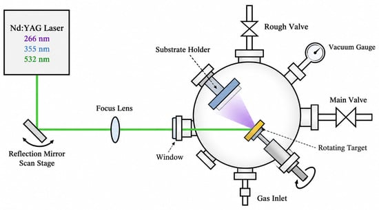
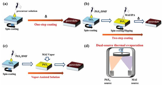
A PLD system comprises a pulsed laser, beam-delivery optics, a vacuum chamber, a target, and a temperature-controlled substrate. As illustrated in Figure 1, the laser beam is directed by a scanning mirror and focused onto a rotating target through an optical window, while the chamber pressure is monitored using a vacuum gauge and regulated through the gas inlet and vacuum control system. Above the ablation threshold, rapid heating, vaporization, and ionization generate a plume containing atoms, ions, molecules, clusters, and, under unstable ablation, particulates. Film formation can be viewed as three coupled stages: laser–target interaction, plume expansion and collision, and surface adsorption, diffusion, nucleation, and growth [6].
Figure 1.
Schematic illustration of a typical pulsed laser deposition (PLD) system. The green line represents the laser beam, while the purple region indicates the plasma plume. The black, blue, and green wavelength labels correspond to 266, 355, and 532 nm, respectively.
The first stage fixes the initial composition and energy distribution of the ejecta. Under an appropriate fluence regime, nonequilibrium ablation can enable near-stoichiometric transfer of complex targets, although volatile organic halides require compensation or alternative reaction pathways [21]. The ablated species generally expand preferentially along the target surface normal toward the substrate. During plume propagation, background gas and travel distance redistribute kinetic energy and species flux. The improvements in the composition and morphology of MAPbBr3 obtained by tuning laser fluence and Ar pressure illustrate how ablation and transport must be optimized together [22].
At the substrate, arrival flux and surface mobility govern nucleation density, texture, and defect formation. Increasing the deposition rate from 6 to 80 nm min−1 changed the preferred orientation of PLD-grown halide perovskite films and reduced carrier mobility [23]. Conversely, lattice matching enabled room-temperature epitaxy of α-MAPbI3 on KCl [24]. For CsPbBr3, substrate temperature strongly altered crystallization and carrier properties, with high crystallinity reported at 200 °C [25]. These examples show that energetic delivery is useful only when matched to the surface-kinetic window of the specific material.
PLD growth is therefore controlled by a cascade rather than by a single parameter: target ablation defines the source flux, plume collisions reshape that flux, and the substrate converts it into a microstructure. Section 2.3 considers the principal control variables within this coupled framework.
2.3. Process Parameters Governing Film Growth
Laser fluence and repetition rate, background pressure, substrate temperature, target-to-substrate distance, and target microstructure jointly determine the composition and structure of PLD films. As illustrated in Figure 1, laser fluence affects the laser–target interaction and ablation process, while background gas pressure and target-to-substrate distance influence the transport of ablated species toward the substrate. Background gas pressure affects the collision frequency of plume species, whereas the propagation distance influences their cumulative collisions and energy dissipation, thereby modifying angular spread, arrival energy, deposition rate, and compositional transfer [21]. These variables are strongly interdependent; a process window established for one target or chamber geometry cannot be transferred uncritically to another.
Laser fluence primarily controls the ablation regime, whereas repetition rate sets the time-averaged material flux and thermal load. Sub-threshold or marginal fluence produces unstable transfer; excessive fluence increases energetic species and particulate ejection. The rate-dependent loss of texture and mobility reported by Kliner et al. illustrates the trade-off between throughput and film quality [23]. A separate Al/TiO2 study also linked laser power and repetition rate to crystallinity, optical response, and morphology [26]; although not perovskite-specific, it provides a useful process-level example of this coupling. Representative studies of halide perovskites further illustrate the relationships between laser fluence, compositional transfer, and phase formation, as summarized in Table 1.
Table 1.
Laser fluence, composition, and phases of PLD-grown halide perovskites.
The results summarized in Table 1 indicate that laser fluence can influence film composition and phase formation, although phase identification alone does not directly quantify stoichiometry. Since target composition and deposition atmosphere also affect film growth, these observations should not be attributed to laser fluence alone, particularly when multiple parameters are varied simultaneously [22].
Background pressure controls plume collisions, while substrate temperature regulates surface diffusion, desorption, and phase selection. Representative substrate-temperature conditions and their effects on different halide perovskite compositions are summarized in Table 2.
Table 2.
Substrate-temperature effects in PLD-grown halide perovskites.
As shown in Table 2, elevated substrate temperatures improve crystallinity in certain inorganic perovskites, such as CsPbBr3 and Cs2AgBiBr6, whereas MAPbI3 and CsSnI3 can be deposited at room temperature. Mixed-halide perovskites have also been prepared at 100 °C, although this does not establish an optimal growth temperature. These results indicate that the appropriate thermal window depends on material composition, substrate properties, and deposition conditions.
Target density and microstructure determine how uniformly energy is absorbed and how material is ejected. Melt quenching densified CsPbBr3 targets, suppressed coarse particulates and high-energy species, and reduced deep-level defects in the resulting films [16]. During prolonged PLD runs, repeated laser irradiation may preferentially deplete volatile constituents from the target surface, potentially altering the plume composition and causing compositional drift in deposited films. Hoffmann-Urlaub et al. observed local organic depletion and SnI2-rich features on laser-irradiated tin-based perovskite targets [27]. However, Rodkey et al. reported no detectable change in the overall composition of Cs2AgBiBr6 targets after ablation [29], indicating that target evolution is material- and process-dependent. Target scanning and periodic surface renewal, as demonstrated in previous studies [7,29], can help improve deposition reproducibility. At the opposite end of the process chain, room-temperature PLD of SnO2 on 4-inch substrates demonstrated that plume control can support low-damage, wafer-scale processing [31].
Deposition rate and film thickness must be optimized together with defect-related losses and photovoltaic performance. Kliner et al. increased the deposition rate of MA1−xFAxPbI3 films from 6 to 80 nm min−1, but faster growth reduced preferential orientation and carrier mobility and was associated with lower photovoltaic performance [23]. Film thickness introduces a further trade-off between sufficient light absorption or layer coverage and efficient charge extraction. For CsPbBr3 solar cells, optimizing both the absorber and mesoporous TiO2 thicknesses to approximately 200 nm yielded a power conversion efficiency (PCE) of 6.3% [11]. Similarly, an approximately 40 nm PLD-NiOx layer, combined with optimized annealing, enabled a PCE of 5.47% [15]. Separately, melt-quenched CsPbBr3 targets suppressed deep-level defects and enabled a PCE of 10.71% [16]. These findings highlight the need to balance deposition throughput, film thickness, defect-related recombination, and device efficiency rather than optimizing individual parameters in isolation.
A useful process map must therefore connect target state and laser conditions to plume composition and energy, and then to nucleation, defects, and interface quality. Optimizing variables in isolation can merely move the limiting step; reproducible device fabrication instead requires material- and layer-specific windows defined by coupled structural, compositional, and electrical metrics.
3. Halide Perovskites and Solar Cell Architectures
3.1. Crystal Structure and Optoelectronic Properties
Halide perovskites generally adopt an ABX3 structure, where A represents a monovalent cation (e.g., MA+, FA+, or Cs+), B represents a divalent metal cation (e.g., Pb2+ or Sn2+), and X represents a halide anion (I−, Br−, or Cl−) [32,33]. Substitution across the three lattice sites tunes symmetry, bandgap, and carrier energetics. MAPbI3 combines strong absorption, low exciton binding energy, and long carrier-diffusion lengths [34,35,36,37], whereas the fully inorganic composition CsPbBr3 offers greater thermal robustness [38]. Halide alloying widens the accessible bandgap range but can introduce phase segregation and nanoscale compositional heterogeneity [39,40,41]. This chemical flexibility is therefore inseparable from stringent control of composition and defects. In PLD, the target and ablation regime add another level of control—and another potential source of nonuniformity—to the perovskite energy landscape [16].
3.2. Thin-Film Fabrication Routes
Perovskite-film crystallinity and uniformity govern charge transport, while scale-up magnifies small variations in nucleation and drying [42]. Solution and vapor-phase methods define the principal fabrication routes [43]. Solution processing remains prevalent because of its simplicity and low equipment burden. One-step deposition casts all precursors together; two-step processing first forms an inorganic layer, commonly PbI2, and then converts it with an organic halide [4,44]. Both routes have been extended to modules [45], but reproducibility depends on precursor chemistry, atmosphere, coating hydrodynamics, and solvent removal.
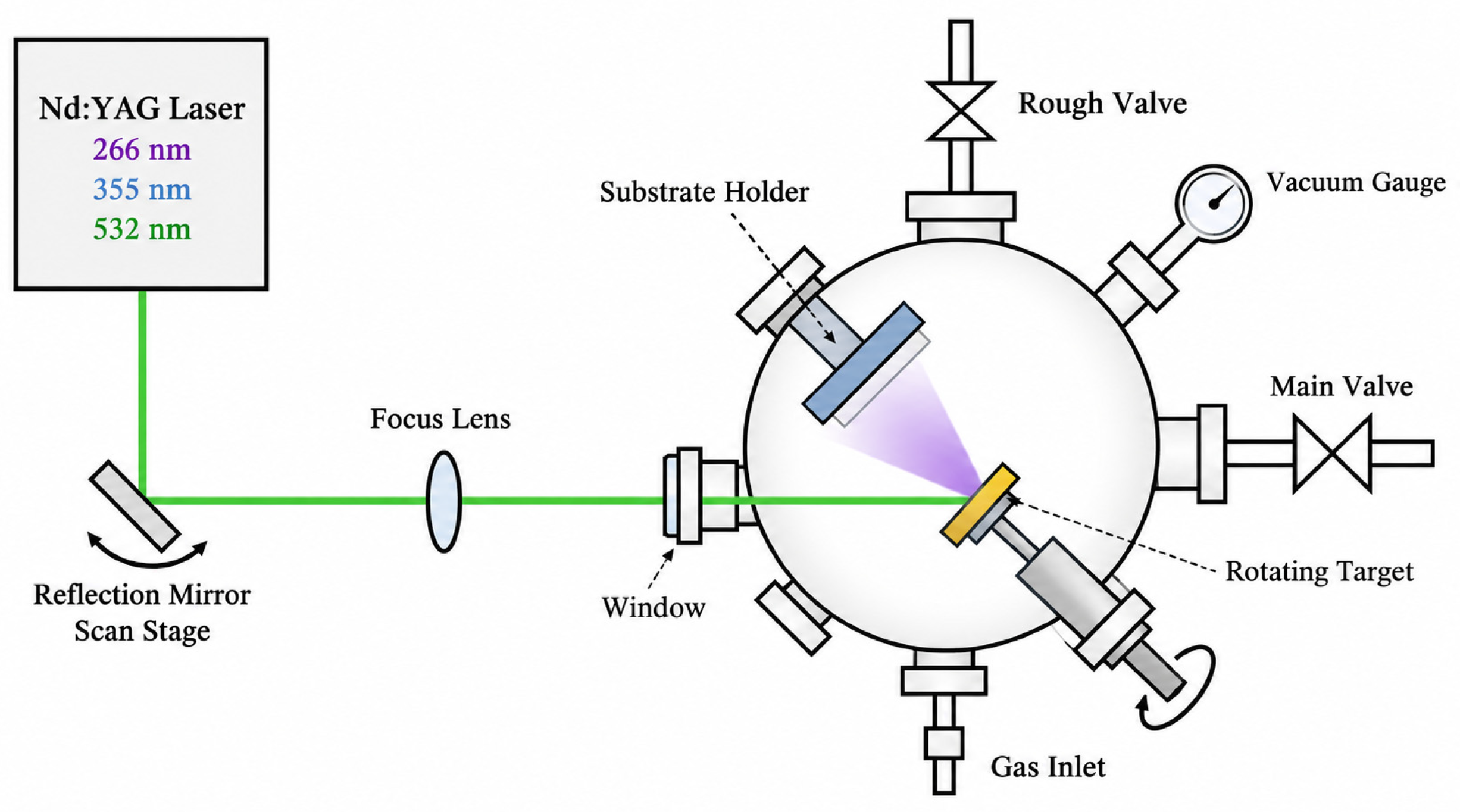
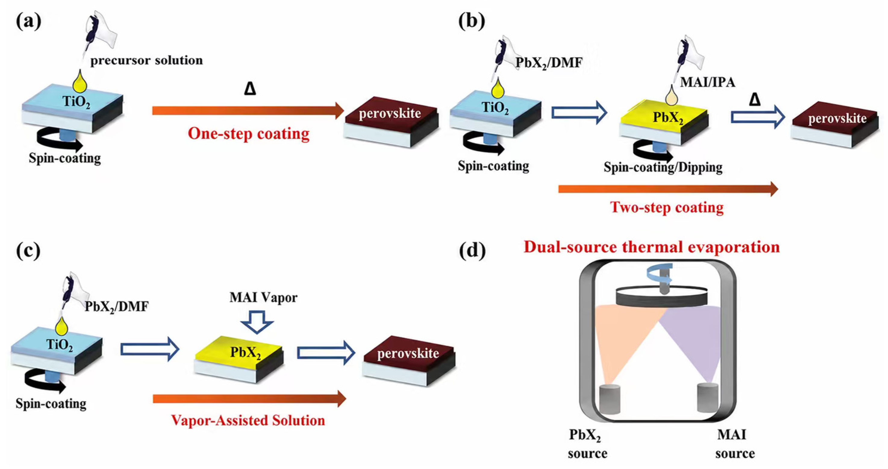
Vapor-phase methods remove the solvent variable and offer accurate thickness control, reproducible multilayers, and a plausible route to continuous manufacturing [46]. Dual-source co-evaporation, vapor-assisted conversion, and sequential evaporation have each produced perovskite films and devices [5,47,48]. Figure 2 compares representative solution and vapor routes.
Figure 2.
Representative fabrication routes for perovskite films: (a) one-step spin coating; (b) two-step sequential deposition; (c) vapor-assisted solution processing; and (d) dual-source thermal evaporation. The symbol ∆ indicates heating. Adapted from Ref. [49] under CC BY 4.0.
For mixed-cation and mixed-halide compositions, unequal component volatilities make vapor-flux control and stoichiometric closure particularly demanding [50]. PLD broadens the vacuum-processing toolbox beyond the absorber: ETLs and transparent conductors have been deposited by the same technique [12,19,51], including conductive films on 4-inch substrates [19].
Beyond these qualitative distinctions, reported photovoltaic metrics provide a quantitative perspective on the perovskite absorber-deposition methods discussed above. Single-source PLD of Cl-passivated MA1−xFAxPbI3 absorbers, combined with two-dimensional (2D) surface passivation, has achieved a solar-cell PCE of 19.7% [52]. By comparison, a 2025 review summarized reported cell efficiencies of 26.7% for spin coating, 25.31% for blade coating, 24.1% for slot-die coating, and 26.21% for sequential vacuum evaporation. Blade coating and slot-die coating have also demonstrated module efficiencies of 23.3% and 21.9%, respectively [53]. Regarding deposition rate, PLD growth of mixed-cation perovskites has been demonstrated at 6–80 nm min−1, although higher rates adversely affected film orientation and carrier mobility [23]. Despite its advantages in solvent-free processing and thickness control, PLD still faces challenges in deposition throughput and large-area uniformity. Importantly, these efficiency benchmarks originate from studies involving different absorber compositions, device architectures, and active areas, and therefore should not be interpreted as a direct ranking of deposition techniques.
3.3. Device Architectures and Operating Principles
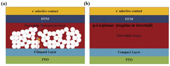
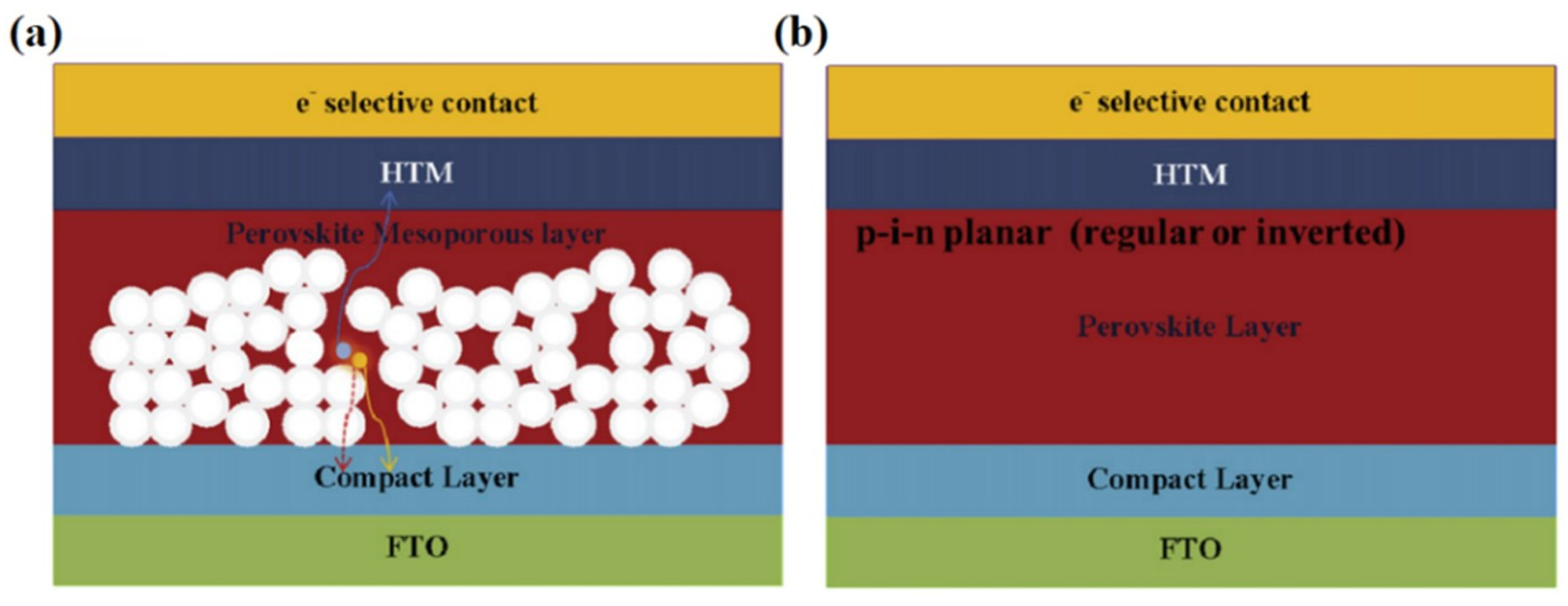
A PSC generally contains a transparent electrode, an electron-selective contact, the perovskite absorber, a hole-selective contact, and a counterelectrode. The polarity sequence defines conventional n–i–p and inverted p–i–n configurations. Independently, the absorber geometry can be mesoscopic or planar; Figure 3 compares these two structural classes. In both cases, contact selectivity and buried-interface quality control extraction, recombination, and stability. Improvements at the SnO2/perovskite interface and at the HTL/rear-electrode side have accordingly translated into better device performance [54,55].
Figure 3.
Representative perovskite solar cell (PSC) geometries: (a) mesoscopic and (b) planar architectures. Reprinted from Ref. [56] under CC BY 3.0.
Upon illumination, the absorber generates electrons and holes that are selectively extracted through the ETL and HTL. Bulk and interfacial defects introduce nonradiative recombination, whereas favorable band alignment and chemical passivation reduce voltage and collection losses [57,58]. Beyond these effects, recent impedance modeling has identified mobile-ion-induced charge-collection losses as an additional mechanism of performance degradation in perovskite solar cells [59]. PLD can tune thickness, coverage, defect chemistry, and interfacial damage in individual layers, making these properties the relevant link between deposition parameters and the short-circuit current density (JSC), open-circuit voltage (VOC), fill factor (FF), and PCE.
4. PLD Engineering of Perovskite Solar Cell Components
4.1. Hybrid Perovskite Absorbers
Hybrid perovskites combine volatile organic halides with less volatile metal-halide components, so stable compositional transfer is their defining PLD challenge. Bansode et al. used off-axis PLD at room temperature and compensated organic-species loss by enriching the target, yielding devices with a PCE of ≈7.7% [8]. A subsequent on-axis study combined nonstoichiometric targets with an Ar/H2 atmosphere and raised the PCE to 10.9% [9]. The comparison shows that target formulation and plume transport must be engineered together; nominal target stoichiometry alone does not guarantee film stoichiometry.
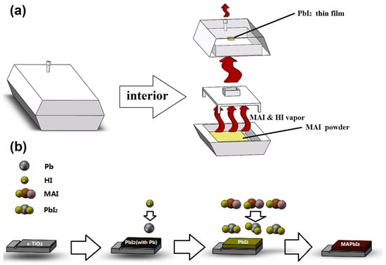
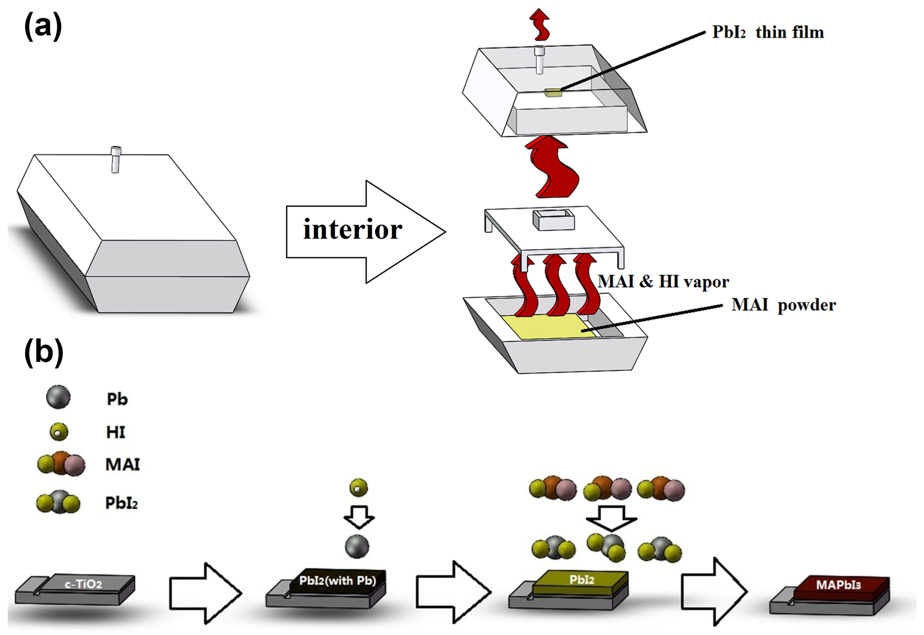
A second route separates inorganic deposition from organic incorporation. Zhang et al. deposited PbI2 by PLD and converted it to MAPbI3 by annealing in MAI vapor [10]. Conversion was incomplete at low reaction temperature, improved as grain growth accelerated, and gave way to MAPbI3 decomposition when the temperature became excessive. The process therefore trades single-step simplicity for independent control of precursor morphology and conversion chemistry. Figure 4 summarizes the configuration and reaction pathway.
Figure 4.
PLD-assisted formation of MAPbI3: (a) conversion of a PLD-deposited PbI2 precursor in methylammonium iodide (MAI) vapor and (b) the corresponding reaction pathway. Adapted from Ref. [10] under CC BY 4.0.
Single-source PLD has since been extended to mixed-cation absorbers. Soto-Montero et al. ablated a target containing MAI, formamidinium iodide (FAI), and PbI2 to deposit MA1−xFAxPbI3 in one step, producing devices with ≈14% PCE [7]. Excess organic halides in the target compensated for preferential loss of MAI and FAI, while fluence, pressure, and geometry provided further leverage over phase formation and composition. The result is best understood as engineered, rather than intrinsically stoichiometric, transfer.
Although single-target PLD simplifies the deposition process, large differences in constituent volatility and thermal stability can complicate stoichiometric transfer, particularly in hybrid halide perovskites [50]. For example, Bansode et al. obtained near-stoichiometric MAPbI3 films using MAI-enriched targets and off-axis deposition [8]. The challenge of compositional control also extends to inorganic perovskites: Cesaria et al. reported Br-deficient and Pb-enriched CsPbBr3 films, with compositional deviations influenced by target composition and the mass-dependent distribution of species in the plasma plume [28]. Unlike multi-source deposition, single-target PLD does not allow independent adjustment of constituent fluxes during growth, making compensation for preferential losses dependent on target composition and coupled deposition parameters. Sequential deposition of separate precursor layers followed by solid-state conversion, as demonstrated for CsPbIxBr3−x [60], offers an alternative approach to compositional control, although it requires additional processing steps.
More recent strategies combine composition control with passivation and directed nucleation. Incorporating PbCl2 into a single-source target for bulk passivation and applying oleylammonium iodide (OAmI) at the surface produced p–i–n devices with 19.7% PCE [52]. PbI2/CsxFA1−xPbI3 templates subsequently enabled uniform photoactive films on planar and textured substrates, with PCEs above 12.9% [61]. Hybrid-perovskite PLD has thus advanced from volatile-species compensation to deliberate control of nucleation and defect chemistry, although compositional closure remains the prerequisite for every downstream improvement.
4.2. All-Inorganic Perovskite Absorbers
Removing MA+ and FA+ avoids the most volatile organic constituents and generally improves thermal stability. CsPbBr3 is consequently the most developed all-inorganic absorber in PLD photovoltaics. Pulse number, substrate temperature, target composition, and target density have been used to tune thickness, crystallinity, and defect populations; related work has expanded to mixed-halide, lead-free, doped, and epitaxial perovskites.
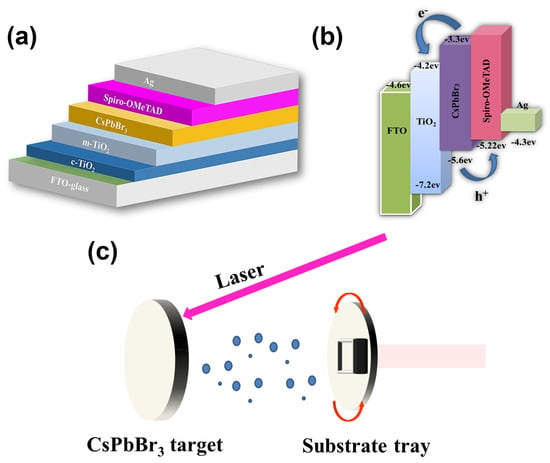
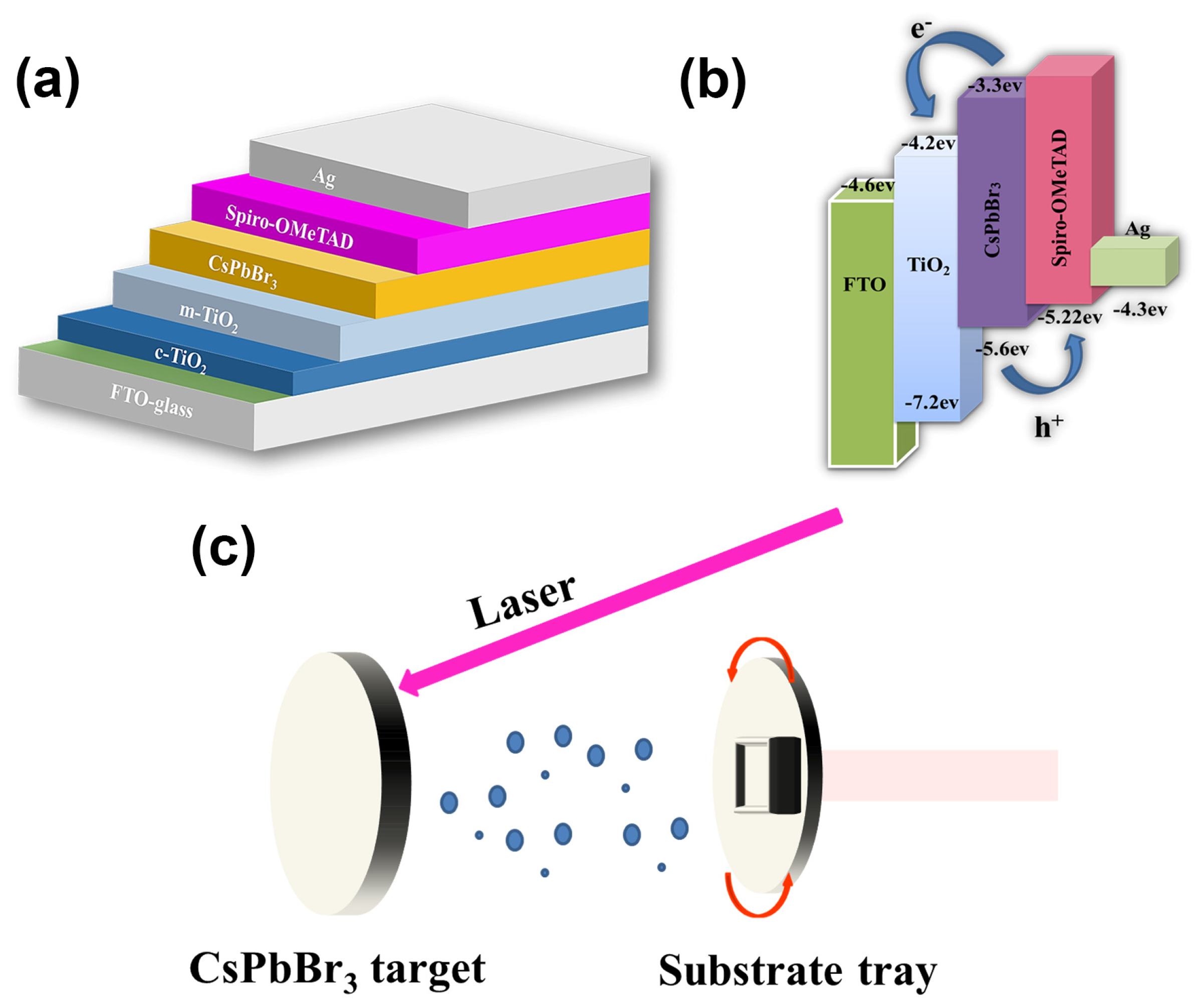
In 2019, Wang et al. prepared CsPbBr3 targets from single-crystalline powders and deposited compact CsPbBr3 thin films via PLD as an alternative to conventional solution-processing methods [11]. Specifically, single-crystalline CsPbBr3 powders were first grown by inverse temperature crystallization and subsequently pressed into solid targets. The resulting CsPbBr3 solar cell structure is illustrated in Figure 5a, while Figure 5b shows the corresponding energy-level alignment and charge-transfer pathways. As shown in Figure 5c, a focused pulsed laser ablates the CsPbBr3 target, generating a plasma plume that deposits CsPbBr3 onto the substrate and penetrates the mesoporous TiO2 layer. Ultimately, a maximum PCE of 6.3% was achieved when both the CsPbBr3 layer and mesoporous TiO2 scaffold were approximately 200 nm thick. The PLD-grown CsPbBr3 films also exhibited good stability under high-humidity conditions, highlighting the importance of thickness optimization and film quality.
Figure 5.
PLD of CsPbBr3 thin films: (a) the device structure; (b) energy-level alignment and charge-transfer pathways; and (c) deposition scheme. The blue circles in (c) represent laser-ablated species traveling from the CsPbBr3 target toward the substrate. Reprinted with permission from Ref. [11]. 2019, ACS.
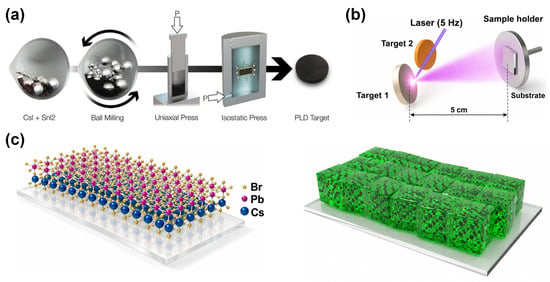
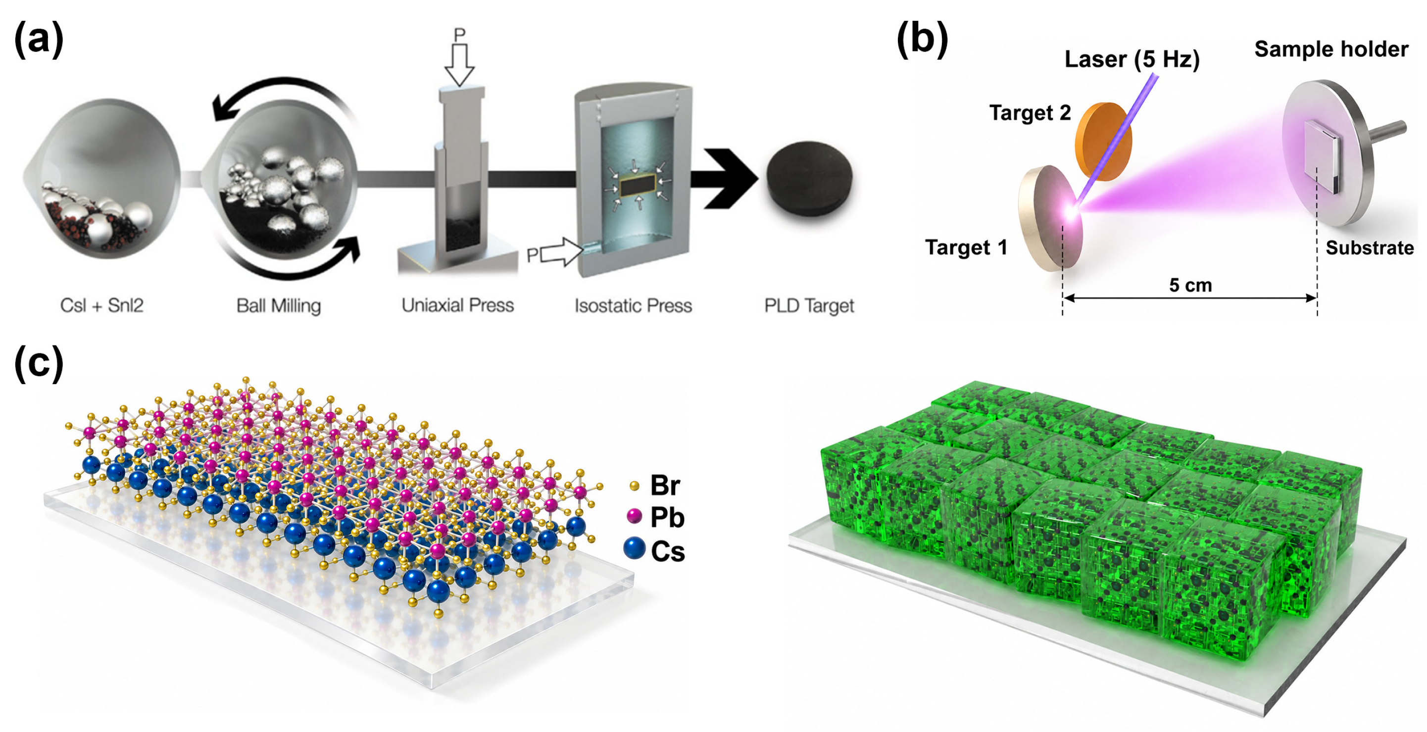
Kiyek et al. used ball milling to homogenize stoichiometric CsI and SnI2 powders, followed by isostatic pressing to obtain compact targets with densities exceeding 85% of the calculated value. Notably, the target retained the precursor phases, whereas black γ-CsSnI3 formed during room-temperature PLD (Figure 6a) [30]. In contrast, Rodkey et al. employed mechanochemical ball milling to synthesize nearly phase-pure Cs2AgBiBr6 powders, which were subsequently pressed into solid targets without loss of phase purity. PLD at a substrate temperature of 200 °C produced crystalline films with grain sizes of 200–300 nm [29]. Based on the single-source deposition, Jin et al. developed the double-source preparation of CsPbIxBr3−x thin films via PLD in the same year. Initially, bare CsBr, CsI, PbI2 and PbBr2 targets are produced by high-pressure pressing of their powders, respectively. Then as demonstrated in Figure 6b, two corresponding CsX and PbY2 (X, Y = Br, I) targets were successively chosen for PLD to deposit CsX and PbY2 thin films as two solid precursors on the same substrates in vacuum, followed by a high-temperature solid-state reaction into CsPbIxBr3−x, with precursor thickness controlling halide content and grain size [60]. Figure 6c further illustrates the resulting perovskite crystal structure and patterned thin-film morphology.
Figure 6.
Schematic illustration of (a) the preparation of a CsSnI3 PLD target via ball milling and pressing. Reprinted from Ref. [30] under CC BY 4.0. (b) Double-source PLD of precursor layers; and (c) the resulting perovskite crystal structure and patterned thin-film morphology. Reprinted with permission from Ref. [60]. 2021, Wiley-VCH GmbH.
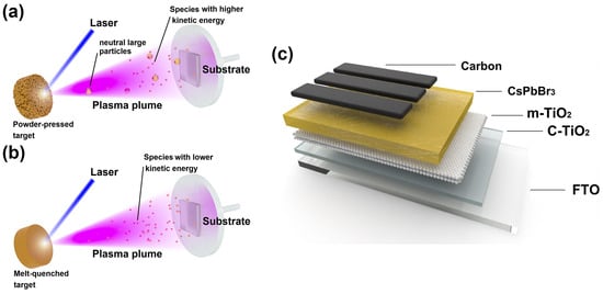
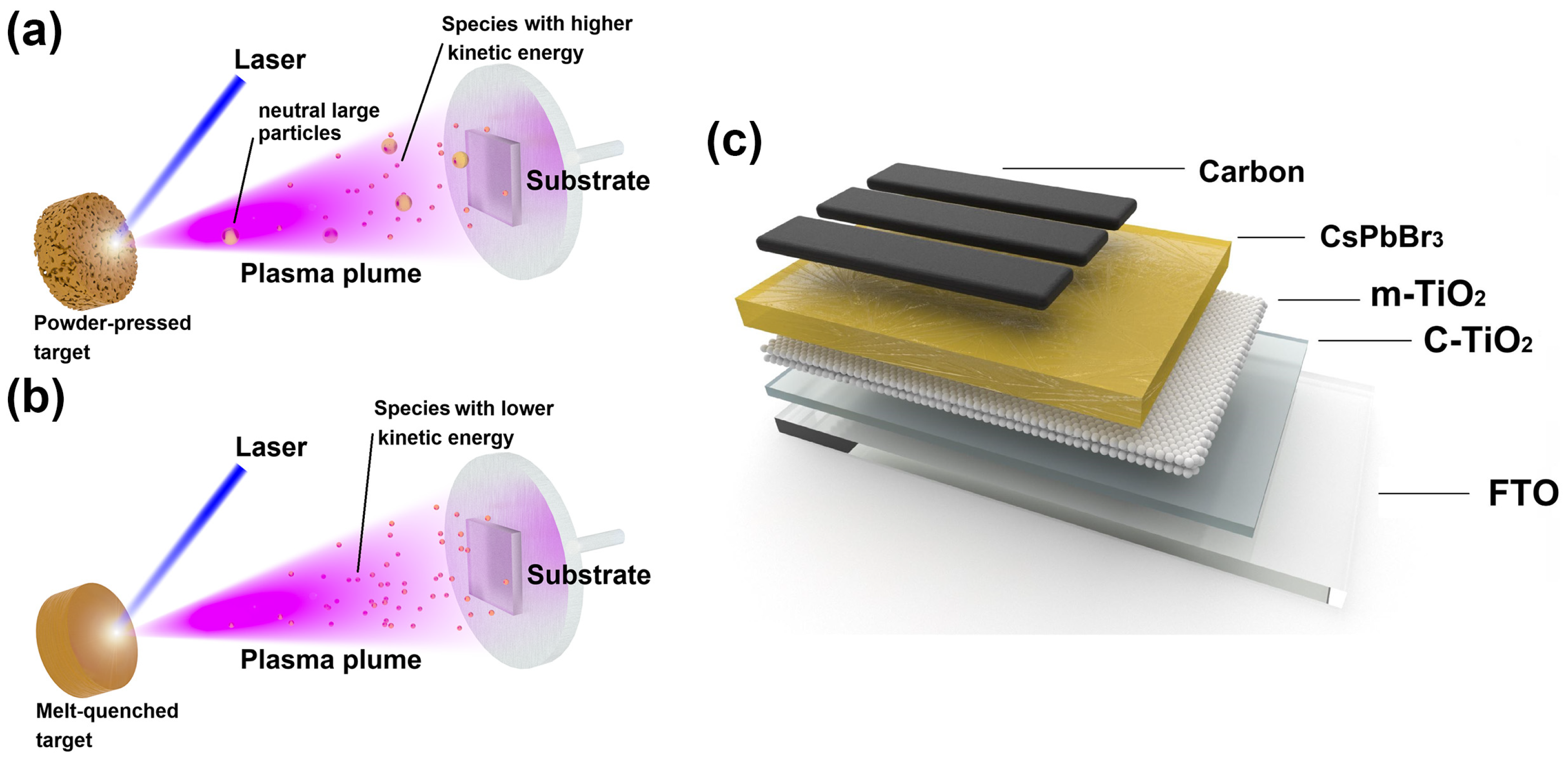
Target engineering has delivered the clearest recent improvement. Conventional powder-pressed CsPbBr3 targets contain pores that destabilize local heating, eject coarse neutral particulates, and increase plume-species energy. Therefore, Fan et al. developed a melt-quenched method to improve these drawbacks above [16]. Compared with conventional powder-pressed targets shown in Figure 7a, melt-quenched targets possess a denser microstructure with fewer internal voids and improved thermal conductivity, thereby suppressing the emission of large neutral particles and droplets from the target surface and reducing the average kinetic energy of species in the plasma plume (Figure 7b). Consequently, devices (Figure 7c) fabricated using melt-quenched targets achieved a PCE of 10.71%, and unencapsulated cells retained 93% of their initial efficiency after 150 days of storage at room temperature and 70% relative humidity [16].
Figure 7.
Effect of CsPbBr3 target microstructure on ablation and particle transport: (a) a powder-pressed target emits more coarse particulates and energetic species; (b) a melt-quenched target suppresses large-particle ejection and lowers plume-species energy; (c) schematic of FTO/c-TiO2/m-TiO2/CsPbBr3/Carbon structured PSCs. Reprinted with permission from Ref. [16]. 2026, Wiley-VCH GmbH.
These studies illustrate the distinct but sometimes complementary roles of powder pressing, ball milling, and melt quenching in PLD target preparation. Pressing primarily consolidates precursor powders, whereas ball milling can either improve compositional homogeneity without forming the final perovskite phase [30] or induce mechanochemical synthesis before target consolidation [29]. For CsPbBr3, Fan et al. reported that melt-quenched targets exhibited a 14.1% higher density than conventional powder-pressed targets, accompanied by reduced emission of large particles and lower kinetic energies of ablated species [16]. Thus, target preparation influences density, phase constitution, and ablation behavior through different mechanisms. However, a quantitative ranking of all three approaches remains premature because the available studies involve different material compositions and processing conditions.
Materials-oriented studies point to further design space. Eu3+-doped CsPbBr3 was grown epitaxially on SrTiO3, with doping altering carrier type, defects, and electrical response [62]. In a separate photodetector study, Ag nanoislands coupled to CsPbBr3 made by a PLD-assisted solid-state reaction enhanced absorption through localized surface plasmons and extended the response through hot-electron injection [63]. These are not photovoltaic demonstrations, but they establish capabilities—dopant incorporation and heterostructure assembly—that could be translated to solar-cell interfaces.
All-inorganic perovskite PLD has consequently moved beyond thickness optimization toward control of complex compositions, target microstructure, dopants, and heterointerfaces. The evidence consistently identifies target quality and ablation stability as upstream determinants of crystallization and deep-defect formation. Reproducible targets and robust process windows are therefore likely to yield larger gains than further isolated optimization of pulse count or temperature.
4.3. Electron-Transport Layers
An ETL is used to extract electrons, block holes, and form a chemically and electronically benign contact with the absorber. Its thickness, conductivity, defect chemistry, and band alignment determine transport and recombination losses. TiO2, SnO2, and ZnO are natural PLD targets because their oxygen stoichiometry and dopant profiles can be adjusted through deposition atmosphere and target composition. The field has advanced from simple thickness optimization to nanoscale transport mapping, gradient doping, and low-damage scale-up.
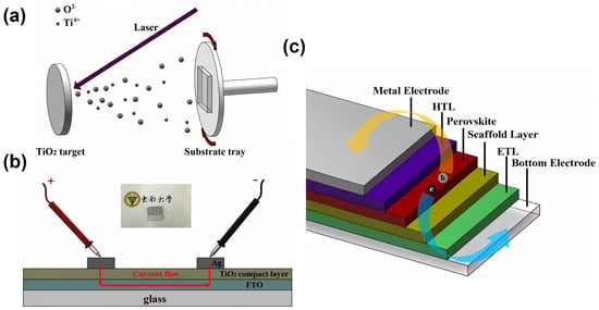
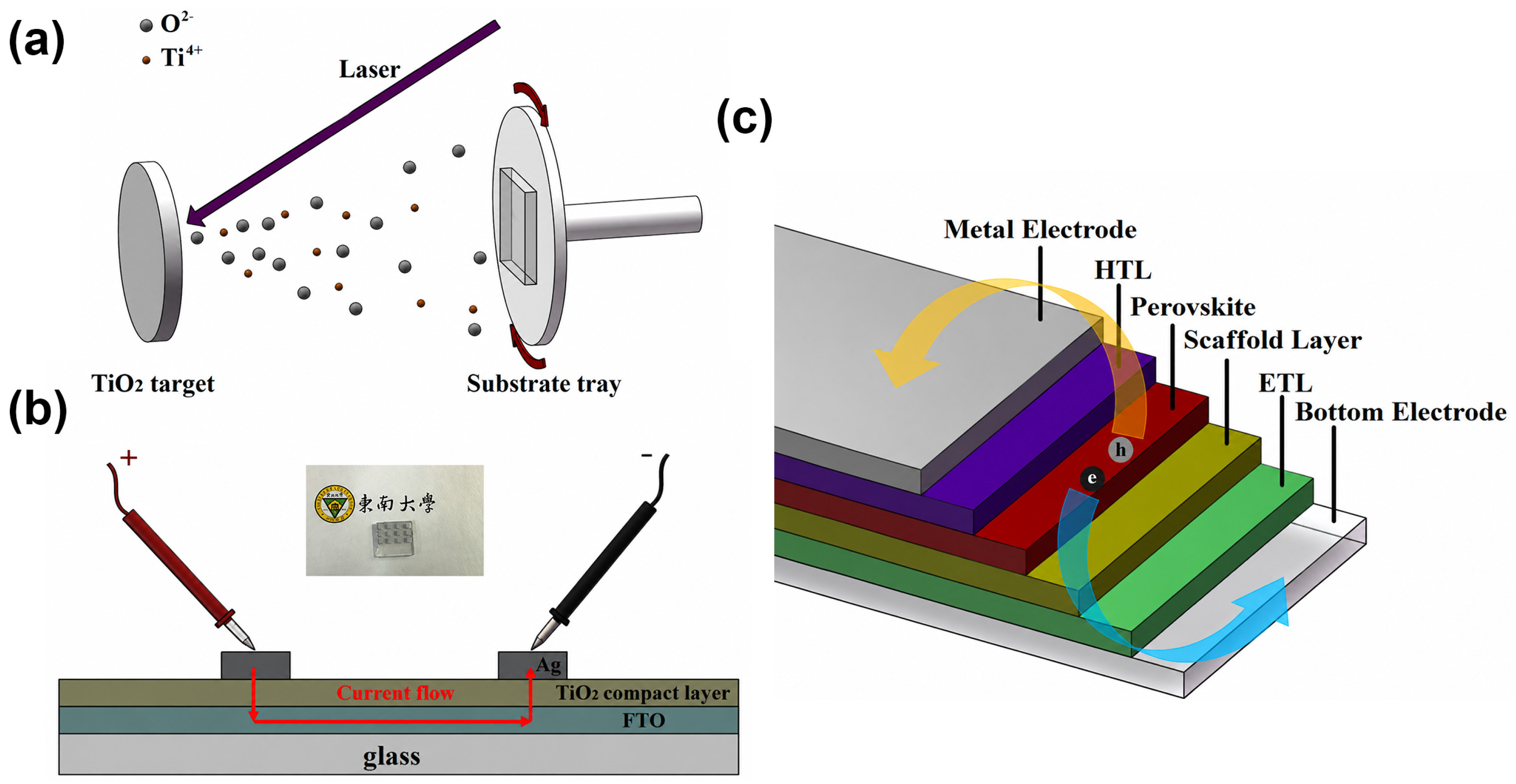
Similarly, TiO2 thin films can be prepared by the deposition of a plasma composed of Ti4+ and O2− on substrates, as shown in Figure 8a. In comparison with the common spin coating method, TiO2 layers prepared by PLD are more compact, leading to a more uniform coverage of the interface. Figure 8b is the schematic of compactness assessment of TiO2 layers where at the same thickness higher resistance corresponds to more compact performance. In comparison, PLD-prepared TiO2 thin films show two magnitudes larger than those prepared by spin coating. Ref. [12] Finally, Zhang et al. obtained a maximum PCE of 13.95% in MAPbI3 PSCs with a 32 nm thick compact TiO2 layer (Figure 8c). Post-deposition annealing reduced oxygen-vacancy density and improved transparency and electron transport, while PLD produced compact, pinhole-poor layers.
Figure 8.
PLD TiO2 electron-transport layers (ETLs): (a) deposition of a compact TiO2 layer; (b) compactness assessment; and (c) integration of the PLD-TiO2 layer in a PSC. The arrows in panels (a–c) indicate the laser incidence and substrate rotation, current flow, and charge-transport pathways, respectively. The Chinese text in the inset of panel (b) refers to Southeast University. Reprinted with permission from Ref. [12]. 2018, WILEY-VCH Verlag GmbH & Co. KGaA, Weinheim, Germany.
Local conduction can be as important as average film conductivity. Conductive atomic force microscopy revealed one-dimensional transport pathways in optimized PLD-TiO2, which correlated with device efficiencies of ≈17% [64]. Gradient N doping subsequently enabled simultaneous tuning of conductivity and band alignment across TiO2:N, creating a cascade energy landscape. With the additional incorporation of an MgF2 antireflective layer and a 2D perovskite passivation layer, the graded-TiO2:N-based n–i–p devices achieved a champion reverse-scan PCE of 22.98% and a forward-scan PCE of 21.27% [65]. Reporting both scans is important because the difference indicates residual hysteresis despite the high peak value.
SnOx provides a representative example of atmosphere-mediated defect engineering. Industrial-scale PLD at low chamber pressure produced smooth and pinhole-poor oxide thin films because low oxygen pressures can reduce collisions between laser-ablated species and gas molecules. In contrast, an O2-rich atmosphere can suppress the formation of oxygen vacancies, thereby modifying the carrier concentration, electrical conductivity, and interfacial charge transport characteristics. After balancing morphology and oxidation state, n–i–p devices exceeded 18% PCE [14].
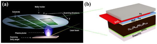
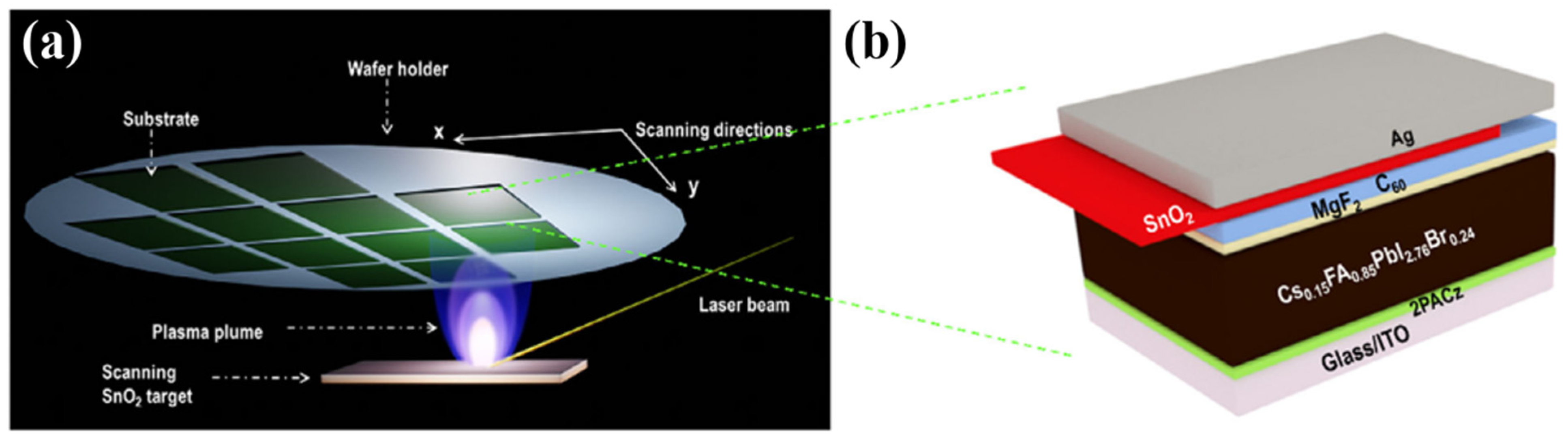
Soltanpoor et al. extended this concept to low-damage, wafer-scale processing by depositing SnO2 at room temperature onto C60 in p–i–n cells [31]. Thickness homogeneity exceeded 98.5% across ≈100 cm2, and devices reached 17.8% PCE. The combination of low temperature, solvent-free growth, and a thermalized plume protected the underlying organic layer while meeting a meaningful area-uniformity benchmark. Figure 9 shows the scanning configuration and device stack.
Figure 9.
Wafer-scale PLD of a SnO2 buffer layer: (a) 4-inch deposition and scanning configuration; and (b) p–i–n device architecture with SnO2 deposited on C60. Reprinted from Ref. [31] under CC BY 4.0.
PLD-ZnO provides a parallel route to morphology-guided transport. Nanoscale mapping associated improved device response with high local conductivity and vertically oriented conductive features [66]. Across TiO2, SnO2, and ZnO, the emerging design rule is consistent: film thickness and average composition are insufficient descriptors. Spatially resolved conductivity, oxygen-vacancy distribution, band offsets, and damage to the underlying contact must be optimized together.
4.4. Hole-Transport Layers
An HTL must selectively extract holes while suppressing electron leakage and interfacial recombination. NiOx is particularly attractive for PLD because it combines optical transparency and chemical stability with a tunable valence-band position. Annealing, target doping, thickness, oxygen pressure, and substrate temperature can all alter its carrier density, defect spectrum, and contact energetics.
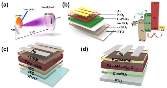
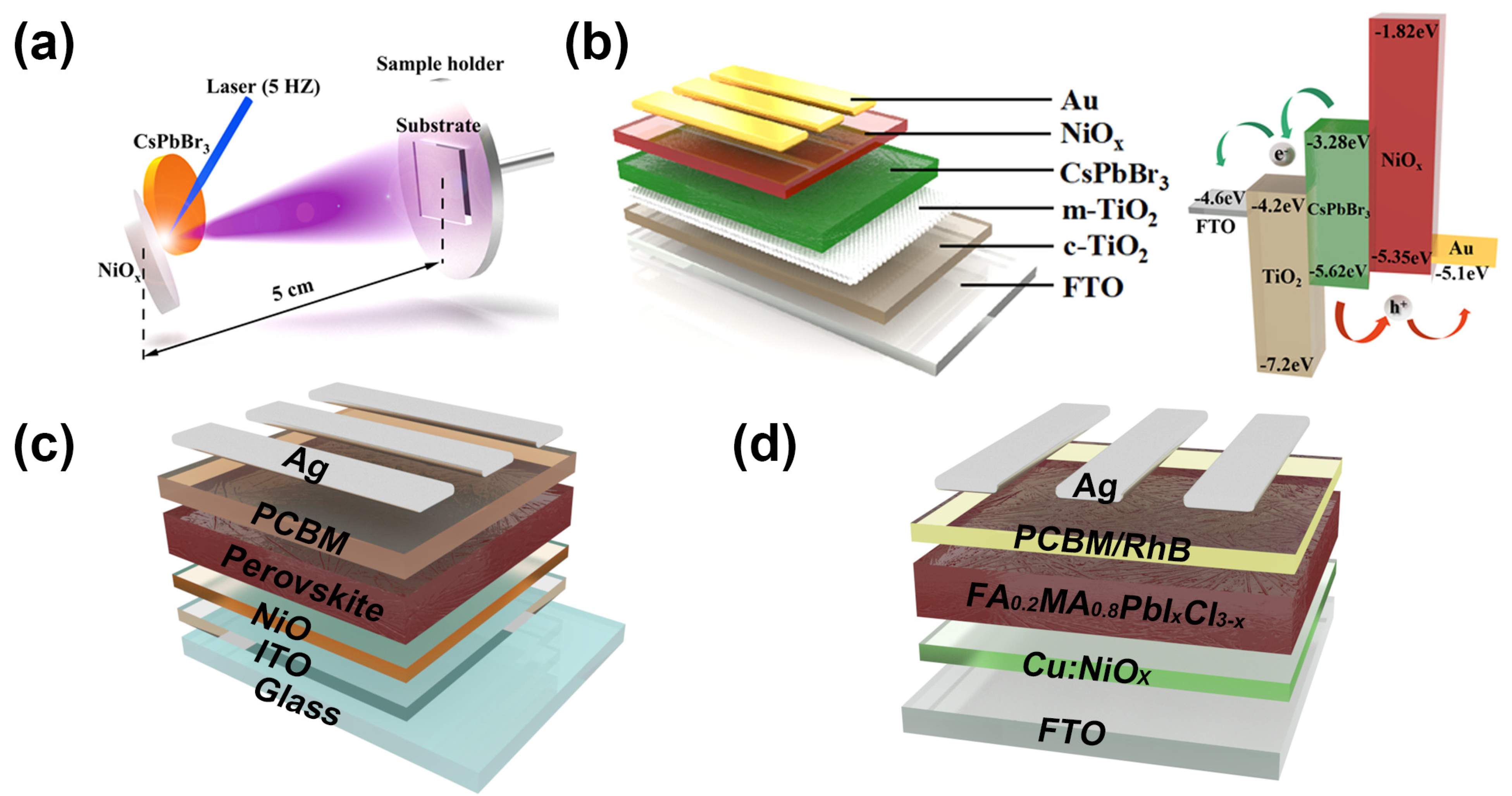
In 2023, Song et al. prepared CsPbBr3 solar cells in which both CsPbBr3 and NiOx layers were fabricated via PLD as shown in Figure 10a [15]. In their work, it is found that the thickness and thermal treatment of NiOx layers were critical for device performance, in which an ≈40 nm NiOx layer annealed at 250 °C achieved a highest PCE of 5.47% and retained 95% of their initial efficiency after 1200 h at 85 °C and 30% relative humidity without any encapsulation. The improved stability is mainly attributed to compact CsPbBr3 and NiOx thin films without any damage from solvent evaporation to the morphology and crystal quality. Figure 10b illustrates the structure and energy band diagram of the solar cells.
Figure 10.
(a) Fabrication schematic of both CsPbBr3 and NiOx layers via PLD; Schematic diagram of the device architecture in the work of (b) Song et al. Reprinted with permission from Ref. [15]. 2023, AIP Publishing. (c) Qiu et al. [13] and (d) Feng et al. [67].
Qiu et al. showed that annealing PLD-NiO improved crystallinity, transparency, and surface uniformity, raising PCE from 5.38% to 12.59%; Li doping through the target further increased conductivity and produced 15.51% PCE (Figure 10c). Ref. [13] Feng et al. used the same target-engineering principle with Cu: 3% Cu increased hole concentration and conductivity, yielding 20.41% PCE (Figure 10d). Ref. [67]. These studies establish doped targets as a direct route from ablation chemistry to transport-layer electronic structure.
Deposition conditions provide a second handle on intrinsic NiOx defects. Horynova et al. varied oxygen pressure, substrate temperature, and repetition rate and found that substrate temperature exerted the strongest influence on composition, optical response, defect states, and microstructure [68]. A moderate oxygen pressure reduced sub-bandgap absorption. The study reinforces the need to optimize electronic loss channels, rather than crystallinity alone, when defining an HTL process window.
PLD-NiOx engineering has thus progressed from annealing and thickness control to deliberate manipulation of extrinsic dopants and intrinsic defects. Because the same platform can deposit NiOx and selected perovskite absorbers, it also provides a practical test bed for sequential vacuum growth. The remaining challenge is to achieve the required conductivity and band alignment without imposing thermal or particle-energy conditions that damage adjacent layers.
4.5. Interfaces and Other Functional Layers
Buffer, protective, and transparent conducting layers determine whether the properties of the absorber and selective contacts survive device completion. PLD is useful here because thickness and plume energy can be adjusted independently over a broad range, enabling dense barriers or conductors to be deposited at low substrate temperature. The same energetic species that promote compact growth, however, can damage organic contacts, making kinetic-energy control central to interface engineering.
Room-temperature SnO2 deposition onto C60 exemplifies this balance. By increasing plume thermalization, Soltanpoor et al. formed a large-area oxide buffer without measurably compromising the underlying organic contact [31]. In this role, SnO2 is not simply an ETL; it is a protective layer that allows subsequent vacuum processing under a low thermal and mechanical damage budget.
PLD oxides can also provide spectral protection. Gibson et al. deposited TiO2, ZnO, and Al-doped ZnO at room temperature and tuned their optical gaps and ultraviolet (UV) absorption through oxygen partial pressure [69]. In TiO2, oxygen vacancies and Ti3+ states contributed to the observed bandgap changes. ZnO coatings reduced UV-induced degradation of MAPbI3, highlighting the potential of PLD-grown oxides as spectrally protective layers [69].
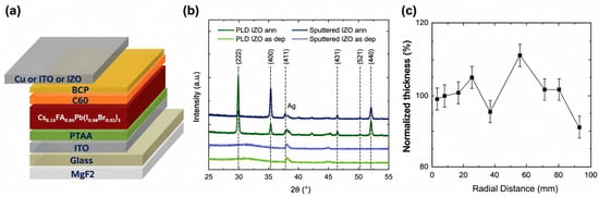
Transparent electrodes extend PLD to the final device contact. Smirnov et al. deposited Zr-doped In2O3 (IZrO) at room temperature on 4-inch substrates [19]. The as-grown films were predominantly amorphous and crystallized after annealing below 200 °C; thickness varied by only ±5.3% across the substrate. Integration as a transparent rear electrode in semitransparent PSCs demonstrated compatibility with sensitive underlying layers. Figure 11 connects the device architecture, structural evolution, and wafer-scale thickness profile.
Figure 11.
PLD-grown Zr-doped In2O3 (IZrO) transparent rear electrodes: (a) PSC architectures; (b) grazing-incidence X-ray diffraction patterns of PLD- and radio-frequency-sputtered IZrO before and after annealing; and (c) normalized thickness across a 4-inch substrate. Adapted from Ref. [19] under CC BY 4.0.
A subsequent study isolated deposition pressure as a control over ITO-induced interface damage [70]. Higher pressure increased gas-phase collisions and reduced the energy delivered to C60/bathocuproine, leading to higher VOC and FF in semitransparent cells. Excessive thermalization can, however, degrade conductivity or interfacial contact. Transparent-electrode integration therefore requires a three-way compromise among impact damage, optical transmission, and electrical resistance.
Evidence from sputtered transparent electrodes supports the same principle. Singha et al. inserted metal-oxide buffers to protect sensitive contacts during radio-frequency magnetron sputtering while retaining optical transmission and charge transport [71]. This was not a PLD study, but it clarifies the function that a PLD-grown buffer must perform before a more energetic electrode process.
These examples reposition PLD from an absorber-growth method to an interface-enabling technology. Pressure and geometry can reduce bombardment, while oxide composition and thickness set barrier quality, optical loss, and contact resistance. Such control is essential if sequential vacuum processing is to preserve rather than erase the gains made in earlier layers.
4.6. Multilayer Integration and Vacuum-Processed Devices
Applications to absorbers, transport layers, buffers, and transparent conductors establish the ingredients for sequential vacuum fabrication. Unlike wet coating, a vacuum step need not redissolve or swell an underlying layer, and it offers accurate thickness control across multilayer heterostructures [21]. Integration nevertheless succeeds only when the atmosphere, substrate temperature, and particle-energy window of each step is compatible with every layer already present.
Partial integration has already been demonstrated: CsPbBr3 and NiOx were both deposited by PLD [15], SnO2 was added as a low-damage buffer [31], and ITO was deposited as a transparent top electrode [20]. Most reports, however, use PLD for only one or two layers. They should therefore be described as PLD-enabled or PLD-integrated devices, not as fully PLD-fabricated solar cells.
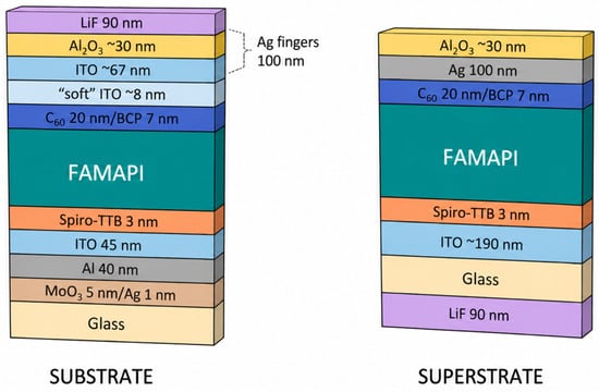
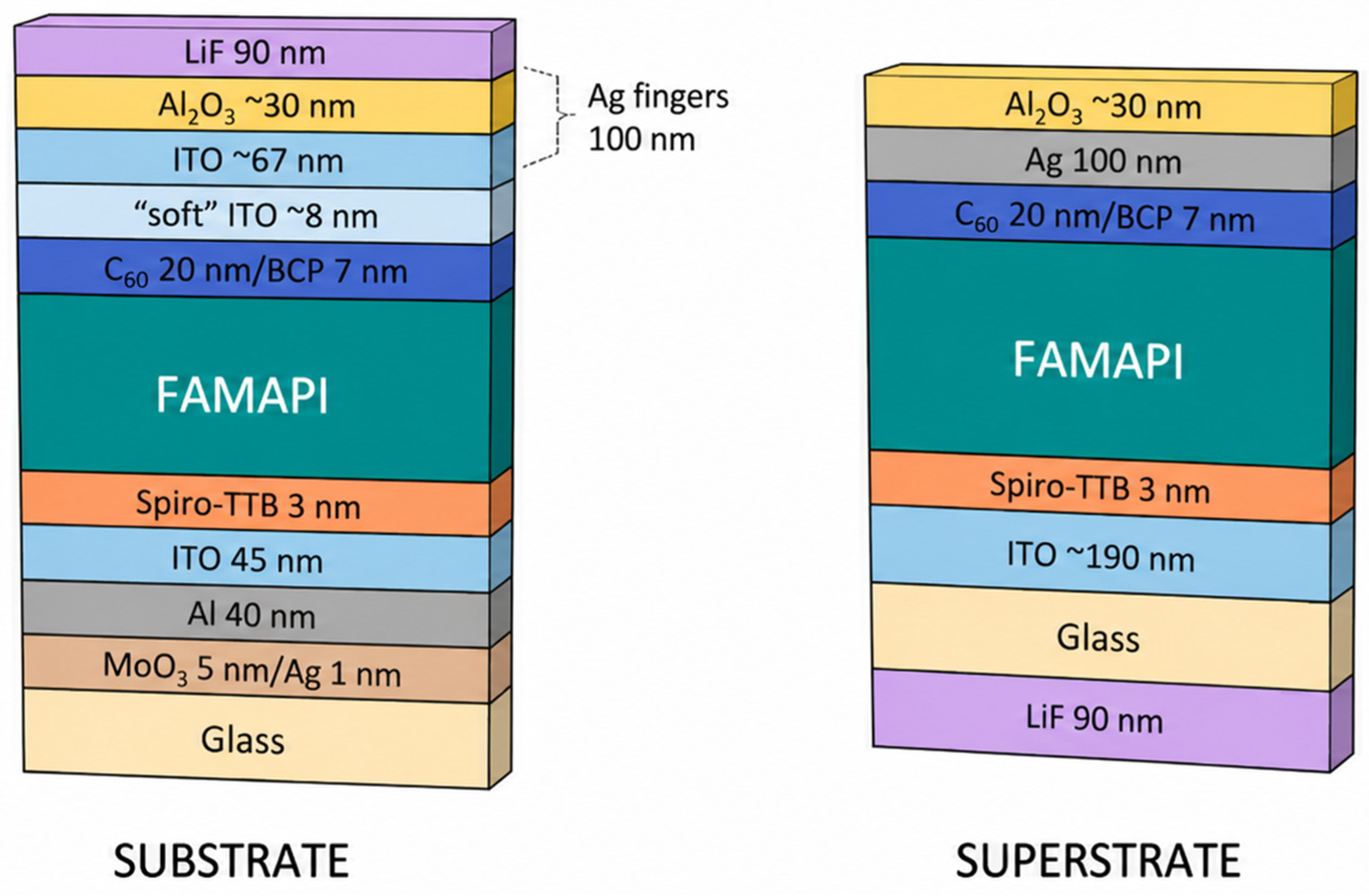
Paliwal et al. combined PLD transparent conductive oxides with thermally evaporated functional layers to realize fully vacuum-processed substrate and superstrate devices with ≈19% PCE [72]. Figure 12 illustrates the device architectures of the substrate and superstrate configurations. At the absorber level, single-source PLD with PbCl2 bulk passivation and oleylammonium iodide (OAmI) surface treatment reached 19.7% PCE [52], while templated PLD produced CsxFA1−xPbI3 on planar and textured substrates [61]. Collectively, these studies identify complementarity among vacuum methods—not exclusivity—as the practical route to complex stacks.
Figure 12.
Fully vacuum-processed PSCs incorporating PLD: substrate and superstrate device architectures [72].
Fully vacuum-processed PSCs now provide a demanding benchmark for this integration strategy. Choi et al. reported 23.2% PCE for an inverted cell and 12.3% for a 25 cm2 single cell [73]. Controlled solid-state crystallization subsequently produced 25.53% PCE [74]. For wide-bandgap absorbers, crystal-facet-directed vacuum growth delivered 19.3% laboratory efficiency and 18.35% certified efficiency; the corresponding all-vacuum monolithic perovskite/silicon tandem reached 24.3% [75]. These devices were not fabricated entirely by PLD, but they define the interfacial and crystallization control that any PLD-containing vacuum line must match.
The central integration problem for PLD is the mismatch among layer-specific windows for volatile-species retention, atmosphere, temperature, and bombardment energy. In situ photoluminescence has already been used during thermally evaporated perovskite growth to track nucleation and guide a structure-directing layer, enabling 23.3% PCE [76]. Although demonstrated outside PLD, the measurement concept is directly transferable: optical monitoring, plume diagnostics, and multi-target switching could provide closed-loop control as PLD is combined with evaporation and other vacuum methods.
PLD is therefore most compelling as a selective module within an integrated vacuum platform. Its strengths-rapid target exchange, compositionally complex oxides, pulse-resolved thickness control, and low-temperature dense-film growth—can be assigned to the layers that benefit most, while evaporation or other methods handle volatile absorbers and molecular contacts.
5. Challenges and Opportunities
PLD now addresses nearly every functional layer in a PSC, but five barriers separate isolated demonstrations from scalable manufacturing: compositional transfer in volatile absorbers, target reproducibility, particulate suppression, area uniformity and throughput, and compatibility across a multilayer sequence. Hybrid perovskites are especially demanding because their constituents differ sharply in vapor pressure and thermal stability. Compositionally enriched targets and single-source passivation have improved film quality [7,52], yet quantitative relationships among target depletion, plume composition, and accumulated film stoichiometry remain poorly standardized.
Target engineering is the most immediate opportunity. Porosity and spatially nonuniform heat flow in powder-pressed targets promote unstable ablation and coarse particulates, whereas melt-quenched dense targets reduce both deep traps and morphological defects [16]. Future studies should report target density, phase purity, surface evolution, and usable lifetime alongside film data. Time-resolved optical emission, mass-resolved plume diagnostics, and in situ film probes could then connect target aging to process drift. Vacuum-assisted processing studies have already demonstrated that in situ growth monitoring and crystallization control can broaden processing windows [77].
Scale-up introduces a distinct geometric constraint: the highly directional plume produces thickness and composition gradients unless the beam, target, or substrate is scanned. Although wafer-scale PLD of SnO2 buffer layers has achieved thickness homogeneity exceeding 98.5% across approximately 100 cm2 [31], this result does not establish comparable uniformity for halide perovskite absorbers. Jin et al. demonstrated the preparation of CsPbIxBr3−x films using PLD-deposited precursor layers followed by solid-state conversion [60], but this route is distinct from direct PLD growth of the complete perovskite absorber. Consequently, evidence for uniform, large-area halide perovskite absorber films grown directly by PLD, particularly those integrated into photovoltaic modules, remains limited. Vacuum quenching and hybrid solution–vacuum processing have enabled the fabrication of large-area perovskite modules [77,78,79], while high-rate vapor transport deposition and close-space sublimation have demonstrated complementary advances in deposition throughput and tandem-cell integration [80,81]. These approaches provide manufacturing benchmarks rather than direct evidence for PLD scalability. Within PLD, raising the rate from 6 to 80 nm min−1 reduced orientation and mobility [23]. Scale-up must therefore optimize throughput, utilization, and uniformity without sacrificing electronic quality.
Reported stability metrics for PLD-fabricated perovskite devices are not directly comparable because aging protocols differ across studies. For example, unencapsulated CsPbBr3 solar cells incorporating PLD-grown CsPbBr3 and NiOx retained 95% of their initial power conversion efficiency after 1200 h at 85 °C and 30% relative humidity [15], whereas unencapsulated devices fabricated using melt-quenched CsPbBr3 PLD targets retained 93% after 150 days of storage at room temperature and 70% relative humidity [16]. The former evaluates thermal stability under elevated-temperature exposure, while the latter reports ambient-storage durability; neither result alone establishes operational lifetime under continuous illumination and electrical bias. Reliable cross-study comparisons therefore require reporting the stress conditions, encapsulation status, aging duration, and measurement procedures, preferably following standardized testing and reporting protocols based on the International Summit on Organic Photovoltaic Stability (ISOS) guidelines [82].
Economics and environmental performance require equally careful treatment. Although PLD avoids processing solvents during film deposition, this benefit must be evaluated alongside the electricity required for laser operation and vacuum pumping [21,51]. Laser and vacuum equipment require substantial capital investment, while target preparation, system maintenance, deposition throughput, production yield, and equipment uptime influence operating costs. Material utilization is another concern, as not all ablated species reach the substrate, potentially increasing material losses. For lead-containing perovskites, spent targets and chamber residues also require appropriate collection and waste management. A recent life-cycle assessment of perovskite manufacturing suggests that larger production scales and improved process control can reduce environmental impacts per unit area, although these findings are not specific to PLD [83]. PLD assessments should consequently include energy consumption and manufacturing cost per unit coated area, target utilization, scanning efficiency, waste-management requirements, maintenance costs, deposition throughput, and production yield, rather than inferring manufacturability from deposition area alone.
The near-term opportunity is a hybrid vacuum line in which PLD is reserved for layers that benefit from energetic, composition-flexible growth. Fully vacuum-processed cells already obtain high efficiencies through passivation, controlled solid-state crystallization, and optimized deposition order [74,84,85]. Translating these advances to PLD-containing stacks will require standardized targets, closed-loop composition control, low-damage plume conditions, and compatible temperature and atmosphere windows. If these requirements are met, multi-target PLD could connect laboratory film design to continuous fabrication of robust multilayer photovoltaics.
6. Conclusions
PLD has progressed from a niche route for perovskite absorbers to a versatile method for transport layers, buffers, protective coatings, and transparent electrodes. Its impact arises less from universal stoichiometric transfer than from the ability to couple target engineering, plume control, and pulse-resolved growth. Dense targets, dopant incorporation, atmosphere control, and plume thermalization have improved film compactness, defect chemistry, and interface integrity; wafer-scale oxide deposition has also established a credible path to larger areas. The remaining obstacles are material-specific: volatile hybrid absorbers demand compositional compensation, directional plumes challenge uniformity, and sensitive molecular contacts impose narrow damage budgets. PLD is therefore most likely to succeed as a selectively deployed component of an integrated vacuum workflow. Progress toward scalable devices will depend on reproducible targets, in situ diagnostics, quantitative process maps, and manufacturing metrics that connect deposition throughput to electrical quality and yield.
Author Contributions
Conceptualization, H.Z.; writing—original draft preparation, H.Z. and M.Z.; writing—review and editing, H.Z., M.Z., R.J.B., Q.X., M.I. and I.I.; investigation, P.Z., P.Y., X.F., C.S. and I.I.; data curation, P.Y., X.F. and C.S.; visualization, P.Z.; supervision, R.J.B., Q.X. and M.I.; project administration, Q.X. and M.I.; funding acquisition, H.Z. and Q.X. All authors have read and agreed to the published version of the manuscript.
Funding
This work was supported by the National Natural Science Foundation of China (Grant Nos. 12404366 and 12374112), the Smart Ideas Fund by Ministry of Business, Innovation and Employment, New Zealand through contract UOOX1802, the Fundamental Research Funds for the Central Universities (Grant No. 2242020k30039) and the Natural Science Research Start-up Foundation for Recruited Talents of Nanjing University of Posts and Telecommunications (Grant No. NY224070).
Institutional Review Board Statement
Not applicable.
Informed Consent Statement
Not applicable.
Data Availability Statement
No new data were created or analyzed in this study. Data sharing is not applicable to this article.
Conflicts of Interest
The authors declare no conflicts of interest.
References
- Green, M.A.; Ho-Baillie, A.; Snaith, H.J. The Emergence of Perovskite Solar Cells. Nat. Photonics 2014, 8, 506–514. [Google Scholar] [CrossRef] [Scilit]
- De Wolf, S.; Holovsky, J.; Moon, S.J.; Löper, P.; Niesen, B.; Ledinsky, M.; Haug, F.J.; Yum, J.H.; Ballif, C. Organometallic Halide Perovskites: Sharp Optical Absorption Edge and Its Relation to Photovoltaic Performance. J. Phys. Chem. Lett. 2014, 5, 1035–1039. [Google Scholar] [CrossRef] [Scilit] [PubMed]
- Stranks, S.D.; Eperon, G.E.; Grancini, G.; Menelaou, C.; Alcocer, M.J.P.; Leijtens, T.; Herz, L.M.; Petrozza, A.; Snaith, H.J. Electron-Hole Diffusion Lengths Exceeding 1 Micrometer in an Organometal Trihalide Perovskite Absorber. Science 2013, 342, 341–344. [Google Scholar] [CrossRef] [Scilit] [PubMed]
- Eperon, G.E.; Burlakov, V.M.; Docampo, P.; Goriely, A.; Snaith, H.J. Morphological Control for High Performance, Solution-Processed Planar Heterojunction Perovskite Solar Cells. Adv. Funct. Mater. 2014, 24, 151–157. [Google Scholar] [CrossRef] [Scilit]
- Liu, M.; Johnston, M.B.; Snaith, H.J. Efficient Planar Heterojunction Perovskite Solar Cells by Vapour Deposition. Nature 2013, 501, 395–398. [Google Scholar] [CrossRef] [Scilit] [PubMed]
- Lu, X.; Fan, X.; Zhang, H.; Xu, Q.; Ijaz, M. Review on Preparation of Perovskite Solar Cells by Pulsed Laser Deposition. Inorganics 2024, 12, 128. [Google Scholar] [CrossRef] [Scilit]
- Soto-Montero, T.; Kralj, S.; Soltanpoor, W.; Solomon, J.S.; Gómez, J.S.; Zanoni, K.P.S.; Paliwal, A.; Bolink, H.J.; Baeumer, C.; Kentgens, A.P.M.; et al. Single-Source Vapor-Deposition of MA1−xFAxPbI3 Perovskite Absorbers for Solar Cells. Adv. Funct. Mater. 2024, 34, 2300588. [Google Scholar] [CrossRef] [Scilit]
- Bansode, U.; Naphade, R.; Game, O.; Agarkar, S.; Ogale, S. Hybrid Perovskite Films by a New Variant of Pulsed Excimer Laser Deposition: A Room-Temperature Dry Process. J. Phys. Chem. C 2015, 119, 9177–9185. [Google Scholar] [CrossRef] [Scilit]
- Bansode, U.; Ogale, S. On-Axis Pulsed Laser Deposition of Hybrid Perovskite Films for Solar Cell and Broadband Photo-Sensor Applications. J. Appl. Phys. 2017, 121, 133107. [Google Scholar] [CrossRef] [Scilit]
- Zhang, H.; Tao, M.; Gao, B.; Chen, W.; Li, Q.; Xu, Q.; Dong, S. Preparation of CH3NH3PbI3 Thin Films with Tens of Micrometer Scale at High Temperature. Sci. Rep. 2017, 7, 8458. [Google Scholar] [CrossRef] [Scilit] [PubMed]
- Wang, H.; Wu, Y.; Ma, M.; Dong, S.; Li, Q.; Du, J.; Zhang, H.; Xu, Q. Pulsed Laser Deposition of CsPbBr3 Films for Application in Perovskite Solar Cells. ACS Appl. Energy Mater. 2019, 2, 2305–2312. [Google Scholar] [CrossRef] [Scilit]
- Zhang, H.; Wang, H.; Ma, M.; Wu, Y.; Dong, S.; Xu, Q. Application of Compact TiO2 Layer Fabricated by Pulsed Laser Deposition in Organometal Trihalide Perovskite Solar Cells. Sol. RRL 2018, 2, 1800097. [Google Scholar] [CrossRef] [Scilit]
- Qiu, Z.; Gong, H.; Zheng, G.; Yuan, S.; Zhang, H.; Zhu, X.; Zhou, H.; Cao, B. Enhanced Physical Properties of Pulsed Laser Deposited NiO Films via Annealing and Lithium Doping for Improving Perovskite Solar Cell Efficiency. J. Mater. Chem. C 2017, 5, 7084–7094. [Google Scholar] [CrossRef] [Scilit]
- Zanoni, K.P.S.; Pérez-Del-Rey, D.; Dreessen, C.; Rodkey, N.; Sessolo, M.; Soltanpoor, W.; Morales-Masis, M.; Bolink, H.J. Tin(IV) Oxide Electron Transport Layer via Industrial-Scale Pulsed Laser Deposition for Planar Perovskite Solar Cells. ACS Appl. Mater. Interfaces 2023, 15, 32621–32628. [Google Scholar] [CrossRef] [Scilit] [PubMed]
- Song, Q.; Zhang, H.; Jin, X.; Wang, H.; Wang, P.; Ijaz, M.; Xu, Q. Highly Stable All-Inorganic CsPbBr3 Perovskite Solar Cells Based on Pulsed Laser Deposition. Appl. Phys. Lett. 2023, 123, 092103. [Google Scholar] [CrossRef] [Scilit]
- Fan, X.; Zhang, H.; Lu, X.; Zhou, T.; Liu, F.; Chang, X.; Wang, G.; Ijaz, M.; Blaikie, R.; Chen, J.; et al. Pulsed Laser Deposited CsPbBr3 Perovskite Solar Cells Achieving 10.71% Efficiency with Exceptional Long-Term Stability via Target Engineering. Small 2026, 22, e73935. [Google Scholar] [CrossRef] [Scilit] [PubMed]
- Smith, H.M.; Turner, A.F. Vacuum Deposited Thin Films Using a Ruby Laser. Appl. Opt. 1965, 4, 147–148. [Google Scholar] [CrossRef] [Scilit]
- Dijkkamp, D.; Venkatesan, T.; Wu, X.D.; Shaheen, S.A.; Jisrawi, N.; Min-Lee, Y.H.; McLean, W.L.; Croft, M. Preparation of Y-Ba-Cu Oxide Superconductor Thin Films Using Pulsed Laser Evaporation from High Tc Bulk Material. Appl. Phys. Lett. 1987, 51, 619–621. [Google Scholar] [CrossRef] [Scilit]
- Smirnov, Y.; Schmengler, L.; Kuik, R.; Repecaud, P.-A.; Najafi, M.; Zhang, D.; Theelen, M.; Aydin, E.; Veenstra, S.; De Wolf, S.; et al. Scalable Pulsed Laser Deposition of Transparent Rear Electrode for Perovskite Solar Cells. Adv. Mater. Technol. 2021, 6, 2000856. [Google Scholar] [CrossRef] [Scilit]
- Zanoni, K.P.S.; Paliwal, A.; Hernández-Fenollosa, M.A.; Repecaud, P.-A.; Morales-Masis, M.; Bolink, H.J. ITO Top-Electrodes via Industrial-Scale PLD for Efficient Buffer-Layer-Free Semitransparent Perovskite Solar Cells. Adv. Mater. Technol. 2022, 7, 2101747. [Google Scholar] [CrossRef] [Scilit]
- Soto-Montero, T.; Morales-Masis, M. Laser Deposition of Metal Halide Perovskites. ACS Energy Lett. 2024, 9, 4199–4208. [Google Scholar] [CrossRef] [Scilit] [PubMed]
- Ghavidel, E.; Di Carlo, A.; Ishteev, A.; Barichello, J.; Konstantinova, K.; Saranin, D.; Campanari, V.; Martelli, F.; Paci, B.; Generosi, A.; et al. High Quality MAPbBr3 Films via Pulsed Laser Deposition of Single-Crystalline Targets. J. Mater. Chem. C 2024, 12, 13141–13148. [Google Scholar] [CrossRef] [Scilit]
- Kliner, V.; Soto-Montero, T.; Nespoli, J.; Savenije, T.J.; Ledinský, M.; Morales-Masis, M. Pulsed Laser Deposition of Halide Perovskites with over 10-Fold Enhanced Deposition Rates. J. Phys. Chem. Lett. 2025, 16, 1453–1460. [Google Scholar] [CrossRef] [Scilit] [PubMed]
- Solomon, J.S.; Soto-Montero, T.; Birkhölzer, Y.A.; Cunha, D.M.; Soltanpoor, W.; Ledinský, M.; Orlov, N.; Garnett, E.C.; Forero-Correa, N.; Reyes-Lillo, S.E.; et al. Room-Temperature Epitaxy of α-CH3NH3PbI3 Halide Perovskite by Pulsed Laser Deposition. Nat. Synth. 2025, 4, 432–443. [Google Scholar] [CrossRef] [Scilit]
- Kumagai, R.; Koguchi, R.; Dazai, T.; Sato, T.; Koinuma, H.; Katoh, R.; Takahashi, R. Laser Ablation Process of CsPbBr3 Heterostructures for Light-Emitting Diode Applications. Sci. Technol. Adv. Mater. 2025, 26, 2554045. [Google Scholar] [CrossRef] [Scilit] [PubMed]
- Abdulmalek, N.M.; Jawad, H.A. Optimization of Plasmonic Al/TiO2 Thin Film Characteristics via Scanning Pulsed Fiber Laser Deposition. Optik 2025, 334, 172387. [Google Scholar] [CrossRef] [Scilit]
- Hoffmann-Urlaub, S.; Zhang, Y.; Wang, Z.; Kressdorf, B.; Meyer, T. Fabrication of Tin-Based Halide Perovskites by Pulsed Laser Deposition. Appl. Phys. A 2020, 126, 553. [Google Scholar] [CrossRef] [Scilit]
- Cesaria, M.; Mazzeo, M.; Quarta, G.; Aziz, M.R.; Nobile, C.; Carallo, S.; Martino, M.; Calcagnile, L.; Caricato, A.P. Pulsed Laser Deposition of CsPbBr3 Films: Impact of the Composition of the Target and Mass Distribution in the Plasma Plume. Nanomaterials 2021, 11, 3210. [Google Scholar] [CrossRef] [Scilit] [PubMed]
- Rodkey, N.; Kaal, S.; Sebastia-Luna, P.; Birkhölzer, Y.A.; Ledinsky, M.; Palazon, F.; Bolink, H.J.; Morales-Masis, M. Pulsed Laser Deposition of Cs2AgBiBr6: From Mechanochemically Synthesized Powders to Dry, Single-Step Deposition. Chem. Mater. 2021, 33, 7417–7422. [Google Scholar] [CrossRef] [Scilit] [PubMed]
- Kiyek, V.M.; Birkhölzer, Y.A.; Smirnov, Y.; Ledinsky, M.; Remes, Z.; Momand, J.; Kooi, B.J.; Koster, G.; Rijnders, G.; Morales-Masis, M. Single-Source, Solvent-Free, Room Temperature Deposition of Black γ-CsSnI3 Films. Adv. Mater. Interfaces 2020, 7, 2000162. [Google Scholar] [CrossRef] [Scilit]
- Soltanpoor, W.; Bracesco, A.E.A.; Rodkey, N.; Creatore, M.; Morales-Masis, M. Low Damage Scalable Pulsed Laser Deposition of SnO2 for p–i–n Perovskite Solar Cells. Sol. RRL 2023, 7, 2300616. [Google Scholar] [CrossRef] [Scilit]
- Baikie, T.; Fang, Y.; Kadro, J.M.; Schreyer, M.; Wei, F.; Mhaisalkar, S.G.; Graetzel, M.; White, T.J. Synthesis and Crystal Chemistry of the Hybrid Perovskite (CH3NH3)PbI3 for Solid-State Sensitised Solar Cell Applications. J. Mater. Chem. A 2013, 1, 5628–5641. [Google Scholar] [CrossRef] [Scilit]
- Zhang, Z.; Zhou, R.; Li, D.; Jiang, Y.; Wang, X.; Tang, H.; Xu, J. Recent Progress in Halide Perovskite Nanocrystals for Photocatalytic Hydrogen Evolution. Nanomaterials 2023, 13, 106. [Google Scholar] [CrossRef] [Scilit] [PubMed]
- Sum, T.C.; Mathews, N. Advancements in Perovskite Solar Cells: Photophysics behind the Photovoltaics. Energy Environ. Sci. 2014, 7, 2518–2534. [Google Scholar] [CrossRef] [Scilit]
- Lin, Q.; Armin, A.; Nagiri, R.C.R.; Burn, P.L.; Meredith, P. Electro-Optics of Perovskite Solar Cells. Nat. Photonics 2015, 9, 106–112. [Google Scholar] [CrossRef] [Scilit]
- Ponseca, C.S., Jr.; Savenije, T.J.; Abdellah, M.; Zheng, K.; Yartsev, A.; Pascher, T.; Harlang, T.; Chabera, P.; Pullerits, T.; Stepanov, A.; et al. Organometal Halide Perovskite Solar Cell Materials Rationalized: Ultrafast Charge Generation, High and Microsecond-Long Balanced Mobilities, and Slow Recombination. J. Am. Chem. Soc. 2014, 136, 5189–5192. [Google Scholar] [CrossRef] [Scilit] [PubMed]
- Dong, Q.; Fang, Y.; Shao, Y.; Mulligan, P.; Qiu, J.; Cao, L.; Huang, J. Electron-Hole Diffusion Lengths >175 μm in Solution-Grown CH3NH3PbI3 Single Crystals. Science 2015, 347, 967–970. [Google Scholar] [CrossRef] [Scilit] [PubMed]
- Kulbak, M.; Gupta, S.; Kedem, N.; Levine, I.; Bendikov, T.; Hodes, G.; Cahen, D. Cesium Enhances Long-Term Stability of Lead Bromide Perovskite-Based Solar Cells. J. Phys. Chem. Lett. 2016, 7, 167–172. [Google Scholar] [CrossRef] [Scilit] [PubMed]
- Noh, J.H.; Im, S.H.; Heo, J.H.; Mandal, T.N.; Seok, S.I. Chemical Management for Colorful, Efficient, and Stable Inorganic–Organic Hybrid Nanostructured Solar Cells. Nano Lett. 2013, 13, 1764–1769. [Google Scholar] [CrossRef] [Scilit] [PubMed]
- LaFollette, D.K.; Hidalgo, J.; Allam, O.; Yang, J.; Shoemaker, A.; Li, R.; Lai, B.; Lawrie, B.; Kalinin, S.; Perini, C.A.R.; et al. Bromine Incorporation Affects Phase Transformations and Thermal Stability of Lead Halide Perovskites. J. Am. Chem. Soc. 2024, 146, 18576–18585. [Google Scholar] [CrossRef] [Scilit] [PubMed]
- Datta, K.; van Laar, S.C.W.; Taddei, M.; Hidalgo, J.; Kodalle, T.; Aalbers, G.J.W.; Lai, B.; Li, R.; Tamura, N.; Frencken, J.T.W.; et al. Local Halide Heterogeneity Drives Surface Wrinkling in Mixed-Halide Wide-Bandgap Perovskites. Nat. Commun. 2025, 16, 1967. [Google Scholar] [CrossRef] [Scilit] [PubMed]
- Wang, Z.; Duan, X.; Zhang, J.; Yuan, W.; Qu, D.; Chen, Y.; He, L.; Wang, H.; Yang, G.; Zhang, W.; et al. Manipulating the Crystallization Kinetics of Halide Perovskites for Large-Area Solar Modules. Commun. Mater. 2024, 5, 131. [Google Scholar] [CrossRef] [Scilit]
- Agresti, A.; Di Giacomo, F.; Pescetelli, S.; Di Carlo, A. Scalable Deposition Techniques for Large-Area Perovskite Photovoltaic Technology: A Multi-Perspective Review. Nano Energy 2024, 122, 109317. [Google Scholar] [CrossRef] [Scilit]
- Burschka, J.; Pellet, N.; Moon, S.-J.; Humphry-Baker, R.; Gao, P.; Nazeeruddin, M.K.; Grätzel, M. Sequential Deposition as a Route to High-Performance Perovskite-Sensitized Solar Cells. Nature 2013, 499, 316–319. [Google Scholar] [CrossRef] [Scilit] [PubMed]
- Yuan, S.; Zheng, D.; Zhang, T.; Wang, Y.; Qian, F.; Wang, L.; Li, X.; Zheng, H.; Diao, Z.; Zhang, P.; et al. Scalable Preparation of Perovskite Films with Homogeneous Structure via Immobilizing Strategy for High-Performance Solar Modules. Nat. Commun. 2025, 16, 2052. [Google Scholar] [CrossRef] [Scilit] [PubMed]
- Lee, J.-H.; Kim, B.S.; Park, J.; Lee, J.-W.; Kim, K. Opportunities and Challenges for Perovskite Solar Cells Based on Vacuum Thermal Evaporation. Adv. Mater. Technol. 2023, 8, 2200928. [Google Scholar] [CrossRef] [Scilit]
- Chen, Q.; Zhou, H.; Hong, Z.; Luo, S.; Duan, H.-S.; Wang, H.-H.; Liu, Y.; Li, G.; Yang, Y. Planar Heterojunction Perovskite Solar Cells via Vapor-Assisted Solution Process. J. Am. Chem. Soc. 2014, 136, 622–625. [Google Scholar] [CrossRef] [Scilit] [PubMed]
- Siliavka, E.; Pandelides, T.; Shilovskikh, V.V.; Wrzesinska-Lashkova, A.; Zhang, Z.; Ji, R.; Rivkin, B.; Vaynzof, Y. Additive Engineering of Sequentially Evaporated FAPbI3 Solar Cells. Adv. Energy Mater. 2025, 15, 2500963. [Google Scholar] [CrossRef] [Scilit]
- Fu, Q.; Tang, X.; Huang, B.; Hu, T.; Tan, L.; Chen, L.; Chen, Y. Recent Progress on the Long-Term Stability of Perovskite Solar Cells. Adv. Sci. 2018, 5, 1700387. [Google Scholar] [CrossRef] [Scilit] [PubMed]
- Abzieher, T.; Moore, D.T.; Roß, M.; Albrecht, S.; Silvia, J.; Tan, H.; Jeangros, Q.; Ballif, C.; Hoerantner, M.T.; Kim, B.-S.; et al. Vapor Phase Deposition of Perovskite Photovoltaics: Short Track to Commercialization? Energy Environ. Sci. 2024, 17, 1645–1663. [Google Scholar] [CrossRef] [Scilit]
- Huang, L.; Chen, Z.; Wang, K.-L.; Wang, Z.-K. Dry-Processed Perovskite Photovoltaics: Materials, Fabrication Techniques, and Devices. Adv. Energy Mater. 2025, 15, e03501. [Google Scholar] [CrossRef] [Scilit]
- Soto-Montero, T.; Kralj, S.; Azmi, R.; Reus, M.A.; Solomon, J.S.; Cunha, D.M.; Soltanpoor, W.; Utomo, D.S.; Ugur, E.; Vishal, B.; et al. Single-Source Pulsed Laser-Deposited Perovskite Solar Cells with Enhanced Performance via Bulk and 2D Passivation. Joule 2024, 8, 3412–3425. [Google Scholar] [CrossRef] [Scilit]
- Kang, B.; Yan, F. Emerging Strategies for the Large-Scale Fabrication of Perovskite Solar Modules: From Design to Process. Energy Environ. Sci. 2025, 18, 3917–3954. [Google Scholar] [CrossRef] [Scilit]
- Tang, X.; Yang, C.; Xu, Y.; Xia, J.; Li, B.; Li, M.; Zhou, Y.; Jiang, L.; Liu, H.; Ma, K.; et al. Enhancing the Efficiency and Stability of Perovskite Solar Cells via a Polymer Heterointerface Bridge. Nat. Photonics 2025, 19, 701–708. [Google Scholar] [CrossRef] [Scilit]
- Jiang, F.; Shi, Y.; Rana, T.R.; Morales, D.; Gould, I.E.; McCarthy, D.P.; Smith, J.A.; Christoforo, M.G.; Yaman, M.Y.; Mandani, F.; et al. Improved Reverse Bias Stability in p–i–n Perovskite Solar Cells with Optimized Hole Transport Materials and Less Reactive Electrodes. Nat. Energy 2024, 9, 1275–1284. [Google Scholar] [CrossRef] [Scilit]
- Cui, J.; Yuan, H.; Li, J.; Xu, X.; Shen, Y.; Lin, H.; Wang, M. Recent Progress in Efficient Hybrid Lead Halide Perovskite Solar Cells. Sci. Technol. Adv. Mater. 2015, 16, 036004. [Google Scholar] [CrossRef] [Scilit] [PubMed]
- Li, Q.; Liu, H.; Hou, C.-H.; Yan, H.; Li, S.; Chen, P.; Xu, H.; Yu, W.-Y.; Zhao, Y.; Sui, Y.; et al. Harmonizing the Bilateral Bond Strength of the Interfacial Molecule in Perovskite Solar Cells. Nat. Energy 2024, 9, 1506–1516, Correction in Nat. Energy 2025, 10, 278. https://doi.org/10.1038/s41560-024-01659-8. [Google Scholar] [CrossRef] [Scilit]
- Li, G.; Zhang, Z.; Agyei-Tuffour, B.; Wu, L.; Gries, T.W.; Prashanthan, K.; Frohloff, L.; Musiienko, A.; Li, J.; Zhu, R.; et al. Stabilizing High-Efficiency Perovskite Solar Cells via Strategic Interfacial Contact Engineering. Nat. Photonics 2026, 20, 55–62, Correction in Nat. Photonics 2026, 20, 241. https://doi.org/10.1038/s41566-026-01852-z. [Google Scholar] [CrossRef] [Scilit]
- Ghahremani Rad, E.; Balaguera, E.H.; Gidey, A.T.; Latosinsky, K.; Bisquert, J.; Uhl, A.R. Linking Double Inductance in Impedance Spectroscopy to Ionic Losses in Perovskite Photovoltaics. ACS Energy Lett. 2026, 11, 3211–3218. [Google Scholar] [CrossRef] [Scilit]
- Jin, X.; Song, S.; Liu, Z.; Wang, H.; Wang, B.; Guan, J.; Zhang, H.; Xu, Q. High-Stability Patterned CsPbIxBr3−x Thin Films with Tunable Crystal Size Prepared by Solid-Phase Reaction. Adv. Opt. Mater. 2021, 9, 2101175. [Google Scholar] [CrossRef] [Scilit]
- Kralj, S.; Artuk, K.; Wieczorek, A.; Orlov, N.; Eftekhari, Z.; Saive, R.; Garnett, E.; Siol, S.; Wolff, C.M.; Morales-Masis, M. Template-Assisted Growth of CsxFA1−xPbI3 with Pulsed Laser Deposition for Single Junction Perovskite Solar Cells. Adv. Energy Mater. 2025, 15, 2406033. [Google Scholar] [CrossRef] [Scilit]
- Yuan, B.; Zhou, S.; Tang, F.; He, P.; Chen, J.; Ma, Y. Europium-Doped CsPbBr3 Epitaxial Films: Fabrication, Optical and Electrical Properties, and High-Performance Photodetectors. ACS Appl. Electron. Mater. 2026, 8, 615–624. [Google Scholar] [CrossRef] [Scilit]
- Qiu, C.; Zhang, H.; Tian, C.; Jin, X.; Song, Q.; Xu, L.; Ijaz, M.; Blaikie, R.J.; Xu, Q. Breaking Bandgap Limitation: Improved Photosensitization in Plasmonic-Based CsPbBr3 Photodetectors via Hot-Electron Injection. Appl. Phys. Lett. 2023, 122, 243502. [Google Scholar] [CrossRef] [Scilit]
- Mazumdar, S.; Du, B.; Huang, C.; Lin, P.; Zhao, J.; Zeng, X.; Ke, S. Designing Electron Transporting Layer for Efficient Perovskite Solar Cell by Deliberating over Nano-Electrical Conductivity. Sol. Energy Mater. Sol. Cells 2019, 200, 109995. [Google Scholar] [CrossRef] [Scilit]
- Jung, Y.; Yoon, K.T.; Park, J.; Choi, H.; Kim, S.; Kwak, H.D.; Cho, S.H.; Kim, T.; Lee, J.; Lee, Y.S. Nanoscale Graded Nitrogen-Doping of TiO2 via Pulsed Laser Deposition for Enhancing Charge Transfer in Perovskite Solar Cells. Small 2024, 20, 2405229. [Google Scholar] [CrossRef] [Scilit] [PubMed]
- Mazumdar, S.; Du, B.; Lin, P.; Zeng, X.; Ke, S. Nano-Electrical Conductivity Guided Optimization of Pulsed Laser Deposited ZnO Electron Transporting Layer for Efficient Perovskite Solar Cell. J. Power Sources 2020, 468, 228392. [Google Scholar] [CrossRef] [Scilit]
- Feng, M.; Wang, M.; Zhou, H.; Li, W.; Wang, S.; Zang, Z.; Chen, S. High-Efficiency and Stable Inverted Planar Perovskite Solar Cells with Pulsed Laser Deposited Cu-Doped NiOx Hole-Transport Layers. ACS Appl. Mater. Interfaces 2020, 12, 50684–50691. [Google Scholar] [CrossRef] [Scilit] [PubMed]
- Horynova, E.; Holovsky, J.; Landova, L.; Jain, N.; Pakki, A.D.; Kuo, M.-H.; Beshajová Pelikánová, I.; Dzurňák, B.; Horák, L.; Pop-Georgievski, O.; et al. Nickel Oxide Hole Transport Layer for Perovskite Solar Cells: Preparation via Pulsed Laser Deposition with Simulation and Experimental Insights. Vacuum 2026, 245, 114812. [Google Scholar] [CrossRef] [Scilit]
- Gibson, K.; Johlin, E.; Yang, D. Improved Perovskite Photostability via Application of TiO2, ZnO and AZO Thin Films by Pulsed Laser Deposition. Opt. Mater. 2024, 152, 115395. [Google Scholar] [CrossRef] [Scilit]
- Smirnov, Y.; Repecaud, P.-A.; Tutsch, L.; Florea, I.; Zanoni, K.P.S.; Paliwal, A.; Bolink, H.J.; Roca i Cabarrocas, P.; Bivour, M.; Morales-Masis, M. Wafer-Scale Pulsed Laser Deposition of ITO for Solar Cells: Reduced Damage vs. Interfacial Resistance. Mater. Adv. 2022, 3, 3469–3478. [Google Scholar] [CrossRef] [Scilit]
- Singha, A.; Paul, A.; Manna, S.; Sahoo, C.K.; Kumar, V.; Kottantharayil, A.; Mallick, S.; Balasubramaniam, K.R.; Kabra, D. Protective Buffer Layer Engineering for Sputter-Resistant Transparent Perovskite Solar Cells with Improved Transmission and Efficiency. EES Sol. 2025, 1, 1160–1172. [Google Scholar] [CrossRef] [Scilit]
- Paliwal, A.; Zanoni, K.P.S.; Roldán-Carmona, C.; Hernández-Fenollosa, M.A.; Bolink, H.J. Fully Vacuum-Deposited Perovskite Solar Cells in Substrate Configuration. Matter 2023, 6, 3499–3508. [Google Scholar] [CrossRef] [Scilit]
- Choi, Y.; Ma, H.; Jung, S.; Jang, Y.; Kim, Y.; Kim, J.; Jeong, M.; Lee, S.; Yang, S.; Hong, K.K.; et al. Scalable All-Vacuum-Processed Perovskite Solar Cells Enabled by Low Energy-Disorder Hole-Transport Layer. Adv. Energy Mater. 2025, 15, 2404797. [Google Scholar] [CrossRef] [Scilit]
- Xu, Y.; Pan, T.; Shi, X.; Li, Y.; Ke, X.; Liu, J.; Meng, N.; Cui, Y.; Wang, Z.; Xu, K.; et al. Controlled Solid-State Crystallization with Formamidinium Acetate for Fully Vacuum-Deposited Perovskite Solar Cells. Nat. Energy 2026, 11, 1307–1318. [Google Scholar] [CrossRef] [Scilit]
- Shen, X.; Hui, W.T.; Hu, S.; Yang, F.; Wang, J.; Yao, J.; Louwen, A.; Tam, B.S.T.; Rong, L.; McMeekin, D.P.; et al. Crystal-Facet-Directed All-Vacuum-Deposited Perovskite Solar Cells. Nat. Mater. 2026, 25, 999–1010. [Google Scholar] [CrossRef] [Scilit] [PubMed]
- Choi, Y.; Held, V.; Senno, M.; Zanoni, K.P.S.; Sebastian Alonso, J.E.; Cartledge, C.; Roldán-Carmona, C.; Gil-Escrig, L.; Calbo, J.; Ventosinos, F.; et al. In Situ Growth and Crystal Monitoring for High-Efficiency Vacuum-Deposited Perovskite-Based Solar Cells. Joule 2026, 10, 102576. [Google Scholar] [CrossRef] [Scilit]
- Bi, L.; Wang, J.; Zeng, Z.; Ji, X.; Huang, X.; Lin, F.R.; Tsang, S.-W.; Fu, Q.; Jen, A.K.-Y. Temperature-Controlled Vacuum Quenching for Perovskite Solar Modules towards Scalable Production. Nat. Photonics 2025, 19, 968–976. [Google Scholar] [CrossRef] [Scilit]
- Zou, S.; Liang, S.; Yu, T.; Su, J.; Jiang, Y.; Hua, R.; Huang, Z.; Zhang, W.; Shi, L.; Guo, Y.; et al. Scalable Large Area Perovskite Solar Cell Modules Fabricated with High Humidity Tolerance by Vacuum Deposition. Mater. Today Energy 2024, 40, 101506. [Google Scholar] [CrossRef] [Scilit]
- Fan, Y.; Qin, Z.; Lu, L.; Zhang, N.; Liang, Y.; Wang, S.; Zhan, W.; Guo, J.; Wang, H.; Chen, Y.; et al. An Efficient and Precise Solution-Vacuum Hybrid Batch Fabrication of 2D/3D Perovskite Submodules. Nat. Commun. 2025, 16, 7019. [Google Scholar] [CrossRef] [Scilit] [PubMed]
- Zhong, T.; Yu, K.; Zhang, J.; Li, B.; Peng, Y. High-Rate Fabrication of Efficient Perovskite Solar Cells via Vapor Transport Deposition and PbI2 Microstructure Engineering. Chem. Eng. J. 2026, 536, 175873. [Google Scholar] [CrossRef] [Scilit]
- Diercks, A.; Chozas-Barrientos, S.; Gil-Escrig, L.; Ventosinos, F.; Gomar-Fernández, I.; Roldán-Carmona, C.; Rodkey, N.; Zhao, T.; Petermann, J.; Senno, M.; et al. Close-Space Sublimation as a Versatile Deposition Process for Efficient Perovskite Silicon Tandem Solar Cells. Nat. Energy 2026, 11, 1078–1089. [Google Scholar] [CrossRef] [Scilit]
- Khenkin, M.V.; Katz, E.A.; Abate, A.; Bardizza, G.; Berry, J.J.; Brabec, C.; Brunetti, F.; Bulović, V.; Burlingame, Q.; Di Carlo, A.; et al. Consensus Statement for Stability Assessment and Reporting for Perovskite Photovoltaics Based on ISOS Procedures. Nat. Energy 2020, 5, 35–49. [Google Scholar] [CrossRef] [Scilit]
- Dodd, N.; Dunbar, A.; Bird, D.; Koh, L.; Rothman, R. Life Cycle Assessment of Perovskite Solar Cell Manufacturing: Effects of Scale and Process Control. Sustain. Energy Fuels 2026, 10, 2928–2948. [Google Scholar] [CrossRef] [Scilit]
- Song, Z.-H.; Huang, L.; Lou, Y.-H.; Wang, K.-L.; Chen, Z.; Chen, J.; Chen, C.-H.; Xia, Y.; Su, Z.-H.; Sun, B.; et al. Vapor Deposition Unlocking Uniform Passivation in Fully Vacuum-Evaporated Perovskite Photovoltaics. J. Energy Chem. 2026, 113, 228–236. [Google Scholar] [CrossRef] [Scilit]
- Xu, Y.; Xu, K.; Pan, T.; Ke, X.; Li, Y.; Meng, N.; Shi, X.; Liu, J.; Cui, Y.; Wang, Z.; et al. Fully Thermally Evaporated Perovskite Solar Cells Based on Reverse Layer-by-Layer Deposition. Nat. Photonics 2025, 19, 1345–1352. [Google Scholar] [CrossRef] [Scilit]

Disclaimer/Publisher’s Note: The statements, opinions and data contained in all publications are solely those of the individual author(s) and contributor(s) and not of MDPI and/or the editor(s). MDPI and/or the editor(s) disclaim responsibility for any injury to people or property resulting from any ideas, methods, instructions or products referred to in the content. |
© 2026 by the authors. Licensee MDPI, Basel, Switzerland. This article is an open access article distributed under the terms and conditions of the Creative Commons Attribution (CC BY) license.