


Highlights
What are the main findings?
- A perovskite-modified spectrally resolved optical waveguide resonance (OWR) sensor was proposed.
- The perovskite-modified OWR sensor exhibited linear responses to ammonia, ethanol, and isopropanol vapors (R2 ≥ 0.95).
- Apparent sensitivity enhancements were 31.1%, 37.0%, and 15.7%, but only ethanol was significant (p < 0.05).
What are the implications of the main findings?
- Perovskite films provide a simple route to enhance optical waveguide vapor sensing.
- Resonance arises from collective light–matter interaction involving excitonic and charge-carrier dynamics.
- The sensor is promising for environmental, industrial, and chemical monitoring.
Abstract
A spectrally resolved optical waveguide resonance sensor modified with perovskite film is proposed. The sensor is based on a Kretschmann configuration consisting of a coupling prism, an indium tin oxide (ITO) glass, a gold film, a mesoporous TiO2 layer, and a perovskite film. In the fabrication process, a gold film was first deposited onto the ITO glass by magnetron sputtering, followed by the deposition of a mesoporous TiO2 layer via a sol–gel method, and finally a perovskite film was prepared using a two-step process. The thicknesses of the mesoporous TiO2 and perovskite layers were measured by a scanning electron microscope. Using the measured film thicknesses, the sensor structure was simulated based on Fresnel theory, yielding the resonance spectra. The fitted resonance wavelength is in good agreement with the experimentally measured resonance wavelength, confirming the accuracy of the adopted model. To further evaluate the sensing performance, a four-layer structure (prism/Au/mesoporous TiO2/analyte) and a five-layer structure (prism/Au/mesoporous TiO2/perovskite/analyte) were employed to detect different concentrations of ammonia, ethanol, and isopropanol vapors. The experimental results demonstrate that, at an incident angle of 13°, the perovskite-modified sensor exhibits higher sensitivity toward all three vapors compared with the unmodified sensor, achieving a sensitivity of 3.584 nm/(mmol·L−1) for ethanol.
1. Introduction
Perovskites are a class of ceramic oxides originally derived from calcium titanate (CaTiO3) and have evolved into a family of compounds with unique crystal structures and remarkable optoelectronic properties [1]. As novel composite crystalline materials formed through organic–inorganic molecular self-assembly, perovskite optoelectronic materials feature a distinct superlattice quantum-well structure composed of alternating inorganic semiconductor and organic amine layers [2]. This architecture enables synergistic quantum and dielectric confinement effects, resulting in low exciton binding energies and exceptional optoelectronic characteristics, including strong room-temperature photoluminescence, high carrier mobility, rapid response times, and tunable phonon absorption and polarization properties [3,4,5,6,7,8]. These outstanding properties make perovskites highly promising for applications in semiconductor devices. Significant progress has been made in their use in optoelectronic devices, including solar cells [9], light-emitting diodes [10,11], photodetectors [12], and lasers [13,14]. Notably, the power conversion efficiency of perovskite solar cells has risen dramatically from an initial 3.8% [15] to over 29% [16,17] in recent years.
In addition to these applications, the exceptional optoelectronic properties of perovskites have also stimulated their use in optical sensing. Optical waveguide resonance (OWR) sensors, which are constructed by depositing a dielectric waveguide layer—typically a nanoporous thin film—onto the metal film of a conventional surface plasmon resonance (SPR) chip, have attracted considerable attention [18,19]. This dielectric layer significantly improves the adsorption capacity for target analytes and extends the evanescent-field interaction region from the monolayer scale to the micrometer scale, thereby enhancing light–matter interaction [20]. As a result, the sensing sensitivity is substantially increased and the detection limit is reduced [21,22].
These improvements have motivated a series of studies aimed at further enhancing OWR sensing performance through the design of functional waveguide layers, particularly mesoporous films and perovskite coatings [23,24]. Knoll et al. reviewed the use of nanoporous thin films in optical waveguide spectroscopy for chemical analytics, demonstrating that such porous architectures enlarge the sensing interface and enhance analyte–waveguide interactions, thereby improving detection sensitivity [25]. Han et al. reported inorganic perovskite-based active multifunctional integrated photonic devices, showing that perovskite materials can simultaneously serve as optical gain media, modulators, and photodetectors on a single chip, which highlights their potential as versatile functional layers in waveguide-based sensors [26]. In 2022, Daher et al. proposed an angle-resolved SPR sensor with a prism/silver/organic–inorganic hybrid halide perovskite/graphene configuration for cancer cell detection. Their findings demonstrated that incorporating a perovskite layer significantly enhances the sensor’s sensitivity and quality factor [27]. However, structural optimization revealed that the optimal perovskite thickness is approximately 3 nm, which is difficult to achieve with current fabrication techniques.
To address these limitations, this study proposes and develops a spectrally resolved an OWR sensor modified with a perovskite thin film. The sensor chip is constructed on an indium tin oxide (ITO) glass substrate, onto which gold, mesoporous TiO2, and perovskite films are sequentially deposited. The sensing structure and operating principle are first introduced, followed by MATLAB R2022b-based simulations to assess the influence of individual layer thicknesses on the resonance wavelength. The actual thicknesses of the mesoporous TiO2 and perovskite layers are then characterized by scanning electron microscopy (SEM), and the simulated reflectance spectra obtained using these parameters are compared with the experimentally measured spectra. Finally, the sensing sensitivities of two sensor chip configurations—with and without the perovskite layer—are investigated under different gas concentrations. The experimental results confirm that the incorporation of the perovskite thin film enhances the sensitivity of the OWR sensor.
2. Materials and Methods
2.1. Experimental Materials
ITO glass was purchased from China National Building Material Group Corporation (Zaozhuang, China). Tetrakis(isopropoxy)titanium (TTIP) was obtained from Shanghai Zhanyun Chemical (Shanghai, China). Hydrochloric acid (HCl), P123, anhydrous ethanol (EtOH), and dimethylformamide (DMF) were purchased from Fuyu Reagents (Tianjin, China). 4-tert-butylpyridine (tBp, 96%), lead iodide (PbI2, 98%), methylammonium iodide (MAI, 99.5%), and isopropanol (IPA) were supplied by Ron (Shanghai, China).
2.2. Fabrication of the Sensing Chip
The sensing chip was fabricated on an ITO substrate, onto which a 38 nm gold film was deposited by sputtering. The mesoporous TiO2 precursor solution was prepared by mixing two precursor components. First, 5.23 mL of TTIP was dissolved in 3.2 mL of HCl and stirred on a magnetic stirrer for 15 min. Subsequently, 2 g of P123 was added into a solution containing 12 g of ethanol and stirred for 3 h until the mixture became completely transparent. Then, 600 μL of the precursor solution was dispensed onto the chip and spin-coated at 2000 rpm for 20 s, followed by stabilization at room temperature for 4 h. The coated chips were annealed in a muffle furnace using a controlled temperature program: the temperature was increased from 30 °C to 400 °C over 370 min, held at 400 °C for 240 min to ensure complete removal of the P123 template through high-temperature oxidation, and finally cooled to 30 °C over 370 min, yielding a mesoporous TiO2 film.
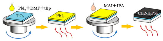
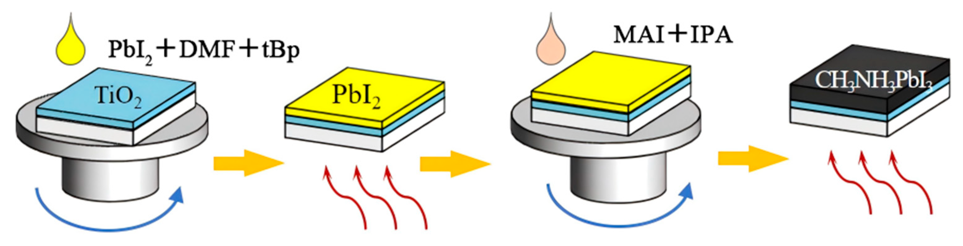
A high-humidity (RH = 40%–50%) two-step deposition method was used to prepare high-quality perovskite films. 4-tert-butylpyridine (tBp) was introduced as an additive in the PbI2 precursor solution. The PbI2 precursor was prepared by dissolving 553 mg of PbI2 in a mixture of 1 mL DMF and 100 μL tBp, while 30 mg of methylammonium iodide (MAI) was dissolved in 1 mL IPA to form the MAI precursor. Both solutions were stirred and heated at 60 °C for 3 h. Next, 70 μL of the PbI2 precursor was deposited onto the mp-TiO2/Au/ITO substrate and spin-coated at 3000 rpm for 60 s, followed by heating at 70 °C for 30 min. Then, 200 μL of the MAI precursor solution was applied onto the substrate and spin-coated at 3000 rpm for 20 s. Finally, the samples were annealed at 95 °C for 30 min to form the perovskite thin film. The overall fabrication process is illustrated in Figure 1.
Figure 1.
Schematic flow chart of the perovskite film fabrication process [28]. The red wavy arrows indicate the thermal annealing step.
2.3. Experimental Setup and Mechanism
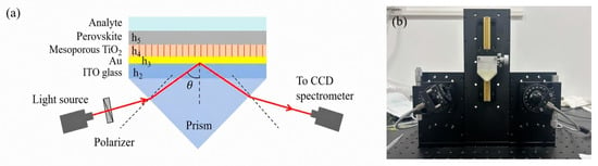
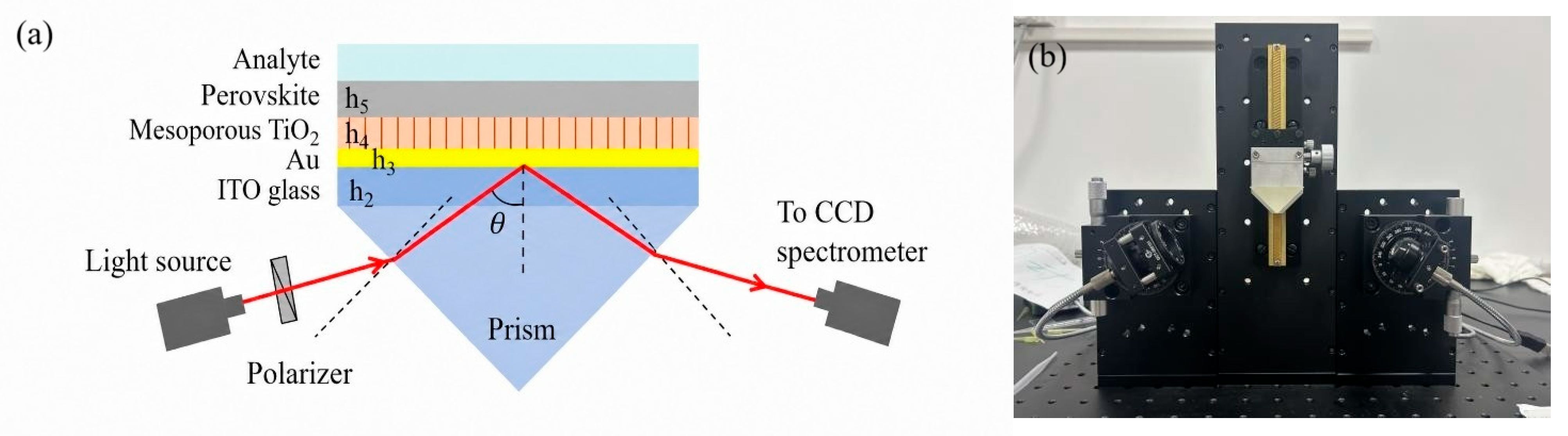
The sensing structure of the proposed perovskite-modified spectrally resolved optical waveguide resonance sensor is schematically shown in Figure 2a, and the corresponding optical detection setup is presented in Figure 2b. The evanescent wave generated by total reflection excites the guided mode in the TiO2 film. A portion of the energy carried by this guided mode is absorbed by the gold film over a short propagation path, while the remaining energy leaks into the glass substrate, forming a leaky mode [29,30].
Figure 2.
(a) Schematic diagram of optical waveguide resonance sensor structure; (b) photograph of the optical detection setup.
The reflection spectra of the proposed sensor are simulated based on Fresnel theory. The reflection coefficient r represents the ratio of the complex amplitude of the reflected light to that of the incident light, which depends on the incident angle and the polarization state of the incident light. For incident light with TE and TM polarization, the reflection coefficients in a two-layer dielectric structure can be expressed as:
where n1 and n2 are the refractive indices of the first and second layers, respectively, and θ1 and θ2 represent the incident and the transmission angles, respectively.
For the five-layer dielectric structure of the sensor proposed in this study (see Figure 2a), the reflection coefficient is expressed as
where the reflection coefficients r12, r23, r34 and r45 correspond to the interfaces between the prism–Au layer, Au-TiO2 layer, TiO2–perovskite layer, and perovskite–analyte, respectively. The parameters k, d, and n represent the wave vector, thickness, and refractive index of each layer, respectively. The indices 1, 2, 3, 4, and 5 refer to the prism, gold, TiO2, perovskite, and analyte, respectively. λ is the wavelength of the incident light. θ1 is the incident angle at the prism-gold interface. The refractive index of each layer can be referred to in Ref. [31].
The overall reflectance R for the five-layer film structure is then obtained as:
For the concentration sensitivity test, analyte solutions of different concentrations were prepared, and the sensor was evaluated in both the four-layer configuration (prism/Au/mesoporous TiO2/analyte) and the five-layer configuration (prism/Au/mesoporous TiO2/perovskite/analyte). To optimize the resonance quality, the incident angle was varied from 11° to 15°. The simulated effect of the incident angle on the resonance characteristics is shown in Figure S1 in the Supplementary Information. The incident angle was then fixed at 13°, and the reflection spectrum of air was first recorded as a reference. Subsequently, the analyte solution was introduced into a small cylindrical cell (radius: 2 mm; height: 2 mm) placed adjacent to the chip, and the cell was sealed. After the vapor phase reached equilibrium and filled the sample chamber (approximately 10 min), the reflection spectrum was recorded. The cell was then emptied, cleaned, and dried, and the spectrum was allowed to return to the air baseline before the next concentration was tested.
3. Results and Discussion
3.1. Simulation of Sensing Characteristics
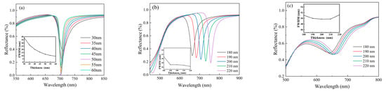
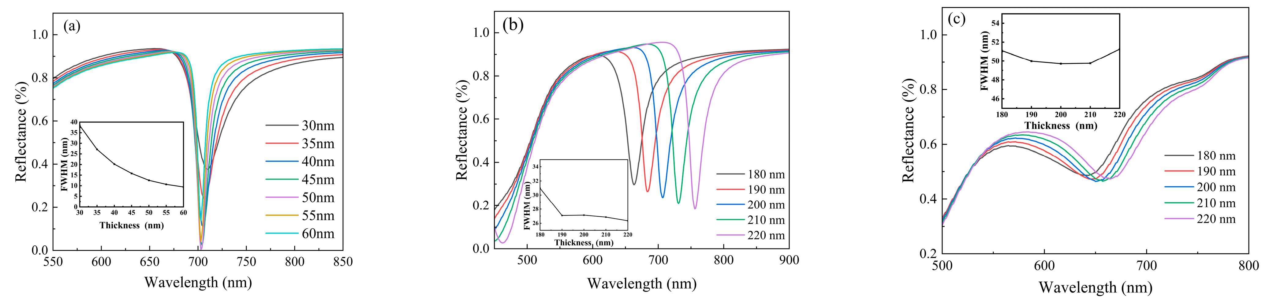
To investigate the influence of individual layer thicknesses on the reflection spectrum and full width at half maximum (FWHM), systematic simulations were carried out based on the Fresnel equations. The incident angle was fixed at 13° under TM polarization, and the thickness of each layer was varied independently while keeping the other parameters constant. The evaluated thickness ranges were 30–60 nm for the Au layer, 180–220 nm for the mesoporous TiO2 layer, and 180–220 nm for the perovskite layer. Figure 3 shows the simulated reflection spectra, with the corresponding FWHM–thickness relationships presented in the insets.
Figure 3.
Simulated reflection spectra for different structural parameters: (a) Au layer thickness varied from 30 to 60 nm; (b) mesoporous TiO2 layer thickness varied from 180 to 220 nm under TM polarization; (c) perovskite layer thickness varied from 180 to 220 nm. Insets show the relationship between FWHM and thickness.
Figure 3a shows the effect of the Au layer thickness on the reflection spectrum when water was used as the analyte. Within the range of 30–60 nm, the Au thickness has only a minor influence on the resonance wavelength, whereas it significantly affects the peak depth and FWHM of the reflection spectrum. As the Au thickness increases from 30 to 60 nm, the FWHM decreases from 38.71 nm to 7.43 nm, indicating a substantial narrowing of the resonance dip.
With the Au thickness fixed at 50 nm, the influence of the mesoporous TiO2 thickness on the reflection spectrum was further examined, as shown in Figure 3b. Under TM polarization, the resonance wavelength undergoes a pronounced redshift as the TiO2 thickness increases, while the FWHM remains almost unchanged. A similar redshift trend is also observed under TE polarization, consistent with the TM behavior.
Finally, the effect of the perovskite layer thickness was simulated with air as the analyte. The Au thickness was kept the same as in the previous simulations, and the mesoporous TiO2 thickness was fixed at 200 nm. As shown in Figure 3c, increasing the perovskite thickness also leads to a clear redshift of the resonance wavelength, with only a marginal effect on the FWHM.
In summary, the simulation results demonstrate that the Au layer thickness exerts a negligible influence on the resonance wavelength but significantly modulates the peak depth and FWHM; increasing the Au thickness effectively reduces the FWHM, thereby improving the signal-to-noise ratio. In contrast, the thicknesses of both the mesoporous TiO2 and perovskite layers strongly affect the resonance wavelength: thicker layers induce a pronounced redshift, while the FWHM remains essentially unchanged.
3.2. Sensor Chip Characterization
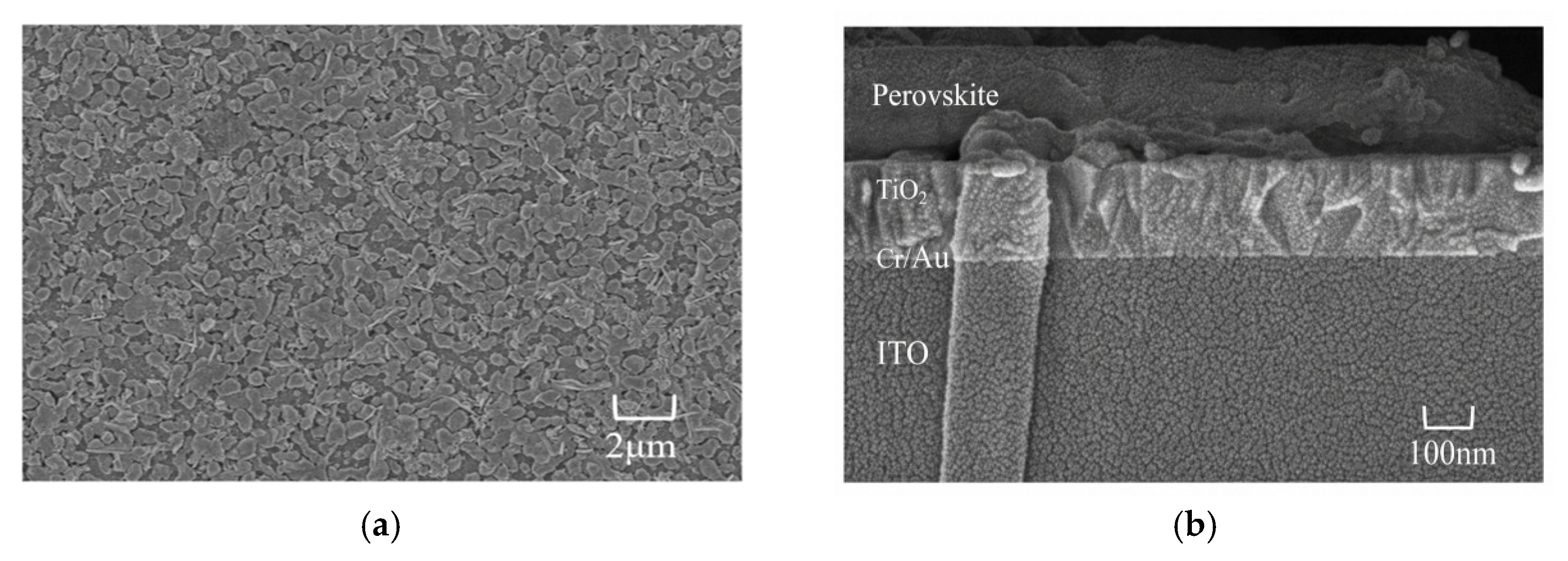
Figure 4a,b shows the surface and cross-sectional morphology images of the perovskite-modified sensor chip obtained by scanning electron microscopy (SEM). The top-view SEM image in Figure 4a reveals that the perovskite film exhibits a granular surface with distinct grain boundaries. This morphology is attributed to the fact that the perovskite layer was prepared in ambient air rather than in an inert-atmosphere glove box. During spin-coating, the hygroscopic N, N-dimethylformamide (DMF) solvent in the precursor solution readily absorbs moisture from the surrounding environment, which lowers the degree of supersaturation and thus reduces the nucleation rate. As a result, the perovskite film grows in an island-like mode, leaving visible gaps between crystallites. Figure 4b presents a cross-sectional SEM image, in which the interfaces between the individual layers can be clearly distinguished. The thicknesses of the mesoporous TiO2 and perovskite film are approximately 200 and 210 nm.
Figure 4.
SEM images of the sensor chip: (a) top-view morphology of the perovskite film; (b) cross-sectional view showing the layer structure.
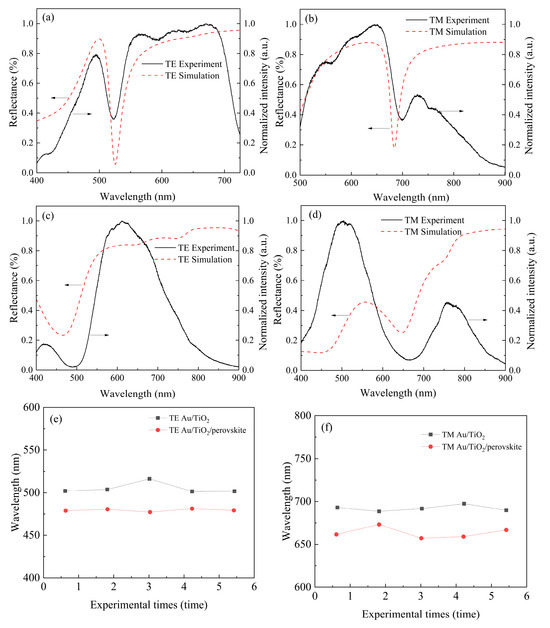
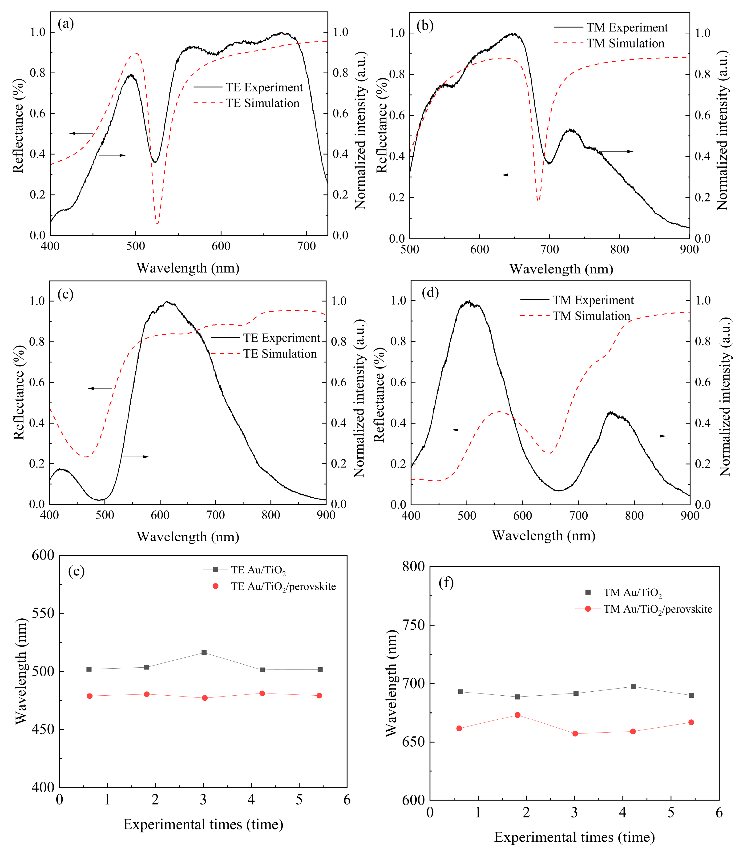
Using the layer thicknesses determined by SEM, the reflection spectra of the four-layer structure (prism/Au/mesoporous TiO2/water) and five-layer structure (prism/Au/mesoporous TiO2/perovskite/air) were simulated for both TE and TM polarization. Figure 5a–d compares the simulated and experimentally measured reflection spectra. Specifically, Figure 5a,b presents the results for the four-layer structure under TE and TM polarization, respectively, while Figure 5c,d shows the corresponding results for the five-layer structure. The resonance peak positions obtained from the simulations agree well with the experimental data, with deviations ranging from 1.3 to 21.8 nm. These deviations can be primarily attributed to the fact that the wavelength-dependent refractive indices used in the simulations were taken from literature values rather than the actual optical constants of the deposited films. Nevertheless, the overall agreement confirms the accuracy and reliability of the Fresnel-based model and suggests that the proposed sensor can also serve as a promising tool for thin-film thickness characterization. Figure 5e,f shows the resonance wavelengths obtained from five repeated experiments using the four-layer and five-layer chip structures, respectively. The maximum standard deviation of the resonance wavelength across all configurations is 5.8 nm, indicating good measurement repeatability. In addition, the batch-to-batch reproducibility across different sensor chips was further investigated. Five sensor chips with perovskite modification were independently fabricated in different batches using identical preparation parameters. The resonance wavelengths of the five chips were 664.98 ± 3.88 nm indicating acceptable batch-to-batch reproducibility (see Figure S2 in the Supplementary Information). The long-term stability over several days was not evaluated in this work and should be addressed in future studies.
Figure 5.
Simulated and experimental reflection spectra and repeatability of the resonance wavelength. (a–d) Comparison of simulated and measured reflection spectra for the four-layer structure under TE (a) and TM (b) polarization, and for the five-layer structure under TE (c) and TM (d) polarization. (e,f) Resonance wavelengths obtained from five repeated measurements for the four-layer (e) and five-layer (f) structures.
3.3. Concentration Sensitivity for Vapor Detection
The vapor sensing performance of the proposed sensor was evaluated using three representative volatile compounds: isopropanol, ammonia, and ethanol. For each analyte, solutions with different concentrations (0–15 wt.%) were prepared, and the reflection spectra were recorded after a 10 min evaporation period to allow vapor equilibrium in the sample chamber. For the sensitivity analysis, the solution concentrations expressed in weight percent (wt.%) were converted to vapor concentrations (mmol/L).
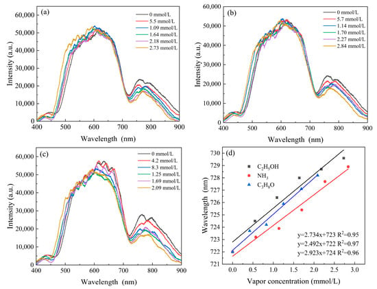
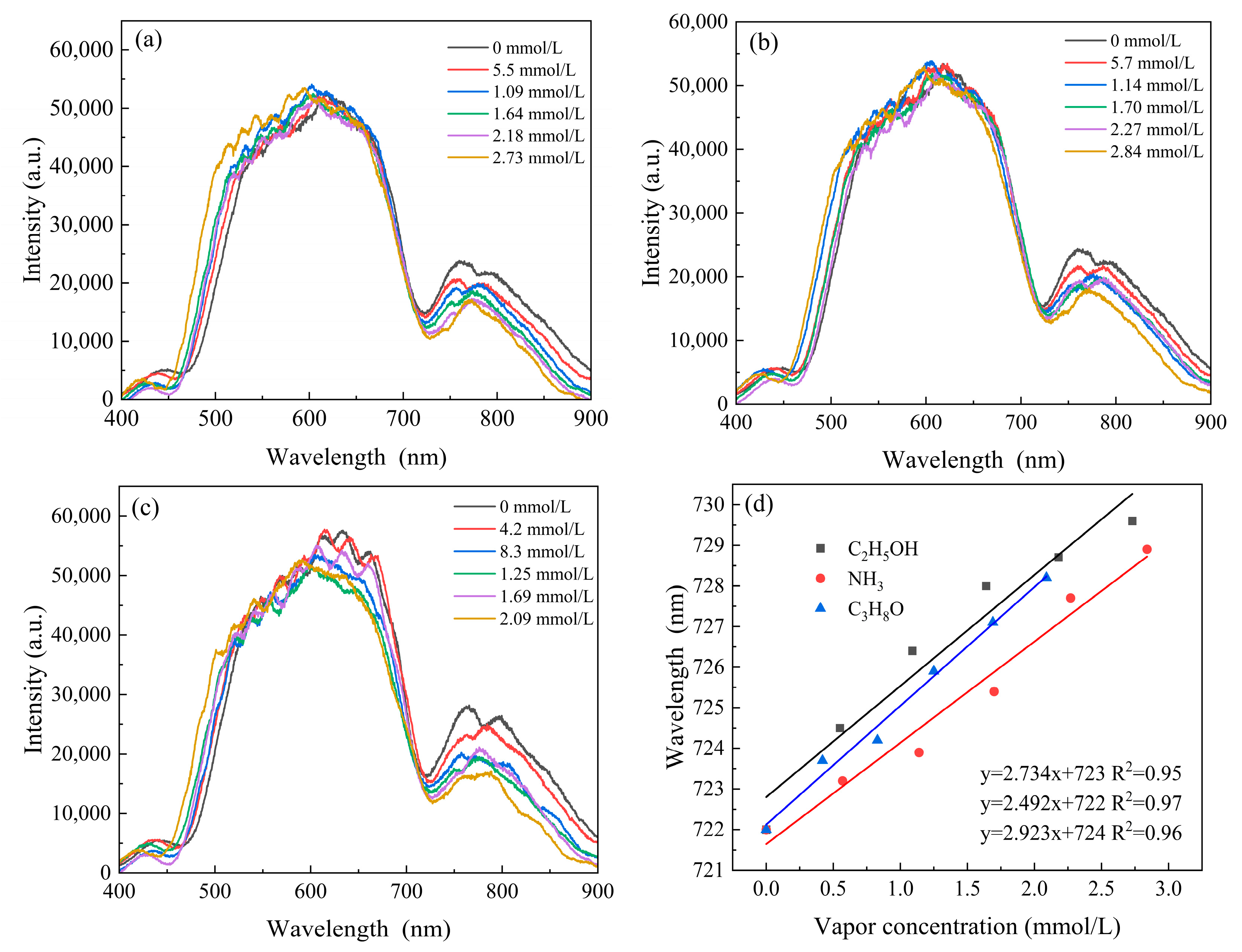
Figure 6a–c shows the reflection spectral responses of the four-layer sensor to ammonia, ethanol, and isopropanol vapors, respectively. In all cases, the resonance wavelength exhibits a clear redshift as the solution concentration increases. Figure 6d summarizes the resonance wavelength as a function of vapor concentration for the three analytes. Linear fitting of the data yields R2 ≥ 0.95 for all three compounds. The resulting sensitivities for ammonia, ethanol, and isopropanol are 2.734, 2.492, and 2.923 nm·L·mmol−1, respectively.
Figure 6.
Reflection spectra of the four-layer structure for detecting different solution concentrations: (a) ammonia, (b) ethanol, (c) isopropanol, and (d) linear fitting of the resonance wavelength versus solution concentration for the three analytes.
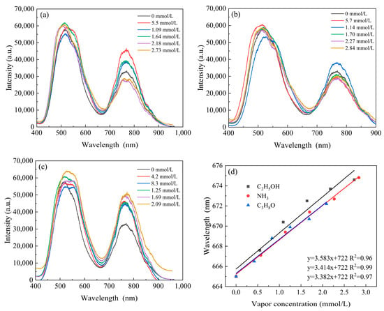
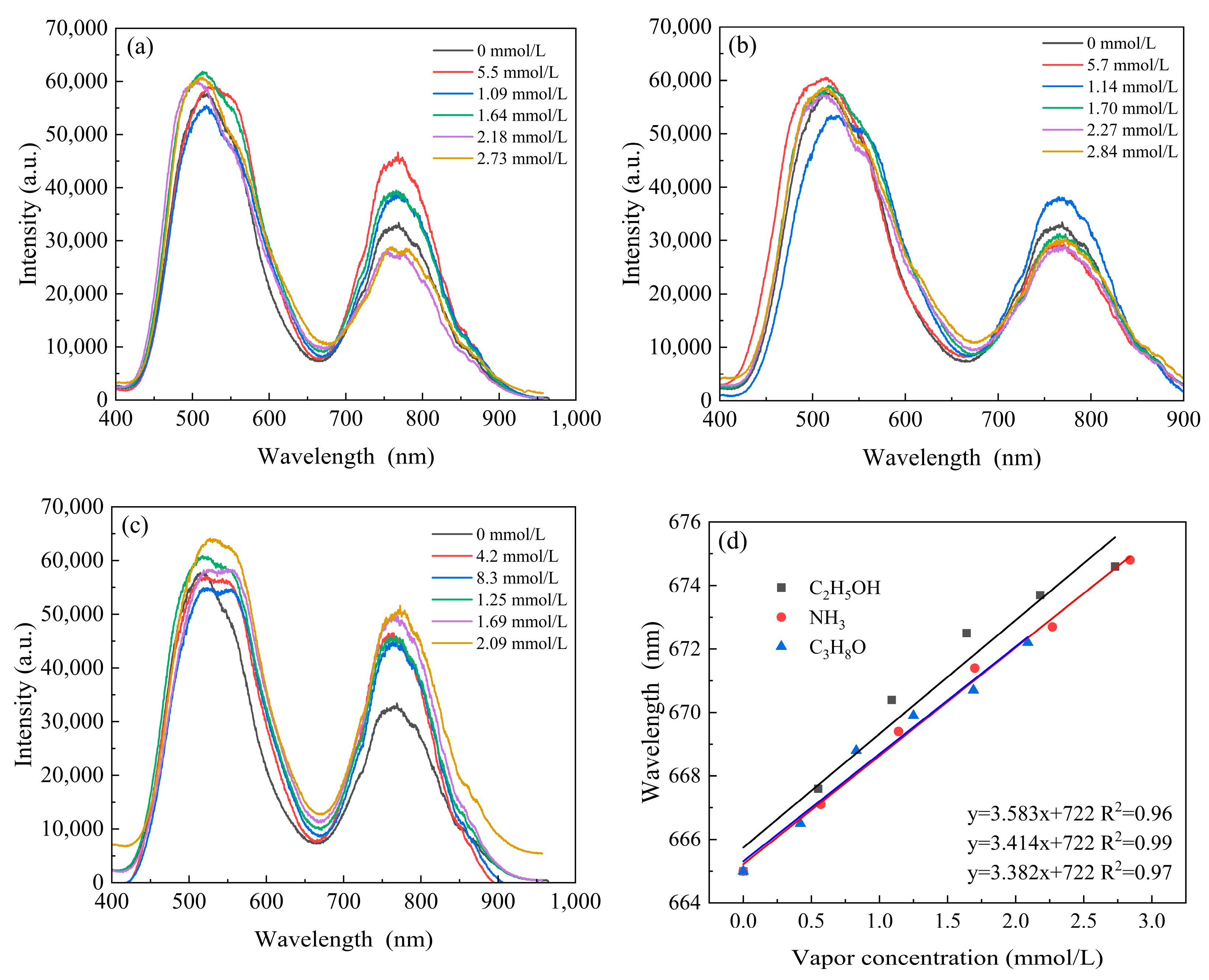
The same experimental procedure was applied to the five-layer sensor after perovskite modification. The reflection spectrum measured with air as the reference medium exhibited a resonance wavelength of 665 nm. Figure 7a–c present the dynamic spectral responses of the five-layer structure to ammonia, ethanol, and isopropanol vapors, respectively. Similarly, the resonance wavelength increases monotonically with increasing solution concentration for all three analytes. Figure 7d plots the resonance wavelength versus solution concentration, and the linear fitting results again show R2 ≥ 0.95 for all compounds. Under the same unit conversion, the five-layer sensor exhibits sensitivity enhancements of approximately 31.1%, 37.0%, and 15.7% for ammonia, ethanol, and isopropanol, respectively, compared with the four-layer structure.
Figure 7.
Reflection spectra of the five-layer structure for detecting different solution concentrations: (a) ammonia, (b) ethanol, (c) isopropanol, and (d) linear fitting of the resonance wavelength versus solution concentration for the three analytes.
To assess the statistical significance of the differences between the sensors (with and without perovskite modification), the 95% confidence intervals of the sensitivities for both sensors and the p-values for the sensitivity differences were calculated. As shown in Table 1, the perovskite-modified sensor exhibited a higher sensitivity than the unmodified sensor for all three analytes. However, the difference was statistically significant only for ethanol (p < 0.05). For ammonia and isopropanol, the differences were not statistically significant (p > 0.05), and their 95% confidence intervals overlapped. In contrast, the 95% confidence intervals for ethanol did not overlap, consistent with the significant difference. These results indicate that the perovskite modification selectively enhances the sensitivity toward ethanol, while its effect on ammonia and isopropanol is not statistically significant. The selective enhancement toward ethanol may be related to its moderate polarity, hydrogen-bonding ability, and suitable molecular size, which could favor interaction with the modified perovskite layer. In contrast, although ammonia is smaller and isopropanol has higher polarizability, their enhancements were not statistically significant, suggesting that these factors alone do not dominate the sensing response. The exact sensing mechanism cannot be determined from the present data and should be explored in future work. It should be noted that the sensor currently exhibits a preferential response toward ethanol rather than strict selectivity, and selectivity in complex vapor mixtures was not evaluated in this work. Future studies will focus on introducing specific recognition sites or selective modification layers on the perovskite surface to enable selective ethanol detection in mixed-vapor environments. Finally, the confidence intervals and p-values reported here were derived from single calibration curves and therefore reflect the precision of the linear regression fits rather than device-to-device reproducibility.
Table 1.
Calibration sensitivity and 95% confidence intervals (CIs) for sensors with and without perovskite modification toward ammonia, ethanol, and isopropanol, along with the p-values for the difference in sensitivity between the two sensors.
The observed redshift of the resonance wavelength with increasing vapor concentration can be attributed to the following synergistic effects: (1) Vapor-phase mass transfer and adsorption equilibrium: Higher solution concentrations generate a greater flux of vapor-phase molecules, leading to increased adsorption onto the waveguide surface and a higher interfacial molecular density. (2) Dielectric environment modification: Adsorbed molecules raise the effective refractive index of the waveguide surface layer through dipole–polarization interactions. (3) Evanescent-field localization enhancement: The penetration depth of the evanescent field increases with the gas-phase refractive index, thereby amplifying the influence of refractive index changes on the resonance condition. (4) Perovskite-layer enhancement: The introduction of the perovskite thin film further increases the effective refractive index of the waveguide structure, which strengthens the confinement of the guided mode and enhances the overlap between the evanescent field and the sensing medium. The enhanced sensitivity may be attributed to changes in the effective refractive index of the perovskite layer upon vapor exposure. While the above classical picture provides a quantitatively adequate description of the observed resonance shift, the underlying physics of the perovskite layer is intrinsically quantum in nature, and a deeper interpretation requires considering the collective light–matter interaction in the active medium. According to the quantum nano-plasmonics framework [32], the classical description is valid only when the system size is much larger than the electron Fermi wavelength and the number of carriers is large. As the confinement scale decreases, the resonance condition is modified by quantum-confinement effects. Within this framework, the plasmon frequency in a confined system is modified by quantum size effects arising from the discretization of electronic states. The crossover from classical to quantum behavior occurs when the classical plasmon energy becomes comparable to the single-particle excitation energy. In this context, the observed resonance can be interpreted as a manifestation of collective light–matter interaction involving excitonic and charge-carrier dynamics. Analyte adsorption may perturb these quantum states, modifying the exciton oscillator strength and effective polarizability of the perovskite layer. This suggests that the enhanced sensitivity may involve quantum-level processes beyond what the classical effective-refractive-index description captures, rather than being fully accounted for by macroscopic dielectric changes alone.
4. Conclusions
In this study, a spectrally resolved optical waveguide resonance (OWR) sensor modified with a perovskite thin film was proposed and experimentally demonstrated for vapor detection. The sensor chip, consisting of an ITO glass substrate coated with Au, mesoporous TiO2, and perovskite layers, was fabricated and systematically characterized. Simulations based on the Fresnel equations revealed that the thickness of the Au layer primarily influences the full width at half maximum (FWHM) of the resonance dip, while the thicknesses of the mesoporous TiO2 and perovskite layers significantly tune the resonance wavelength. The structural parameters determined by scanning electron microscopy were incorporated into the theoretical model, and the simulated reflection spectra showed good agreement with the experimental results, confirming the reliability of the model and indicating the sensor’s potential for thin-film thickness characterization.
The vapor sensing performance was evaluated using ammonia, ethanol, and isopropanol as model analytes. Both the four-layer and five-layer configurations exhibited linear responses of the resonance wavelength to vapor concentration over the tested range (R2 ≥ 0.95). The incorporation of the perovskite layer enhanced the sensitivity, with improvements of approximately 31.1%, 37.0%, and 15.7% for ammonia, ethanol, and isopropanol, respectively. However, only the enhancement for ethanol was statistically significant (p < 0.05); the differences for ammonia and isopropanol were not statistically significant (p > 0.05). This enhancement may be related to the higher effective refractive index introduced by the perovskite layer, which strengthens the evanescent-field interaction. At the quantum level, the observed resonance behavior can also be understood as a scale-dependent collective light–matter interaction in which quantum confinement modifies the classical plasmonic response of the perovskite layer. The sensitivity achieved in this work is comparable to that typically reported for evanescent-field optical sensors.
These results demonstrate that perovskite modification is a promising strategy for improving the performance of OWR sensors, offering enhanced sensitivity, good repeatability, and a simple fabrication route. The proposed sensor provides a valuable platform for volatile organic compound detection and holds potential for applications in environmental monitoring, industrial safety, and chemical sensing.
Supplementary Materials
The following supporting information can be downloaded at https://www.mdpi.com/article/10.3390/coatings16101137/s1. Figure S1: (a) The simulated reflection spectra of the sensor at incident angles from 11° to 15°. (b) Resonance wavelength as a function of incident angle. The resonance wavelength decreases monotonically as the incident angle increases from 11° to 15°. (c) Full width at half maximum (FWHM) of the resonance dip as a function of incident angle. The FWHM reaches its minimum value at 13° (approximately 22.0 nm), indicating the narrowest resonance dip among the tested angles. Figure S2: Resonance wavelengths of five perovskite-modified sensor chips fabricated under identical experimental conditions. Each data point represents the resonance wavelength of one batch, the dashed line indicates the mean value (664.98 nm), and the standard deviation (SD) is 3.88 nm.
Author Contributions
Conceptualization, D.L. and L.C.; methodology, M.L. and L.C.; investigation, C.Y. and P.Z.; writing—original draft, D.L., M.L. and L.C.; writing—review and editing, C.C.; data curation, M.L. and L.C.; funding acquisition, D.L.; project administration, C.C. All authors have read and agreed to the published version of the manuscript.
Funding
This research was supported by the National Natural Science Foundation of China (22274127).
Institutional Review Board Statement
Not applicable.
Informed Consent Statement
Not applicable.
Data Availability Statement
The data presented in this study are available on request from the corresponding authors.
Conflicts of Interest
The authors declare no conflicts of interest.
References
- Ji, Y.H.; Chen, Q.; Wang, Y.M.; Wang, Y.; Li, K. Synthesis of halide perovskite and metal-organic framework composites and their research progress in the field of optoelectronics. Chin. J. Lumin. 2024, 45, 1622–1638. [Google Scholar] [CrossRef] [Scilit]
- Passarelli, J.V.; Mauck, C.M.; Winslow, S.W.; Perkinson, C.F.; Bard, J.C.; Sai, H.; Williams, K.W.; Narayanan, A.; Fairfield, D.J.; Hendricks, M.P.; et al. Tunable exciton binding energy in 2D hybrid layered perovskites through donor–acceptor interactions within the organic layer. Nat. Chem. 2020, 12, 672–682. [Google Scholar] [CrossRef] [Scilit] [PubMed]
- Dey, A.; Ye, J.; De, A.; Debroye, E.; Ha, S.K.; Bladt, E.; Kshirsagar, A.S.; Wang, Z.; Yin, J.; Wang, Y.; et al. State of the art and prospects for halide perovskite nanocrystals. ACS Nano 2021, 15, 10775–10981. [Google Scholar] [CrossRef] [Scilit] [PubMed]
- Jiang, Q.; Zhao, Y.; Zhang, X.W.; Yang, X.; Chen, Y.; Chu, Z.; Ye, Q.; Li, X.; Yin, Z.; You, J. Surface passivation of perovskite film for efficient solar cells. Nat. Photonics 2019, 13, 460–466. [Google Scholar] [CrossRef] [Scilit]
- Lian, X.; Chen, J.; Qin, M.; Zhang, Y.; Tian, S.; Lu, X.; Wu, G.; Chen, H. The second spacer cation assisted growth of a 2D perovskite film with oriented large grains for highly efficient and stable solar cells. Angew. Chem. Int. Ed. 2019, 58, 9409–9413. [Google Scholar] [CrossRef] [Scilit] [PubMed]
- Mączka, M.; Zienkiewicz, J.A.; Ptak, M. Comparative studies of phonon properties of three-dimensional hybrid organic–inorganic perovskites comprising methylhydrazinium, methylammonium, and formamidinium cations. J. Phys. Chem. C 2022, 126, 4048–4056. [Google Scholar] [CrossRef] [Scilit]
- Mahmud, M.A.; Duong, T.; Yin, Y.; Pham, H.T.; Walter, D.; Peng, J.; Wu, Y.; Li, L.; Shen, H.; Wu, N.; et al. Double-sided surface passivation of 3D perovskite film for high-efficiency mixed-dimensional perovskite solar cells. Adv. Funct. Mater. 2020, 30, 1907962. [Google Scholar] [CrossRef] [Scilit]
- Wu, W.; Wang, X.; Han, X.; Yang, Z.; Gao, G.; Zhang, Y.; Hu, J.; Tan, Y.; Pan, A.; Pan, C. Flexible photodetector arrays based on patterned CH3NH3PbI3−xClx perovskite film for real-time photosensing and imaging. Adv. Mater. 2019, 31, 1805913. [Google Scholar] [CrossRef] [Scilit] [PubMed]
- Afre, R.A.; Pugliese, D. Perovskite solar cells: A review of the latest advances in materials, fabrication techniques, and stability enhancement strategies. Micromachines 2024, 15, 192. [Google Scholar] [CrossRef] [Scilit] [PubMed]
- Johnson-Groh, M. Blue perovskite LEDs improved with in situ fabrication technique. Scilight 2024, 2024, 331101. [Google Scholar] [CrossRef] [Scilit]
- Li, X.; Shen, X.; Lv, Q.; Guo, P.; Xiao, L. Metal halide perovskites: Promising materials for light-emitting diodes. Coatings 2024, 14, 83. [Google Scholar] [CrossRef] [Scilit]
- Ai, B.; Fan, Z.; Wong, Z.J. Plasmonic–perovskite solar cells, light emitters, and sensors. Microsyst. Nanoeng. 2022, 8, 5. [Google Scholar] [CrossRef] [Scilit] [PubMed]
- Ma, T.J.; Xue, N.; Muhammad, A.; Fang, G.; Yan, J.; Chen, R.; Sun, J.; Sun, X. Recent progress in photodetectors: From materials to structures and applications. Micromachines 2024, 15, 1249. [Google Scholar] [CrossRef] [Scilit] [PubMed]
- Du, S.J.; Zhang, F.T.; Ma, L. Advances in femtosecond laser synthesis and micromachining of halide perovskites. Light Adv. Manuf. 2024, 5, 35. [Google Scholar] [CrossRef] [Scilit]
- Kojima, A.; Teshima, K.; Shirai, Y.; Miyasaka, T. Organometal halide perovskites as visible-light sensitizers for photovoltaic cells. J. Am. Chem. Soc. 2009, 131, 6050–6051. [Google Scholar] [CrossRef] [Scilit] [PubMed]
- Liu, Z.; Lin, R.; Wei, M.; Yin, M.; Wu, P.; Li, M.; Li, L.; Wang, Y.; Chen, G.; Carnevali, V.; et al. All-perovskite tandem solar cells achieving >29% efficiency with improved (100) orientation in wide-bandgap perovskites. Nat. Mater. 2025, 24, 252–259. [Google Scholar] [PubMed]
- Wang, S.; Li, W.; Yu, C.; Shi, W.; Kang, Q.; Cao, F.; Gao, K.; Yang, L.; Yang, B.; Zhou, J.; et al. Flexible perovskite/silicon tandem solar cells with 33.6% efficiency. Nature 2026, 649, 59–64. [Google Scholar] [CrossRef] [Scilit] [PubMed]
- Yuan, X.; Wu, L.; Qin, Y. Advancing sensitivity in guided-wave surface plasmon resonance sensor through integration of 2D BlueP/MoS2 hybrid layers. Biosensors 2024, 14, 25. [Google Scholar] [CrossRef] [Scilit] [PubMed]
- Li, L.; Zhang, J.; Li, Y.; Huang, C.; Xu, J.; Zhao, Y.; Zhang, P. Dielectric surface-based biosensors for enhanced detection of biomolecular interactions: Advances and applications. Biosensors 2024, 14, 524. [Google Scholar] [CrossRef] [Scilit] [PubMed]
- Makela, M.; Lin, Z.; Lin, P.T. Rapid detection of SARS-CoV-2 genetic targets using nanoporous waveguide based competitive displacement assay. Giant 2023, 15, 100173. [Google Scholar] [CrossRef] [Scilit] [PubMed]
- Al Husseini, D.; Karanth, Y.; Zhou, J.; Willhelm, D.; Qian, X.; Gutierrez-Osuna, R.; Coté, G.L.; Lin, P.T.; Sukhishvili, S.A. Surface functionalization utilizing mesoporous silica nanoparticles for enhanced evanescent-field mid-infrared waveguide gas sensing. Coatings 2021, 11, 118. [Google Scholar] [CrossRef] [Scilit]
- Hoa, X.D.; Kirk, A.G.; Tabrizian, M. Towards integrated and sensitive surface plasmon resonance biosensors: A review of recent progress. Biosens. Bioelectron. 2007, 23, 151–160. [Google Scholar] [CrossRef] [Scilit] [PubMed]
- Vlk, M.; Datta, A.; Alberti, S.; Yallew, H.D.; Mittal, V.; Murugan, G.S.; Jágerská, J. Extraordinary evanescent field confinement waveguide sensor for mid-infrared trace gas spectroscopy. Light Sci. Appl. 2021, 10, 26. [Google Scholar] [CrossRef] [Scilit] [PubMed]
- Zhou, J.; Zhang, Z.; Dong, B.; Ren, Z.; Liu, W.; Lee, C. Midinfrared spectroscopic analysis of aqueous mixtures using artificial-intelligence-enhanced metamaterial waveguide sensing platform. ACS Nano 2023, 17, 711–724. [Google Scholar] [CrossRef] [Scilit] [PubMed]
- Knoll, W.; Azzaroni, O.; Duran, H.; Kunze-Liebhäuser, J.; Lau, K.H.A.; Reimhult, E.; Yameen, B. Nanoporous thin films in optical waveguide spectroscopy for chemical analytics. Anal. Bioanal. Chem. 2020, 412, 3299–3315. [Google Scholar] [CrossRef] [Scilit] [PubMed]
- Han, Q.; Wang, J.; Tian, S.; Hu, S.; Wu, X.; Bai, R.; Zhao, H.; Zhang, D.W.; Sun, Q.; Ji, L. Inorganic perovskite-based active multifunctional integrated photonic devices. Nat. Commun. 2024, 15, 1536. [Google Scholar] [CrossRef] [Scilit] [PubMed]
- Daher, M.G.; Trabelsi, Y.; Ahmed, N.M.; Prajapati, Y.K.; Sorathiya, V.; Ahammad, S.H.; Priya, P.P.; Faragallah, O.S.; Rashed, A.N.Z. Detection of basal cancer cells using a photodetector based on a novel surface plasmon resonance nanostructure employing a perovskite layer with ultra-high sensitivity. Plasmonics 2022, 17, 2365–2373. [Google Scholar] [CrossRef] [Scilit]
- Zhang, Z.Y.; Xiao, Z.H.; Zhu, S.; Zhang, Q.; Xia, R.D.; Peng, J.B. Optical Gain Properties of Interfacial Material PFN-Br and Its Application Potentials in Future Electrically Pumped Organic Lasers. Acta Phys. Sin. 2023, 72, 214204. [Google Scholar] [CrossRef] [Scilit]
- Zhang, Z.; Qi, Z.M. Study of spectral sensitivity to small molecule analytes using TiO2 nanoporous thin-film leaky waveguide resonance sensors. Chin. J. Anal. Chem. 2010, 38, 1538–1543. [Google Scholar] [CrossRef] [Scilit]
- Wang, G.; Wang, C.; Sun, S. An optical waveguide sensor based on mesoporous silica films with a comparison to surface plasmon resonance sensors. Sens. Actuators B Chem. 2018, 255, 3400–3408. [Google Scholar] [CrossRef] [Scilit]
- Lu, D.; Yang, C.; Chen, L.; Wang, M.; Cao, C. Simulation analysis of spectrally-resolved TiO2 optical waveguide resonant sensor modified with perovskite film. Sens. Imaging 2025, 26, 9. [Google Scholar] [CrossRef] [Scilit]
- Jacak, W.A. Quantum Nano-Plasmonics; Cambridge University Press: Cambridge, UK, 2020. [Google Scholar]

Disclaimer/Publisher’s Note: The statements, opinions and data contained in all publications are solely those of the individual author(s) and contributor(s) and not of MDPI and/or the editor(s). MDPI and/or the editor(s) disclaim responsibility for any injury to people or property resulting from any ideas, methods, instructions or products referred to in the content. |
© 2026 by the authors. Licensee MDPI, Basel, Switzerland. This article is an open access article distributed under the terms and conditions of the Creative Commons Attribution (CC BY) license.