Abstract
Deposition of a heteroepitaxial TiHfN film with a growth rate of about 1 μm/h was successfully achieved on a Si (001) substrate at a temperature above 700 °C by direct current magnetron reactive sputtering of a Ti0.6Hf0.4 (in atomic fraction) target with an Ar/N2 gas mixture. Annealing of the as-deposited TiHfN/Si sample at a temperature above 1000 °C using microwave plasma with H2/N2 gas was performed to further improve the TiHfN film’s quality. X-ray diffraction results show that the heteroepitaxial TiHfN film on Si exhibits a cube-on-cube relationship as {001}TiHfN//{001}Si and <110>TiHfN//<110>Si. X-ray rocking curve measurements show that the full width at half maximum of (200)TiHfN is 1.36° for the as-deposited TiHfN film, while it is significantly reduced to 0.53° after microwave plasma annealing. The surface morphologies of the as-deposited and annealed TiHfN films are smooth, with a surface roughness of around ~2 nm. Cross-sectional scanning/transmission electron microscopy (S/TEM) shows a reduction in defects in the annealed film, and X-ray photoelectron spectroscopy shows that the film composition remains unchanged. Additionally, S/TEM examinations with atomic resolution illustrate domain matching epitaxy (DME) between TiHfN and Si at the interface. The TiHfN films have good electrical conducting properties with resistivities of 40–45 μΩ·cm.
1. Introduction
Transition metal nitrides have many outstanding material properties, including high hardness, high thermal stability, good electrical conductivity and chemical inertness [1,2,3,4,5]. Those properties mean transition metal nitride has a high potential for many industrial applications [6,7]. Recently, transition metal nitrides, such as HfN and TiN, which are conductive, have been considered for a variety of electronic, photonic and plasmonic applications [8]. The ternary TiHfN compounds can form a solid solution at high temperatures due to both TiN and HfN having a rock salt structure and similar properties [9,10,11]. Similar to other ternary transition metal nitrides, TiHfN may have better thermal stability and higher hardness than TiN and HfN [12].
TiHfN films have been deposited by arc ion plating [6,7,13] and sputtering [14] in previous studies. However, the deposited TiHfN films were polycrystalline. If an epitaxial film can be obtained, it may enhance the understanding of basic TiHfN properties. Heteroepitaxial growth of TiN [15,16,17] and HfN [18,19] has been commonly performed on Si substrates with domain matching epitaxy (DME) [20]. The lattice parameters of TiHfN range from 4.240 to 4.525 Å, depending on the atomic ratio of Ti/Hf. According to first-principles calculations, Ti0.6Hf0.4N (in atomic ratio of Ti/Hf) has a higher formation energy than other compositions, and it is in a solid solution above 700–900 K from the calculated phase diagram [10]. The lattice parameter of Ti0.6Hf0.4N has been evaluated to be around 4.38 Å [21,22], which gives approximately a 5/4 matching between Ti0.6Hf0.4N and Si for DME. Hence, Ti0.6Hf0.4N films with high crystallinity can be expected to be deposited on Si substrates. However, for TiHfN deposition on Si by reactive sputtering, the formation of silicon nitride and silicide on the surface of Si under N-rich and N-poor conditions needs to take into consideration. For the growth of a cubic (001) HfN film on a Si (001) substrate in our recent study, we observed that epitaxial orthorhombic HfSi2 forms between HfN and Si [23]. Additionally, theoretical calculations of the phase diagram of TiN-HfN show that TiHfN is of a single phase at high temperatures, while a miscibility gap exists at low temperatures [10]. Nevertheless, epitaxial growth of TiHfN on Si is rarely reported.
Furthermore, annealing can significantly improve the crystalline quality of the thin film. Knotek et al. have shown that the Ti0.3Hf0.7N films retained an initial single-phase structure after annealing at 1000 °C for 24 h [11]. Recently, we have shown that the crystalline quality of the epitaxial TiZrN film can be effectively improved by microwave plasma heating [24]. Similarly, it is expected that the TiHfN film may have better crystalline quality after high-temperature microwave plasma annealing. In this work, heteroepitaxial TiHfN films on a Si (001) substrate are successfully grown by reactive direct current magnetron sputtering (DCMS) deposition, and the film quality is further improved by microwave plasma annealing.
2. Materials and Methods
TiHfN films were deposited on p-type (001) Si substrates with a size of 1 × 1 cm2 by reactive DCMS with a 2-inch Ti0.6Hf0.4 alloy target (99.9% purity). Before loading in the vacuum sputter chamber, the substrates were ultrasonically cleaned in sequence with acetone, methanol and ethanol, each for 10 min. Finally, the surface oxide was removed by dipping the substrates in 6% HF, followed by drying with nitrogen gas. After the pressure was evacuated to below 8 × 10⁻⁶ mbar, the temperature of the stage was heated at 750 °C for 1 h to reduce the residual gas contamination in the vacuum. The substrate temperature was measured by an optical pyrometer. Prior to deposition, the TiHf alloy target was pre-sputtered with pure Ar plasma for 5 min to clean any contamination and oxide on the surface. The working pressure for sputtering was maintained at 4 × 10⁻³ mbar. The N2 flow in Ar was set at 9% for the present work. The sputtering time was 8 min. The working distance between the TiHf target and Si substrate was set at 12 cm, and the DC power was 65 W. After sputtering, the sample was cooled to room temperature under Ar/N2 ambient conditions.
For subsequent annealing of the as-deposited TiHfN film, the TiHfN/Si sample was placed on a Mo holder and loaded into a microwave plasma system (ASTeX, 2.45 GHz, MA, USA). The annealing process was similar to that used for TiZrN films [24], and for plasma nitridation of sapphire and TiO2 to obtain epitaxial AlN and TiN, as shown in our previous studies [25,26,27]. The surface of the TiHfN film was first cleaned with pure hydrogen plasma at a microwave power of 300 W and a pressure of 13 mbar for 5 min, followed by plasma annealing with a gas flow rate of 400 sccm (2.5% H2/N2), a power of 800 W and a pressure of 90 mbar for 2 h. The temperature of plasma annealing was 1000–1100 °C, as measured by the optical pyrometer. After the plasma was turned off, the sample was cooled to room temperature at 13 mbar with a gas mixture of 2.5% H2/N2.
High-resolution X-ray diffraction (XRD, BRUKER, D8 DISCOVER, Billerica, MA, USA) was applied to examine the lattice parameter and quality of TiHfN films using techniques including 2θ-ω, ω (rocking curve) and ϕ-scans. The surface roughness of the TiHfN films was measured by atomic force microscopy (AFM, Bruker, Edge-AFM, Billerica, MA, USA). The chemical compositions of the TiHfN films were determined by using X-ray photoelectron spectroscopy (XPS, ULVAC-PHI, PHI QuanteraII, Chigasaki, Japan) with a monochromatic Al Kα radiation source. Argon ion sputtering was used to obtain the XPS depth profiles with a sputtering rate of ~20–25 nm/min. Microstructural observations of the samples in a cross-section view were carried out in a S/TEM (JEOL, ARM200F, Tokyo, Japan) at 200 kV. Cross-sectional TEM specimens were prepared by a focused ion beam (FIB, TESCAN, LYRA3, Brno, Czechia) with Pt protective coating. Electrical resistivity measurements were conducted by a four-point probe measurement (Tektronix, Keithley 2400, Cleveland, OH, USA).
3. Results and Discussion
The 2θ-ω XRD pattern of the as-deposited TiHfN film on a Si substrate is shown in Figure 1a. The (002)Si, (002)TiHfN, (004)Si and (004)TiHfN peaks can be clearly observed. It is apparent that the deposited TiHfN film is in the <001> orientation on the Si (001) substrate. The out-of-plane lattice parameter of TiHfN was determined to be 4.368 ± 0.004 Å from the interplanar spacings of the (002)TiHfN and (004)TiHfN peaks, which is close to the value of Ti0.6Hf0.4N derived in reference [21]. The crystal orientation relationship between TiHfN and Si can be determined by ϕ-scan patterns using the {113}TiHfN and {113}Si reflections. As shown in Figure 1b, both TiHfN and Si in the ϕ-scan patterns have four peaks located at the same angles and separated by a 90° interval. Therefore, it is evident that the TiHfN film is epitaxially deposited on the Si substrate with a cube-on-cube orientation relationship of {001}TiHfN//{001}Si and <110>TiHfN//<110>Si. Figure 1c shows that the full width at half-maximum (FWHM) of the (002)TiHfN X-ray rocking curve (XRC) was 1.36° and the average FWHM of TiHfN peaks in the ϕ-scan was about 3.2°, suggesting that the epitaxial TiHfN film has a reasonably good quality.
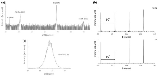
Figure 1.
XRD analyses of the as-deposited TiHfN/Si sample. (a) 2θ−ω pattern, (b) ϕ−scan patterns of {113}TiHfN and {113}Si reflections and (c) (002)TiHfN rocking curve.
The TiHfN/Si sample was further annealed by using microwave plasma. The 2θ-ω XRD pattern of the annealed TiHfN/Si sample is shown in Figure 2a. Similar to the observations on the XRD pattern of the as-deposited film on Si in Figure 1a, there are only peaks belonging to (002)Si, (002)TiHfN, (004)Si and (004)TiHfN, with no other reflections, indicating that the annealed film maintains a single cubic phase. The out-of-plane lattice parameter of the annealed TiHfN film was about 4.360 ± 0.004 Å, slightly lower than that before annealing (4.368 Å). The ϕ-scan patterns in Figure 2b show only {113}TiHfN and {113}Si reflections as well. Therefore, the annealed TiHfN film still retains the same heteroepitaxial relationship with Si as presented above for the as-deposited film. The average FWHM of ϕ-scan peaks of TiHfN was reduced to 1.4° after plasma annealing, indicating the reduction in the extent of in-plane twists. The XRC FWHM value of the (002)TiHfN reflection in Figure 2c is 0.53°, which is far less than that of the as-deposited film (1.36°). From the above results, the crystalline quality of the epitaxial TiHfN film on Si can be significantly improved by plasma annealing. Additionally, the annealed TiHfN film of a single phase shows that it has good thermal stability under the annealing conditions.
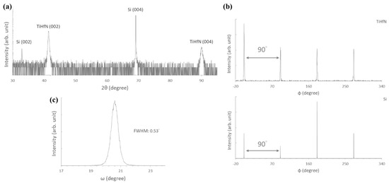
Figure 2.
XRD analyses of the annealed TiHfN/Si sample. (a) 2θ−ω pattern, (b) ϕ−scan patterns of {113}TiHfN and {113}Si reflections and (c) (002)TiHfN rocking curve.
AFM images in Figure 3a,b show the surface morphologies of the as-deposited and annealed TiHfN films, respectively, from which the surface roughness root mean square value was determined to be 1.6 and 2.1 nm, respectively, indicating that the surface of the annealed TiHfN film remains almost as smooth as the as-deposited film.
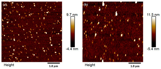
Figure 3.
AFM images in a scan area of 5 × 5 μm2 of the TiHfN/Si samples: (a) as-deposited and (b) annealed films.
The XPS depth profiles of the as-deposited and annealed TiHfN/Si samples are shown in Figure 4a,b, respectively. For the as-deposited film, the N/(Ti + Hf) ratio was around 50/50, and the Ti/Hf ratio was about 60/40, corresponding to the composition of the target alloy. The uniform film composition through the whole film implies a constant rate of reactive sputtering during the deposition. After plasma annealing, the N/(Ti + Hf) ratio was close to 51.5/48.5 in the TiHfN film, and the Ti/Hf ratio remained almost the same as before annealing. As the N/(Ti + Hf) ratio was > 1, this indicates that the annealed film was slightly enriched with nitrogen, which might be caused by the microwave plasma containing a high concentration of nitrogen species/radicals. It is interesting that after annealing, the nitrogen concentration also retains a uniform distribution in depth. At the end of the experiment, the composition of the plasma-annealed TiHfN film had barely changed.
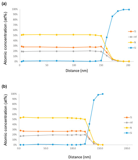
Figure 4.
XPS depth profiles of the TiHfN/Si samples: (a) as-deposited and (b) annealed films.
Furthermore, the binding characteristics of the as-deposited and annealed TiHfN films were studied from the XPS spectra shown in Figure 5a–c. For the as-deposited TiHfN, Figure 5a shows a doublet of the Ti 2p1/2 and 2p3/2 signals at 454.5 and 460.5 eV, with an interval of about 6 eV, suggesting that Ti-N in TiHfN has the same binding characteristics as that in TiN [28]. Figure 5b shows Hf 4f7/2 and 4f5/2 peaks at 15.0 and 16.7 eV, with a ratio of integrated intensity of 4/3. The binding energies are the same as those of Hf-N in HfN, suggesting that Hf in the TiHfN is adjacent to N [29,30]. Figure 5c shows the XPS spectra of the N 1s signal at ~397.2 eV, which is typical of an N atom bonding with Ti or Hf, as the binding energies in TiN and HfN nitrides are consistent with Ti and Hf binding characteristics [28,31]. After plasma annealing, the XPS spectra of Ti 2p, Hf 4f and N1s exhibited no apparent differences from those of the as-deposited TiHfN, indicating that the binding characteristics remain almost unchanged in the annealed film.
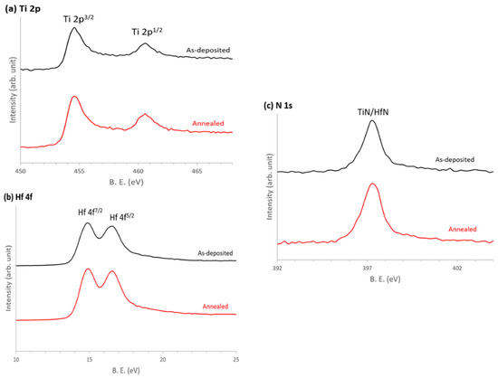
Figure 5.
XPS spectra of the as-deposited and annealed TiHfN/Si samples. (a) Ti 2p, (b) Hf 4f and (c) N 1s.
Figure 6a,b show typical cross-sectional bright-field (BF) TEM micrographs of the as-deposited and annealed TiHfN/Si, respectively. The cross-sectional TEM micrograph in Figure 6a shows that the film thickness is about 160 nm, indicating a corresponding deposition rate of 1.2 µm/h. Additionally, the defects in the deposited film, shown in dark contrast, suggest that the defect density is high, in agreement with the XRC FWHM. For the annealed film in Figure 6b, the film thickness is uniform with a relatively smooth surface and a flat interface, implying that the film is thermally stable under the plasma. As most of the annealed film exhibits a strong bright contrast, it is believed that a significant reduction in defects has occurred after annealing in comparison with the as-deposited film, which is consistent with the XRC results. The appearance of a ~10 nm surface layer with relatively dark phase contrast in Figure 6b is caused by oxidation of the annealed film after exposure to the ambient air for a few weeks before TEM specimen preparation. The as-deposited film had been exposed to air for a shorter period.
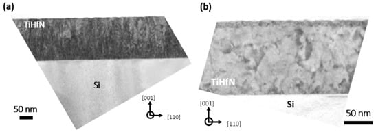
Figure 6.
Cross-sectional BF TEM micrographs of (a) the as-deposited and (b) annealed TiHfN/Si samples taken along the [10] zone axis.
Figure 7a shows a typical cross-sectional high-resolution TEM (HRTEM) image obtained from the TiHfN/Si interfacial region in the as-deposited film with the corresponding fast Fourier transform (FFT) diffraction pattern in Figure 7b. The FFT pattern shows only reflections of TiHfN and Si in the <110> zone axis, without additional diffraction signals, indicating that the as-deposited TiHfN/Si samples have the epitaxial relationship of {001}TiHfN//{001}Si and <110>TiHfN//<110>Si, corresponding well to the XRD results. Furthermore, the Z-contrast atomic-resolution STEM image in Figure 7c shows approximately a 5/4 match between the atomic arrangement of Ti0.6Hf0.4N/Si, corresponding well to the value calculated in the literature [21,22], which is evident for the DME at the interface. Additionally, it was observed that no intermediate compounds, such as silicide and silicon nitride, exist between TiHfN and Si at the interface, implying that TiHfN is directly grown on the surface of the Si substrate.
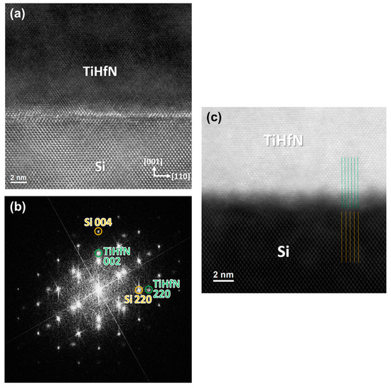
Figure 7.
Cross-sectional S/TEM images of the as-deposited TiHfN/Si interface taken along the [10] zone axis. (a) HRTEM image, (b) the FFT pattern of (a), and (c) the STEM image in Z-contrast.
The out-of-plane (a⊥) and in-plane (a||) lattice parameters of the TiHfN films can be deduced from X-ray reciprocal space mapping (RSM) results (not shown). For the as-deposited TiHfN, a⊥ was 4.368 ± 0.002 Å and a|| was 4.374 ± 0.002 Å. After plasma annealing, the a⊥ and a|| values were 4.360 ± 0.002 Å and 4.368 ± 0.002 Å, respectively. For a cubic structure, the relaxed lattice parameter, a0, can be determined from Equation (1):
where ν is the Poisson ratio. The value of ν used was 0.226, as calculated from Vegard’s law for νTiN = 0.22 and νHfN = 0.25 [32,33]. After substituting the values of a⊥ and a|| into Equation (1), a0 was calculated to be 4.370 Å and 4.363 Å for the as-deposited and the annealed TiHfN films, respectively. The lattice parameter of TiHfN film decreased slightly as the N/(Ti + Hf) ratio increased. Additionally, if a⊥ and a|| were determined from the HRTEM lattice fringes of TiHfN and Si with the FFT patterns, a0 = 4.375 Å and 4.365 Å, within experimental error, can be obtained for the as-deposited and annealed TiHfNs, respectively. The smaller lattice parameter for the annealed TiHfN may be related to the N-rich composition. This is supported by previous reports that show a decrease in the a0(x) of both TiNx and HfNx with an increase in the N/Ti and N/Hf values [32,33].
The calculated phase diagram shows that two phases may coexist in equilibrium in such a temperature range. However, from the above results, the TiHfN film in a single phase is stable after growth at 700–750 °C followed by vacuum cooling, and does not result in the decomposition of TiHfN into TiN-rich and HfN-rich phases. Either a single phase might be present or the decomposition rate might be very low, which may be worthy for further investigation. Additionally, under the plasma conditions for annealing and the following cooling, even with hydrogen in the plasm, TiHfN was thermally stable after annealing above 1000 °C. Both of the measured film resistivities for the as-deposited and annealed TiHfN were in the range of 40–45 μΩ·cm, indicating that ternary nitride is a good electrical conductor.
4. Conclusions
Heteroepitaxial growth of a Ti0.6Hf0.4 film on a Si (001) substrate has been successfully demonstrated by DC magnetron reactive sputtering of a Ti0.6Hf0.4 alloy target with a gas mixture of N2 and Ar. The TiHfN film on the Si (001) substrate exhibits a cube-on-cube epitaxial relationship of {001}TiHfN//{001}Si and <110>TiHfN//<110>Si. The (002)TiHfN XRC FWHM is 1.36°, indicating that the epitaxial TiHfN film is of good quality. The TiHfN film remains in epitaxy with Si after microwave plasma annealing. The crystallinity of the annealed TiHfN film is significantly improved, as the (200)TiHfN XRC FWHM is reduced to 0.53°. Additionally, the S/TEM results show evidence of DME between TiHfN and Si with a ratio of 5/4. Overall, the TiHfN film has good electrical conducting properties with resistivities of 40–45 μΩ·cm.
Author Contributions
Conceptualization, K.-A.C. and L.C.; methodology, F.-H.S., Y.-S.F., W.-C.C. and T.-H.D.; software, F.-H.S.; validation, F.-H.S.; formal analysis, F.-H.S., W.-C.C. and L.C.; investigation, F.-H.S., Y.-S.F., W.-C.C. and P.-H.W.; resources, L.C.; data curation, F.-H.S., K.-A.C., P.-H.W., T.-H.D. and L.C.; writing—original draft preparation, P.-H.W. and K.-A.C.; writing—review and editing, K.-A.C. and L.C.; visualization, P.-H.W. and K.-A.C.; supervision, L.C.; project administration, L.C.; funding acquisition, L.C. All authors have read and agreed to the published version of the manuscript.
Funding
This work was supported by the Ministry of Science and Technology, Taiwan, China under contract of 107-2221-E-009-009-MY2 and 110-2221-E-A49-100.
Institutional Review Board Statement
Not applicable.
Informed Consent Statement
Not applicable.
Data Availability Statement
Not applicable.
Conflicts of Interest
The authors declare no conflict of interest.
References
- Pierson, H.O. Handbook of Refractory Carbides and Nitrides; Noyes Press: Park Ridge, NM, USA, 1996; pp. 181–208. [Google Scholar]
- Sproul, W. Very high rate reactive sputtering of TiN, ZrN and HfN. Thin Solid Films 1983, 107, 141–147. [Google Scholar] [CrossRef]
- Musil, J.; Štěpánek, I.; Kolego, M.; Bláhová, O.; Vyskočil, J.; Kasl, J. Properties of TiN, ZrN and ZrTiN coatings prepared by cathodic arc evaporation. Mater. Sci. Eng. A 1993, 163, 211–214. [Google Scholar]
- Shin, C.-S.; Gall, D.; Hellgren, N.; Patscheider, J.; Petrov, I.; Greene, J.E. Vacancy hardening in single-crystal TiNx (001) layers. J. Appl. Phys. 2003, 93, 6025–6028. [Google Scholar] [CrossRef]
- Valerini, D.; Signore, M.; Tapfer, L.; Piscopiello, E.; Galietti, U.; Rizzo, A. Adhesion and wear of ZrN films sputtered on tungsten carbide substrates. Thin Solid Film. 2013, 538, 42–47. [Google Scholar] [CrossRef]
- Lugscheider, E.; Knotek, O.; Barimani, C.; Zimmermann, H. Arc PVD-coated cutting tools for modern machining applications. Surf. Coat. Technol. 1997, 94, 641–646. [Google Scholar] [CrossRef]
- Bobzin, K.; Bagcivan, N.; Immich, P.; Warnke, C.; Klocke, F.; Zeppenfeld, C.; Mattfeld, P. Advancement of a nanolaminated TiHfN/CrN PVD tool coating by a nano-structured CrN top layer in interaction with a biodegradable lubricant for green metal forming. Surf. Coat. Technol. 2009, 203, 3184–3188. [Google Scholar] [CrossRef]
- Patsalas, P.; Kalfagiannis, N.; Kassavetis, S.; Abadias, G.; Bellas, D.; Lekka, C.; Lidorikis, E. Conductive nitrides: Growth principles, optical and electronic properties, and their perspectives in photonics and plasmonics. Mater. Sci. Eng. R 2018, 123, 1–55. [Google Scholar] [CrossRef]
- Abadias, G.; Koutsokeras, L.E.; Dub, S.N.; Tolmachova, G.N.; Debelle, A.; Sauvage, T.; Villechaise, P. Reactive magnetron cosputtering of hard and conductive ternary nitride thin films: Ti–Zr–N and Ti–Ta–N. J. Vac. Sci. Technol. A 2010, 2, 541–551. [Google Scholar] [CrossRef]
- Liu, Z.T.Y.; Burton, B.P.; Khare, S.V.; Gall, D. First-principles phase diagram calculations for the rocksalt-structure quasibinary systems TiN–ZrN, TiN–HfN and ZrN–HfN. J. Phys. Condens. Matter 2017, 29, 035401. [Google Scholar] [CrossRef]
- Knotek, O.; Atzor, M.; Barimani, A.; Jungblut, F. Development of low temperature ternary coatings for high wear resistance. Surf. Coat. Technol. 1990, 42, 21–29. [Google Scholar] [CrossRef]
- Holleck, H. Binäre und Ternäre Carbid-und Nitridsysteme der Übergangsmetalle; Bornträger: Berlin, Germany, 1984. [Google Scholar]
- Lugscheider, E.; Bobzin, K.; Piñero, C.; Klocke, F.; Massmann, T. Development of a superlattice (Ti,Hf,Cr)N coating for cold metal forming applications. Surf. Coat. Technol. 2004, 17, 616–622. [Google Scholar] [CrossRef]
- Takeyama, M.B.; Sato, M.; Aoyagi, E.; Noya, A. Characterization of TiHfN ternary alloy films as a barrier between Cu plug and Si. Jpn. J. Appl. Phys. 2014, 53, 045019. [Google Scholar] [CrossRef]
- Narayan, J.; Tiwari, P.; Chen, X.; Singh, J.; Chowdhury, R.; Zheleva, T. Epitaxial growth of TiN films on (100) silicon substrates by laser physical vapor deposition. Appl. Phys. Lett. 1992, 61, 1290–1292. [Google Scholar] [CrossRef]
- Sheu, W.-H.; Wu, S.-T. Epitaxial growth of TiN(100) on Si(100) by reactive magnetron sputtering at low temperature. Jpn. J. Appl. Phys. 1998, 37, 3446–3449. [Google Scholar] [CrossRef]
- Choi, C.; Hultman, L.; Chiou, W.; Barnett, S.A. Growth of epitaxial TiN thin films on Si(100) by reactive magnetron sputtering. J. Vac. Sci. Technol. B 1991, 9, 221–227. [Google Scholar] [CrossRef]
- Shinkai, S.; Sasaki, K. Influence of sputtering parameters on the formation process of high-quality and low-resistivity HfN thin film. Jpn. J. Appl. Phys. 1999, 38, 2097–2102. [Google Scholar] [CrossRef]
- Araujo, R.A.; Zhang, X.; Wang, H. Cubic HfN thin films with low resistivity on Si (001). J. Electron. Mater. 2008, 37, 1828–1831. [Google Scholar] [CrossRef]
- Narayan, J.; Larson, B.C. Domain epitaxy: A unified paradigm for thin film growth. J. Appl. Phys. 2003, 93, 278–285. [Google Scholar] [CrossRef]
- Nowotny, H.; Benesovsky, F.; Rudy, E. Hochschmelzende Systeme mit Hafniumkarbid und-nitrid. Mon. für Chem. 1960, 91, 348–356. [Google Scholar] [CrossRef]
- Ou, P.; Wang, J.; Shang, S.; Chen, L.; Du, Y.; Liu, Z.; Zheng, F. A first-principles study of structure, elasticity and thermal decomposition of Ti1−xTMxN alloys (TM=Y, Zr, Nb, Hf, and Ta). Surf. Coat. Technol. 2015, 264, 41–48. [Google Scholar] [CrossRef]
- Fang, Y.-S.; Chiu, K.-A.; Do, H.; Chang, L. Reactive sputtering for highly oriented HfN film growth on Si (100) substrate. Surf. Coat. Technol. 2019, 377, 124877. [Google Scholar] [CrossRef]
- Chiu, K.-A.; Fu, C.-W.; Fang, Y.-S.; Do, T.H.; Shih, F.-H.; Chang, L. Heteroepitaxial growth and microwave plasma annealing of DC reactive sputtering deposited TiZrN film on Si (100). Surf. Coat. Technol. 2020, 394, 125873. [Google Scholar] [CrossRef]
- Ma, Z.-C.; Chiu, K.-A.; Wei, L.-L.; Chang, L. Formation of m-plane AlN on plasma-nitrided m-plane sapphire. Jpn. J. Appl. Phys. 2019, 58, SC1033. [Google Scholar] [CrossRef]
- Chen, Y.-C.; Chang, L. Epitaxial AlN on c-plane sapphire by plasma nitriding. Jpn. J. Appl. Phys. 2019, 58, SC1012. [Google Scholar] [CrossRef]
- Do, T.H.; Chang, C.; Wei, L.-L.; Chiu, K.-A.; Chang, L. Epitaxial TiN formation on rutile titanium dioxide (001) single crystal by nitridation. Appl. Surf. Sci. 2020, 506, 144614. [Google Scholar] [CrossRef]
- Ino, T.; Kamimuta, Y.; Suzuki, M.; Koyama, M.; Nishiyama, A. Dielectric constant behavior of Hf–O–N system. Jpn. J. Appl. Phys. 2006, 45, 2908–2913. [Google Scholar] [CrossRef]
- Arranz, A. Synthesis of hafnium nitride films by 0.5–5 keV nitrogen implantation of metallic Hf: An X-ray photoelectron spectroscopy and factor analysis study. Surf. Sci. 2004, 563, 1–12. [Google Scholar] [CrossRef]
- Bruninx, E.; Van Eenbergen, A.F.P.M.; Van Der Werf, P.; Haisma, J. X-ray photoelectron spectroscopy of hafnium nitride. J. Mater. Sci. 1986, 21, 541–546. [Google Scholar] [CrossRef]
- Kar, S.; Misra, D.; Singh, R.; Gonzalez, F. Physics and Technology of High-k Gate Dielectrics I; The Electrochemical Society: Pennington, NJ, USA, 2002. [Google Scholar]
- Shin, C.-S. Growth, surface morphology, and electrical resistivity of fully strained substoichiometric epitaxial TiNx (0.67 ≤ x < 1.0) layers on MgO(001). J. Appl. Phys. 2004, 95, 356–362. [Google Scholar]
- Seo, H.-S.; Lee, T.-Y.; Petrov, I.; Greene, J.E. Epitaxial and polycrystalline HfNx (0.8 ≤ x ≤ 1.5) layers on MgO(001): Film growth and physical properties. J. Appl. Phys. 2005, 97, 083521. [Google Scholar] [CrossRef]
Disclaimer/Publisher’s Note: The statements, opinions and data contained in all publications are solely those of the individual author(s) and contributor(s) and not of MDPI and/or the editor(s). MDPI and/or the editor(s) disclaim responsibility for any injury to people or property resulting from any ideas, methods, instructions or products referred to in the content. |
© 2023 by the authors. Licensee MDPI, Basel, Switzerland. This article is an open access article distributed under the terms and conditions of the Creative Commons Attribution (CC BY) license (https://creativecommons.org/licenses/by/4.0/).