
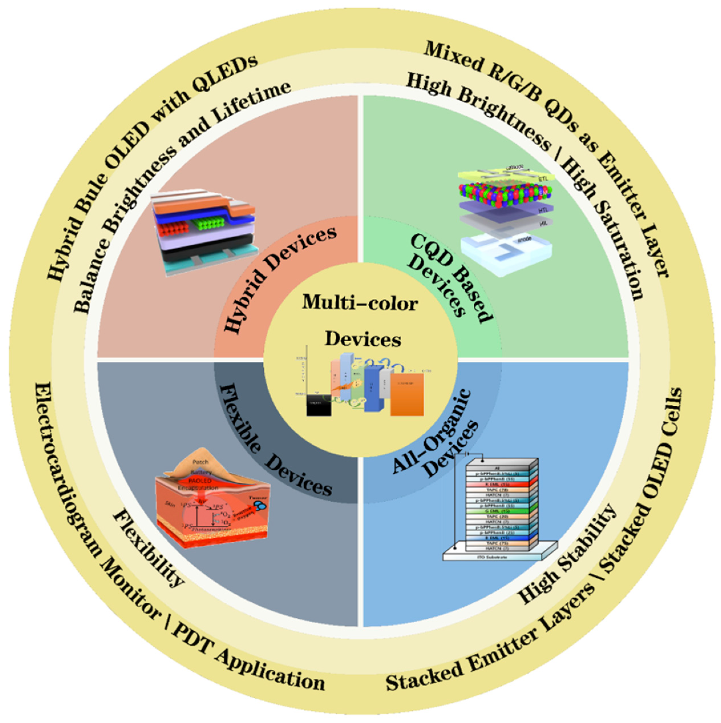
Multi-Color Light-Emitting Diodes


Abstract
1. Introduction
2. Types of Multi-Color Devices
2.1. Multi-Color OLEDs
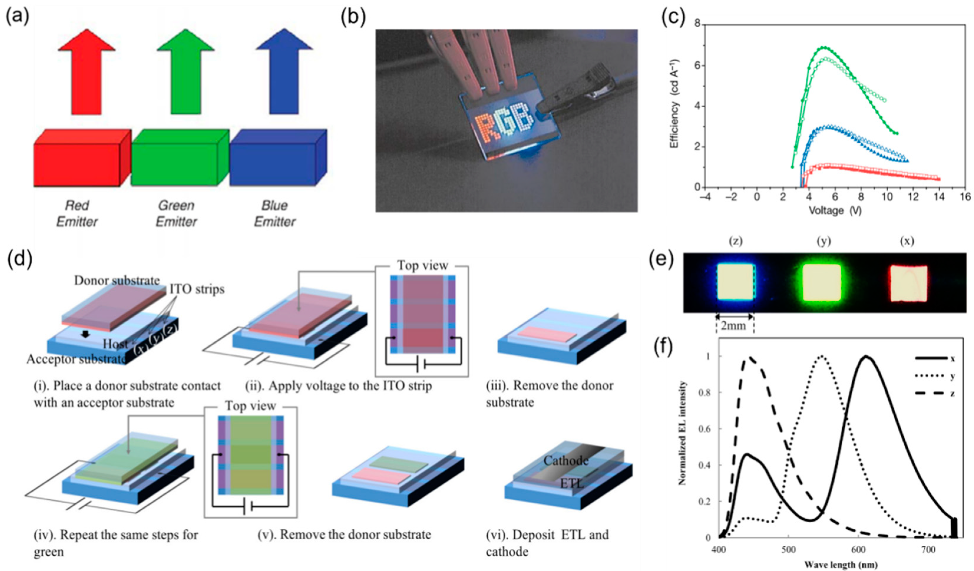
2.1.1. Side-by-Side Structure
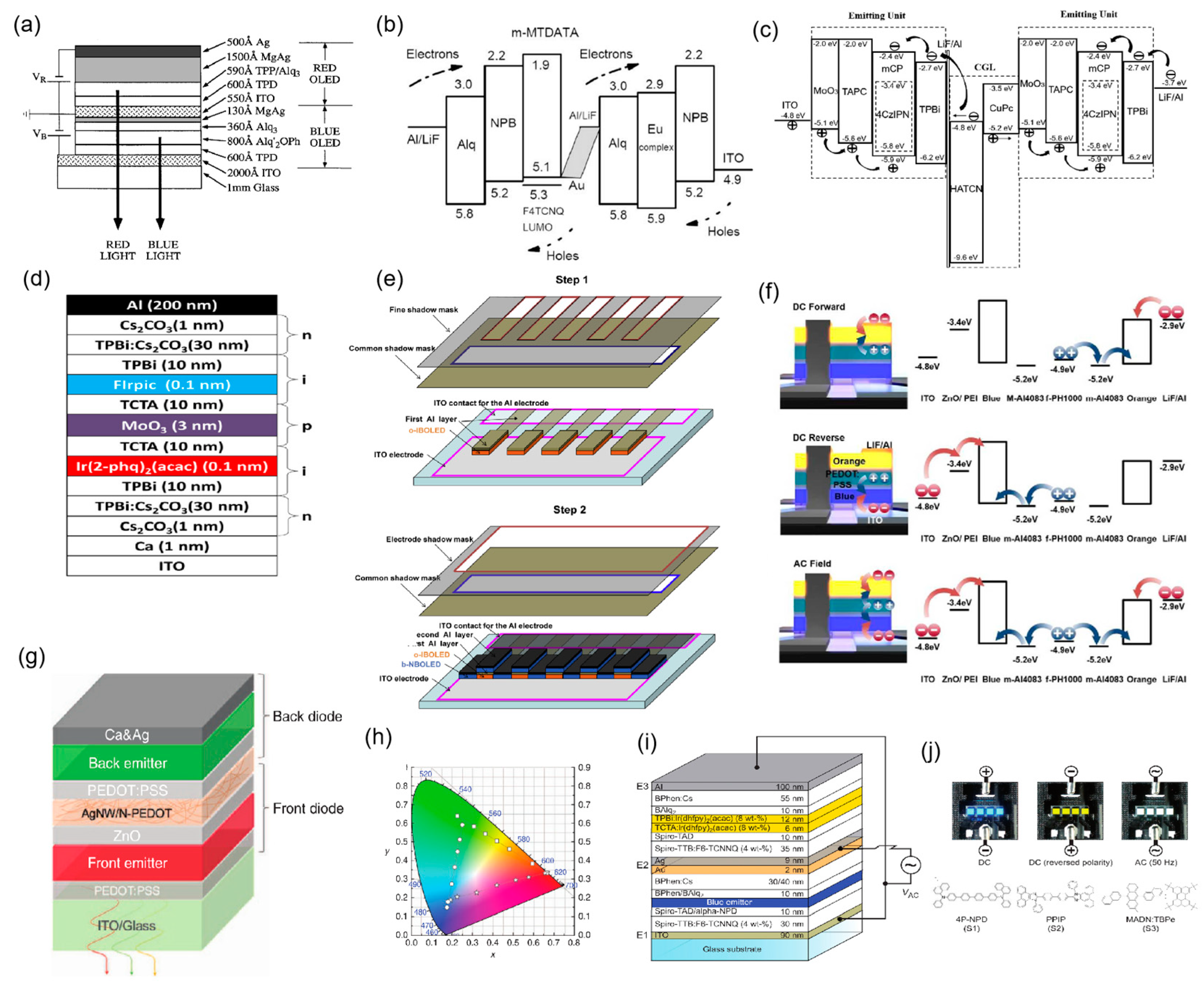
2.1.2. Vertically Stacked OLEDs
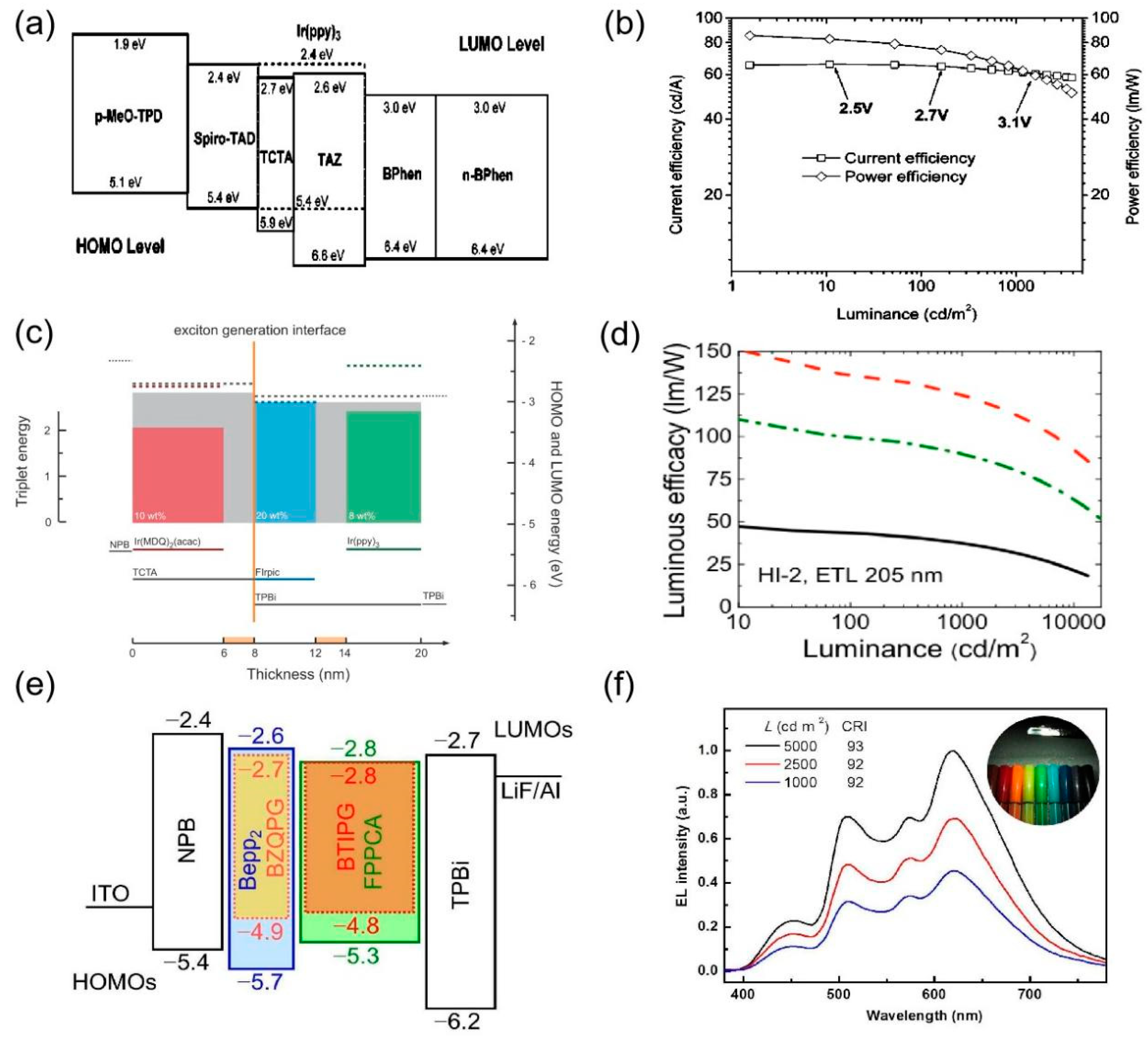
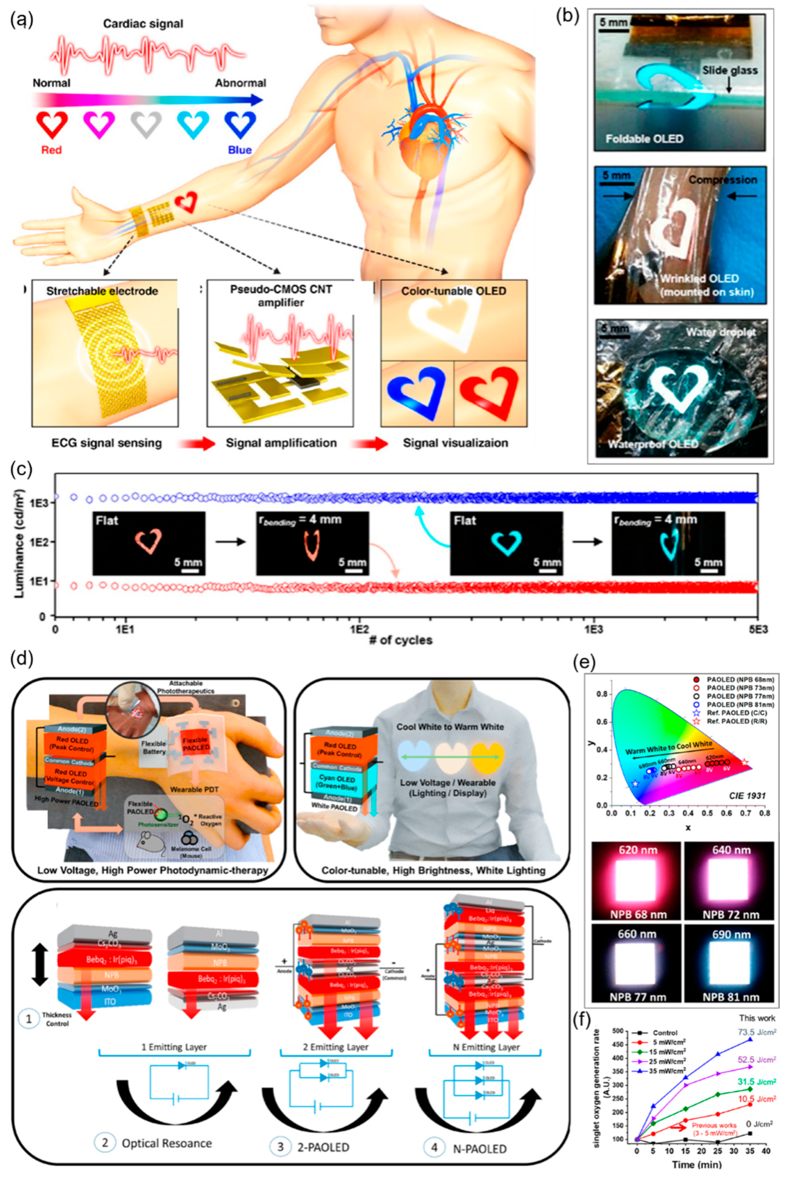
Two-Unit Stacked OLEDs

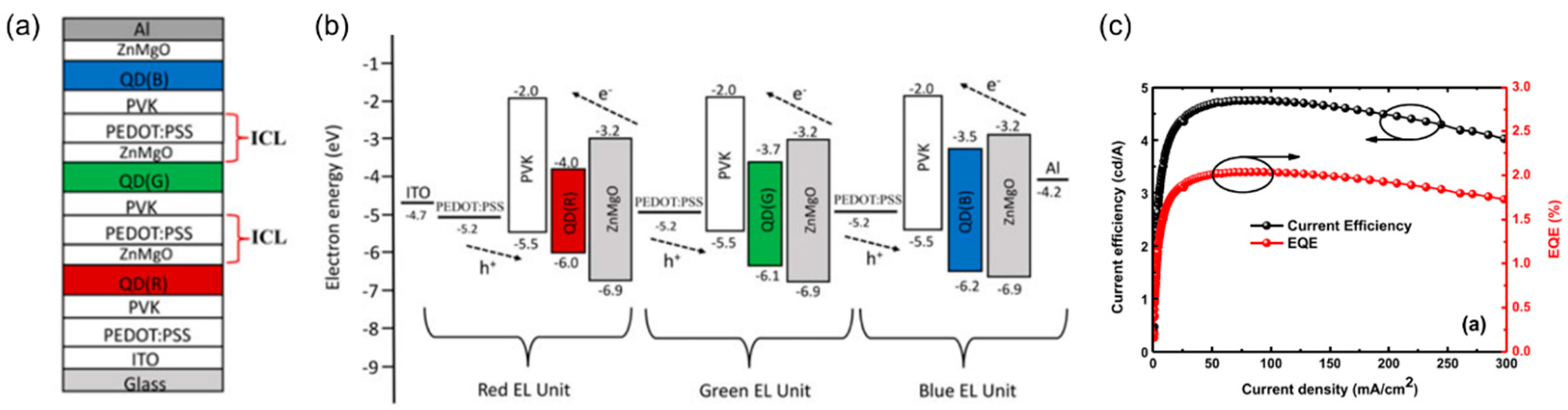
Three-Unit Stacked OLEDs
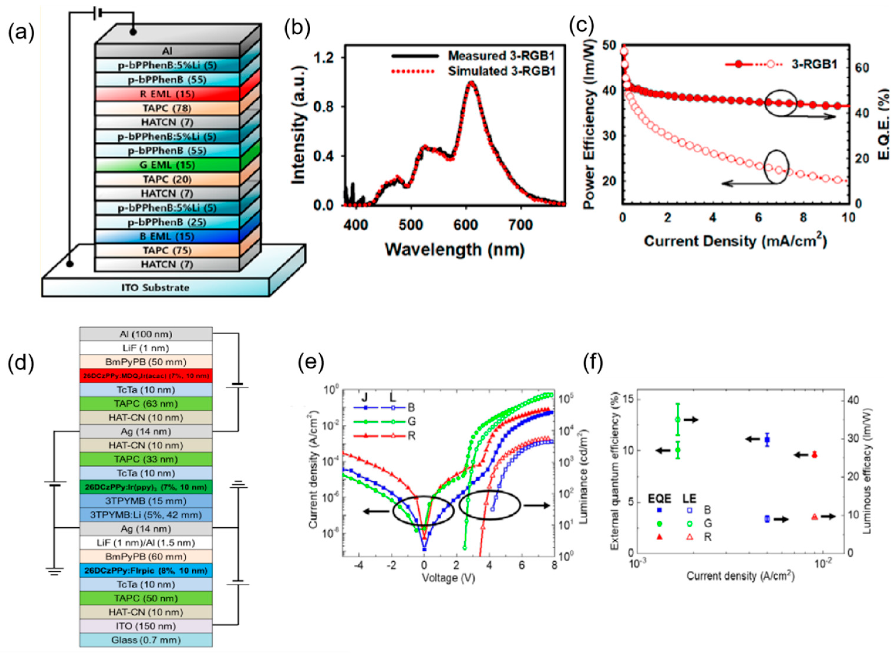
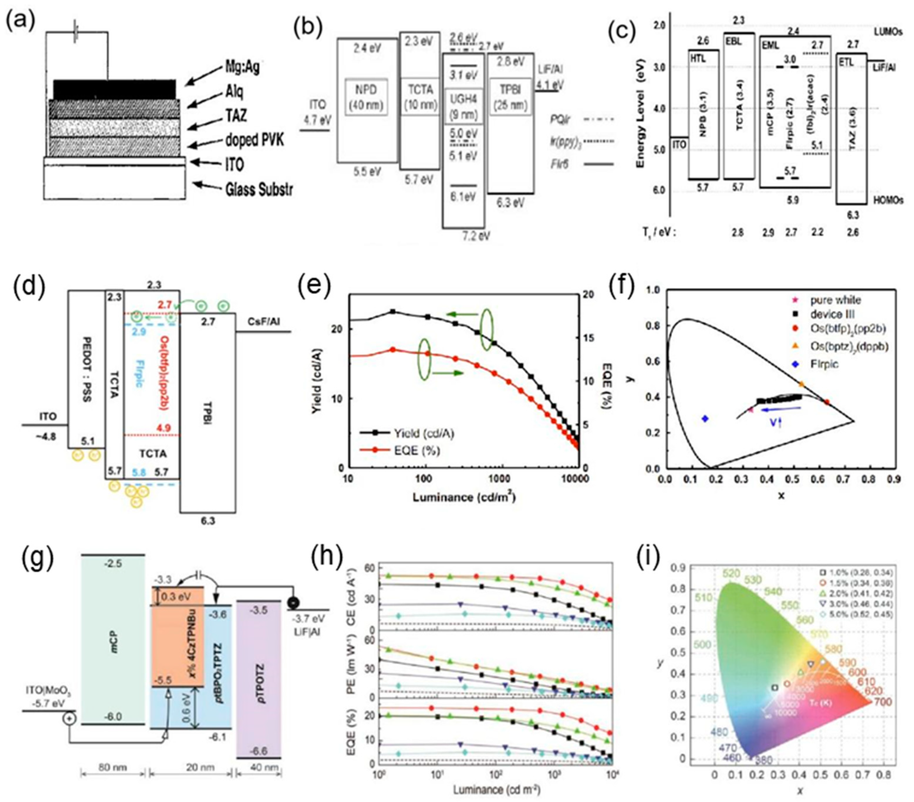
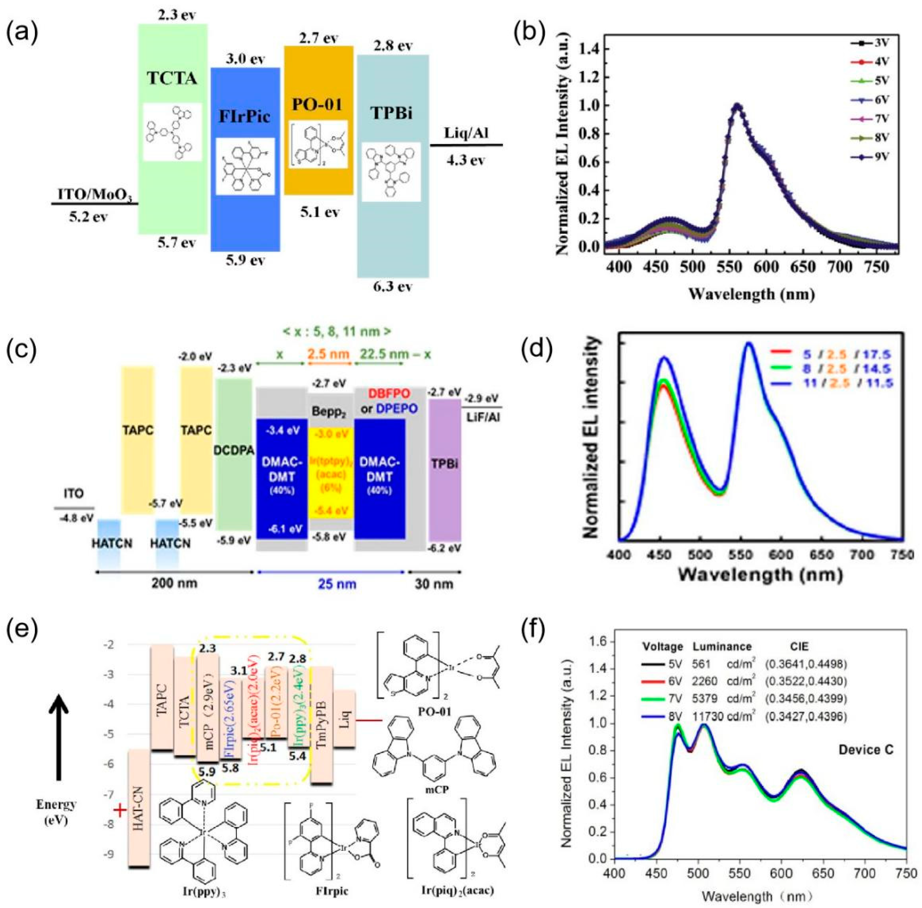
2.1.3. Stacked Emitter Layers
Single Emission Layer
Double Emission Layers
Multiple Emission Layers
2.2. Multi-Color QLEDs
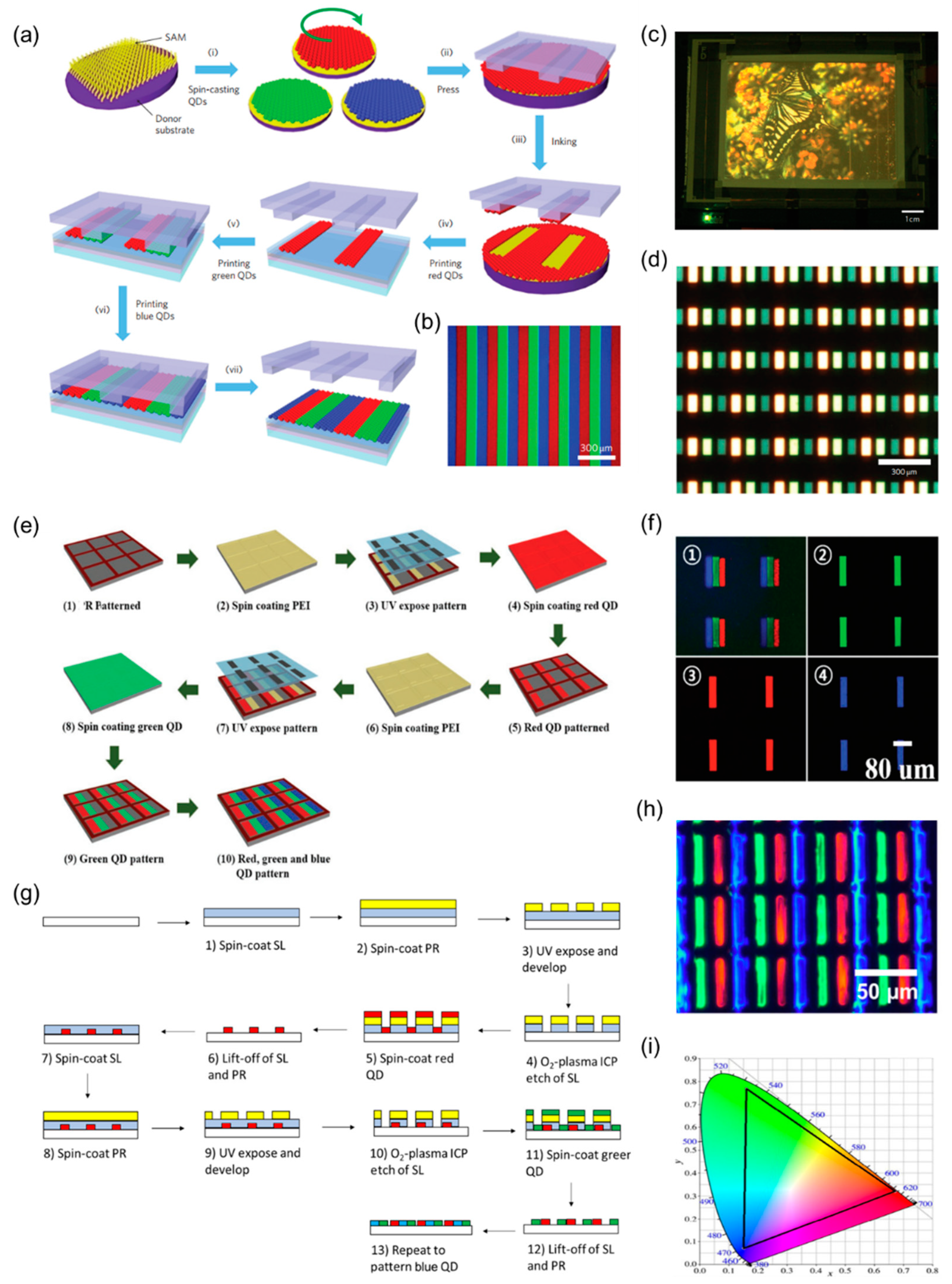
2.2.1. Side-by-Side Structure
2.2.2. Vertically Stacked QLEDs
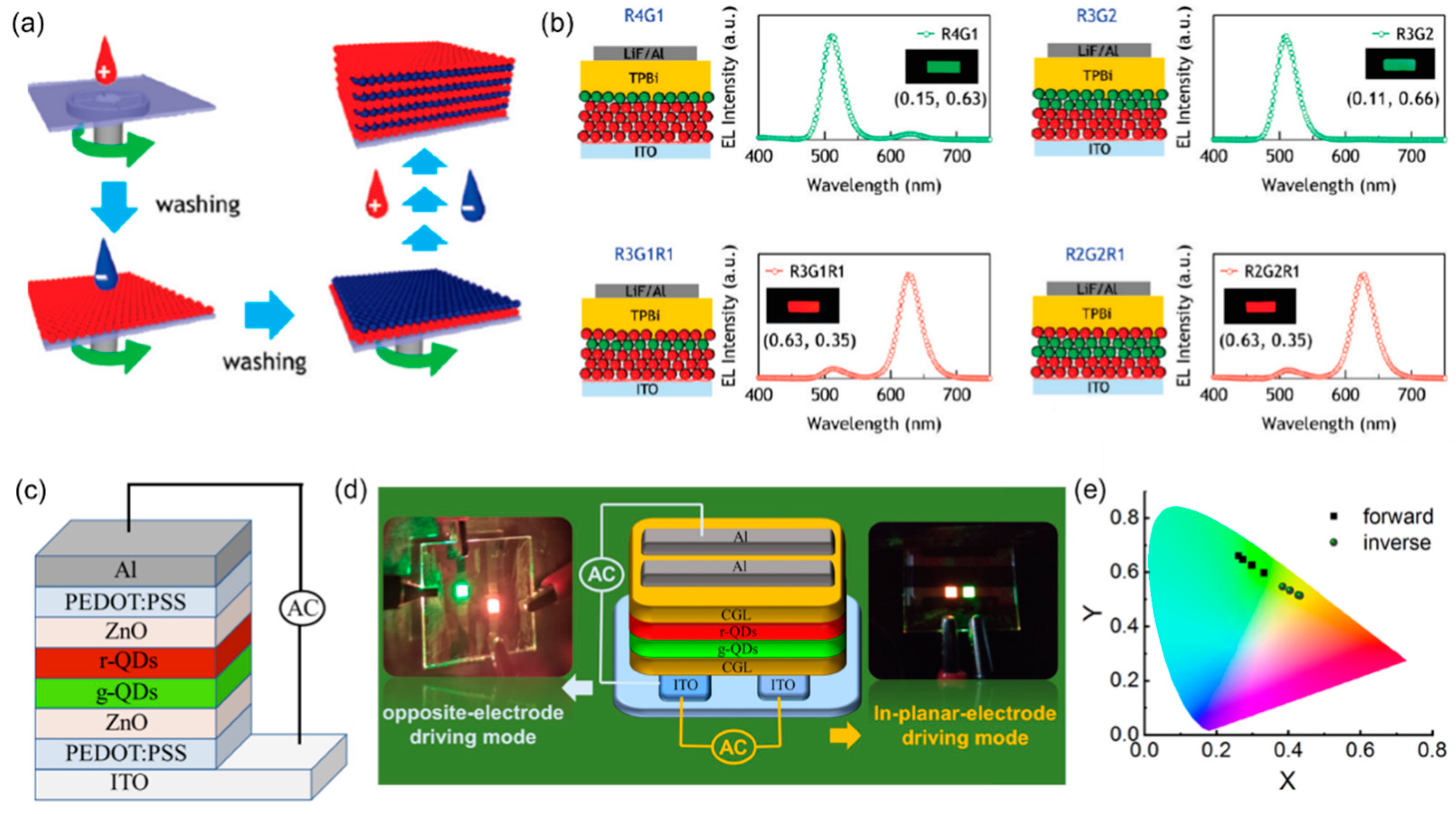
2.2.3. Stacked Emitter Layers
Double or Multiple Emission Layers
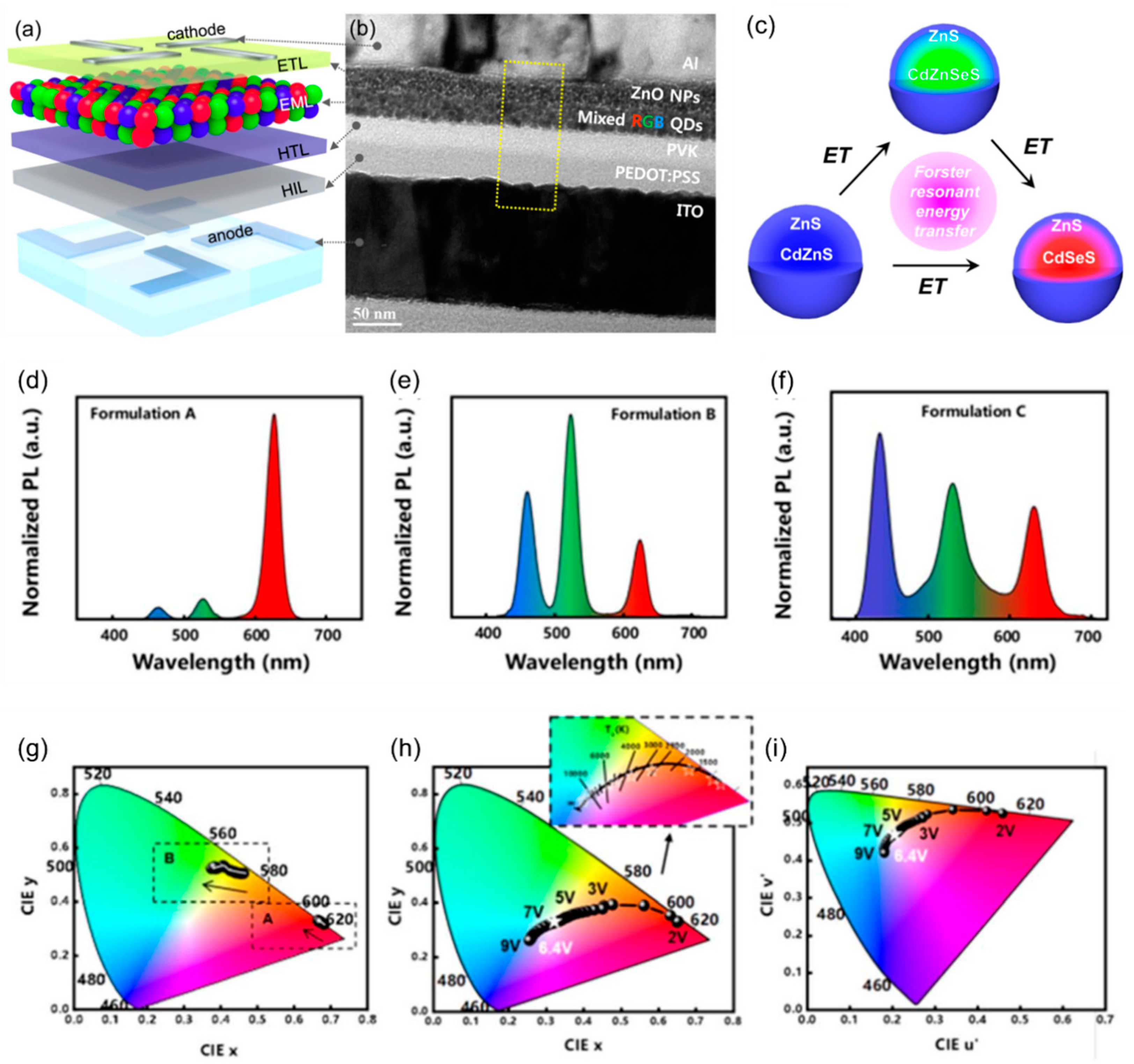
Single Emission Layer with mixed CQDs
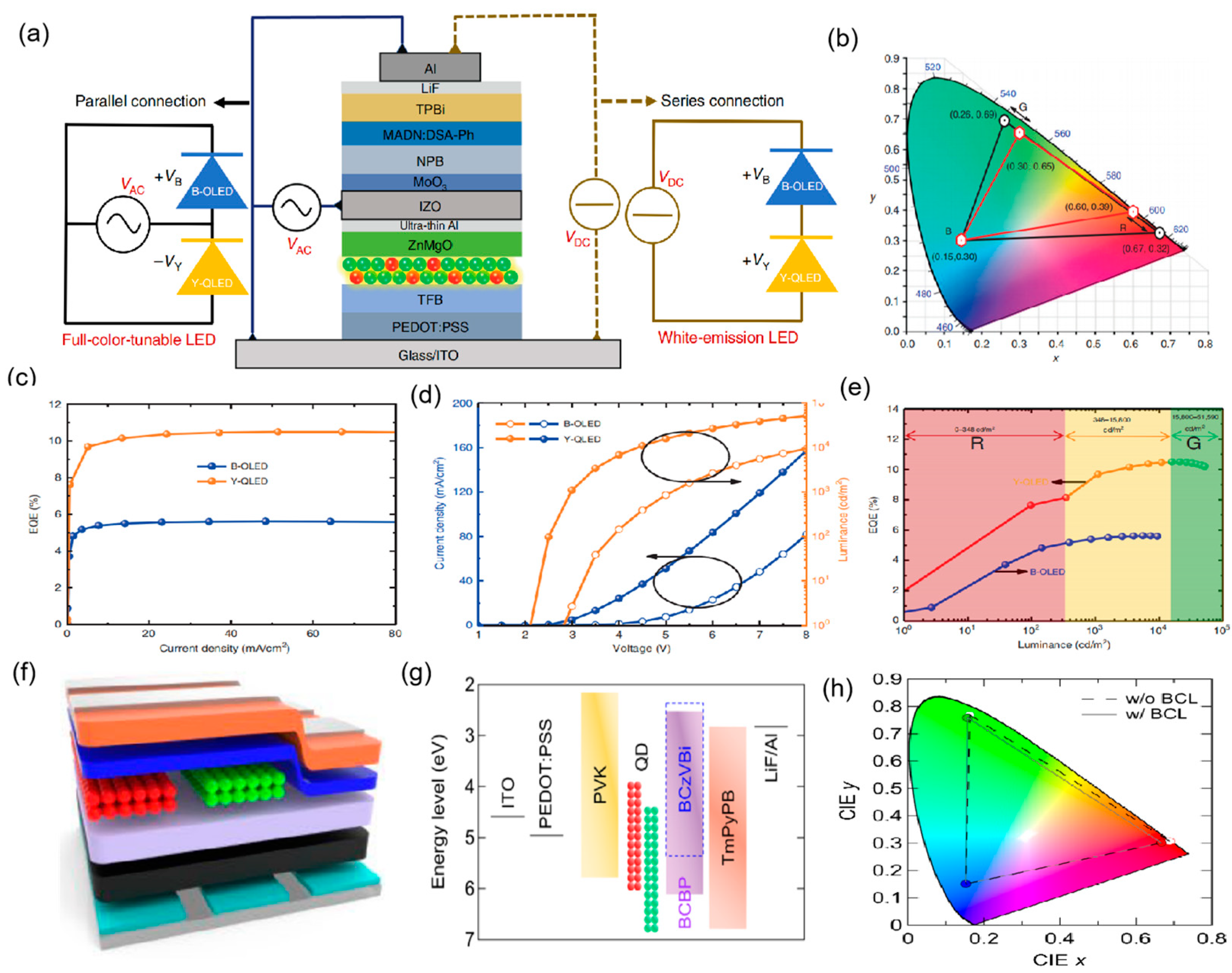
2.3. CQD and Organic Hybrid LED

| Year | Type | Maximum Brightness (cd m−2) | EQE (%) | PE (lm W−1) | CE (cd A−1) | CIE | Ref. | |
|---|---|---|---|---|---|---|---|---|
| 2003 | OLED | Side-by-Side Structure | - | - | - | 7 2.9 | Green blue | [17] |
| 2014 | OLED | Vertically Stacked OLEDs | - | 10.5 | 14.4 | - | - | [83] |
| 2015 | OLED | Vertically Stacked OLEDs | - | 3.4 | 36.8 | - | (0.44, 0.45) | [20] |
| 2016 | OLED | Vertically Stacked OLEDs | 1300 | - | - | 2.5 | (0.326, 0.381) | [68] |
| 2017 | OLED | Vertically Stacked OLEDs | 43,594 | 12.32 | 18.1 | 28.8 | (0.38, 0.44) | [62] |
| 2018 | OLED | Vertically Stacked OLEDs | - | - | 18.1 | - | (0.375, 0.395) | [61] |
| 2018 | OLED | Vertically Stacked OLEDs | - | 49.4 | 33.4 | - | (0.467, 0.423) | [18] |
| 2022 | OLED | Vertically Stacked OLEDs | 5748.4 | 15.1 | 46.3 | 42.9 | (0.247, 0.579) | [67] |
| 2004 | OLED | Single Emission Layer | - | 12 | 42 | - | (0.43, 045) | [70] |
| 2009 | OLED | Single Emission Layer | - | 19.3 | 42.5 | 52.8 | (0.33, 0.39) | [71] |
| 2015 | OLED | Single Emission Layer | - | 13.6 | 14.5 | 22.5 | (0.36, 0.38) | [72] |
| 2020 | OLED | Single Emission Layer | 30,000 | 23.6 | 55.1 | 52.7 | (0.34, 0.36) | [73] |
| 2004 | OLED | Double Emission Layers | - | 19.3 | 64 | - | - | [75] |
| 2010 | OLED | Double Emission Layers | - | 34 | 90 | - | (0.45, 0.47) | [76] |
| 2016 | OLED | Double Emission Layers | - | 23.3 | 63.2 | - | (0.433, 0.458) | [59] |
| 2016 | OLED | Multiple Emission Layers | 11,000 | - | 40.8 | 39.8 | (0.32, 0.39) | [60] |
| 2018 | OLED | Multiple Emission Layers | - | 23.1 | 59.0 | - | (0.324, 0.337) | [77] |
| 2019 | OLED | Multiple Emission Layers | 23,730 | - | 33.42 | 32.74 | (0.391, 0.471) | [63] |
| 2020 | QLED | Side-by-Side Structure | 247,000 | 22.9 | - | 9.8 | (0.16, 0.77) | [34] |
| 2017 | QLED | Vertically Stacked QLEDs | 4206 | 2.0 | 0.46 | 4.75 | (0.30, 0.44) | [80] |
| 2015 | QLED | Stacked Emitter Layers | 1170 | 0.6 | 0.6 | 0.9 | (0.33, 0.253) | [24] |
| 2022 | QLED | Stacked Emitter Layers | 1000 | 13.3 | - | - | (0.283, 0.305) | [35] |
| 2020 | Hybrid LED | Vertically Stacked Structure | 107,000 | 26.02 | 20.31 | - | (0.34, 0.36) | [37] |
| 2022 | Hybrid LED | Vertically Stacked Structure | 7735 | 8.6 | - | - | (0.67, 0.30) | [36] |
| 2022 | Hybrid LED | Vertically Stacked Structure | 24,911 | 13.7 | - | - | (0.16, 0.76) | [36] |
3. Flexible and Wearable Multi-Color Devices
4. Challenges and Perspectives
Author Contributions
Funding
Institutional Review Board Statement
Informed Consent Statement
Data Availability Statement
Conflicts of Interest
References
- Chang, M.H.; Das, D.; Varde, P.V.; Pecht, M. Light Emitting Diodes Reliability Review. Microelectron. Reliab. 2012, 52, 762–782. [Google Scholar] [CrossRef]
- Wang, R.; Xiang, H.; Chen, J.; Li, Y.; Zhou, Y.; Choy, W.C.H.; Fan, Z.; Zeng, H. Energy Regulation in White-Light-Emitting Diodes. ACS Energy Lett. 2022, 7, 2173–2188. [Google Scholar] [CrossRef]
- Wu, Y.; Ma, J.; Su, P.; Zhang, L.; Xia, B. Full-Color Realization of Micro-Led Displays. Nanomaterials 2020, 10, 2482. [Google Scholar] [CrossRef]
- Huang, Y.; Hsiang, E.L.; Deng, M.Y.; Wu, S.T. Mini-LED, Micro-LED and OLED Displays: Present Status and Future Perspectives. Light Sci. Appl. 2020, 9, 105. [Google Scholar] [CrossRef] [PubMed]
- Ma, L.; Shao, Y.F. A brief review of innovative strategies towards structure design of practical electronic display device. J. Cent. South Univ. 2022, 27, 1624–1644. [Google Scholar] [CrossRef]
- Koo, J.H.; Jeong, S.; Shim, H.J.; Son, D.; Kim, J.; Kim, D.C.; Choi, S.; Hong, J.I.; Kim, D.H. Wearable Electrocardiogram Monitor Using Carbon Nanotube Electronics and Color-Tunable Organic Light-Emitting Diodes. ACS Nano 2017, 11, 10032–10041. [Google Scholar] [CrossRef] [PubMed]
- Jeon, Y.; Noh, I.; Seo, Y.C.; Han, J.H.; Park, Y.; Cho, E.H.; Choi, K.C. Parallel-Stacked Flexible Organic Light-Emitting Diodes for Wearable Photodynamic Therapeutics and Color-Tunable Optoelectronics. ACS Nano 2020, 14, 15688–15699. [Google Scholar] [CrossRef] [PubMed]
- Mao, M.; Lam, T.L.; To, W.P.; Lao, X.; Liu, W.; Xu, S.; Cheng, G.; Che, C.M. Stable, High-Efficiency Voltage-Dependent Color-Tunable Organic Light-Emitting Diodes with a Single Tetradentate Platinum(II) Emitter Having Long Operational Lifetime. Adv. Mater. 2021, 33, e2004873. [Google Scholar] [CrossRef] [PubMed]
- Liang, C.J.; Choy, W.C.H. Tunable Full-Color Emission of Two-Unit Stacked Organic Light Emitting Diodes with Dual-Metal Intermediate Electrode. J. Organomet. Chem. 2009, 694, 2712–2716. [Google Scholar] [CrossRef]
- Nakamura, K.; Ishikawa, T.; Nishioka, D.; Ushikubo, T.; Kobayashi, N. Color-Tunable Multilayer Organic Light Emitting Diode Composed of DNA Complex and Tris(8-Hydroxyquinolinato)Aluminum. Appl. Phys. Lett. 2010, 97, 95–98. [Google Scholar] [CrossRef]
- Tsuzuki, T.; Tokito, S. Highly Efficient, Low-Voltage Phosphorescent Organic Light-Emitting Diodes Using an Iridium Complex as the Host Material. Adv. Mater. 2007, 19, 276–280. [Google Scholar] [CrossRef]
- Jiang, Y.; Lian, J.; Chen, S.; Kwok, H.S. Fabrication of Color Tunable Organic Light-Emitting Diodes by an Alignment Free Mask Patterning Method. Org. Electron. 2013, 14, 2001–2006. [Google Scholar] [CrossRef]
- Geffroy, B.; le Roy, P.; Prat, C. Organic Light-Emitting Diode (OLED) Technology: Materials, Devices and Display Technologies. Polym. Int. 2006, 55, 572–582. [Google Scholar] [CrossRef]
- Gayral, B. LEDs for Lighting: Basic Physics and Prospects for Energy Savings. Comptes Rendus Phys. 2017, 18, 453–461. [Google Scholar] [CrossRef]
- Kanno, H.; Hamada, Y.; Takahashi, H. Development of OLED with High Stability and Luminance Efficiency by Co-Doping Methods for Full Color Displays. IEEE J. Sel. Top. Quantum Electron. 2004, 10, 30–36. [Google Scholar] [CrossRef]
- Schwartz, G.; Reineke, S.; Rosenow, T.C.; Walzer, K.; Leo, K. Triplet Harvesting in Hybrid White Organic Light-Emitting Diodes. Adv. Funct. Mater. 2009, 19, 1319–1333. [Google Scholar] [CrossRef]
- Müller, C.D.; Falcou, A.; Reckefuss, N.; Rojahn, M.; Wiederhirn, V.; Rudati, P.; Frohne, H.; Nuyken, O.; Becker, H.; Meerholz, K. Multi-Colour Organic Light-Emitting Displays by Solution Processing. Nature 2003, 421, 829–833. [Google Scholar] [CrossRef]
- Park, M.J.; Son, Y.H.; Yang, H.I.; Kim, S.K.; Lampande, R.; Kwon, J.H. Optical Design and Optimization of Highly Efficient Sunlight-like Three-Stacked Warm White Organic Light Emitting Diodes. ACS Photonics 2018, 5, 655–662. [Google Scholar] [CrossRef]
- Guo, F.; Karl, A.; Xue, Q.F.; Tam, K.C.; Forberich, K.; Brabec, C.J. The Fabrication of Color-Tunable Organic Light-Emitting Diode Displays via Solution Processing. Light Sci. Appl. 2017, 6, e17094. [Google Scholar] [CrossRef]
- Fröbel, M.; Schwab, T.; Kliem, M.; Hofmann, S.; Leo, K.; Gather, M.C. Get It White: Color-Tunable AC/DC OLEDs. Light Sci. Appl. 2015, 4, e247. [Google Scholar] [CrossRef]
- Zhang, J.; Ren, B.; Deng, S.; Huang, J.; Jiang, L.; Zhou, D.; Zhang, X.; Zhang, M.; Chen, R.; Yeung, F.; et al. Voltage-Dependent Multicolor Electroluminescent Device Based on Halide Perovskite and Chalcogenide Quantum-Dots Emitters. Adv. Funct. Mater. 2020, 30, 1907074. [Google Scholar] [CrossRef]
- Zhang, Y.; Xie, C.; Su, H.; Liu, J.; Pickering, S.; Wang, Y.; Yu, W.W.; Wang, J.; Wang, Y.; Hahm, J.I.; et al. Employing Heavy Metal-Free Colloidal Quantum Dots in Solution-Processed White Light-Emitting Diodes. Nano Lett. 2011, 11, 329–332. [Google Scholar] [CrossRef] [PubMed]
- Bae, W.K.; Lim, J.; Lee, D.; Park, M.; Lee, H.; Kwak, J.; Char, K.; Lee, C.; Lee, S. R/G/B/Natural White Light Thin Colloidal Quantum Dot-Based Light-Emitting Devices. Adv. Mater. 2014, 26, 6387–6393. [Google Scholar] [CrossRef]
- Kim, J.H.; Lee, K.H.; Kang, H.D.; Park, B.; Hwang, J.Y.; Jang, H.S.; Do, Y.R.; Yang, H. Fabrication of a White Electroluminescent Device Based on Bilayered Yellow and Blue Quantum Dots. Nanoscale 2015, 7, 5363–5370. [Google Scholar] [CrossRef] [PubMed]
- Wepfer, S.; Frohleiks, J.; Hong, A.R.; Jang, H.S.; Bacher, G.; Nannen, E. Solution-Processed CuInS2-Based White QD-LEDs with Mixed Active Layer Architecture. ACS Appl. Mater. Interfaces 2017, 9, 11224–11230. [Google Scholar] [CrossRef]
- Mu, G.; Rao, T.; Zhang, S.; Wen, C.; Chen, M.; Hao, Q.; Tang, X. Ultrasensitive Colloidal Quantum-Dot Upconverters for Extended Short-Wave Infrared. ACS Appl. Mater. Interfaces 2022, 14, 45553–45561. [Google Scholar] [CrossRef] [PubMed]
- Shen, H.; Gao, Q.; Zhang, Y.; Lin, Y.; Lin, Q.; Li, Z.; Chen, L.; Zeng, Z.; Li, X.; Jia, Y.; et al. Visible quantum dot light-emitting diodes with simultaneous high brightness and efficiency. Nature Photon 2019, 13, 192–197. [Google Scholar] [CrossRef]
- Qasim, K.; Zhenbo, Z.; Khatri, N.K.; Xu, Q.; Subramanian, A.; Qing, L.; Wei, L. A Color Tunable Quantum-Dot Light-Emitting Diode Device Driven by Variable Voltage. J. Nanosci. Nanotechnol. 2018, 19, 1038–1043. [Google Scholar] [CrossRef]
- Wang, O.; Wang, L.; Li, Z.; Xu, Q.; Lin, Q.; Wang, H.; Du, Z.; Shen, H.; Li, L.S. High-Efficiency, Deep Blue ZnCdS/Cd: XZn1- XS/ZnS Quantum-Dot-Light-Emitting Devices with an EQE Exceeding 18%. Nanoscale 2018, 10, 5650–5657. [Google Scholar] [CrossRef]
- Li, X.; Lin, Q.; Song, J.; Shen, H.; Zhang, H.; Li, L.S.; Li, X.; Du, Z. Quantum-Dot Light-Emitting Diodes for Outdoor Displays with High Stability at High Brightness. Adv. Opt. Mater. 2020, 8, 1901145. [Google Scholar] [CrossRef]
- Cao, W.; Xiang, C.; Yang, Y.; Chen, Q.; Chen, L.; Yan, X.; Qian, L. Highly Stable QLEDs with Improved Hole Injection via Quantum Dot Structure Tailoring. Nat. Commun. 2018, 9, 2608. [Google Scholar] [CrossRef] [PubMed]
- Kang, H.L.; Kang, J.; Won, J.K.; Jung, S.M.; Kim, J.; Park, C.H.; Ju, B.K.; Kim, M.G.; Park, S.K. Spatial Light Patterning of Full Color Quantum Dot Displays Enabled by Locally Controlled Surface Tailoring. Adv. Opt. Mater. 2018, 6, 1701335. [Google Scholar] [CrossRef]
- Lee, K.H.; Han, C.Y.; Kang, H.D.; Ko, H.; Lee, C.; Lee, J.; Myoung, N.S.; Yim, S.Y.; Yang, H. Highly Efficient, Color-Reproducible Full-Color Electroluminescent Devices Based on Red/Green/Blue Quantum Dot-Mixed Multilayer. ACS Nano 2015, 9, 10941–10949. [Google Scholar] [CrossRef] [PubMed]
- Mei, W.; Zhang, Z.; Zhang, A.; Li, D.; Zhang, X.; Wang, H.; Chen, Z.; Li, Y.; Li, X.; Xu, X. High-Resolution, Full-Color Quantum Dot Light-Emitting Diode Display Fabricated via Photolithography Approach. Nano Res. 2020, 13, 2485–2491. [Google Scholar] [CrossRef]
- Mu, G.; Rao, T.; Chen, M.; Tan, Y.; Hao, Q.; Hao, Q.; Tang, X. Colloidal Quantum-Dot Light Emitting Diodes with Bias-Tunable Color. Photonics Res. 2022, 10, 1633–1639. [Google Scholar] [CrossRef]
- Lee, S.; Hahm, D.; Yoon, S.Y.; Yang, H.; Bae, W.K.; Kwak, J. Quantum-Dot and Organic Hybrid Light-Emitting Diodes Employing a Blue Common Layer for Simple Fabrication of Full-Color Displays. Nano Res. 2022, 15, 6477–6482. [Google Scholar] [CrossRef]
- Zhang, H.; Su, Q.; Chen, S. Quantum-Dot and Organic Hybrid Tandem Light-Emitting Diodes with Multi-Functionality of Full-Color-Tunability and White-Light-Emission. Nat. Commun. 2020, 11, 2826–2833. [Google Scholar] [CrossRef]
- Wood, V.; Bulović, V. Colloidal Quantum Dot Light-Emitting Devices. Nano Rev. 2010, 1, 5202. [Google Scholar] [CrossRef]
- Hong, G.; Gan, X.; Leonhardt, C.; Zhang, Z.; Seibert, J.; Busch, J.M.; Bräse, S. A Brief History of OLEDs—Emitter Development and Industry Milestones. Adv. Mater. 2021, 33, e2005630. [Google Scholar] [CrossRef]
- Pode, R. Organic Light Emitting Diode Devices: An Energy Efficient Solid State Lighting for Applications. Renew. Sustain. Energy Rev. 2020, 133, 110043. [Google Scholar] [CrossRef]
- Marcato, T.; Shih, C.J. Molecular Orientation Effects in Organic Light-Emitting Diodes. Helv. Chim. Acta 2019, 102, e1900048. [Google Scholar] [CrossRef]
- Ingram, G.L.; Lu, Z.-H. Design Principles for Highly Efficient Organic Light-Emitting Diodes. J. Photonics Energy 2014, 4, 040993. [Google Scholar] [CrossRef]
- Shao, J.; Chen, C.; Zhao, W.; Zhang, E.; Ma, W.; Sun, Y.; Chen, P.; Sheng, R. Recent Advances of Interface Exciplex in Organic Light-Emitting Diodes. Micromachines 2022, 13, 298. [Google Scholar] [CrossRef] [PubMed]
- Qasim, K.; Lei, W.; Li, Q. Quantum Dots for Light Emitting Diodes. J. Nanosci. Nanotechnol. 2013, 13, 3173–3185. [Google Scholar] [CrossRef] [PubMed]
- Seok, H.J.; Lee, J.H.; Park, J.H.; Lim, S.H.; Kim, H.K. Transparent Conducting Electrodes for Quantum Dots Light Emitting Diodes. Isr. J. Chem. 2019, 59, 729–746. [Google Scholar] [CrossRef]
- Fukagawa, H. Molecular Design and Device Design to Improve Stabilities of Organic Light-Emitting Diodes. J. Photopolym. Sci. Technol. 2018, 31, 315–321. [Google Scholar] [CrossRef]
- Vidyasagar, C.C.; Muñoz Flores, B.M.; Jiménez-Pérez, V.M.; Gurubasavaraj, P.M. Recent Advances in Boron-Based Schiff Base Derivatives for Organic Light-Emitting Diodes. Mater. Today Chem. 2019, 11, 133–155. [Google Scholar] [CrossRef]
- Sasabe, H.; Kido, J. Recent Progress in Phosphorescent Organic Light-Emitting Devices. Eur. J. Org. Chem. 2013, 2013, 7653–7663. [Google Scholar] [CrossRef]
- Jeong, H.; Shin, H.; Lee, J.; Kim, B.; Park, Y.-I.; Yook, K.S.; An, B.-K.; Park, J. Recent Progress in the Use of Fluorescent and Phosphorescent Organic Compounds for Organic Light-Emitting Diode Lighting. J. Photonics Energy 2015, 5, 057608. [Google Scholar] [CrossRef]
- Shang, Y.; Ning, Z. Colloidal Quantum Dots Surface and Device Structure Engineering for High Performance Light Emitting. Natl. Sci. Rev. 2017, 4, 107–183. [Google Scholar] [CrossRef]
- Xie, B.; Hu, R.; Luo, X. Quantum Dots-Converted Light-Emitting Diodes Packaging for Lighting and Display: Status and Perspectives. J. Electron. Packag. Trans. ASME 2016, 138, 020803. [Google Scholar] [CrossRef]
- Choi, M.K.; Yang, J.; Hyeon, T.; Kim, D.H. Flexible Quantum Dot Light-Emitting Diodes for next-Generation Displays. npj Flex. Electron. 2018, 2, 1–14. [Google Scholar] [CrossRef]
- Shirasaki, Y.; Supran, G.J.; Bawendi, M.G.; Bulović, V. Emergence of Colloidal Quantum-Dot Light-Emitting Technologies. Nat. Photonics 2013, 7, 13–23. [Google Scholar] [CrossRef]
- Chen, F.; Guan, Z.; Tang, A. Nanostructure and Device Architecture Engineering for High-Performance Quantum-Dot Light-Emitting Diodes. J. Mater. Chem. C 2018, 6, 10958–10981. [Google Scholar] [CrossRef]
- Sun, Y.; Jiang, Y.; Sun, X.W.; Zhang, S.; Chen, S. Beyond OLED: Efficient Quantum Dot Light-Emitting Diodes for Display and Lighting Application. Chem. Rec. 2019, 19, 1729–1752. [Google Scholar] [CrossRef]
- Yuan, Q.; Wang, T.; Yu, P.; Zhang, H.; Zhang, H.; Ji, W. A Review on the Electroluminescence Properties of Quantum-Dot Light-Emitting Diodes. Org. Electron. 2021, 90, 106086. [Google Scholar] [CrossRef]
- Niikura, H.; Légaré, F.; Hasbani, R.; Ivanov, M.Y.; Villeneuve, D.M.; Corkum, P.B. Probing Molecular Dynamics with Attosecond Resolution Using Correlated Wave Packet Pairs. Nature 2003, 421, 826–829. [Google Scholar] [CrossRef]
- Wu, S.; Li, S.; Sun, Q.; Huang, C.; Fung, M.K. Highly Efficient White Organic Light-Emitting Diodes with Ultrathin Emissive Layers and a Spacer-Free Structure. Sci. Rep. 2016, 6, 25821. [Google Scholar] [CrossRef]
- Zhuang, X.; Zhang, H.; Ye, K.; Liu, Y.; Wang, Y. Two Host-Dopant Emitting Systems Realizing Four-Color Emission: A Simple and Effective Strategy for Highly Efficient Warm-White Organic Light-Emitting Diodes with High Color-Rendering Index at High Luminance. ACS Appl. Mater. Interfaces 2016, 8, 11221–11225. [Google Scholar] [CrossRef]
- Chen, P.; Chen, B.; Zuo, L.; Duan, Y.; Han, G.; Sheng, R.; Xue, K.; Zhao, Y. High-Efficiency and Superior Color-Stability White Phosphorescent Organic Light-Emitting Diodes Based on Double Mixed-Host Emission Layers. Org. Electron. 2016, 31, 136–141. [Google Scholar] [CrossRef]
- Lee, H.; Cho, H.; Byun, C.-W.; Han, J.-H.; Kwon, B.-H.; Choi, S.; Lee, J.; Cho, N.S. Color-Tunable Organic Light-Emitting Diodes with Vertically Stacked Blue, Green, and Red Colors for Lighting and Display Applications. Opt. Express 2018, 26, 18351. [Google Scholar] [CrossRef] [PubMed]
- Wu, J.Y.; Chen, S.A. Development of a Highly Efficient Hybrid White Organic-Light-Emitting Diode with a Single Emission Layer by Solution Processing. ACS Appl. Mater. Interfaces 2018, 10, 4851–4859. [Google Scholar] [CrossRef] [PubMed]
- Wang, B.; Kou, Z.; Tang, Y.; Yang, F.; Fu, X.; Yuan, Q. High CRI and Stable Spectra White Organic Light-Emitting Diodes with Double Doped Blue Emission Layers and Multiple Ultrathin Phosphorescent Emission Layers by Adjusting the Thickness of Spacer Layer. Org. Electron. 2019, 70, 149–154. [Google Scholar] [CrossRef]
- Kajiyama, Y.; Kajiyama, K.; Aziz, H. Maskless RGB Color Patterning of Vacuum-Deposited Small Molecule OLED Displays by Diffusion of Luminescent Dopant Molecules. Opt. Express 2015, 23, 16650. [Google Scholar] [CrossRef]
- Burrows, P.E.; Forrest, S.R.; Sibley, S.P.; Thompson, M.E. Color-Tunable Organic Light-Emitting Devices. Appl. Phys. Lett. 1996, 69, 2959–2961. [Google Scholar] [CrossRef]
- Zhao, Y.; Chen, R.; Gao, Y.; Leck, K.S.; Yang, X.; Liu, S.; Abiyasa, A.P.; Divayana, Y.; Mutlugun, E.; Tan, S.T.; et al. AC-Driven, Color- and Brightness-Tunable Organic Light-Emitting Diodes Constructed from an Electron Only Device. Org. Electron. 2013, 14, 3195–3200. [Google Scholar] [CrossRef]
- Chang, Q.; Lü, Z.; Yin, Y.; Xiao, J.; Wang, J. Highly Efficient Tandem OLED Based on a Novel Charge Generation Layer of HAT-CN/CuPc Heterojunction. Displays 2022, 75, 102306. [Google Scholar] [CrossRef]
- Cho, S.H.; Kim, E.H.; Jeong, B.; Lee, J.H.; Song, G.; Hwang, I.; Cho, H.; Kim, K.L.; Yu, S.; Kim, R.H.; et al. Solution-Processed Electron-Only Tandem Polymer Light-Emitting Diodes for Broad Wavelength Light Emission. J. Mater. Chem. C 2017, 5, 110–117. [Google Scholar] [CrossRef]
- Kido, J.; Hongawa, K.; Okuyama, K.; Nagai, K. White Light-Emitting Organic Electroluminescent Devices Using the Poly(N-Vinylcarbazole) Emitter Layer Doped with Three Fluorescent Dyes. Appl. Phys. Lett. 1994, 64, 815–817. [Google Scholar] [CrossRef]
- D’Andrade, B.W.; Holmes, R.J.; Forrest, S.R. Efficient Organic Electrophosphorescent White-Light-Emitting Device with a Triple Doped Emissive Layer. Adv. Mater. 2004, 16, 624–628. [Google Scholar] [CrossRef]
- Wang, Q.; Ding, J.; Dongge, M.; Cheng, Y.; Wang, L.; Jing, X.; Wang, F. Harvesting Excitons via Two Parallel Channels for Efficient White Organic LEDs with Nearly 100% Internal Quantum Efficiency: Fabrication and Emission-Mechanism Analysis. Adv. Funct. Mater. 2009, 19, 84–95. [Google Scholar] [CrossRef]
- Huang, M.H.; Lin, W.C.; Fan, C.C.; Wang, Y.S.; Lin, H.W.; Liao, J.L.; Lin, C.H.; Chi, Y. Tunable Chromaticity Stability in Solution-Processed Organic Light Emitting Devices. Org. Electron. 2015, 20, 36–42. [Google Scholar] [CrossRef]
- Ding, D.; Wang, Z.; Li, C.; Zhang, J.; Duan, C.; Wei, Y.; Xu, H. Highly Efficient and Color-Stable Thermally Activated Delayed Fluorescence White Light-Emitting Diodes Featured with Single-Doped Single Emissive Layers. Adv. Mater. 2020, 32, e1906950. [Google Scholar] [CrossRef] [PubMed]
- Zhou, X.; Qin, D.S.; Pfeiffer, M.; Blochwitz-Nimoth, J.; Werner, A.; Drechsel, J.; Maennig, B.; Leo, K.; Bold, M.; Erk, P.; et al. High-Efficiency Electrophosphorescent Organic Light-Emitting Diodes with Double Light-Emitting Layers. Appl. Phys. Lett. 2002, 81, 4070–4072. [Google Scholar] [CrossRef]
- He, G.; Pfeiffer, M.; Leo, K.; Hofmann, M.; Birnstock, J.; Pudzich, R.; Salbeck, J. High-Efficiency and Low-Voltage p-i-n Electrophosphorescent Organic Light-Emitting Diodes with Double-Emission Layers. Appl. Phys. Lett. 2004, 85, 3911–3913. [Google Scholar] [CrossRef]
- Reineke, S.; Lindner, F.; Schwartz, G.; Seidler, N.; Walzer, K.; Lüssem, B.; Leo, K. White Organic Light-Emitting Diodes with Fluorescent Tube Efficiency. Nature. 2009, 459, 234–238. [Google Scholar] [CrossRef]
- Kim, G.W.; Bae, H.W.; Lampande, R.; Ko, I.J.; Park, J.H.; Lee, C.Y.; Kwon, J.H. Highly Efficient Single-Stack Hybrid Cool White OLED Utilizing Blue Thermally Activated Delayed Fluorescent and Yellow Phosphorescent Emitters. Sci. Rep. 2018, 8, 16263. [Google Scholar] [CrossRef]
- Colvin, V.L.; Schlamp, M.C.; Alivisatos, A.P. Light-Emitting Diodes Made from Cadmium Selenide Nanocrystals and a Semiconducting Polymer. Nature 1994, 370, 354–357. [Google Scholar] [CrossRef]
- Kim, T.H.; Cho, K.S.; Lee, E.K.; Lee, S.J.; Chae, J.; Kim, J.W.; Kim, D.H.; Kwon, J.Y.; Amaratunga, G.; Lee, S.Y.; et al. Full-Colour Quantum Dot Displays Fabricated by Transfer Printing. Nat. Photonics 2011, 5, 176–182. [Google Scholar] [CrossRef]
- Zhang, H.; Wang, S.; Sun, X.; Chen, S. All Solution-Processed White Quantum-Dot Light-Emitting Diodes with Three-Unit Tandem Structure. J. Soc. Inf. Disp. 2017, 25, 143–150. [Google Scholar] [CrossRef]
- Ki Bae, W.; Kwak, J.; Lim, J.; Lee, D.; Ki Nam, M.; Char, K.; Lee, C.; Lee, S. Multicolored Light-Emitting Diodes Based on All-Quantum-Dot Multilayer Films Using Layer-by-Layer Assembly Method. Nano Lett. 2010, 10, 2368–2373. [Google Scholar] [CrossRef] [PubMed]
- Wang, T.; Chen, Z.; Zhang, H.; Ji, W. Color-Tunable Alternating-Current Quantum Dot Light-Emitting Devices. ACS Appl. Mater. Interfaces 2021, 13, 45815–45821. [Google Scholar] [CrossRef] [PubMed]
- Joo, C.W.; Moon, J.; Han, J.H.; Huh, J.W.; Lee, J.; Cho, N.S.; Hwang, J.; Chu, H.Y.; Lee, J.I. Color Temperature Tunable White Organic Light-Emitting Diodes. Org. Electron. 2014, 15, 189–195. [Google Scholar] [CrossRef]


Disclaimer/Publisher’s Note: The statements, opinions and data contained in all publications are solely those of the individual author(s) and contributor(s) and not of MDPI and/or the editor(s). MDPI and/or the editor(s) disclaim responsibility for any injury to people or property resulting from any ideas, methods, instructions or products referred to in the content. |
© 2023 by the authors. Licensee MDPI, Basel, Switzerland. This article is an open access article distributed under the terms and conditions of the Creative Commons Attribution (CC BY) license (https://creativecommons.org/licenses/by/4.0/).
Share and Cite
Ma, S.; Qi, Y.; Mu, G.; Chen, M.; Tang, X. Multi-Color Light-Emitting Diodes. Coatings 2023, 13, 182. https://doi.org/10.3390/coatings13010182
Ma S, Qi Y, Mu G, Chen M, Tang X. Multi-Color Light-Emitting Diodes. Coatings. 2023; 13(1):182. https://doi.org/10.3390/coatings13010182
Chicago/Turabian StyleMa, Su, Yawei Qi, Ge Mu, Menglu Chen, and Xin Tang. 2023. "Multi-Color Light-Emitting Diodes" Coatings 13, no. 1: 182. https://doi.org/10.3390/coatings13010182
APA StyleMa, S., Qi, Y., Mu, G., Chen, M., & Tang, X. (2023). Multi-Color Light-Emitting Diodes. Coatings, 13(1), 182. https://doi.org/10.3390/coatings13010182