


Abstract
With the rapid advancement of digital microfluidic technology, this study presents the design and fabrication of a PCB-based digital microfluidic system aimed at reducing chip driving voltage and manufacturing costs while enhancing droplet manipulation performance. The system integrates peripheral modules to establish a complete digital microfluidic platform. A novel double half-moon serrated electrode is proposed, which provides enhanced droplet driving force and enables multidirectional droplet movement through flexible electrode arrangement. Three electrode configurations with different scaling parameters were designed and experimentally evaluated. The results demonstrate that the electrode with a scaling parameter of A = 1 exhibits the best driving performance. At an applied voltage of 120 V, the average droplet velocities in the transverse and longitudinal directions reached 1.18 mm/s and 0.98 mm/s, respectively, while at 200 V they increased to 2.57 mm/s and 1.88 mm/s. Compared with conventional rectangular and serrated electrodes, the proposed electrode structure effectively improves droplet driving capability. This work provides a low-cost and high-performance solution for the development of portable and integrated digital microfluidic systems.
1. Introduction
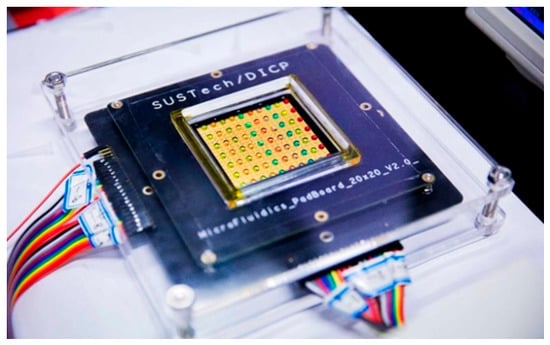
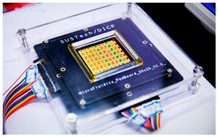
The Digital Microfluidic Biochip (DMFB) is an example of a lab-on-a-chip that utilizes the principle of electrowetting-on-dielectric (EWOD) [1] to automate biochemical experiments [2,3,4]. Digital microfluidic biochips, as shown in Figure 1, use discrete droplets as carriers for a variety of fluidic manipulations, biochemical reactions, and biological assays on a microscopic scale. Compared with traditional microfluidic biochips based on continuous fluids, the main advantages are (1) lower cost, power consumption, and higher system integration; (2) multiple droplets can be controlled simultaneously on a large-scale chip for parallel operations, such as splitting and mixing; and (3) addressable electrodes on the chip can be reconfigured into multiple microfluidic modules.
Figure 1.
Digital microfluidic chip.
Over the last decade, digital microfluidic biochips have been used for high-throughput DNA sequencing [5,6], clinical diagnostics [7,8], and protein crystallization for drug discovery [9,10,11]. Tom Kasputis et al. [12] developed a digital microfluidic biochip for detecting emerging pathogens, while Jon Washburn et al. [13] discussed the progress of applying DMF to newborn screening for diseases in the United States. These successful applications highlight the versatility of digital microfluidic technology. With the integration of different types of sensors, such as capacitive and optical sensors, the chip enables real-time feedback and software control, further enhancing the attractiveness of digital microfluidic platforms.
In digital microfluidic systems, there are various driving methods for manipulating droplets, such as electrowetting-on-dielectric (EWOD) [14,15], dielectric electrophoresis [16,17], light-induced driving [18,19], surface acoustic wave [20,21], and light-driven electrowetting methods [22,23]. These driving mechanisms differ substantially in their actuation principles, device architectures, fabrication requirements, and control strategies. Dielectrophoretic actuation can provide precise manipulation of droplets and particles through non-uniform electric fields but generally requires specific electrode configurations and careful control of the electric field distribution [16,17]. Light-induced and optically controlled approaches provide flexible and reconfigurable actuation, but their implementation usually requires additional optical components and relatively complex light-addressing system. Surface acoustic wave (SAW)-based systems can achieve rapid droplet manipulation and have been widely investigated for mixing and transport applications; however, they require acoustic transducers and corresponding high-frequency excitation circuits, which can increase system complexity. In contrast, EWOD manipulates droplets directly through electrically induced changes in the interfacial wettability of a dielectric-coated electrode, allowing droplet transport, dispensing, merging, mixing, and splitting to be achieved using individually addressable electrodes.
EWOD is therefore considered a particularly promising actuation mechanism for DMF systems because of its relatively simple planar structure, direct electrical addressing, and compatibility with programmable control. A typical EWOD device consists of an electrode layer, dielectric layer, and hydrophobic surface without requiring mechanical moving components or additional optical or acoustic actuation elements. By selectively applying voltages to neighboring electrodes, the electrowetting-induced change in the droplet contact angle generates a driving force, enabling the droplet to be transported along a predefined electrode sequence. This electrical addressing scheme is highly compatible with integrated electronic control circuits, allowing the actuation process to be readily automated and reconfigured. In addition, the planar electrode architecture facilitates electrode array scaling and integration with sensing, signal-processing, and communication modules, which is advantageous for developing compact and multifunctional digital microfluidic platforms.
Another important advantage of EWOD for the present study is its compatibility with low-cost and flexible fabrication strategies. Because droplet actuation is primarily determined by the geometry and electrical features of the electrode array together with the dielectric and hydrophobic layers, the electrode structure can be modified without fundamentally changing the overall actuation architecture. This provides a convenient platform for investigating the relationship between electrode geometry, effective three-phase contact line length, driving force, and droplet velocity. Compared with optical or acoustic actuation methods, EWOD can also be implemented using conventional electronic driving circuits and PCB-based electrode structures, making it particularly suitable for a compact, modular, and cost-effective DMF system.
Based on these considerations, EWOD was selected as the actuation mechanism in this study. The selection is not based solely on its droplet driving capability but also on its compatibility with the research objectives of electrode structure optimization and PCB-based system integration. Specifically, the electrically addressable electrode array provides a direct means of modifying the electrode geometry while maintaining the same driving principle and control architecture. This enables the influence of electrode shape on droplet actuation to be experimentally investigated under comparable operating conditions. Meanwhile, the relatively simple electrical actuation architecture facilitates the integration of the DMF chip with the driving circuit and the control module, which is consistent with the objective of developing a simple, convenient, low-cost, and easily controllable digital microfluidic platform.
For EWOD-based DMF systems, reducing the droplet driving voltage while maintaining or improving actuation efficiency remains an important research issue. When the voltage applied to the droplet is too high, a strong electric field is formed in the digital microfluidic chip, which is prone to causing irreversible damages to the active substances contained in the droplet [24,25]. Moreover, excessive driving voltage may increase dielectric stress, leakage current, and the risk of dielectric breakdown, thereby affecting the long-term reliability of the DMF device. Consequently, reducing the required actuation voltage while maintaining sufficient droplet driving force is important for improving the safety, reliability, and practical applicability of EWOD-based systems.
There are two ways to reduce the voltage: (1) the use of materials with high dielectric constants for the dielectric layer [26,27]; (2) optimization of the electrode shape [28,29,30]. Compared with changing the dielectric material, electrode geometry optimization provides a relatively direct approach to modifying the electric field distribution and the effective three-phase contact line while retaining the basic dielectric and hydrophobic materials. It can therefore improve droplet actuation without substantially increasing the complexity of the overall chip structure.
As for electrode shapes, the most common shapes are rectangular [31], and the electrode shapes proposed to improve the droplet driving ability are serrated [32] and half-moon shape [33]. All of these electrodes are effective in improving droplet actuation, but, overall, the shape of the electrodes can be further optimized to improve the performance of actuated droplets. In particular, the geometry of the electrode edge directly affects the effective three-phase contact line and the distribution of the electrowetting-induced driving force. Serrated electrodes can increase effective contact line interaction, whereas half-moon electrodes provide a curved electrode boundary that can improve the interaction between the activated electrode and the droplet. However, existing electrode configurations generally emphasize either enhanced driving capability or structural simplicity. A suitable electrode geometry that combines an enlarged effective contact line with convenient array arrangement remains worthy of further investigation.
In this paper, starting from improving the driving efficiency of the droplets on the array electrodes and reducing the driving voltage, we design the hardware system, build the digital microfluidic platform, design different shapes of electrodes, and study the performance of the digital microfluidic chip for driving electrodes to reduce the driving voltage through experimental verification.
To address these issues, this study proposes and experimentally investigates a double half-moon serrated electrode structure for EWOD-based digital microfluidics. The proposed geometry combines the curved characteristics of half-moon electrodes with the edge features of serrated electrodes, aiming to increase the effective three-phase contact line interaction while maintaining a convenient electrode array configuration. The effects of the structural parameters of the proposed electrode on droplet actuation are systematically analyzed, and the droplet driving performance is experimentally evaluated at different applied voltages.
- A double half-moon serrated electrode is proposed, which can provide both strong droplet driving ability and a convenient combination arrangement.
- Analyze the effect on the effective three-phase contact line of the droplet by changing the double half-moon serrated electrode with different structural parameters and experimentally verify that the electrode shape can effectively reduce the driving voltage in order to drive the droplet.
- Using 5CST silicone oil as the hydrophobic layer and plastic wrap as the dielectric layer ensures both usability and practicality while effectively reducing production costs.
- Design and fabricate a PCB-based digital microfluidic platform with the advantages of simplicity, convenience, low cost, and easy control.
2. Theoretical Research
2.1. Dielectric Wetting Fundamentals
In nature, when a droplet is placed on the surface of a solid, the droplet spreads along the contact surface with the solid under the action of surface tension, which in turn produces surface wetting [34,35]. However, because the electrically wetted droplet is in direct contact with the electrode, if a relatively large voltage applied to the electrode is given, the droplet is easily electrolyzed, and it is not possible to drive the droplet to move at the same time, damage may be caused to the electrode. And, this phenomenon of adding a dielectric layer between the droplet and the electrode, where droplet wetting can occur, is called dielectric wetting.
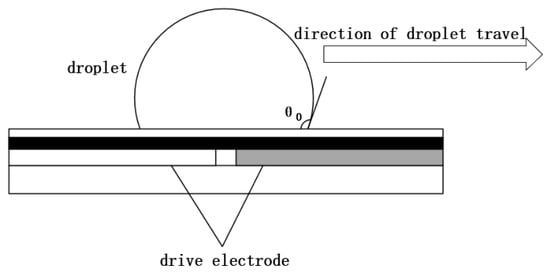
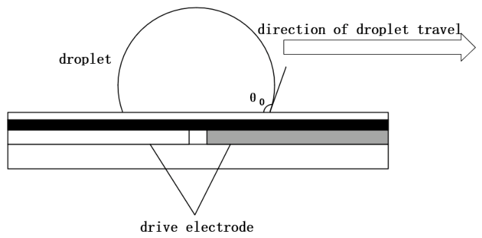
The dielectric wetting process is shown in Figure 2, where the droplets are located on top of the left and right electrodes and the front part of the droplets is located on top of the left drive electrode. When the left drive electrode is energized, the wettability of the surface at the interface between the microdroplet and the driving electrode changes with the applied voltage, causing the surface to transition from a hydrophobic state to a more hydrophilic state. The relationship between driving voltage and contact angle can be described by the Young–Lippmann equation [36], as shown in Equation (1):
Figure 2.
Dielectric wettability.
In Equation (1), θv and θ0 are the initial contact angle without driving voltage and the contact angle with driving voltage, respectively. εr is the relative permittivity of the dielectric layer, ε0 is the vacuum permittivity, γLG is the “liquid-gas” surface tension, V is the applied voltage, and δ is the thickness of the dielectric layer. As indicated by Equation (1), increasing the applied driving voltage leads to a reduction in the contact angle of the microdroplet.
2.2. Electrode Principle Analysis
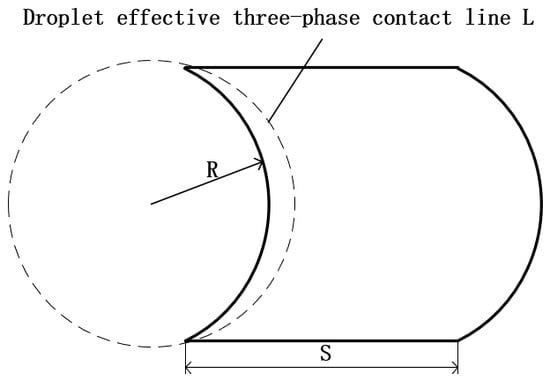
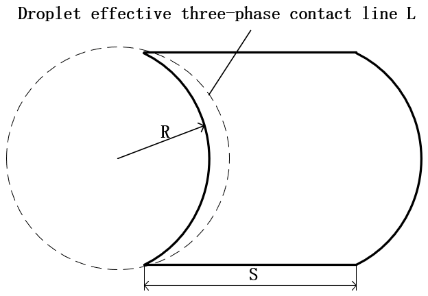
The design of the crescent shaped drive electrode is effective in reducing the drive voltage of the chip compared to square- and sawtooth-shaped drive electrodes. In order to verify the performance of its crescent-shaped electrode, three different types of crescent-shaped electrodes were designed, and the relationship between the arc diameter and the electrode side length is
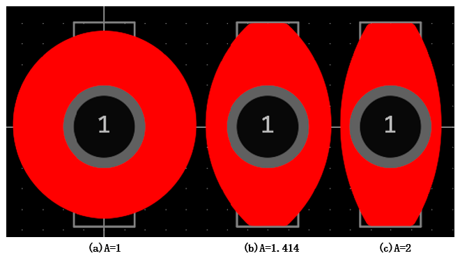
S is the length of the electrode side and A for the three different types of crescent-shaped electrodes is 1, 1.414, and 2, respectively. At A = 1, the circular arc is internally tangent to the square electrode, resulting in a close match between the droplet front and the electrode boundary. This configuration enables the effective three-phase contact line to attain its maximum length most rapidly and is therefore theoretically expected to provide optimal droplet actuation performance. At A = 1.414, the arc diameter is equal to the electrode diagonal, marking a geometric critical threshold at which the electrode profile transitions from a distinctly half-moon shape toward an approximately circular configuration. At A = 2, the arc diameter substantially exceeds the electrode length, progressively diminishing the half-moon features and causing the electrode geometry to approach a square shape.
As shown in Figure 3, the dashed circle is the droplet contact circle, and the EWOD tension generated at each point on the three-phase contact line when energization is performed is
Figure 3.
Schematic diagram of half-moon electrode with droplet profile.
γSG is the “solid–gas” surface tension, and γSL is the “solid–liquid” surface tension.
The total dielectric force acting on the effective three-phase contact line is directed toward the energized electrode. After integration
where C denotes the capacitance per unit area of the electric double layer, V represents the applied voltage, and L denotes the length of the three-phase contact line.
FEWOD = fer∙L
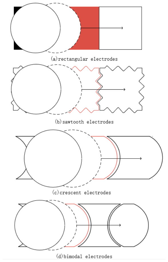
As indicated by Equation (5), FEWOD increases with the length of the three-phase contact line L. Compared with the rectangular and serrated driving electrodes, the crescent-shaped driving electrode provides a relatively uniform and longer three-phase contact line, thereby generating a greater electrowetting force on the droplet and facilitating its actuation. The droplet can be successfully actuated on the crescent-shaped electrode at a voltage lower than those required by the rectangular and serrated electrodes, indicating that the crescent-shaped design can effectively reduce the driving voltage of the digital microfluidic chip. As shown in Figure 4d, following the design principle of the crescent-shaped electrode, a double-crescent electrode was developed by symmetrically arranging identical crescent-shaped arcs on both sides of the electrode, thereby enhancing droplet actuation capability in both directions.
Calculations are made after points have been scored.
FEWOD is proportional to the three-phase contact line L from Equation (4). Therefore, the larger the three-phase contact line L, the larger its FEWOD. In comparison with the rectangular and serrated drive electrodes, the three-phase contact line of the droplet on the crescent drive electrode is relatively uniform and it is the largest, in which case its droplet force is the largest and it is easier to make the droplet drive. When driving the droplets at a lower voltage than the rectangular and sawtooth drives, the crescent drive voltage is also able to drive the droplets successfully, thus realizing the purpose of reducing the drive voltage of the digital microfluidic chip. The left and right sides of the double half-moon serrated electrodes adopt this principle by symmetrically placing crescent-shaped arcs with the same parameters, which improves the droplet driving ability in both directions.
3. DMF Chip Design and Fabrication
DMF Chip Design
Common electrode shapes are rectangular [32,33], serrated [34], and crescent [35], as shown in Figure 4. Figure 4a shows the rectangular electrode, which is the most basic and the first used electrode and possesses the advantages of symmetry and a simple shape, but it is easy to produce the edge electric field effect, which may lead to droplet behavior at the edge that is difficult to precisely control, as well as droplet deformation, lack of control, and so on. Figure 4b shows the sawtooth electrode, which can grow the three-phase contact line compared to the matrix electrode, which can lead to enhanced electrical wetting force, giving faster velocity of the droplets, which can be controlled using a lower voltage. At the same time, due to the overlap between the electrodes, droplet transportation can be made more continuous and smooth. However, the disadvantages of sawtooth electrodes are also obvious; the electric field distribution is very complex and susceptible to voltage breakdown. Figure 4c shows a crescent-shaped electrode, which can make the three-phase contact line longer due to the similarity of the arc of the crescent-shaped electrode to the contour of the droplet, thus providing a larger droplet driving force to drive the droplet at a faster and more uniform rate. In unidirectional movement, droplet velocity is significantly increased compared to rectangular and sawtooth electrodes. Figure 4d shows a double half-moon electrode, which needs to be used in combination with a similar elliptical electrode. The double meniscus electrode adds the other side of the meniscus symmetrically to the single meniscus electrode so that the droplet drive tends to be the same on both sides. Compared with the previous single half-moon electrode, the speed of bi-directional movement of droplets is enhanced, which compensates for the lack of unidirectional droplet driving ability. Although the double half-moon electrode improves the driving ability of the droplet in the left and right directions, if it is subjected to a compositional electrode arrangement, its top and bottom directions are still rectangular electrodes, and the driving ability of the droplet and the driving voltage are not improved.
Figure 4.
Common electrode shapes.
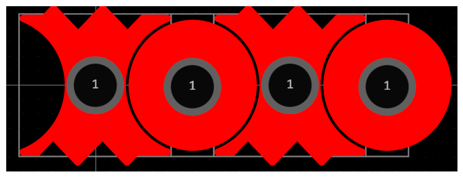
In this paper, the characteristics of the double half-moon electrode and the sawtooth electrode are combined to form a double half-moon sawtooth electrode, as shown in Figure 5. Double half-moon serrated electrodes are used in combination with ellipsoid-like electrodes in both the left and right directions to significantly enhance droplet mobility. And, in the upper and lower directions, the flat rectangular edges are designed as serrated edges, the liquid droplets can move continuously and rapidly, the electrodes can be arranged in convenient combinations with the ability to switch the direction of movement of liquid droplets freely in all directions, and they can be closely linked with the liquid separation tank, reaction tank, and waste liquid tank.
Figure 5.
Double half-moon serrated electrodes and combination electrodes.
Although the geometric ratio A varies among the different designs, all electrodes were constructed within the same 1 mm × 1 mm rectangular reference area. Consequently, the droplet footprint on each electrode is approximately 1 mm2, including the serrated and crescent-shaped electrodes used for comparison.
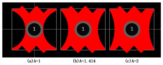
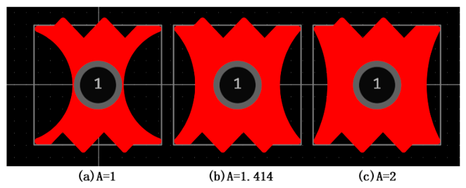
In this paper, we use PCB design software to design and fabricate the electrodes. The package design of electrodes according to different scale relations A is carried out in the software, as shown in Figure 6a, as an example of designing a double half-moon sawtooth electrode with A = 1. First, a circular pad with an inner diameter of 0.3 mm and an outer diameter of 0.4 mm is placed in the center of the canvas for linking. Next, using the document layer’s lines, place four lines of 0.01 mm line width and place the enclosure into a 1 mm*1 mm rectangle. Then, a top rectangular pad with a height of 0.7 mm and a width of 0.4 mm is placed in the middle of the pad. Place half-moon shaped top lines with a radius of 0.5 mm symmetrically on the left and right sides of the top rectangular pads. After placing the half-moon lines, the jagged lines on the top and bottom sides of the double half-moon sawtooth shape are drawn at the starting points of the two half-moon lines, but the two sides are not positively symmetrical; instead, they are drawn with reverse symmetry because they need to be arranged in combination. Finally, using the line tool, the gap is filled, and the double half-moon sawtooth electrodes with scale relations A = 1.414 and A = 2 are also designed and drawn according to this method, and the final double half-moon sawtooth electrodes with scale relations A = 1, 1.414, and 2 are shown in Figure 6.
Figure 6.
Double half-moon serrated electrodes.
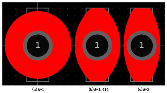
The ellipsoid-like electrodes used in conjunction with it are also exemplified by the proportionality relationship A = 1. As shown in Figure 7a, first, a circular pad with an inner diameter of 0.3 mm and an outer diameter of 0.4 mm is placed in the center of the canvas for linking. Next, using the document layer’s lines, place lines with a line width of 0.01 mm, but, unlike earlier, this needs to be placed separately. Lines of the same height as the double half-moon serrations are placed on the left and right sides, and lines 0.298 mm in length are placed on the top and bottom sides and they are combined together. Then, a top rectangular pad with a height of 0.82 mm and a width of 0.3 mm is placed in the middle of the pad. Based on the two double half-moon lines on either side of the double half-moon sawtooth shape, they were plotted keeping a distance of 20 μm. Finally, using the line tool, fill in the gaps. The ellipsoid-like combination electrodes of double half-moon serrated electrodes with scale relationships A = 1.414 and A = 2 were also designed and drawn according to this method. The ellipsoid-like combination electrodes with final scaling relationships A = 1, 1.414, 2 for the double half-moon serrated electrodes are shown in Figure 7.
Figure 7.
Ellipsoid-like combination electrodes.
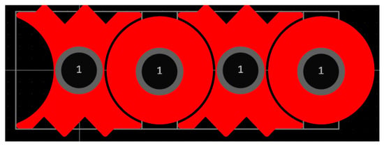
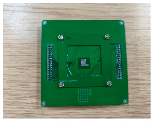
The electrodes are introduced into the circuit schematic to be arranged and combined, and the spacing between the electrodes is 20 μm, which will be fabricated into a circuit board, as shown in Figure 8. After a series of processes such as drilling, copper sinking, solder resisting, tin spraying, and AVI testing in the factory, the finished products are made. The surface of the electrode plate was covered with 5CST silicone oil as a lubricating link layer, and then a scratch-free, bubble-free, and hole-free cling film cut to the right size was placed on top as a dielectric layer. And, after that, 5CST silicone oil was spin-coated as a hydrophobic layer.
Figure 8.
Circuit board diagram.
4. DMF System Construction
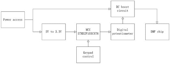
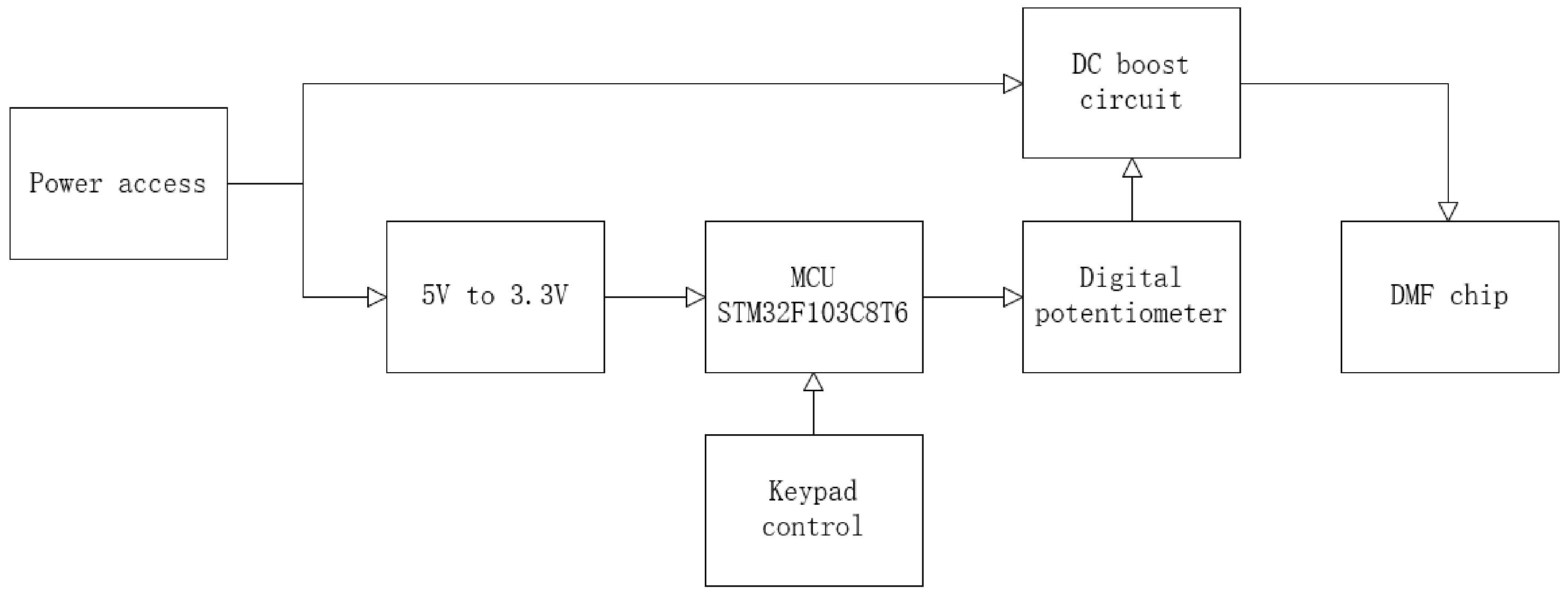
Figure 9 shows the DMF system design. The system mainly consists of three parts: the minimum system mainly controlled by the STM32F103C8T6 chip, the power supply circuit, and the DMF chip. Send up-down-right-right control commands to the control chip through the keypad, and the microcontroller processes and executes the relevant command operations and applies the droplet driving voltage signals to the corresponding electrodes of the DMF chip so as to realize the droplet motion control.
Figure 9.
DMF system flowchart.
4.1. Master Chip
The main control part consists of the master chip and its peripheral circuits. The master chip model is STM32F103C8T6, a 32-bit Cortex-M3 architecture microcontroller introduced by STMicroelectronics, which is highly praised by the majority of users for its powerful performance, rich peripherals, low price, high reliability, and other features. It has 37 general-purpose I/Os, 16 external interrupts, 4 timers, 2 hardware SPIs, 3 serial ports, and other peripherals, which meets the DMF system’s requirements for the peripheral aspects of the master chip. Its 20 KB SRAM and 128 KB Flash also meet the storage requirements of the master control chip.
4.2. Power Supply Circuit
In the DMF system constructed in this paper, the power supply circuit is divided into a 5 V to 3.3 V circuit and a DC boost circuit because the power supply voltage of the main control chip is 3.3 V and the voltage of the control electrode is over 100 V.
4.2.1. 5 V to 3.3 V Circuit
Because the power supply voltage of the master chip in the DMF system is 3.3 V, the digital circuit parts of the design are all powered by 3.3 V, the 5 V to 3.3 V circuit of the power supply chip use the U.S. AMS company introduced the 1117-3.3 chip. The regulator chip has high volume, low price, and other characteristics. Only 4 peripheral devices can be composed by a buck circuit, and the output current of the chip is 800 mA, which is much higher than the digital circuit part of the maximum power consumption current.
4.2.2. DC Boost Circuit
For the design of the boost circuit in this system, MAX1771 is selected as the core DC-DC boost controller chip, which is mainly used to effectively convert the lower input voltage into the voltage required to drive the digital microfluidic droplet. In the boost circuit, in order to make the output voltage adjustable, AD5272 is selected as a digital potentiometer.
The MAX1771 is a high-efficiency, wide-input-range DC-DC boost controller that integrates both pulse frequency modulation (PEN) and pulse width modulation (PWM) modes of operation. The MAX1771 contains an internal error amplifier, an oscillator, and a comparator, and these components work together to achieve a precise regulated voltage. It supports the external connection of N-channel MOSFETs as switching tubes, thus allowing the design to provide greater design flexibility by selecting the appropriate external power device based on specific power requirements.
The AD5272 chip is controlled by a resistor digital-to-analog converter (RDAC) register, which receives 10-bit or 8-bit data from the I2C serial interface and converts these digital values into the corresponding resistor tap positions to adjust the internal resistor array.
With these two chips, the power supply circuit is constructed, which not only realizes the power supply demand for the whole DMF system but also adjusts the output voltage to the electrodes by the program according to experimental demand.
4.3. DMF System Setup
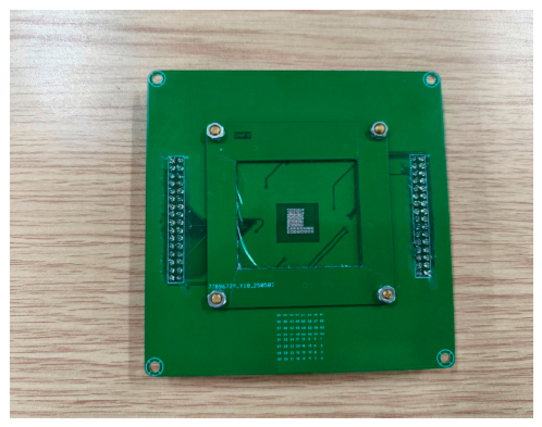
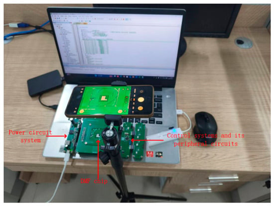
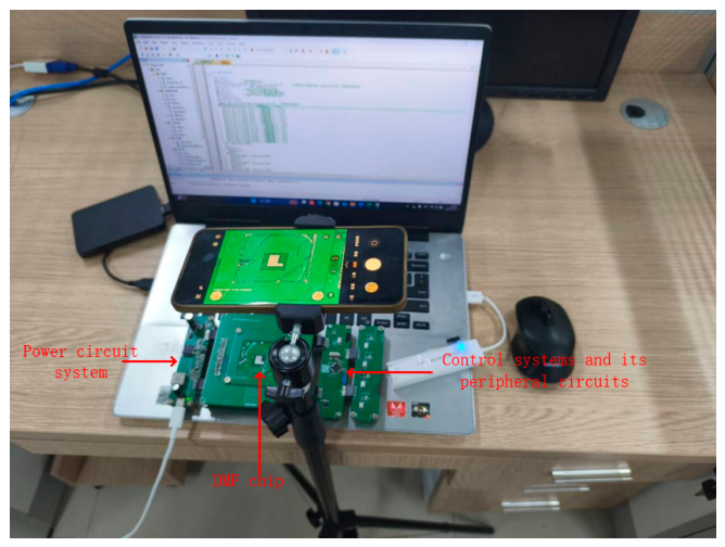
Figure 10 shows the constructed DMF system. The system is mainly composed of three parts: a control system, a DMF chip, and a power circuit system. The DMF chip is placed in the center, the power supply circuit system is placed on the left, the minimum control system with its peripheral circuits (key control) is placed on the right, and each part is linked through the row of pins and nuts. A signal is given to the microcontroller by manipulating the keys to realize the drive signal output and apply the drive voltage to the corresponding electrodes of the digital microfluidic chip. In addition, this system can observe the movement of the droplets in the chip through the cell phone camera and can also record and measure the process of controlling the droplets.
Figure 10.
DMF system.
5. Experimental Validation
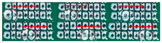
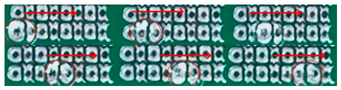
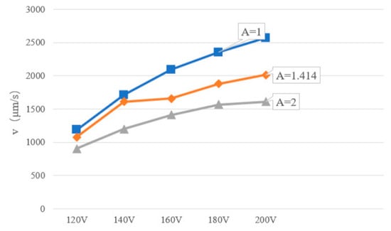
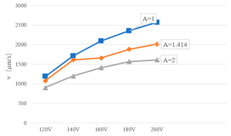
Before conducting the experiment, we set up the pre-work, set the voltage at which the experiment was to be conducted, and commissioned the equipment. A certain volume of aqueous droplets was then placed on the two adjacent driving electrodes of the DMF chip using a pipette and energized to perform the experiment. The voltage of the experiment was set up before the experiment was completed, and the movement of the droplets was recorded by a cell phone camera. The adjacent spacing of all three driving electrodes is 20 μm, and the voltage value is the RMS value of the voltage measured by the multimeter. Figure 11 shows a screenshot of the experimental video of the movement of a 1 μL droplet at a certain point in time, with the droplet moving from left to right. Figure 12 and Figure 13 are measured on three double half-moon serrated drive electrode structure chips at scaling relationships A = 1, 1.414, and 2, respectively, where the values of the scaling relationships are used to represent the different drive electrode shapes.
Figure 11.
Schematic diagram of droplet movement.
Figure 12.
Plot of average velocity of 1 μL droplet versus driving voltage.
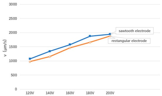
Figure 13.
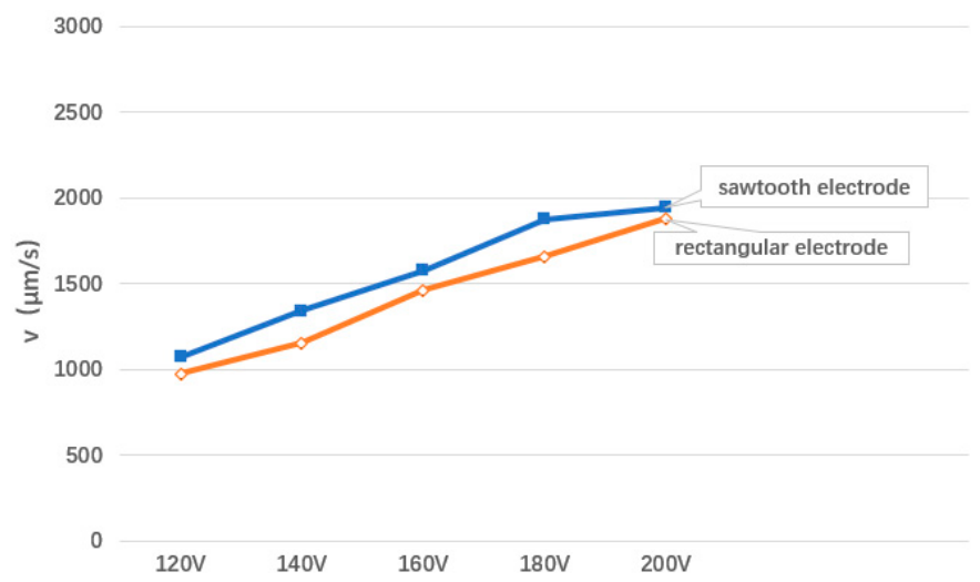
Plot of average sawtooth and rectangular velocity vs. drive voltage.
Figure 12 shows the relationship between the average velocity of 1 μL water droplets on three double half-moon sawtooth drive electrode chips and the driving voltage. The spacing between the electrodes and electrodes of the three drive electrodes is 20 μm, other experimental conditions are the same, and the voltage values are the RMS values of the voltages measured by the multimeter, in which the average velocities of the droplets were obtained from the analysis of the video of the droplet’s movement. To minimize experimental errors, droplet actuation tests were repeated ten times for each driving electrode at each applied voltage, and the average droplet velocity at each voltage was determined from the travel distance and corresponding travel time measured from each recorded video. The velocity of droplet motion on the driving electrode chips of all three structures grows as the driving voltage increases, but the average velocity of the droplets on the double half-moon sawtooth electrode chip with A = 1 is consistently the largest compared to the other two structures.
Experimental validation shows that when A = 1, the double half-moon shaped driving electrode chip drives the droplet best, and the effect of reducing the driving voltage is most obvious. Under the same experimental conditions, the driving voltage and the average velocity of the droplet when driving the droplet movement of this type of chip outperform the other two size-proportional driving electrode structures as an important measure of the performance of the digital microfluidic chip.
In order to facilitate the upper and lower combination of the electrodes and, at the same time, to make the droplets move continuously and rapidly, in the upper and lower directions, the flat rectangular edges are designed as serrated edges so that it has the ability to switch the direction of droplet movement freely in all directions and can be closely linked with the liquid separation tank, reaction tank, and waste liquid tank. Figure 13 shows a plot of the average speed of the sawtooth and rectangular edges versus the drive voltage. Because the same structure was used for the sawtooth edges of all three structures, one structure was randomly selected for the experiment. The experimental results show that the droplets on the sawtooth edge move faster than on the rectangular edge, regardless of the voltage.
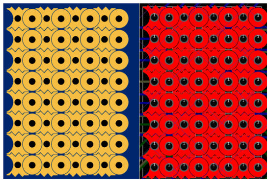
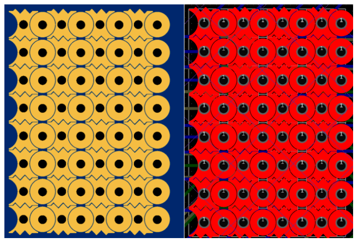
Figure 14 shows a combined arrangement of a double half-moon sawtooth electrode structure with a scale relationship A = 1 and its corresponding ellipsoid-like combination electrodes.
Figure 14.
Electrode combination arrangement.
6. Conclusions
In this paper, based on the relationship between the droplet force magnitude and the droplet effective three-phase contact line magnitude, relevant research has been carried out in the design and fabrication of a DMF chip and the construction of a DMF system, and three kinds of double half-moon serrated electrodes with three kinds of structures have been designed. Furthermore, droplet driving experiments have been carried out on the DMF chip, and the droplet driving capability of the three kinds of designed double half-moon serrated electrodes has been investigated through the experiments. The data obtained from the study show that the double half-moon sawtooth electrode with the proportionality relationship A = 1 drives the droplets best, and the droplets move with the largest average velocity. This double half-moon serrated electrode is able to maintain greater overlap with the droplet at the left and right edges, which can provide a larger initial driving force, while the serrated structure at the top and bottom edges has the advantage of aligning the electrode array. After testing, the DMF system built in this paper has the characteristics of high stability and convenient combination, and it is easy to build and easy to manipulate, which provides equipment support to reduce the manipulation voltage of a digital microfluidic chip.
Author Contributions
X.H.: conceptualization, methodology, formal analysis; X.Z.: writing—original draft, data curation, software, validation; B.X.: data curation, software, validation; H.C.: supervision, funding acquisition; C.H.: supervision, funding acquisition; C.X.: supervision, funding acquisition, writing—review and editing. All authors have read and agreed to the published version of the manuscript.
Funding
This study was funded by the Guangxi Natural Science Foundation of China (No. 2026GXNSFAA00641112).
Institutional Review Board Statement
Not applicable.
Informed Consent Statement
Not applicable.
Data Availability Statement
The datasets generated and/or analyzed during the current study are available from the corresponding author upon reasonable request.
Conflicts of Interest
The authors declare no conflicts of interest.
References
- Fair, R.B. Digital microfluidics: Is a true lab-on-a-chip possible? Microfluid. Nanofluid. 2007, 3, 245–281. [Google Scholar] [CrossRef] [Scilit]
- Wang, X.; Piao, Y.; Su, Y.; Wang, W. Driving and sorting of the fluorescent droplets on digital microfluidic platform. Microfluid. Nanofluid. 2018, 22, 129. [Google Scholar] [CrossRef] [Scilit]
- Xie, M.; Chen, T.; Xin, X.; Cai, Z.; Dong, C.; Lei, B. Multiplex detection of foodborne pathogens by real-time loop-mediated isothermal amplification on a digital microfluidic chip. Food Control 2022, 136, 108824. [Google Scholar] [CrossRef] [Scilit]
- Liu, X.; Ma, D.; Ye, H.; Hou, Y.; Bai, X.; Xing, Y.; Cheng, X.; Lin, B.; Lu, Y. Electrowetting-based digital microfluidics: Toward a full-functional miniaturized platform for biochemical and biological applications. TrAC Trends Anal. Chem. 2023, 166, 117153. [Google Scholar] [CrossRef] [Scilit]
- Abdelgawad, M. Digital microfluidics: Automating microscale liquid handling. IEEE Nanotechnol. Mag. 2020, 14, 6–23. [Google Scholar] [CrossRef] [Scilit]
- Li, K.; Lu, X.; Liao, J.; Chen, H.; Lin, W.; Zhao, Y.; Tang, D.; Li, C.; Tian, Z.; Zhu, Z.; et al. DNA-DISK: Automated end-to-end data storage via enzymatic single-nucleotide DNA synthesis and sequencing on digital microfluidics. Proc. Natl. Acad. Sci. USA 2024, 121, e2410164121. [Google Scholar] [CrossRef] [Scilit] [PubMed]
- Prathaban, S.N.; Zambry, N.S.; Ibrahim, F.; Ahmad, M.Y.; Jamaluddin, N.F.; Tee, T.S. Future electrodes for sepsis detection: Digital microfluidic biosensors from plant waste. Microfluid. Nanofluid. 2024, 28, 76. [Google Scholar] [CrossRef] [Scilit]
- Bai, H.; Hu, J.; Liu, T.; Wan, L.; Dong, C.; Luo, D.; Li, F.; Yuan, Z.; Tang, Y.; Chen, T.; et al. A sample-to-answer digital microfluidic multiplexed PCR system for syndromic pathogen detection in respiratory tract infection. Lab Chip 2025, 25, 1552–1564. [Google Scholar] [CrossRef] [Scilit] [PubMed]
- Zhai, J.; Liu, Y.; Ji, W.; Huang, X.; Wang, P.; Li, Y.; Li, H.; Wong, A.H.-H.; Zhou, X.; Chen, P.; et al. Drug screening on digital microfluidics for cancer precision medicine. Nat. Commun. 2024, 15, 4363. [Google Scholar] [CrossRef] [Scilit] [PubMed]
- Zhai, J.; Li, C.; Li, H.; Yi, S.; Yang, N.; Miao, K.; Deng, C.; Jia, Y.; Mak, P.I.; Martins, R.P. Cancer drug screening with an on-chip multi-drug dispenser in digital microfluidics. Lab Chip 2021, 21, 4749–4759. [Google Scholar] [CrossRef] [Scilit] [PubMed]
- Shi, J.; Fu, P.; Zheng, W. Lifetime improvement of digital microfluidic biochips based on the IWOA. Microelectron. Reliab. 2021, 123, 114182. [Google Scholar] [CrossRef] [Scilit]
- Kasputis, T.; Yeh, P.-C.; Liu, L.; Marano, J.; Weger-Lucarelli, J.; Du, K.; Lin, L.; Chen, J. Development of a self-powered digital LAMP microfluidic chip (SP-dChip) for the detection of emerging viruses. Lab Chip 2024, 24, 3490–3497. [Google Scholar] [CrossRef] [Scilit] [PubMed]
- Washburn, J.; Millington, D.S. Digital microfluidics in newborn screening for mucopolysaccharidoses: A progress report. Int. J. Neonatal Screen. 2020, 6, 78. [Google Scholar] [CrossRef] [Scilit] [PubMed]
- Shen, R.; Lv, A.M.; Yi, S.; Wang, P.; Mak, P.-I.; Martins, R.P.; Jia, Y. Nucleic acid analysis on electrowetting-based digital microfluidics. TrAC Trends Anal. Chem. 2023, 158, 116826, Corrigendum in TrAC Trends Anal. Chem. 2024, 171, 117535. [Google Scholar] [CrossRef] [Scilit]
- Xu, X.; Cai, L.; Liang, S.; Zhang, Q.; Lin, S.; Li, M.; Yang, Q.; Li, C.; Han, Z.; Yang, C. Digital microfluidics for biological analysis and applications. Lab Chip 2023, 23, 1169–1191. [Google Scholar] [CrossRef] [Scilit] [PubMed]
- Kim, T.; Kim, J.; Kang, J.W.; Kwon, S.B.; Hong, J. Compact three-dimensional digital microfluidic platforms with programmable contact charge electrophoresis actuation. Langmuir 2022, 38, 5759–5764. [Google Scholar] [CrossRef] [Scilit] [PubMed]
- Bae, S.J.; Lee, S.J.; Im, D.J. Simultaneous separating, splitting, collecting, and dispensing by droplet pinch-off for droplet cell culture. Small 2024, 20, e2309062. [Google Scholar] [CrossRef] [Scilit] [PubMed]
- Ye, W.-Q.; Wei, Y.-Y.; Wang, D.-N.; Yang, C.G.; Xu, Z.R. A digital microfluidic platform based on a near-infrared light-responsive shape-memory micropillar array. Lab Chip 2021, 21, 1131–1138. [Google Scholar] [CrossRef] [Scilit] [PubMed]
- Song, Y.; Hu, Y.; Zhang, Y.; Li, G.; Wang, D.; Yang, Y.; Zhang, Y.; Zhang, Y.; Zhu, W.; Li, J.; et al. Flexible tri-switchable wettability surface for versatile droplet manipulations. ACS Appl. Mater. Interfaces 2022, 14, 37248–37256. [Google Scholar] [CrossRef] [Scilit] [PubMed]
- Zhang, P.; Chen, C.; Su, X.; Mai, J.; Gu, Y.; Tian, Z.; Zhu, H.; Zhong, Z.; Fu, H.; Yang, S.; et al. Acoustic streaming vortices enable contactless, digital control of droplets. Sci. Adv. 2020, 6, eaba0606. [Google Scholar] [CrossRef] [Scilit] [PubMed]
- Huang, J.; Ren, X.; Zhou, Q.; Zhou, J.; Xu, Z. Flexible acoustic lens-based surface acoustic wave device for manipulation and directional transport of micro-particles. Ultrasonics 2023, 128, 106865. [Google Scholar] [CrossRef] [Scilit] [PubMed]
- Strassner, J.; Doering, C.; Oliveira, E.; Fouckhardt, H. Optoelectrowetting (OEW) with push-actuation of microdroplets at small frequencies and OEW equations revisited. Sens. Actuators A Phys. 2022, 334, 113331. [Google Scholar] [CrossRef] [Scilit]
- Doering, C.; Strassner, J.; Fouckhardt, H. Microdroplet actuation via light line optoelectrowetting (LL-OEW). Int. J. Anal. Chem. 2021, 2021, 3402411. [Google Scholar] [CrossRef] [Scilit] [PubMed]
- Li, Y.-J.; Echtermeyer, D.; Cahill, B.P.; Pliquett, U. Non-linearity and dynamics of low-voltage electrowetting and dewetting. Phys. Chem. Chem. Phys. 2019, 21, 18290–18299. [Google Scholar] [CrossRef] [Scilit] [PubMed]
- Datta, S.; Kumar, P.; Das, A.K. Manipulation of droplets by electrostatic actuation and the related hydrodynamics (review). J. Indian Inst. Sci. 2019, 99, 121–141. [Google Scholar] [CrossRef] [Scilit]
- Khanna, M.; Roy, S.; Mathur, A.; Dubey, A.K.; Vashisth, R. Analysis of voltage distribution in electrowetting on dielectric (EWOD) system. Mater. Today Proc. 2021, 38, 179–185. [Google Scholar] [CrossRef] [Scilit]
- Türk, S.; Schug, A.; Viga, R.; Jupe, A.; Vogt, H. Optimization of the dielectric layer for electrowetting on dielectric. Integration 2019, 67, 50–59. [Google Scholar] [CrossRef] [Scilit]
- Sohail, S.; Jaffery, Z.; Biswas, K. Study of threshold voltage for different electrode shapes in electrowetting device. Mater. Res. Express 2019, 6, 046414. [Google Scholar] [CrossRef] [Scilit]
- Sohail, S.; Jaffery, Z.A.; Biswas, K. Jigsaw electrode design for electrowetting devices. Micro Nano Lett. 2019, 14, 1046–1051. [Google Scholar] [CrossRef] [Scilit]
- Wang, W.; Rui, X.; Sheng, W.; Wang, Q.; Wang, Q.; Zhang, K.; Riaud, A.; Zhou, J. An asymmetric electrode for directional droplet motion on digital microfluidic platforms. Sens. Actuators B Chem. 2020, 324, 128763. [Google Scholar] [CrossRef] [Scilit]
- Guo, J.; Lin, L.; Zhao, K.; Song, Y.; Huang, M.; Zhu, Z.; Zhou, L.; Yang, C. Auto-Affitech: An automated ligand binding affinity evaluation platform using digital microfluidics with a bidirectional magnetic separation method. Lab Chip 2020, 20, 1577–1585. [Google Scholar] [CrossRef] [Scilit] [PubMed]
- Kremers, T.; Thelen, S.; Bosbach, N.; Schnakenberg, U. PortaDrop: A portable digital microfluidic platform providing versatile opportunities for lab-on-a-chip applications. PLoS ONE 2020, 15, e0238581. [Google Scholar] [CrossRef] [Scilit] [PubMed]
- Wang, Z.; Chen, L.; Bian, X. Design of crescent splitting electrodes in EWOD device. J. Appl. Fluid Mech. 2020, 13, 1437–1442. [Google Scholar] [CrossRef] [Scilit]
- Torabinia, M.; Dakarapu, U.S.; Asgari, P.; Jeon, J.; Moon, H. Electrowetting-on-dielectric (EWOD) digital microfluidic device for in-line workup in organic reactions: A critical step in the drug discovery work cycle. Sens. Actuators B Chem. 2021, 330, 129252. [Google Scholar] [CrossRef] [Scilit]
- von der Ecken, S.; Sklavounos, A.A.; Wheeler, A.R. Vertical addressing of 1-plane electrodes for digital microfluidics. Adv. Mater. Technol. 2022, 7, 2101251. [Google Scholar] [CrossRef] [Scilit]
- Verheijen, H.J.J.; Prins, M.W.J. Reversible Electrowetting and Trapping of Charge: Model and Experiments. Langmuir 1999, 15, 6616–6620. [Google Scholar] [CrossRef] [Scilit]
Disclaimer/Publisher’s Note: The statements, opinions and data contained in all publications are solely those of the individual author(s) and contributor(s) and not of MDPI and/or the editor(s). MDPI and/or the editor(s) disclaim responsibility for any injury to people or property resulting from any ideas, methods, instructions or products referred to in the content. |
© 2026 by the authors. Licensee MDPI, Basel, Switzerland. This article is an open access article distributed under the terms and conditions of the Creative Commons Attribution (CC BY) license.