


Abstract
To address the challenge of achieving a balanced match between internal thermal resistance bottlenecks and enhanced external heat dissipation in high-power-density liquid-cooled IGBT modules, this paper establishes a three-dimensional conjugate heat transfer model comprising the IGBT/FRD chip, the packaging layer, the substrate, the elliptical pin-fin heat sink, and the fluid domain, and identifies the thermal resistance bottlenecks along the main heat transfer paths through interlayer temperature-drop decomposition. Furthermore, the thermal shortcut number (SN), defined based on the ratio of overall equivalent thermal resistances, is introduced as a supplementary metric to evaluate the relative changes in overall thermal resistance among different heat dissipation structures. In conjunction with the maximum chip temperature and pressure drop, the effects of cooling conditions, pin-fin structural parameters, and zonal regulation strategies on the thermal performance and flow resistance of the module are investigated. The results indicate that when the coolant flow rate is increased from 4 L/min to 12 L/min, the maximum chip temperature decreases by 16.27 K. However, the pressure drop increases from 1.93 kPa to 13.59 kPa, demonstrating a clear diminishing marginal return. While global thinning of the pin fins, reduction in their cross-sectional dimensions and lowering of their height can reduce the pressure drop, these measures weaken the solid–liquid heat transfer area and the capacity of external thermal shortcut; by contrast, zone-based control and flow-direction gradient structures can effectively improve the thermal–flow matching; amongst these, the local high-temperature suppression structure reduces the maximum chip temperature by 0.84 K, lowers the pressure drop by 3.89%, and increases the SN to 1.003; while the height-gradient structure along the flow direction reduces the pressure drop by 17.91% with a temperature rise of only 0.63 K. The study indicates that the optimisation of thermal management for liquid-cooled IGBT modules should balance the reduction of internal thermal resistance with the enhancement of external heat dissipation, in order to establish an external thermal shortcut characterized by low thermal resistance and low pressure drop that are well-matched to the distribution of heat sources, thereby achieving the synergistic optimisation of thermal and flow performance.
1. Introduction
As electric drive systems for new energy vehicles evolve toward higher power density and greater integration, the thermal management challenge for IGBT modules in traction inverters is becoming increasingly prominent. The losses generated by IGBT and FRD chips under high-current, high-frequency switching conditions are predominantly converted into heat; if this heat cannot be promptly transferred to the coolant via the package structure, substrate, and liquid-cooled heat sink, it will lead to an increase in chip junction temperature, intensification of local hotspots, and a decline in thermal reliability. Liquid-cooled heat dissipation structures can significantly shorten the heat transfer path between the chips and the coolant, making them an important approach to thermal management for automotive power modules [1]. Among these, pin-fin heat sinks have been widely investigated for cooling power modules with high heat flux density due to their large solid–liquid heat transfer area and strong flow-disturbing effects [2,3].
In liquid-cooled IGBT modules, heat generated by the chips is transferred through the internal encapsulation layer to the substrate and then undergoes heat exchange with the coolant via the external pin-fin heat sink before being ultimately dissipated. Consequently, the external heat dissipation structure and flow conditions not only determine the strength of the cooling boundary condition but also directly affect the efficiency of heat transfer from the solid structure to the coolant. When the coolant flow rate is insufficient, the local heat transfer coefficient is low, or the pin-fin structure is poorly matched to the flow path, the external heat dissipation side may become a thermal bottleneck that limits heat transfer; conversely, through rational design of the pin-fin geometry, coolant flow conditions, and zoned-control strategies, the external thermal resistance can be reduced and a more efficient heat transfer path established—thereby enabling a thermal shortcut effect.
Researchers have conducted extensive studies on enhancing the external heat dissipation of IGBT modules, with a focus on optimizing liquid-cooling structures and operating parameters. Hitachi et al. proposed a direct liquid-cooled IGBT module for automotive applications and optimized the cooling fin geometry through thermal-fluid simulation, effectively reducing the thermal resistance of the module [4]. Lee was among the first to employ CFD methods to optimize the design of the pin-fin array in integrated liquid-cooled IGBT modules, noting that both chip-to-chip temperature uniformity and the maximum junction temperature are critical metrics for evaluating thermal performance [5]. Wu et al. investigated the effects of pin-fin spacing, coolant flow rate, and temperature on the junction temperature and temperature uniformity of IGBT modules, finding that a dual-channel non-uniform pin-fin configuration could significantly improve module cooling performance; however, their study focused primarily on optimizing the external heat dissipation structure, with limited consideration of synergistic matching between the module’s internal thermal resistance and its enhanced external heat dissipation [6]. To address thermal management challenges including heat dissipation capability and temperature uniformity in high-power-density IGBT modules, Li et al. proposed a three-objective topology optimization method for liquid-cooled heat sinks, using average temperature, temperature variance, and flow losses as optimization objectives. This approach reduced the average temperature and temperature variance by 10.43% and 44.37%, respectively; however, because the study primarily employed a two-dimensional model for topology optimization, it struggled to fully reflect the influence of the actual internal thermal resistance and complete heat transfer pathways within the module [7]. In recent years, numerous researchers have further investigated the thermo-hydraulic performance evaluation and structural optimization of pin-fin heat sinks. For example, Saghir et al. investigated the thermal and flow performance of wavy and straight pin-fin configurations, demonstrating that pin-fin geometry influences both heat transfer and flow characteristics [8]. Kumar et al. numerically investigated the effects of streamwise variations in pin-fin height on the flow and heat transfer characteristics of microchannel heat sinks, finding that different height distributions yield distinct thermo-hydraulic performance outcomes [9]. Gao et al. [10] combined experimental and numerical approaches to compare the temperature distribution, pressure drop, and overall thermo-hydraulic performance of micro-pin-fin heat sinks featuring five different streamwise height profiles. Their results showed that the overall performance of these height distributions varies with inlet flow rate. Zhang et al. [11] focused on liquid-cooled cold plates for high-power motor controllers with discrete heat sources and employed a multi-parameter, zonal collaborative optimization strategy to improve maximum temperature, temperature uniformity, and pressure drop—thereby enhancing thermal management efficiency.
In summary, existing thermal design studies of liquid-cooled IGBT modules have primarily focused on indicators such as maximum junction temperature, average temperature, and total thermal resistance, which reflect the overall cooling capacity of the heat dissipation structure; however, research into the relationship between heat transfer pathways and flow resistance during the process of enhancing external heat dissipation remains insufficient. It is worth noting that thermal management research for high-density integrated electronic packaging has increasingly focused on controlling heat transfer pathways and local hotspots. Benelhaouare et al. [12] investigated thermal management strategies such as TSVs, microchannel coolers, and micro-pin fin heat sinks in 3D-SiP architectures, emphasizing the reduction of internal package hotspots by optimizing heat transfer paths and enhancing localized cooling capacity. This study demonstrates that, for high-density integrated electronic systems, internal heat transfer pathways and thermal resistance distribution are critical factors affecting overall thermal performance. Although 3D-SiP and liquid-cooled IGBT modules differ in device architecture and cooling methods, their focus on heat transfer pathways, local hotspots, and thermal resistance control provides a valuable supplementary background for the research presented in this paper. For pin-fin liquid cooling structures, increasing the coolant flow rate, the number of pin fins, the cross-sectional dimensions, and the height of the pin fins can generally enhance heat transfer but simultaneously increase flow resistance and pumping power. Conversely, reducing pin-fin density, cross-sectional dimensions, or pin-fin height can lower pressure drop, but these measures may weaken local heat transfer capacity, leading to insufficient cooling in localized regions or even exacerbating temperature non-uniformity [13,14,15]. Therefore, the optimization of the external heat dissipation structure for liquid-cooled IGBT modules should not simply aim for the lowest junction temperature or the lowest pressure drop; rather, it should comprehensively consider the benefits of cooling, the loss of flow resistance, and the ability to suppress local hotspots, thereby achieving synergistic optimization between enhanced heat transfer and flow performance.
On this basis, this paper carries out analysis from the perspectives of cooling conditions, fin structure parameters, structure-flow coupling, and external heat dissipation mechanisms, based on a complete liquid-cooled IGBT module. It investigates the influence of inlet temperature, coolant flow rate, pin-fin sparsification, cross-sectional dimensions, height variation, and zoned-control structures on the maximum chip temperature, pressure drop, heat flux paths, and the distribution of external thermal resistance; furthermore, it examines the matching relationship between the internal packaging thermal resistance of liquid-cooled IGBT modules and their external liquid cooling heat dissipation capability, analyzing heat transfer characteristics via interlayer temperature-drop decomposition and regulation of the external heat dissipation structure. The results provide a basis for subsequent synergistic optimization based on thermal bottleneck reduction and thermal shortcut enhancement.
2. Numerical Models and Evaluation Methods
2.1. Structure and Modelling Simplification of Liquid-Cooled IGBT Modules
The liquid-cooled IGBT module adopts a three-phase bridge configuration, with each phase comprising two bridge arms. Each bridge arm contains three IGBT chips and three FRD chips connected in parallel. The entire module contains 18 IGBT chips and 18 FRD chips. A schematic diagram of the module structure is shown in Figure 1. The liquid-cooling section consists of the baseplate, elliptical pin-fin heat sinks, the external housing, and the fluid domain. An integrated baseplate-pin-fin structure is adopted in this study. The coolant enters the flow channel through the inlet, passes through the pin-fin array region, undergoes convective heat transfer with the pin-fin surfaces and the baseplate’s bottom surface, and finally exits through the outlet.
Figure 1.
Schematic diagram of the IGBT module structure: (a) cross-sectional view of the IGBT module and elliptical pin-fin liquid-cooled heat sink; (b) three-dimensional view of the IGBT module.
To strike a balance between computational accuracy and efficiency, the model retains the primary heat transfer structures, including the IGBT/FRD chips, solder layers, direct-bonded copper (DBC) ceramic layer, copper layers, substrate, heat sink, and fluid domain. Details that have a minimal impact on the overall heat transfer path, such as bonding wires, bolts, chamfers, and mounting holes, are neglected. The coolant enters the pin-fin region through the inlet, where it undergoes convective heat transfer with the pin-fin walls and the underside of the substrate, and subsequently exits through the outlet.
2.2. Heat Source Loading and Boundary Conditions
The heat generated during the operation of the IGBT module primarily originates from power losses in the IGBT and FRD chips. In this paper, the steady-state average power losses are used as the heat source input; the device losses obtained under typical motor controller operating conditions are treated as equivalent volumetric heat sources and applied to the corresponding chip areas. The power dissipation of a single IGBT chip is 165.07 W, while that of a single FRD chip is 35.33 W; based on the geometric dimensions of the chips, the volumetric heat sources for the IGBT and FRD are 2.08 × 10¹⁰ W/m3 and 8.56 × 10⁹ W/m3, respectively. Under actual electric vehicle operating conditions, the power losses of traction inverter modules vary with driving conditions and motor torque demands. Taking the CLTC-P driving cycle as an example, vehicle operation can be divided into typical intervals, such as low-speed congested driving, medium-speed free-flow driving, and high-speed cruising, each characterized by distinct power-loss profiles. When designing heat dissipation structures for specific operating conditions, the power losses at representative operating points or the average power losses over typical intervals can be selected and modeled as equivalent steady-state heat sources to analyze the temperature distribution and flow resistance of different heat dissipation configurations. Accordingly, this study adopts fixed chip-level heat sources to ensure a consistent basis for comparing the thermal and flow performance of different structural parameters under the reference operating condition. The chip-level heat source inputs are kept consistent in subsequent calculations unless otherwise specified.
The material parameters are set according to the typical operating temperatures of each module. The main material parameters are shown in Table 1. A 50% ethylene glycol-water solution is used as the coolant. The inlet temperature is 65 °C, and the inlet flow rate is 8 L/min; the outlet is configured as a pressure outlet. Thermal coupling contact is employed between the solid packaging layers, while conjugate heat transfer boundary conditions are applied at the solid–liquid interface. The non-primary outer surfaces are treated as adiabatic boundaries to highlight the primary heat transfer path, whereby heat from the chip is transferred through the packaging layers, substrate, and heat sink structure to the coolant.
Table 1.
Main material physical properties of the IGBT module.
From an engineering application perspective, the coolant temperature and flow rate of automotive traction inverters vary with cooling system design, vehicle operating conditions, and thermal management strategies. For example, publicly available specifications for selected automotive high-voltage inverter products from Eaton indicate liquid-cooling flow rates on the order of 6–8 L/min and coolant temperature limits of approximately 65–70 °C. These specifications suggest that the inlet temperature of 65 °C and the reference flow rate of 8 L/min adopted in this study have practical engineering relevance [16]. However, design parameters vary among vehicles, inverters, and cooling circuits. Therefore, the reference operating conditions considered herein should be regarded as representative conditions for comparative structural performance evaluation rather than as universally applicable operating conditions for all electric vehicle traction inverters.
In addition, the chip-level losses are treated as fixed volumetric heat sources in this study, primarily to investigate the effects of cooling boundary conditions and heat dissipation configuration parameters on module thermal performance under a given thermal load. In actual traction inverters, power losses depend on vehicle load, motor operating conditions, and the electrical operating conditions of power semiconductor devices. Consequently, the heat source configuration adopted in this study does not capture instantaneous loss variations over a complete driving cycle. The results therefore primarily characterize the steady-state thermal and flow behavior under the specified thermal load and cooling conditions, rather than the transient junction-temperature response throughout an entire vehicle driving cycle.
2.3. Control Equations, Grid Independence and Model Validation
The heat transfer process in the liquid-cooled IGBT module involves thermal conduction through the solid packaging layers, thermal diffusion within the substrate and pin fins, and convective heat transfer in the coolant. The solid regions are governed by the steady-state heat conduction equation; volume heat sources are applied to the IGBT and FRD chip regions, while no internal heat sources are assigned to non-active heat-generating regions such as the solder layers, DBC layers, substrate, and pin fins. The fluid region is solved using the continuity, momentum, and energy equations for an incompressible fluid. The solid–liquid interface satisfies the conditions of temperature continuity and heat flux continuity, enabling coupled heat transfer calculations among the packaging structure, the pin-fin walls, and the coolant. The specific governing equations can be found in Reference [17].
To ensure computational accuracy, local mesh refinement is carried out in regions with significant temperature or velocity gradients (such as the chips, solder layers, DBC ceramic layer, and pin-fin surfaces), while a grid-independence verification is also conducted. When the number of mesh elements increases from 5.2 million to 8.9 million, the maximum junction temperature decreases from 413.67 K to 413.27 K, corresponding to a difference of 0.4 K; and the pressure drop decreases from 6.81 kPa to 6.50 kPa, representing a variation of 4.76%. When the mesh elements are further increased to 12.3 million, the maximum junction temperature reaches 413.13 K, showing a mere difference of 0.14 K compared to the 8.9-million-grid case; the pressure drop is 6.65 kPa, corresponding to a variation of 2.31% compared with that at 8.90 million elements. These results indicate that both the maximum junction temperature and pressure drop gradually converge with increasing mesh density, demonstrating that additional mesh refinement exerts negligible influence on the computational results. Consequently, this paper selects 8.9 million mesh elements as the base mesh for the subsequent internal thermal bottleneck analysis, as shown in Table 2.
Table 2.
Mesh independence verification results.
To validate the accuracy of the numerical model, experimental data for an SGM820PB8B3TFM liquid-cooled IGBT module reported in Reference [18] are selected for comparison. The numerical model presented in this paper is established based on the chip layout, major packaging structures, and liquid-cooled heat dissipation configuration of this module. The validation conditions employ the same peak power loss of the motor controller and cooling boundary conditions as those in the literature experiments, with a coolant inlet temperature of 65 °C and a flow rate of 8 L/min. The literature experiment measured a maximum junction temperature of 136.9 °C for the IGBT chip, while the numerical model in this paper calculated a maximum junction temperature of 413.27 K (140.12 °C); the difference between the two is 3.22 °C, representing a relative error of 2.35%. The deviation may be attributed to the appropriate simplification of non-primary heat-transfer structures, such as bonding wires, bolts, and local chamfers. Consequently, a certain deviation still exists between the experimental and calculated results. In the literature, the simulated junction temperature of the IGBT under the same operating conditions is 139.7 °C, which is closer to the result in this paper, with a difference of approximately 0.42 °C between the two. This indicates good agreement between the simulation results of the present study and those reported in previous research. It should be noted that model validation in this study is primarily based on the experimental data reported in Ref. [18]. The validation applies to the baseline structure under the corresponding cooling conditions and does not involve direct experimental validation of the proposed zonal regulation and streamwise-gradient pin-fin structures. Therefore, the results presented herein should be regarded as a numerical comparison and structural optimization analysis conducted on the basis of baseline-condition validation.
Furthermore, the 3.22 °C deviation between the present model predictions and the experimental results reported in the literature reflects the discrepancy between numerical predictions and experimental measurements under the baseline operating conditions. This deviation does not directly represent the overall predictive uncertainty of the model, nor does it invalidate the effectiveness of structural optimizations that produce relatively small temperature reductions. Overall, the existing validation results primarily demonstrate the predictive capability of the baseline model and provide a basis for subsequent numerical comparisons among different heat dissipation structures. However, in the absence of direct experimental validation of the optimized structures, the actual magnitude of the temperature reduction and its significance relative to the overall predictive uncertainty of the model remain to be further verified.
The comparison results indicate that the model developed in this paper is capable of accurately predicting the maximum junction temperature of this IGBT module under peak operating conditions. Taking into account the mesh-independence tests, the conservation of input and output energy, and comparisons with experimental data from modules modeled using the same approach, it can be concluded that the three-dimensional coupled heat transfer model established in this paper possesses good computational accuracy and can be utilized for subsequent analyses of external liquid cooling and co-optimization.
2.4. Inter-Layer Temperature Drop and Methods for Assessing Thermal Bottlenecks
In order to quantitatively determine the thermal resistance contributions of each packaging layer within a liquid-cooled IGBT module, this paper selects the IGBT chip with the highest temperature as the target chip and extracts the average temperatures on the upper and lower surfaces of the key structural layers along its primary heat transfer paths. The key heat transfer paths include the chip, the solder layer beneath the chip, the copper layer on the DBC, the ceramic layer of the DBC, the copper layer beneath the DBC, the solder layer beneath the DBC, and the baseplate—among other areas. The schematic diagram is shown in Figure 2.
Figure 2.
Schematic diagram of the target chip and key heat transfer path.
The inlet temperature and flow rate of the coolant not only affect the overall temperature of the module but also alter the external heat transfer intensity, the temperature rise of the coolant, and the flow resistance. In particular, the inlet temperature primarily determines the temperature reference of the cooling boundary, causing the overall temperature field of the module to shift upward or downward. In contrast, the coolant flow rate influences the degree of mitigation of the external thermal bottlenecks and the formation of heat shortcuts by altering the velocity field within the flow channels, the heat capacity flux rate, and the convective heat transfer capacity at the pin-fin surfaces. To clarify the patterns governing the influence of the cooling boundary on the module’s external heat dissipation performance, this paper varies the coolant inlet temperature and flow rate while maintaining the baseline pin-fin structure and chip heat sources unchanged. Using the baseline condition as a reference, the study analyzes the variation patterns of the maximum chip temperature, outlet temperature, and inlet–outlet pressure drop [19]. In the baseline case, the coolant inlet temperature is 65 °C, and the flow rate is 8 L/min; the volumetric heat sources of the IGBT and FRD are 2.08 × 10¹⁰ W/m3 and 8.56 × 10⁹ W/m3, respectively, and the inlet–outlet pressure drop is 6.50 kPa.
To quantitatively compare the effects of different cooling conditions and pin-fin structures on the overall heat dissipation performance of the liquid-cooled IGBT module, this study introduces the thermal shortcut number (SN) to characterize the change in overall equivalent thermal resistance relative to the baseline condition. The thermal bottlenecks and thermal shortcut analysis methods proposed in Refs. [20,21] primarily rely on the vector relationship between local heat flux density and temperature gradients to identify local bottleneck regions and potential shortcuts in heat transfer. These methods provide a basis for heat sink optimization through the spatial distributions of relevant characteristic quantities. In contrast to these methods, which focus on local heat transfer characteristics, the present study investigates the thermal performance matching between the multilayer internal packaging structure and the external liquid-cooling structure of the IGBT module. To quantitatively compare the relative heat dissipation performance under different cooling conditions and pin-fin structures, SN is defined based on the overall heat transfer process as the ratio of the total equivalent thermal resistance under the baseline condition to that under the current condition:
where: Rtotal,0 represents the total equivalent thermal resistance under the reference operating conditions; Rtotal,i represents the total equivalent thermal resistance under the i-th cooling condition or heat dissipation configuration. The total equivalent thermal resistance is defined as the difference between the target chip temperature and the coolant inlet temperature, divided by the total heat input to the module:
where: Tj,max is the target chip temperature, Tin is the coolant inlet temperature, and Qtotal is the total thermal input of the module. The lower the total equivalent thermal resistance, the lower the overall heat transfer resistance between the target chip and the coolant inlet boundary, and the more effective the external heat dissipation pathway.
When SNi > 1, this indicates that, relative to the reference operating conditions, the external heat transfer resistance has been reduced under the current operating conditions, resulting in a more efficient heat transfer path—in other words, the effect of SN has been enhanced. Conversely, when SNi < 1, this indicates that the current operating conditions have reduced the ability to transfer heat to the coolant. It should be noted that the SN defined in this study is mathematically a normalized ratio of the overall equivalent thermal resistance relative to its baseline value. Its physical basis lies in the role of thermal resistance in characterizing the relationship between temperature difference and heat transfer rate; it is not a new physical quantity independent of the overall thermal resistance. The primary purpose of introducing this metric is to provide an intuitive, dimensionless measure of the change in overall thermal resistance relative to the baseline condition. Furthermore, the SN reflects the relative change in overall heat transfer performance but cannot directly reveal the spatial distribution of local heat transfer paths, nor can it serve as the sole criterion for evaluating the overall merits of a heat dissipation structure. In practical engineering optimization, the pressure drop between the inlet and outlet must also be considered to avoid excessive flow resistance when pursuing enhanced thermal shortcut effects. Therefore, this study uses SN as a supplementary evaluation metric. It is combined with the maximum chip temperature and the inlet-outlet pressure drop to assess the overall performance of different pin-fin structures in reducing overall thermal resistance, improving chip cooling performance, and controlling flow resistance.
3. The Effect of Cooling Conditions on External Thermal Shortcut Effects
3.1. The Effect of Inlet Temperature on the Cooling Boundary and the Level of the Core Temperature
To analyze the effect of inlet temperature on the thermal performance of the module, the coolant flow rate is maintained at 8 L/min, and the pin-fin structure and heat source loading method are kept constant; only the coolant inlet temperature is varied. The inlet temperatures are set at 55 °C, 60 °C, 65 °C, 70 °C, and 75 °C, with 65 °C serving as the reference condition. The maximum chip temperatures under different inlet temperature conditions are shown in Table 3.
Table 3.
Comparison of module thermal performance under different inlet temperature conditions.
As can be seen from Table 3, as the coolant inlet temperature increases, the maximum chip temperature of the module exhibits an approximately linear upward trend. When the inlet temperature rises from 55 °C to 75 °C, the maximum chip temperature increases from 403.27 K to 423.27 K, representing an increase of 20 K; when the inlet temperature is reduced or increased by 5 °C relative to the reference operating conditions, the maximum chip temperature also decreases or increases almost synchronously by 5 K. This indicates that under the conditions where the flow rate, heat dissipation structure and heat source power remain constant, the inlet temperature primarily alters the temperature reference at the cooling boundary, causing the overall temperature field of the module to shift in tandem with the coolant temperature.
From the perspective of total equivalent thermal resistance, as Rtotal is calculated using Tj,max − Tin, changes in inlet temperature do not significantly alter the temperature difference between the chip and the inlet coolant when the structural parameters, flow rate, and heat transfer conditions remain essentially unchanged. Consequently, the total equivalent thermal resistance and SN vary only slightly under different inlet temperature conditions. This indicates that the inlet temperature primarily affects the absolute temperature level of the module rather than significantly altering the thermal resistance of the external heat transfer path itself.
Therefore, when explaining the effects of inlet temperature, it is not appropriate to simply describe a reduction in inlet temperature as an enhancement of the thermal shortcut. More precisely, lowering the inlet temperature directly reduces the temperature reference of the module and increases the thermal safety margin of the chips; however, its effect on restructuring the pin-fin structure, fluid velocity field, and external heat transfer pathways is limited. Therefore, inlet temperature is more appropriately regarded as an indicator of the strength or weakness of the cooling boundary rather than as a metric for optimizing the heat dissipation structure.
3.2. The Effect of Coolant Flow Rate on External Thermal Shortcut and Pressure Drop
To analyze the impact of flow rate variations on the formation of external thermal shortcut and the associated pressure drop, the coolant inlet temperature is maintained at 65 °C, and the pin-fin structure and heat source loading method are kept constant. Only the volumetric flow rate of the coolant is varied, with flow rates set at 4 L/min, 6 L/min, 8 L/min, 10 L/min, and 12 L/min, with 8 L/min serving as the reference condition. The temperature contour plot of the chip at different flow rates is shown in Figure 3, and the calculation results are presented in Table 4.
Figure 3.
Module chip temperature contour plot at different flow rates: (a) 4 L/min; (b) 8 L/min; (c) 12 L/min.
Table 4.
Comparison of module thermal performance under different coolant flow conditions.
As can be seen from Table 4, as the coolant flow rate increases, the maximum chip temperature of the module gradually decreases. When the flow rate increases from 4 L/min to 12 L/min, the maximum chip temperature falls from 425.06 K to 408.79 K, representing a reduction of 16.27 K. Compared with the reference operating conditions, the maximum chip temperature under low-flow conditions increases by 11.79 K, while under high-flow conditions it decreases by 4.48 K, indicating that the coolant flow rate has a significant impact on the temperature level of the module.
The reduction in junction temperature with increasing flow rate is mainly attributable to two factors. On one hand, as the flow rate increases, the velocity of the coolant within the pin-fin channels rises, enhancing convective heat transfer near the pin-fin walls and improving the ability of the solid heat sink to transfer heat to the coolant; on the other hand, the heat capacity flow rate of the coolant increases as the flow rate rises, enabling it to carry away more heat per unit time, thereby reducing the temperature rise along the flow path and mitigating the decline in cooling capacity in downstream areas. Consequently, increasing the flow rate not only reduces the overall temperature of the module but also helps to alleviate localized heat build-up on the outlet side or in downstream regions.
However, increasing the flow rate also significantly increases the flow resistance. As shown in Table 4, when the flow rate increases from 4 L/min to 12 L/min, the inlet–outlet pressure drop rises from 1.93 kPa to 13.59 kPa, representing a very marked increase. In particular, once the flow rate exceeds 8 L/min, although further increasing the flow rate can still lower the chip temperature, the rate at which the pressure drop increases accelerates significantly. This is because the current heat sink employs a high-density elliptical pin-fin structure; within this array of pin fins, the coolant must constantly undergo contraction, expansion, flow around the pin fins, and local separation. As the flow rate increases, both local inertial losses and frictional losses rise simultaneously, resulting in a rapid rise in flow resistance. Therefore, flow rate optimization should not merely aim for the lowest or highest junction temperature; the cost in terms of pressure drop must also be taken into account. For liquid-cooled IGBT modules, a reasonable flow rate should strike a balance between enhanced heat dissipation and flow resistance.
3.3. Analysis of Thermal Shortcut Benefit and Pressure Drop Penalty Under Flow Enhancement
To further evaluate the effectiveness of enhancing external thermal shortcut with increasing flow rate, this paper compares the maximum reduction in chip temperature, the increase in pressure drop, and the cooling benefit per unit pressure drop across different flow rate ranges; the results are shown in Table 5 and Figure 4. The cooling benefit per unit pressure drop can be used to measure the cooling effect achieved under increased flow resistance; a higher value indicates a greater cooling benefit per unit pressure drop, whereas a lower value suggests that the engineering effectiveness of further increasing the flow rate diminishes.
Table 5.
Cooling benefits and pressure-drop penalties during flow-rate enhancement.
Figure 4.
Comparison of cooling benefits and pressure-drop penalties during flow-rate enhancement.
Provided that the inlet temperature is maintained at 65 °C and the pin-fin structure remains unchanged, increasing the coolant flow rate enhances fluid disturbance in the pin-fin region and the convective heat transfer at the wall, enabling heat from the chip to be dissipated more rapidly through the substrate–fin–coolant pathway.
As can be seen from Table 5 and Figure 4, as the flow rate gradually increases, the cooling benefit per unit increase in flow rate steadily decreases, while the pressure drop penalty continues to rise. When the flow rate increases from 4 L/min to 6 L/min, the maximum chip temperature decreases by 7.63 K and the pressure drop increases by 1.96 kPa, resulting in a cooling benefit of 3.89 K/kPa per unit pressure drop; whereas when the flow rate increases from 10 L/min to 12 L/min, the maximum chip temperature decreases by only 1.85 K, while the pressure drop increases by 3.87 kPa, resulting in a cooling benefit per unit of pressure drop that falls to 0.48 K/kPa. It is thus evident that although the flow rate enhancement can strengthen the effect of external thermal shortcut, its effectiveness exhibits a marked diminishing-returns behavior.
This phenomenon is related to the composition of the total thermal resistance of the module and its external convective heat transfer capability. Under low-flow conditions, the coolant flow velocity is low, the thermal boundary layer near the pin-fin walls is thick, and the external convective heat transfer capability is insufficient; consequently, the external heat dissipation resistance accounts for a relatively high proportion of the total thermal resistance. As the flow rate continues to increase, the convective heat transfer capability at the pin-fin walls improves significantly, leaving little room for further reduction in the external convective thermal resistance. At this stage, any further reduction in the module’s maximum die temperature is gradually constrained by a combination of factors, such as the internal thermal conduction paths within the package, the thermal resistance of the substrate, and the local heat flux distribution. Consequently, even though the flow rate continues to rise, the increasing rate of the SN gradually diminishes, while the pressure drop continues to rise with increasing flow velocity, leading to a rapid decline in the cooling benefit per unit pressure drop.
Taking into account both inlet temperature and flow rate conditions, it can be seen that the two types of cooling conditions exert different mechanisms of action on the thermal performance of the module. The inlet temperature primarily determines the reference for the cooling boundary temperature, causing the overall temperature field of the module to shift upward or downward; the flow rate, in contrast, influences the strength of external thermal shortcut by altering the flow velocity field within the channels, the heat capacity flow rate of the coolant and the convective heat transfer capability at the pin-fin walls. The former has a minor impact on flow resistance but cannot alter the external heat dissipation path; the latter can mitigate external thermal bottlenecks and reduce the maximum chip temperature, but at the cost of a significant pressure drop. Therefore, for the present high-density elliptical pin-fin liquid-cooled module, the optimization of cooling conditions should be kept within a reasonable range. Subsequent efforts to enhance heat dissipation require further integration of pin-fin structure adjustments and optimisation of heat flow paths, so as to reduce junction temperature while controlling flow resistance.
4. The Effect of Pin-Fin Structural Parameters on External Thermal Shortcut and Flow Resistance
Under fixed cooling boundary conditions, further improvements to the overall heat dissipation performance of the module cannot rely solely on flow intensification; it is also necessary to analyze, from the perspective of the heat dissipation structure itself, the patterns of influence exerted by the geometric parameters of the pin-fin on heat-flow paths, heat transfer area, flow resistance, and thermal shortcut capability [22,23].
This paper uses a benchmark high-density elliptical pin-fin heat sink as a reference and conducts an analysis of external thermal shortcut control focusing on pin-fin structural parameters. The reference heat sink comprises a total of 1111 elliptical pin fins, each with a height of 5.8 mm, a fluid domain height of 6.2 mm, and a top clearance of merely 0.4 mm, indicating that this heat sink already exhibits a high-density, near-full-height pin-fin structure. Building upon this structure, any further increase in the number of pin fins or height would not only be constrained by the available flow channel space but would also further increase flow resistance and pump power requirements. Therefore, this paper establishes different conditions involving pin-fin array sparsification, adjustment of elliptical pin-fin cross-sectional dimensions, variations in pin-fin height, and zoned control for local hot-spot suppression based on the principle of matching thermal shortcut capability with flow resistance. It compares the temperature rise penalty, pressure drop benefits, and evolution of external heat flux pathways under different structural control methods, thereby providing a basis for subsequent structure–flow coupling optimization.
4.1. The Effect of Pin-Fin Array Sparsification on Thermal Shortcut Capability and Flow Resistance
The pin-fin array sparsification primarily releases flow-channel space by reducing the number of pin-fin rows, thereby reducing flow resistance and local flow losses associated with the coolant flowing around the pin-fin array. Although reducing the number of pin fins helps decrease the pressure drop, it may also weaken the external thermal shortcut capability among the substrate, the pin fins, and the coolant. To investigate the impact of pin-fin array sparsification on the trade-off between thermal shortcut capability and flow resistance, this paper establishes mildly sparse and significantly sparse structures for comparison with the reference pin-fin structure, as shown in Figure 5.
Figure 5.
Different pin-fin sparsification configurations: (a) mildly sparse pin-fin structure; (b) significantly sparse pin-fin structure.
As shown in Table 6, after the mildly sparse structure reduces the number of pin fins from 1111 to 929, the pressure drop decreases from 6.50 kPa in the baseline structure to 5.65 kPa—a reduction of approximately 13.00%; however, the maximum chip temperature rises from 413.27 K to 416.97 K, an increase of 3.70 K. With further sparsification to 851 pin fins, the pressure drop decreases to 5.50 kPa, representing a reduction of approximately 15.34%; however, the maximum chip temperature rises further to 417.64 K. This indicates that pin-fin sparsification can indeed free up some flow channel space and reduce flow resistance, but at the cost of a noticeable increase in temperature.
Table 6.
The effect of pin-fin sparsification on the thermal performance of the module.
From the perspective of the SN, when the inlet temperature and total heat input remain constant, the SN for both sparsely arranged pin-fin configurations is less than 1. The SN for the mildly sparse structure is approximately 0.953, while that for the significantly sparse structure is approximately 0.945; this indicates that both sparse structures reduce the external thermal shortcut capability relative to the reference structure. In other words, although sparsification reduces the flow resistance of coolant flowing through the pin-fin region, the reduction in the number of pin fins leads to a simultaneous decrease in both the solid–liquid contact heat transfer area and the turbulence intensity, thereby weakening the ability of the channels to dissipate heat from the substrate to the coolant.
This phenomenon indicates that in the current high-density elliptical pin-fin structure, the pin-fin array is not only the primary structural element responsible for pressure drop, but also a key heat transfer path that forms an external thermal shortcut. Upon removing some fins, the flow resistance of the coolant decreases; however, the heat transfer area between the pin fins and the coolant is reduced, and the fluid disturbance capability of the pin-fin array is weakened, leading to a reduction in the convective heat transfer coefficient at the wall. Specifically, when the number of pin fins further reduces from 929 to 851, the pressure drop reduction increases only from 13.00% to 15.34%, while the maximum chip temperature continues to rise. This indicates that the benefits of further sparsification reducing resistance are limited, whereas the cost in terms of temperature rise resulting from the weakening of the thermal shortcut is more pronounced.
4.2. The Effect of the Dimensions of an Elliptical Pin-Fin Cross-Section on Heat Flow Channels and Pressure Drop
The structure with reduced cross-sectional dimensions retains the total number of pin fins and their array configuration, while only reducing the major and minor axes of each elliptical pin fin. Table 7 presents the effect of changes in pin-fin cross-sectional dimensions on the maximum chip temperature and pressure drop.
Table 7.
The effect of reduced-pin-fin cross-section structure on module thermal performance.
The slightly reduced cross-section structure does not disrupt the overall continuity of the pin-fin array and retains the uniform flow-disturbance structure formed by the original pin-fin array. After reducing the pin-fin cross-sectional dimensions, the local blockage ratio in the flow channel decreases, thereby reducing the resistance to coolant flow through the gaps between the pin fins and consequently lowering the pressure drop. At the same time, because the number and distribution of the pin fins remain unchanged, the bottom of the substrate still possesses a relatively continuous heat transfer path, resulting in a relatively small increase in the maximum temperature.
From the perspective of the SN, the slightly reduced cross-section yields the SN of approximately 0.969, which is higher than those of both the mildly sparse and significantly sparse structures. This indicates that, at comparable drag-reduction levels, a slight reduction in cross-sectional dimensions results in less attenuation of external thermal shortcut. This is because this structure retains both the number and spatial distribution of the pin fins, while the baseplate still provides a relatively continuous heat transfer path. At the same time, the reduction in cross-sectional dimensions increases the gaps between the pin fins, thereby reducing the flow resistance of coolant flow through the pin-fin region. Consequently, it is possible to minimise the pressure drop while effectively maintaining heat transfer continuity to the coolant.
When the pin-fin cross-sectional area is further reduced, the pressure drop decreases to 4.79 kPa, a decrease of 26.28%. However, the maximum chip temperature increases to 418.70 K, which is 5.43 K higher than that of the reference structure, while the SN decreases to approximately 0.933. This indicates that excessive reduction in the pin-fin cross-sectional dimensions, although capable of further increasing the available flow-channel space and reducing flow resistance, substantially reduces the heat transfer area between the pin fins and the coolant, and weakens the flow-disturbance capability of the pin-fin array, thereby reducing the external thermal shortcut capability.
Consequently, the cross-sectional dimensions of elliptical pin fins have a distinct and reasonable operating range. Moderately reducing the cross-sectional dimensions lowers the local blockage ratio, striking a good balance between pressure drop reduction and heat dissipation capability; however, excessive reduction of the cross-sectional dimensions will significantly decrease both the heat transfer area and the turbulent flow effect of the pin fins, thereby weakening the ability to transfer heat from the substrate to the coolant and consequently increasing the chip temperature.
4.3. The Effect of Pin-Fin Height on Heat Transfer Area, Thermal Shortcut Capability and Flow Resistance
The structure with reduced pin-fin height primarily decreases flow resistance by increasing the space in the upper channel. As the pin-fin height in the reference structure is 5.8 mm and the fluid domain height is 6.2 mm, only a 0.4-mm top clearance remains. This indicates that the coolant mainly flows within the gaps of the high-density pin-fin array, resulting in significant contact and turbulence between the pin fins and the main flow region. Reducing the pin-fin height increases the top channel space, allowing the coolant to pass more easily above the pin-fin array and thereby reducing flow resistance; however, this also reduces the effective heat transfer area of the fins and weakens their turbulent effect on the main coolant flow [24]. Consequently, variations in pin-fin height essentially reflect a trade-off between external thermal shortcut capability and flow resistance. Table 8 presents the effects of reduced pin-fin height on the thermal performance of the module.
Table 8.
The effects of reduced pin-fin height on module thermal performance.
As shown in Table 8, the structure with slightly reduced height decreases the pin-fin height from 5.8 mm to 5.2 mm, increases the top clearance to 1.0 mm, and reduces the pressure drop from 6.50 kPa to 4.34 kPa, corresponding to a reduction of 33.19%. However, the maximum chip temperature rises to 419.31 K. In the structure of significantly reduced height, the pin-fin height is further reduced to 4.8 mm, the top clearance increases to 1.4 mm, and the pressure drop decreases to 3.64 kPa, corresponding to a reduction of 43.93%, whereas the maximum chip temperature rises to 423.20 K. These results indicate that a global reduction in pin-fin height has a significant drag-reducing effect, but comes at the cost of a more pronounced temperature rise.
From the perspective of the SN, the values are both less than 1 following a reduction in the height of the pin fins; specifically, the value for the structure with slightly reduced height is approximately 0.926, while that for the structure with significantly reduced height is approximately 0.883, both of which are lower than the reference structure. This indicates that although reducing pin-fin height frees up space in the top flow channel and reduces pressure drop, it weakens the external thermal shortcut capability among the substrate, the pin fins, and the coolant compared to the reference structure. In particular, following a significant height reduction, the effective heat transfer path from the substrate to the coolant is markedly weakened, resulting in a maximum chip temperature approaching 423 K.
This phenomenon is related to the nearly full-height structural characteristic of current heat sinks. In the reference structure, the pin-fin height is close to that of the fluid domain; the pin fins extend sufficiently into the main flow region, causing the coolant to undergo flow deflection, acceleration, and disturbance within the gaps between them, thereby enhancing heat transfer at the solid–liquid interface. When the pin-fin height is reduced, the top clearance increases, causing some coolant to flow more readily along the top channel, where resistance is lower. This reduces the fluid engagement within the gaps between the pin fins, thereby diminishing their heat transfer capacity. At the same time, reducing the pin-fin height also decreases the solid–liquid contact area and thus weakens the ability to dissipate heat from the substrate to the coolant.
4.4. Analysis of Thermal Shortcut Regulation via Pin-Fin Partitioning for Local Hotspot Suppression
Unlike globally weakened structures, the core concept of zoned-control structures is to design pin-fin arrays non-uniformly based on the distribution of heat sources within the module and variations in coolant flow direction. As the coolant continuously absorbs heat along the flow path, its cooling capacity in the outlet region is relatively reduced; simultaneously, in multi-chip modules, the highest temperatures are typically concentrated in areas with higher local heat flux density or poorer cooling conditions. Consequently, zone-based regulation no longer seeks to maintain uniform pin-fin parameters across the entire structure; instead, it appropriately frees up channel space in regions with stronger cooling capacity or lower thermal loads, while retaining or even enhancing heat transfer capacity in the outlet region or in areas corresponding to local hotspots. This approach achieves a balance between low-resistance flow channels and critical heat transfer paths.
This paper examines a variety of zoned-control structures, including zoned pin-fin structures designed to reduce flow resistance in the local inlet region and enhance heat transfer capacity in the outlet region, high-temperature-suppressing zoned intensification structures, flow-directional pin-fin size-gradient structures, and flow-directional pin-fin height-gradient structures.
4.4.1. Zoned Pin-Fin Structure with Inlet Flow-Resistance Reduction and Outlet Heat Transfer Enhancement
The aforementioned methods of sparsification, cross-sectional reduction, and height reduction all constitute global structural weakening approaches. Although these approaches can reduce pressure drop to varying degrees, they simultaneously diminish the heat transfer area, turbulence intensity, and external thermal shortcut capability. In contrast, the zoned-control structure does not simply weaken the pin fins across the entire domain, but rather spatially allocates the pin-fin parameters based on the temperature rise along the coolant flow path, the locations of local hotspots, and the distribution of flow resistance, thereby matching low-resistance flow channels with critical heat transfer regions.
The zoned pin-fin structure designed to reduce flow resistance in the inlet region and enhance heat transfer capacity in the outlet region is achieved by appropriately reducing the pin-fin height near the coolant inlet to minimize flow blockage; a pin-fin height-gradient structure is employed in the central region; whereas the outlet section retains taller pin fins to maintain strong heat transfer capacity, thereby compensating for the reduction in heat transfer temperature difference caused by the rise in coolant temperature along the flow path. The zoned pin-fin structure is shown in Figure 6. Rather than simply reducing the pin-fin height, this structure employs zoned control based on changes in coolant flow and heat transfer capacity along the flow path. The core concept is to create a low-resistance flow channel in the inlet region while maintaining effective heat transfer capacity in the outlet region, thereby achieving a balance between reducing pressure drop and preserving external thermal shortcut. Figure 7 shows the overall temperature contour plot.
Figure 6.
Schematic of the zoned pin-fin height-gradient structure.
Figure 7.
Overall temperature contour plot of the zoned pin-fin structure with reduced flow resistance in the inlet region and enhanced heat transfer in the outlet region.
As shown in Table 9, the maximum chip temperature of this zoned pin-fin structure is 413.53 K, only 0.26 K higher than that of the reference structure, thereby essentially maintaining the baseline temperature level. Meanwhile, the pressure drop decreases from 6.50 kPa to 5.56 kPa, representing a reduction of 14.43%. This indicates that the structure achieves a significant reduction in flow resistance while keeping the maximum chip temperature essentially unchanged. Compared with a global reduction in pin-fin height or a global reduction in cross-sectional dimensions, the zoned pin-fin structure causes a much smaller temperature-rise penalty, demonstrating that spatially distributed pin-fin regulation can avoid the deterioration of external thermal shortcut capability associated with simple global weakening.
Table 9.
The effect of the zoned pin-fin structure with inlet flow-resistance reduction and outlet heat-transfer enhancement on module thermal performance.
From a mechanistic perspective, the coolant temperature is lowest on the inlet side, where the heat transfer temperature difference is significant, and the cooling capacity is inherently strong. Therefore, appropriately reducing pin-fin blockage in the inlet section does not significantly impair overall heat dissipation performance; on the contrary, it reduces the initial resistance encountered by the fluid upon entering the pin-fin array. As the coolant absorbs heat and warms up along the flow direction, the cooling capacity in the outlet region gradually decreases. If the pin-fin structure in the outlet section were further reduced, this could easily exacerbate the temperature rise of the chip on the outlet side. Consequently, this structure retains strong heat transfer capacity in the outlet section, ensuring sufficient heat transfer from the outlet region to the coolant. These results indicate that the formation of external thermal shortcut depends not only on the number of pin fins and the heat transfer area, but also on the spatial distribution of the pin-fin structure along the flow direction.
4.4.2. Analysis of Locally High Temperature Inhibiting Zoned Enhanced Structure
The local high-temperature suppression structure is primarily designed to enhance local heat transfer in the regions corresponding to the chips with the highest temperatures within the module. Unlike global enhancement of pin-fin intensity, this structure does not indiscriminately increase blockage across the entire heat sink; instead, it concentrates limited structural modifications in regions with higher local heat flux density and greater sensitivity to maximum junction temperature, enabling an external thermal shortcut to suppress local hotspots more directly. Figure 8 and Figure 9 show schematic diagrams of the localised high-temperature suppression zoned enhancement structure and the overall temperature contour plot, respectively.
Figure 8.
Schematic diagram of the local high-temperature suppression structure: (a) top view; (b) side view.
Figure 9.
Overall temperature contour plot of the local high-temperature suppression structure.
As shown in Table 10, the maximum chip temperature of the local high-temperature suppression structure is 412.43 K, which is 0.84 K lower than that of the reference structure. At the same time, the pressure drop decreases from 6.50 kPa to 6.25 kPa, representing a reduction of 3.89%. This indicates that this structure achieves temperature reduction without increasing pressure drop; instead, it reduces flow resistance while lowering the maximum chip temperature. These results indicate that when the reinforced regions precisely correspond to areas of localized heat flux concentration, localized reinforcement offers higher structural utilization efficiency than global enhancement.
Table 10.
The effect of the local high-temperature suppression structure on module thermal performance.
The advantage of this design lies in its ability to avoid indiscriminately increasing pin-fin intensity across the entire structure, instead concentrating structural modifications on regions most sensitive to high temperatures. For multi-chip IGBT modules, the maximum junction temperature is often determined by local hotspots rather than by the average heat transfer capacity of the entire heat sink. Consequently, the local high-temperature suppression structure is better suited to the thermal failure control requirements of multi-chip modules.
4.4.3. Analysis of Flow-Direction Pin-Fin Size-Gradient Structure
The flow-directional pin-fin size-gradient structure is designed on the principle that the coolant continuously absorbs heat and warms up as it flows; consequently, cooling capacity is higher on the inlet side and lower on the outlet side. Therefore, this structure gradually increases the cross-sectional dimensions of the pin fins along the coolant flow direction, resulting in lower flow resistance in the inlet section while maintaining strong heat transfer capacity in the outlet section, thereby alleviating heat accumulation on the outlet side. The overall temperature contour plot of the flow-directional pin-fin size-gradient structure is shown in Figure 10.
Figure 10.
Overall temperature contour plot of the flow-directional pin-fin size-gradient structure.
As shown in Table 11, the maximum chip temperature for the flow-directional pin-fin size-gradient structure is 413.18 K, which is 0.09 K lower than that of the reference structure, essentially maintaining the same temperature level. At the same time, the pressure drop decreases to 5.74 kPa, representing a reduction of 11.66%. These results indicate that the flow-directional pin-fin size-gradient structure achieves a significant reduction in pressure drop while maintaining the maximum chip temperature essentially constant. Compared with the globally reduced pin-fin cross-sectional-area structure, the structure featuring flow-directional variation in pin-fin dimensions does not simply weaken the heat transfer capacity of the entire pin-fin array; instead, by adjusting the pin-fin dimensions along the flow direction, it spatially separates the drag-reduction zone from the enhanced heat transfer zone.
Table 11.
The effect of the flow-directional pin-fin size-gradient structure on module thermal performance.
From the perspective of the heat flow path, the coolant temperature is lower in the inlet section; appropriately reducing the cross-sectional area of the pin fins can lower local flow resistance without significantly affecting the overall temperature level. In contrast, in the middle and rear sections and at the outlet, the coolant temperature gradually rises, and the heat transfer temperature difference decreases. Therefore, greater heat transfer capacity from the pin fins is required to maintain heat dissipation. The size-gradient structure enables the external thermal shortcut to adapt more effectively to the coolant temperature rise along the flow path by gradually increasing the pin-fin heat transfer capability along the flow direction.
4.4.4. Analysis of Flow-Directional Pin-Fin Height-Gradient Structure
The flow-directional pin-fin height-gradient structure achieves zoned control primarily by gradually increasing the height of the pin fins in the direction of flow. The inlet section utilizes lower pin-fin heights to increase the upper channel space and reduce flow resistance; the central region employs a transitional height; and the outlet section retains higher pin fins to maintain strong heat transfer capacity. The overall temperature contour plot of the flow-directional pin-fin height-gradient structure is shown in Figure 11.
Figure 11.
Overall temperature contour plot of the flow-directional pin-fin height-gradient structure.
As shown in Table 12, the maximum chip temperature for the flow-directional pin-fin height-gradient structure is 413.90 K, which is only 0.63 K higher than that of the reference structure, while the pressure drop is reduced to 5.34 kPa, representing a reduction of 17.91%. These results indicate that the flow-directional pin-fin height-gradient structure can achieve a significant reduction in drag, while causing only a slight increase in the maximum chip temperature. Compared with a structure featuring a uniform reduction in pin-fin height, the temperature increase is markedly smaller, suggesting that the flow-directional pin-fin height-gradient structure avoids the significant reduction in heat transfer capability caused by globally lowering the pin-fin height.
Table 12.
The effect of the flow-directional pin-fin height-gradient structure on module thermal performance.
From the perspective of the SN, although the flow-directional pin-fin height-gradient structure results in a slightly higher maximum chip temperature than the reference structure, the reduction in external thermal shortcut capacity is significantly less pronounced compared to the structure with a uniformly reduced height, while it also achieves a better reduction in pressure drop. This indicates that zoned height control can strike a good balance between reducing flow resistance and maintaining heat dissipation capacity. For current high-density elliptical pin-fin heat sinks, the flow-directional pin-fin height-gradient structure is more suitable as a direction for future structural optimisation than the structure with uniformly reduced pin-fin heights.
Figure 12 below shows the velocity distribution at a cross-section within a typical pin-fin structure. The cross-section is located at z = 2.9 mm, corresponding to half the reference pin-fin height, and provides a good representation of the distribution characteristics of the main flow, the acceleration zones, and the low-velocity zones within the pin-fin array.
Figure 12.
Velocity distributions at the mid-height cross-section for representative pin-fin configurations: (a) baseline structure; (b) slightly reduced cross-section; (c) significantly reduced height; (d) flow-direction height-gradient structure.
As can be seen from Figure 12, in the reference structure, the coolant forms distinct local acceleration zones within the gaps between the densely packed pin fins. This indicates that a high-density pin-fin array enhances fluid turbulence and ensures sufficient contact between the coolant and the pin-fin surfaces. This facilitates enhanced convective heat transfer between the solid wall and the coolant, creating a strong external heat shortcut capability. However, at the same time, low-velocity zones still exist at the bases of the pin fins and in local boundary regions, indicating that when high-density pin-fin structures enhance heat transfer, they also introduce significant local flow resistance.
For the slightly reduced cross-section structure, as the cross-sectional area of individual pin fins is reduced, the degree of local blockage between the pin fins is lowered, and the available flow area within the channels is increased. Consequently, the flow capacity between the pin fins is enhanced, the velocity distribution becomes more uniform, and the pressure drop across the inlet and outlet is significantly reduced. At the same time, this structure retains the full number of pin fins in the array and the basic heat transfer path; consequently, compared with directly sparsifying the pin fins, the reduction in external thermal shortcut capacity is minimal. This indicates that moderately reducing the cross-sectional area of elliptical pin fins can maintain the continuity of heat transfer between the substrate, pin fins, and coolant while reducing flow resistance. For the significantly reduced height structure, the flow resistance is further reduced, but the improvement in the velocity field does not translate into enhanced heat dissipation. This is because, although this structure increases the space in the upper fluid channel, it simultaneously reduces the effective heat transfer height of the pin fins, thereby diminishing the contact area and agitation between the upper and middle sections of the pin fins and the coolant, which reduces the ability to dissipate heat from the substrate to the coolant. Therefore, although reducing the height of the pin fins can significantly lower the pressure drop, it weakens the external thermal shortcut capability, leading to a marked increase in the maximum chip temperature. For the flow-directional pin-fin height-gradient structure, the lower pin-fin height in the inlet region helps reduce local flow resistance when the coolant enters the finned area, while the outlet and high-heat-load regions retain a robust heat transfer structure. This allows the system to maintain temperature levels close to those of the baseline structure while reducing pressure drop. This structure does not simply reduce pin-fin height, but rather adjusts the distribution of pin-fin height along the flow direction to match low-resistance flow channels with critical heat transfer zones, thereby achieving a good balance between flow resistance control and maintenance of thermal shortcut capability.
Figure 13 shows the surface temperature distribution of the chip under a typical pin-fin structure design. As can be seen from the figure, the chip surface exhibits a certain degree of temperature non-uniformity under each structure; IGBT chips generally have higher temperatures than FRD chips, and high-temperature zones are more likely to form in areas of high local heat load. Under the reference structure, the chip temperature distribution exhibits marked regional differences. In the structure with a slightly reduced cross-sectional area, the maximum chip temperature is higher than that of the reference structure due to a slight reduction in heat transfer area, but the hotspot area has not expanded significantly; in the structure with a significantly reduced height, high-temperature zones are more pronounced, indicating that the local heat dissipation capacity is markedly weakened following a reduction in the effective heat transfer area and turbulence height. The local high-temperature suppression zoned enhancement structure is able to lower the maximum chip temperature, thereby alleviating the local high-temperature zone. The flow-directional pin-fin height-gradient structure reduces the pressure drop while maintaining a temperature level close to that of the reference structure, demonstrating superior synergistic characteristics between heat dissipation and flow resistance.
Figure 13.
Chip surface temperature distributions under representative pin-fin structures: (a) the slightly reduced cross-section structure; (b) the significantly reduced height structure; (c) the local high-temperature suppression zoned enhancement structure; (d) the flow-directional pin-fin height-gradient structure; (e) the reference structure.
Overall, there are marked differences in the effects of various pin-fin structures on the velocity field and heat flux path. The slightly reduced cross-section structure primarily achieves drag reduction by lowering the local blockage ratio, while effectively preserving the heat transfer path; although the significantly reduced height structure offers greater drag reduction, it diminishes the effective heat transfer area and fluid perturbation capacity, leading to a reduction in the ability to utilize the external thermal shortcut. The flow-directional pin-fin height-gradient structure can balance drag reduction at the inlet with enhanced heat transfer at the outlet, better aligning with the optimization approach of balancing external heat shortcut control with flow resistance. Therefore, subsequent structural optimization should not simply involve a global reduction in pin-fin height, but should prioritize methods such as a moderate reduction in cross-sectional area or zoned/gradual height control, in order to maintain the heat transfer capacity of key heat flow paths while controlling pressure drop.
A comparison of the four types of zoned-control structures reveals that their common characteristics are as follows: the maximum chip temperature in each is close to or lower than that of the reference structure, while the pressure drop in each is lower than that of the reference structure. This contrasts markedly with the global attenuation structure mentioned earlier. Although sparsification, cross-sectional reduction, and height reduction can lower pressure drop, they come at a high cost in terms of temperature rise; in contrast, zoned-control structures, through regionally differentiated design, preserve or enhance critical heat transfer zones while assigning the function of drag reduction to non-critical zones, thereby exhibiting superior thermal–flow synergy.
A comprehensive analysis of Table 13 shows that the four types of zoned-control structures each have their own focus: the structure of the inlet drag reduction–outlet strength preservation is suitable for reducing the overall pressure drop; the local high-temperature suppression zoned enhancement structure is most effective for controlling the maximum chip temperature; the flow-directional pin-fin height-gradient structure balances heat transfer matching along the flow direction with drag reduction; while the flow-direction height-gradient structure demonstrates a good balance between drag reduction and heat transfer maintenance. Compared with global attenuation structures, the common advantage of zoned-control structures lies in avoiding a reduction in heat transfer capacity across the entire domain, thereby enabling the enhancement or maintenance of the thermal shortcut to serve critical heat flow paths in a more concentrated manner.
Table 13.
Comprehensive comparison of zoned-control structures.
Previous studies have shown that varying pin-fin height along the flow direction can affect the thermo-hydraulic performance of heat sinks by modifying the flow-channel cross-sectional area, local flow velocity, and heat transfer area. The overall performance of different height distributions also varies with the inlet flow rate. Unlike previous studies which primarily evaluated structural differences in terms of heat sink temperature, pressure drop, and overall thermo-hydraulic performance, this study extends the investigation to a three-dimensional liquid-cooled IGBT module. The streamwise-varying pin-fin structure is further examined within the multilayer heat transfer path of the liquid-cooled IGBT module. Its effects are evaluated using interlayer temperature-drop decomposition, SN, the maximum chip temperature, and the pressure drop to investigate the relationship between internal thermal bottlenecks and external heat dissipation capacity. On this basis, different pin-fin parameters, zoned structures for local hotspot suppression, and streamwise-varying pin-fin height structures are compared, and their thermal and flow performance is evaluated using the aforementioned metrics. Specifically, SN characterizes the change in total equivalent thermal resistance relative to the baseline structure, while the maximum chip temperature and pressure drop reflect the effectiveness of chip temperature control and the associated flow resistance penalty, respectively. The results show that different structural regulation strategies offer distinct advantages in temperature control and pressure drop reduction. For example, compared with the baseline structure, the streamwise-varying pin-fin height structure reduces the pressure drop by 17.91% but increases the maximum chip temperature by 0.63 K. This indicates that the primary advantage of this configuration lies in reducing flow resistance rather than further lowering the maximum chip temperature. In contrast, the zoned structure for local hotspot suppression reduces the maximum chip temperature by 0.84 K and the pressure drop by 3.89%, making it more effective in suppressing local hotspots. The above results indicate that different structural regulation strategies do not exhibit a consistent performance advantage; their effectiveness depends on the trade-off between temperature control and pressure drop reduction.
In summary, external heat dissipation control should not be evaluated solely on the basis of the maximum chip temperature or pressure drop; instead, it should take into account temperature variations, flow resistance, and the extent to which thermal shortcuts are enhanced. For the high-density elliptical pin-fin liquid-cooled IGBT module studied in this paper, an optimal control strategy involves reducing flow resistance in the inlet region, where sufficient cooling margin is available, while maintaining or enhancing heat transfer capacity at the outlet or in local hotspot regions, thereby ensuring that the heat flux discharge path aligns with the coolant flow path.
5. Conclusions
This study investigated the effects of cooling conditions, pin-fin structural parameters, and multi-chip thermal coupling on the thermal performance of IGBT modules from the perspective of the external liquid-cooled path. SN is introduced to characterize the enhancement of external heat dissipation relative to the reference operating conditions under different cooling conditions and heat dissipation structures. Combined with the maximum chip temperature, total equivalent thermal resistance, and pressure drop, the relationship between external heat dissipation enhancement and flow resistance penalty is systematically analyzed. The main conclusions are as follows:
(1) Cooling conditions have a significant impact on the temperature level of the module and the external thermal shortcut capability. The inlet temperature of the coolant primarily alters the reference temperature at the cooling boundary, causing the module’s maximum chip temperature to vary by approximately the same magnitude as the inlet temperature. However, this essentially represents an overall shift in the temperature field and does not directly alter the external heat flow pathway. An increase in coolant flow rate enhances the convective heat transfer capacity of the pin-fin walls, thereby strengthening the external thermal shortcut effect between the substrate, the pin fins, and the coolant. When the flow rate increases from 4 L/min to 12 L/min, the maximum chip temperature decreased from 425.06 K to 408.79 K, whereas the pressure drop increased from 1.93 kPa to 13.59 kPa. This indicates that simply increasing the flow rate can alleviate external heat dissipation bottlenecks but comes at the cost of a significant pressure drop and results in diminishing marginal returns.
(2) The structural parameters of pin fins regulate the external thermal shortcut by altering the heat transfer area, fluid turbulence, and flow channel resistance. Increasing the number of pin fins, enlarging their cross-sectional dimensions, or raising their height can all enhance solid–liquid heat transfer capacity within a certain range, thereby reducing the maximum chip temperature, decreasing the total equivalent thermal resistance, and increasing SN. However, when the degree of pin-fin enhancement is excessive, the flow channel space is compressed, and flow resistance increases rapidly, resulting in a gradual reduction in the extent to which the junction temperature is lowered, demonstrating a pronounced law of diminishing returns. Therefore, the optimization of pin-fin structure should not simply aim to maximize the heat transfer area, but should instead take into account both the effectiveness of thermal shortcut enhancement and the associated pressure drop penalty.
(3) Zoned enhancement and flow-directional gradient structures are better suited to suppressing local hotspots and optimizing cooling capacity. Compared with uniform intensification across the entire area, zoned enhancement structures can concentrate more heat transfer capacity beneath the target chip or areas of high heat flux density, thereby reducing local hotspots in a more targeted manner. Meanwhile, flow-directional gradient structures redistribute heat dissipation capacity across different flow positions based on the temperature rise along the coolant path and the attenuation characteristics of downstream cooling capacity, thereby better aligning the external heat dissipation path with the thermal load distribution. Such structures embody the spatial regulation characteristics of external thermal shortcuts, which are beneficial for controlling pressure drop.
In summary, this paper elucidates the mechanisms by which cooling conditions, pin-fin structure, and multi-chip thermal coupling influence the thermal performance of IGBT modules from the perspective of external liquid cooling. The results show that the key to optimizing external heat dissipation lies not in simply increasing the coolant flow rate or intensifying pin-fin structures without limit, but in developing an external thermal shortcut with low thermal resistance, low pressure drop, and a configuration matched to the heat source distribution. This conclusion provides a basis for conducting synergistic optimization designs that combine the mitigation of internal thermal bottlenecks with the enhancement of external thermal shortcuts.
Although the proposed method enables comparison of the steady-state heat dissipation performance of different structural configurations under specified boundary conditions and facilitates analysis of the relationships among the maximum chip temperature, the total equivalent thermal resistance, and the pressure drop, it has several limitations. In this study, fixed volumetric heat sources and constant cooling boundary conditions are adopted, without accounting for dynamic variations in thermal loads and cooling conditions during vehicle driving cycles. Therefore, the conclusions primarily apply to steady-state thermal performance analysis under the specified operating conditions and cannot be directly used to predict transient junction temperatures or thermal cycling damage under dynamic operating conditions. In addition, the SN values and the optimal zoned and streamwise-gradient structures investigated in this study are based on a specific Si-IGBT/FRD module. The specific optimization results should not be directly generalized to other device platforms. Nevertheless, the proposed methodology, which integrates interlayer temperature-drop decomposition, total equivalent thermal resistance evaluation, and combined assessment of thermal performance and pressure drop, has potential for application across different device platforms. It may provide a reference for the thermal design of SiC MOSFET modules and other heterogeneous electronic packages with multiple heat sources. It may also be extended to different heat sink configurations, such as pin-fin, microchannel, and other liquid-cooled structures, to support comparative thermal performance evaluation and structural optimization. However, applying this methodology to other platforms requires re-establishing the model and re-optimizing the structural parameters according to the specific device architecture, heat source distribution, and cooling conditions. For multi-source packages, thermal coupling among individual heat sources must also be considered when determining appropriate temperature and thermal resistance evaluation methods. Future work may extend the analysis to transient heat transfer under dynamic driving cycles and further validate the applicability of the proposed methodology to different device platforms.
Author Contributions
Conceptualization, F.W.; Methodology, Z.Z.; Software, W.D.; Validation, W.D.; Formal analysis, M.Z.; Writing—original draft, M.Z.; Writing—review & editing, Z.Z. and F.W. All authors have read and agreed to the published version of the manuscript.
Funding
This research was funded by Chongqing Academy of Science and Technology grant number CSTB2024NSCQ-LZX0158.
Institutional Review Board Statement
Not applicable.
Informed Consent Statement
Not applicable.
Data Availability Statement
The original contributions presented in this study are included in the article. Further inquiries can be directed to the corresponding author.
Conflicts of Interest
The authors declare no conflict of interest.
Nomenclature
| SNi | the thermal shortcut number under the i-th operating condition |
| Rtotal,0 | the total equivalent thermal resistance under the reference operating conditions |
| Rtotal,i | the total equivalent thermal resistance under the i-th cooling condition or heat dissipation configuration |
| Tj,max | the target chip temperature, K |
| Tin | the coolant inlet temperature, K |
| Qtotal | the total thermal input of the module, J |
References
- Wang, Y.; Jones, S.; Dai, A.; Liu, G. Reliability enhancement by integrated liquid cooling in power IGBT modules for hybrid and electric vehicles. Microelectron. Reliab. 2014, 54, 1911–1915. [Google Scholar] [CrossRef] [Scilit]
- Lee, J.; Ki, S.; Seo, D.; Kim, J.; Nam, Y. Liquid cooling module incorporating a metal foam and fin hybrid structure for high power insulated gate bipolar transistors (IGBTs). Appl. Therm. Eng. 2020, 173, 115230. [Google Scholar] [CrossRef] [Scilit]
- Sakanova, A.; Tseng, K.J. Comparison of pin-fin and finned shape heat sink for power electronics in future aircraft. Appl. Therm. Eng. 2018, 136, 364–374. [Google Scholar] [CrossRef] [Scilit]
- Hitachi, T.; Gohara, H.; Nagaune, F. Direct liquid cooling IGBT module for automotive applications. Fuji Electr. Rev. 2012, 58, 55–59. [Google Scholar]
- Lee, T.-Y. Design optimization of an integrated liquid-cooled IGBT power module using CFD technique. IEEE Trans. Compon. Packag. Technol. 2000, 23, 55–60. [Google Scholar] [CrossRef] [Scilit]
- Wu, C.; Wang, F.; Song, Y. Modeling and Analysis for Estimation of Junction Temperature Under Various Operating Conditions and Optimization of Pin-Fin Heat Sink for Automotive IGBT Modules. Appl. Sci. 2025, 15, 9817. [Google Scholar] [CrossRef] [Scilit]
- Li, J.; Ma, T.; Yin, X.; Wang, F.; Li, Z.; Zhang, Z.; Zheng, Z. Topology Optimization of Liquid-Cooled Heat Sinks for High-Power-Density IGBT Modules. Appl. Sci. 2026, 16, 5887. [Google Scholar] [CrossRef] [Scilit]
- Saghir, M.Z.; Rahman, M.M. Thermo-Hydraulic Performance of Pin-Fins in Wavy and Straight Configurations. Micromachines 2022, 13, 954. [Google Scholar] [CrossRef] [Scilit] [PubMed]
- Kumar, R.; Pandey, M. Numerical analysis of heat transfer and fluid flow characteristics of microchannel heat sinks with streamwise variation of fin height. Int. Commun. Heat Mass Transf. 2025, 163, 108706. [Google Scholar] [CrossRef] [Scilit]
- Gao, H.; Jing, D. Experimental and Numerical Study of the Hydrothermal Performance of Micro Pin Fin Heat Sinks with Streamwise-Varying Height. Materials 2026, 19, 654. [Google Scholar] [CrossRef] [Scilit] [PubMed]
- Zhang, Y.; Li, Z.; Lin, C.; Zhang, J.; Wu, H.; Hu, Y. Multidimensional spatial optimization and thermo-hydraulic analysis of pin-fin liquid-cooling channels. Int. Commun. Heat Mass Transf. 2026, 174, 110900. [Google Scholar] [CrossRef] [Scilit]
- Benelhaouare, A.Z.; Oukaira, A.; Oumlaz, M.; Lakhssassi, A. Efficient Thermal Management Strategies for 3D-SiP Architectures. In Proceedings of the 18th International Conference on Ubiquitous Information Management and Communication (IMCOM), Kuala Lumpur, Malaysia, 3–5 January 2024. [Google Scholar]
- Li, Y.; Roux, S.; Castelain, C.; Fan, Y.; Luo, L. Design and optimization of heat sinks for the liquid cooling of electronics with multiple heat sources: A literature review. Energies 2023, 16, 7468. [Google Scholar] [CrossRef] [Scilit]
- Jasperson, B.A.; Jeon, Y.; Turner, K.T.; Pfefferkorn, F.E.; Qu, W. Comparison of micro-pin-fin and microchannel heat sinks considering thermal-hydraulic performance and manufacturability. IEEE Trans. Compon. Packag. Technol. 2009, 33, 148–160. [Google Scholar] [CrossRef] [Scilit]
- Li, H.; Jing, D. Hydraulic and thermal performances of micro pin fin heat sink with increasing pin fin height. Case Stud. Therm. Eng. 2024, 53, 103912. [Google Scholar] [CrossRef] [Scilit]
- Eaton. High-Voltage Traction Inverter. Available online: https://www.eaton.com/us/en-us/catalog/emobility/high-voltage-inverter.html (accessed on 10 October 2026).
- Incropera, F.P.; DeWitt, D.P.; Bergman, T.L.; Lavine, A.S. Fundamentals of Heat and Mass Transfer; Wiley: New York, NY, USA, 1996. [Google Scholar]
- Lu, X.; Liu, X.; Deng, W.; Hu, T.; Zhan, C.; Liu, J.; Liu, J.; Xue, Y.; Tan, M. Efficiency Simulation Study of Motor Controllers Under Multiple Operating Conditions. In Proceedings of the International Conference on Energy Engineering; Springer: Berlin/Heidelberg, Germany, 2024; pp. 103–116. [Google Scholar]
- Tan, L.; Liu, P.; She, C.; Xu, P.; Yan, L.; Quan, H. Heat dissipation characteristics of IGBT module based on flow-solid coupling. Micromachines 2022, 13, 554. [Google Scholar] [CrossRef] [Scilit] [PubMed]
- Blackmore, B.; Bornoff, R. Thermal bottlenecks and shortcut opportunities. In Innovations in Electronics Thermal Design by Simulation; Mentor Graphics Corporation: Wilsonville, OR, USA, 2010. [Google Scholar]
- Blackmore, B.; Parry, J.; Bornoff, R. Heat sink design optimization using the thermal shortcut concept. In Proceedings of the 2012 28th Annual IEEE Semiconductor Thermal Measurement and Management Symposium (SEMI-THERM), San Jose, CA, USA, 18–22 March 2012; IEEE: New York, NY, USA, 2012; pp. 195–204. [Google Scholar]
- Chen, Y.; Yan, Y.; Li, B.; Gong, W.; Qi, F.; Wang, Y.; Jones, S. Thermal characterization analysis of IGBT power module integrated with a vapour chamber and pin-fin heat sink. In Proceedings of the PCIM Europe 2017, International Exhibition and Conference for Power Electronics, Intelligent Motion, Renewable Energy and Energy Management, Nuremberg, Germany, 16–18 May 2017; VDE: Singapore, 2017; pp. 1–8. [Google Scholar]
- Erçel, F. Evaluation of the thermal performance of a cold plate with different fin structures for IGBT cooling. Celal Bayar Üniversitesi Fen Bilim. Derg. 2025, 21, 80–88. [Google Scholar] [CrossRef] [Scilit]
- Morozumi, A.; Hokazono, H.; Nishimura, Y.; Ikeda, Y.; Nabetani, Y.; Takahashi, Y. Direct liquid cooling module with high reliability solder joining technology for automotive applications. In Proceedings of the 2013 25th International Symposium on Power Semiconductor Devices & IC’s (ISPSD), Kanazawa, Japan, 26–30 May 2013; IEEE: New York, NY, USA, 2013; pp. 109–112. [Google Scholar]
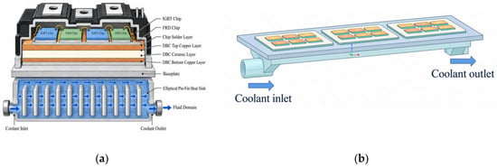
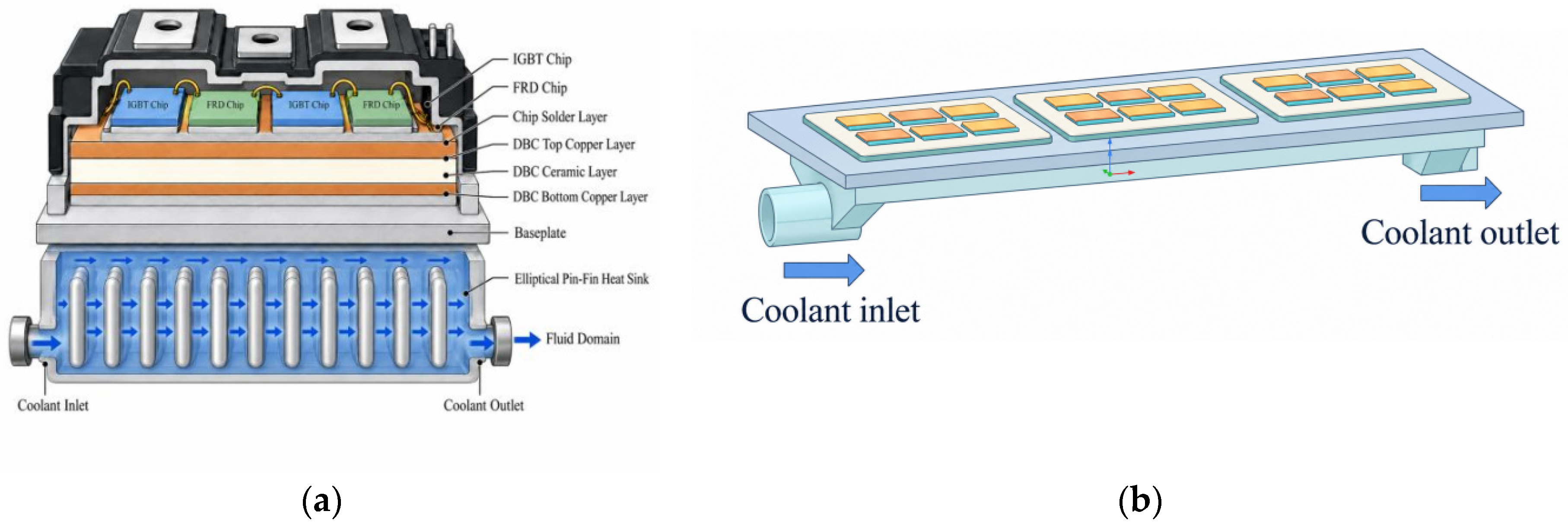
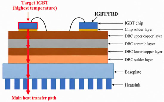
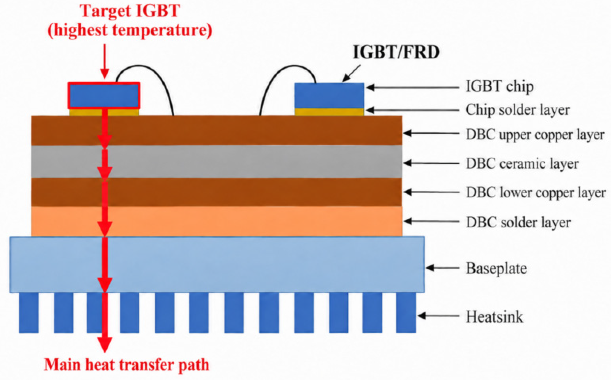
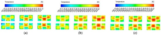
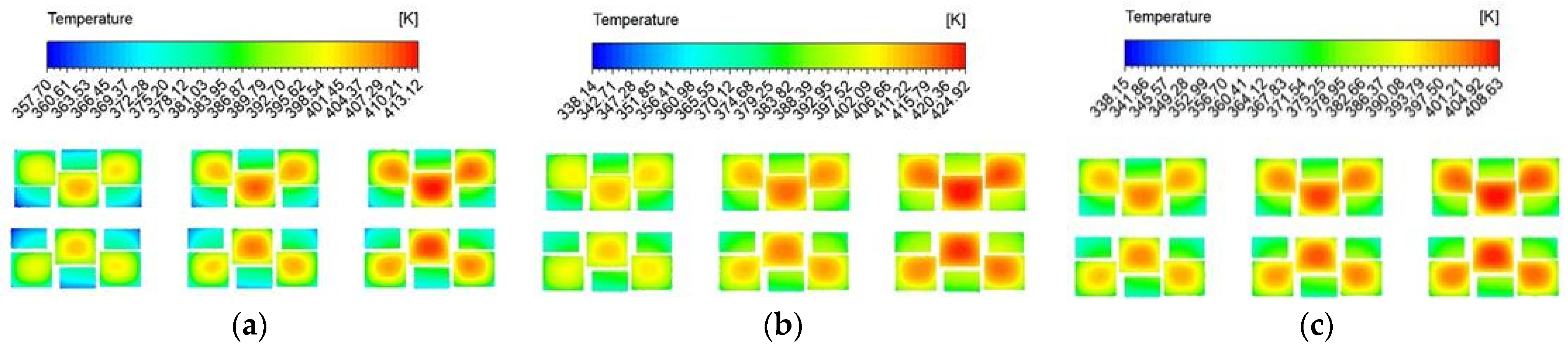
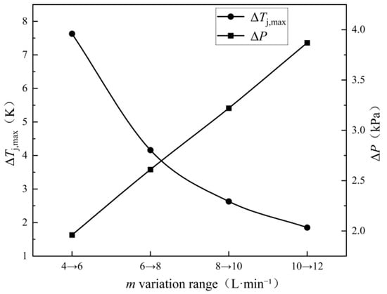
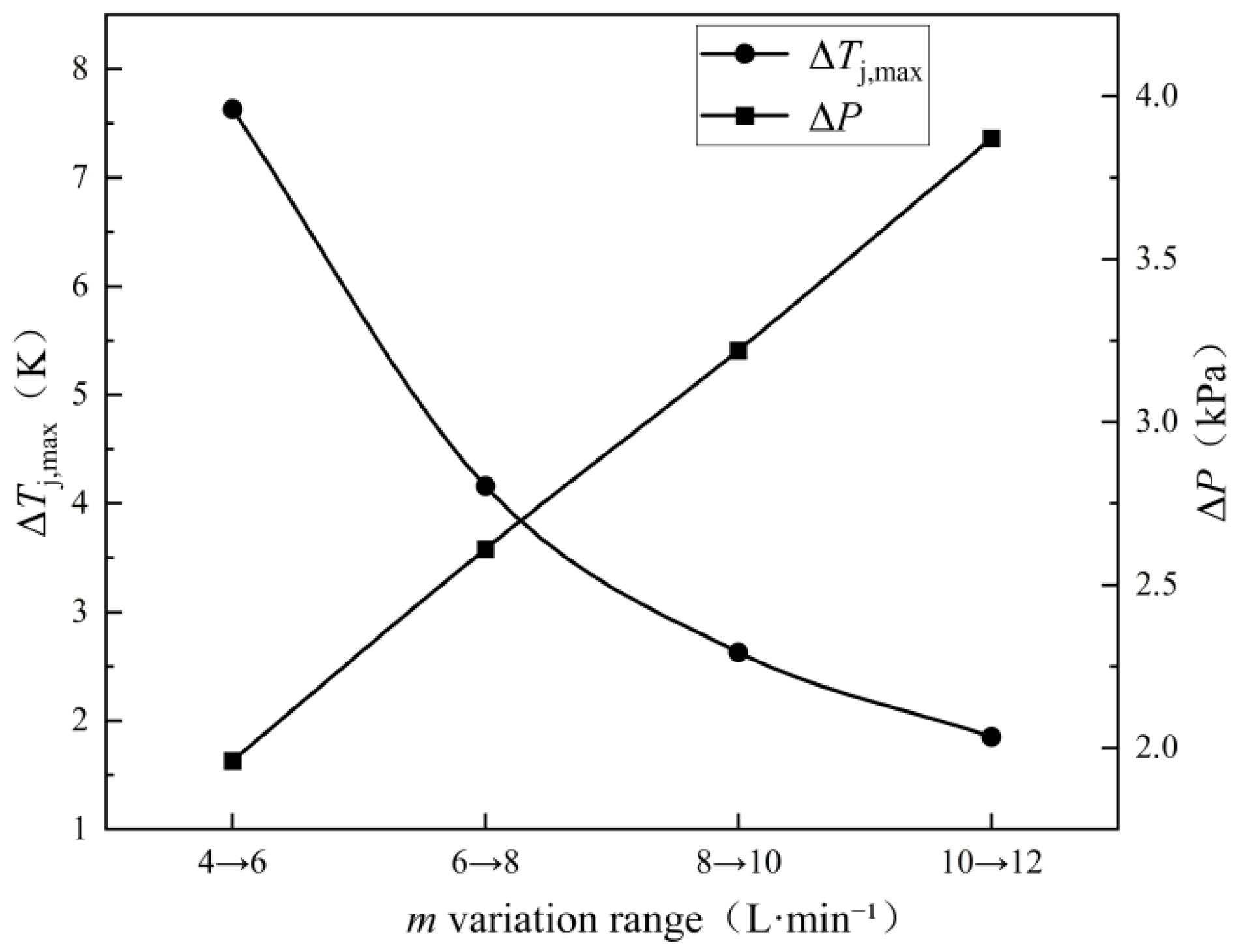
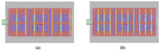
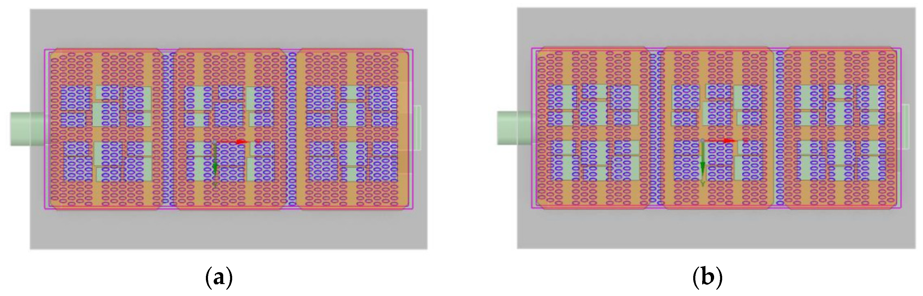
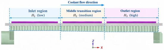
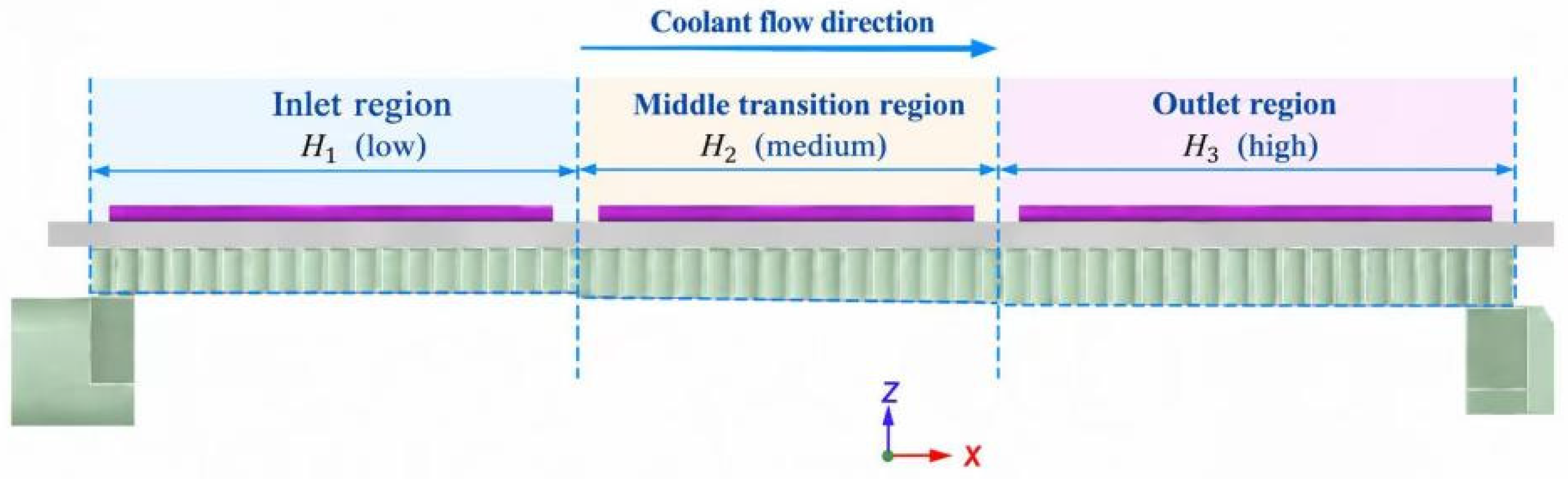
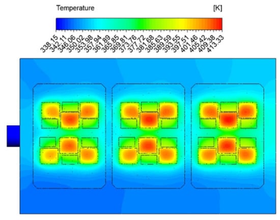
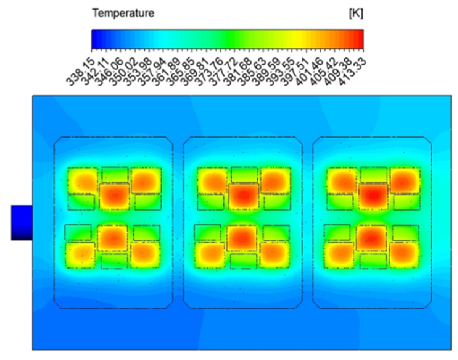
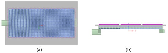
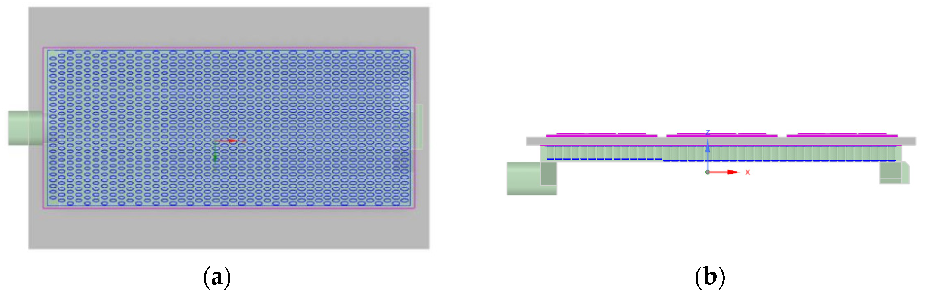
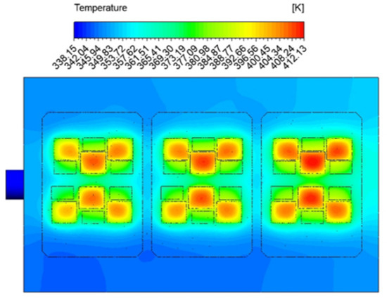
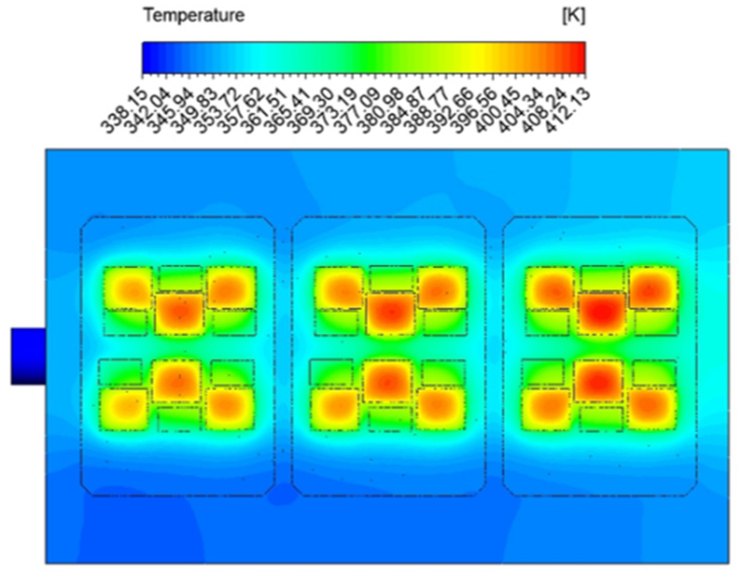
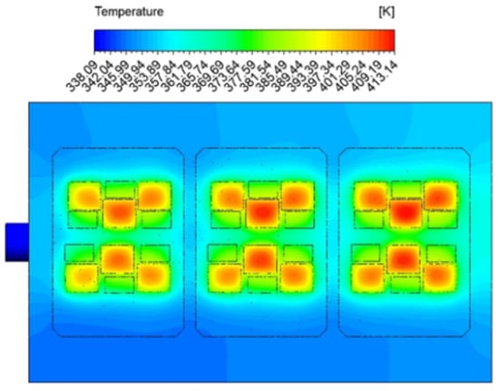
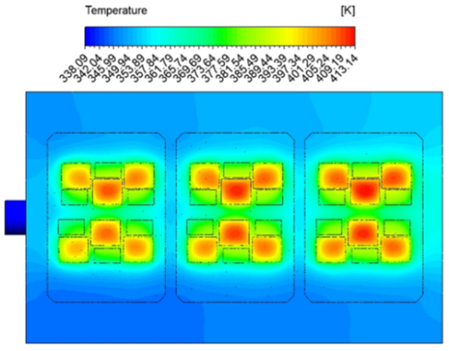
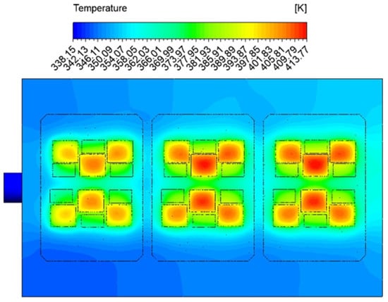
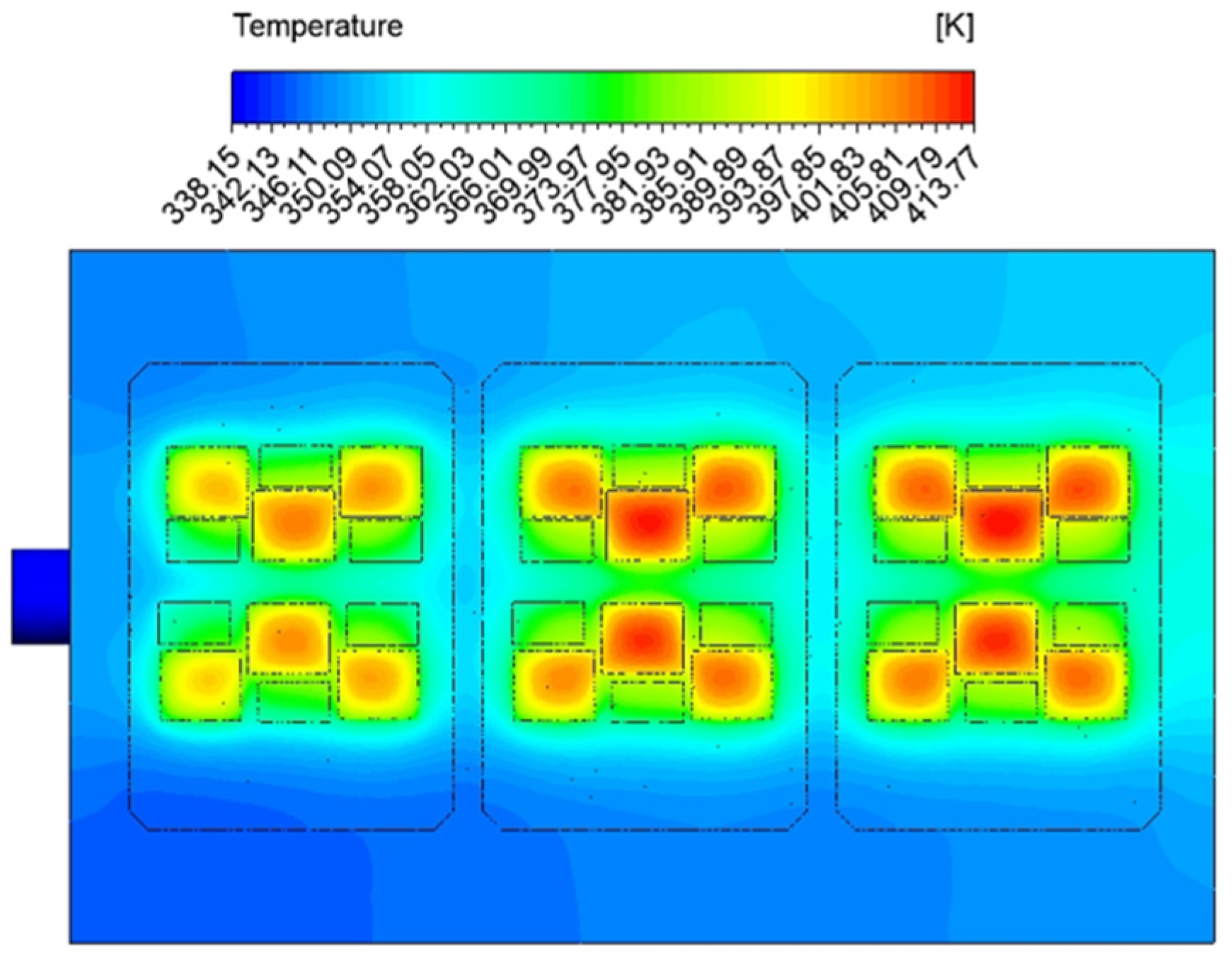
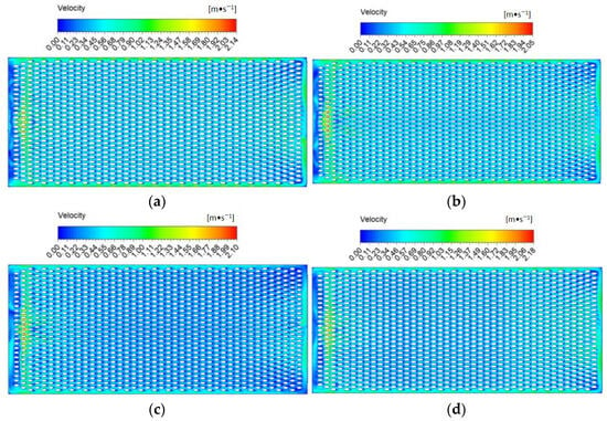
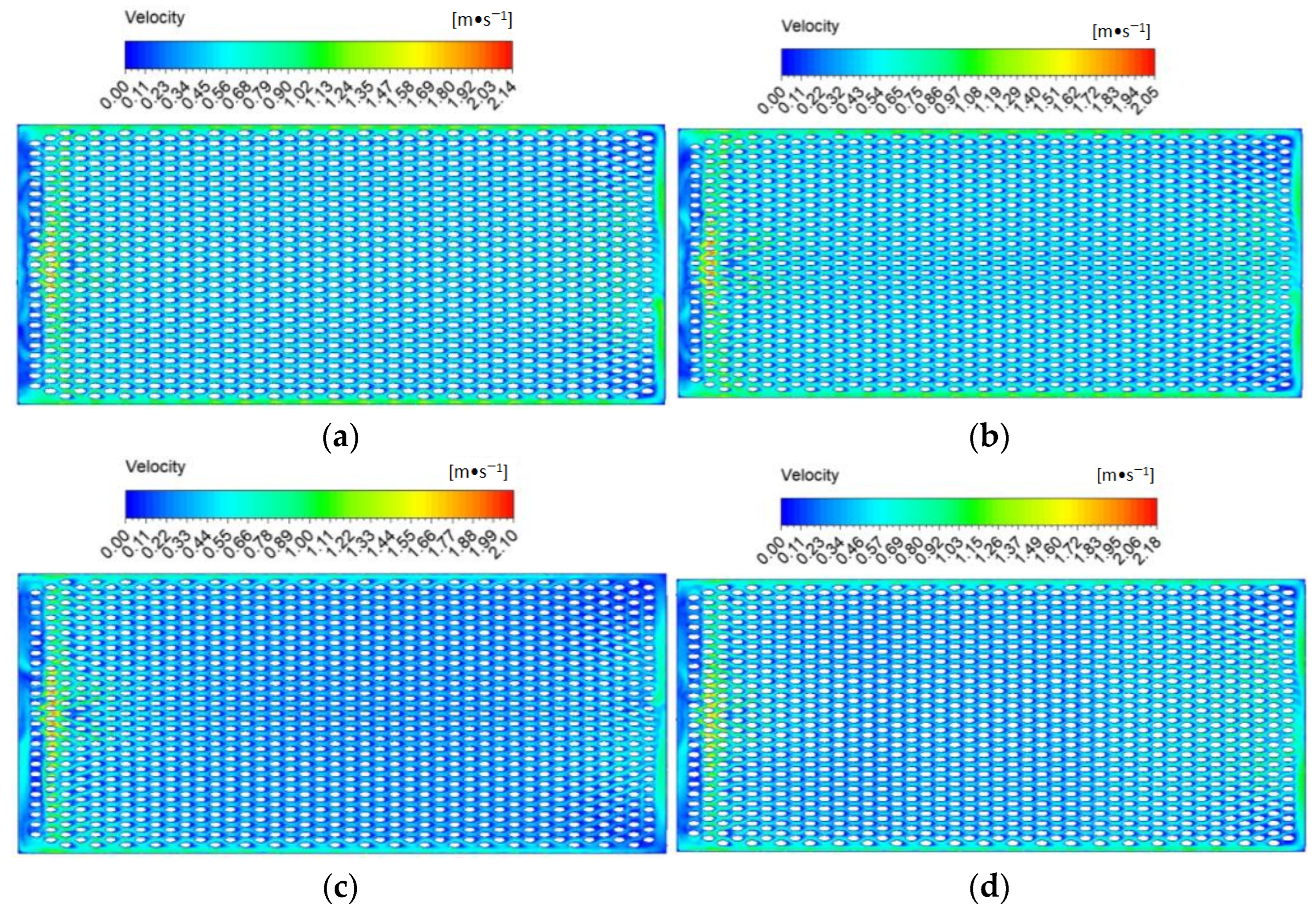
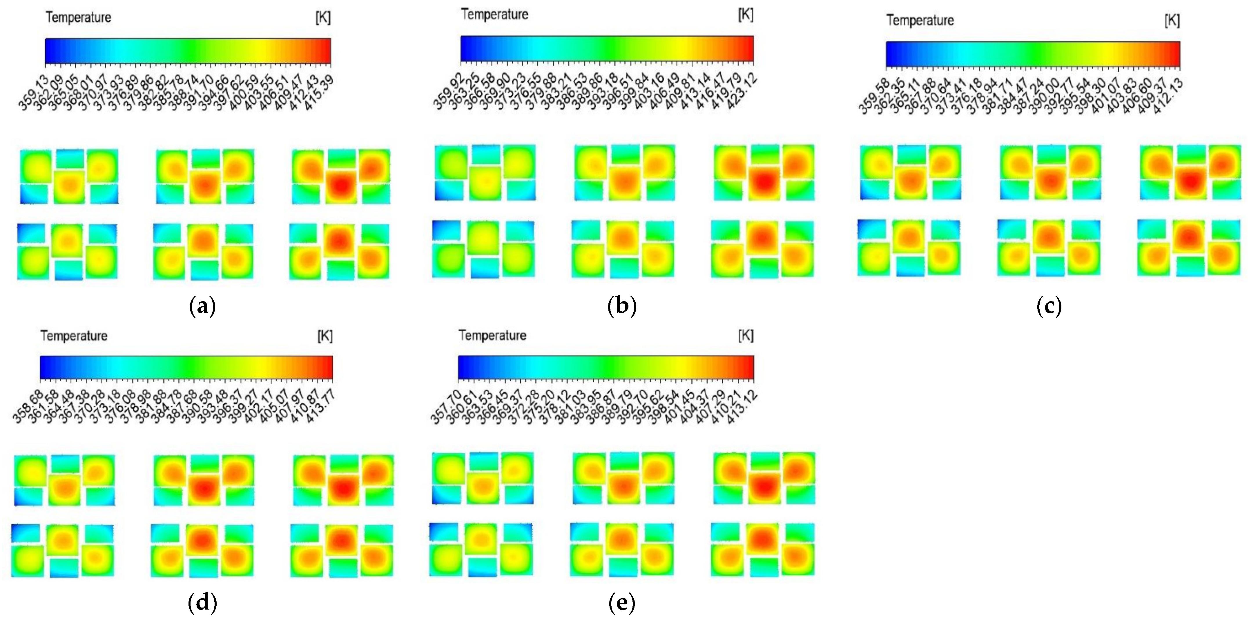

Disclaimer/Publisher’s Note: The statements, opinions and data contained in all publications are solely those of the individual author(s) and contributor(s) and not of MDPI and/or the editor(s). MDPI and/or the editor(s) disclaim responsibility for any injury to people or property resulting from any ideas, methods, instructions or products referred to in the content. |
© 2026 by the authors. Licensee MDPI, Basel, Switzerland. This article is an open access article distributed under the terms and conditions of the Creative Commons Attribution (CC BY) license.