


Featured Application
Low-voltage SEM with stage-bias modulation enables accurate characterization of pore structures in nonconductive polymer battery separators, providing a reliable tool for separator quality evaluation and failure analysis in lithium-ion batteries.
Abstract
Scanning electron microscopy (SEM) is a popular surface characterization technique. However, SEM observation and measurement of nonconducting soft materials still suffer from the charge effect and beam damage caused by high landing energy. In this work, a low-voltage SEM (LVSEM) was employed to directly observe and record the in situ beam damage of nonconducting polymer films. A series of unprecedented high-quality surface structure images of the nonconducting materials was obtained by controlling the landing energy of the incident electron beam.
1. Introduction
Electron microscopy has been widely used in the fields of material science [1,2,3,4], life science [5,6,7,8,9], semiconductors [10,11,12,13], and so on. Recently, electron microscopy applications were further expanded by advancements in aberration correction [14], cryo-electron microscopy [6,7,8,9], focused ion beam (FIB) [15,16], low-dose electron microscopy [1,2], high-sensitivity camera technology, and various in situ methods [17,18]. In particular, transmission electron microscopy (TEM) and scanning transmission electron microscopy (STEM) have been improved and seen increasing application scenarios due to their higher spatial resolution (<1 Å) [1,2] as compared with scanning electron microscopy (SEM, actual resolution ~2 nm) [19]. However, SEM has advantages compared to TEM or STEM; lower time cost, and it can be used to directly analyze a bulk sample without any preparation process.
SEM is a surface characterization technique that uses a focused electron beam to scan and radiate solid or quasi-solid materials and detect generated secondary electrons (SEs), backscattered electrons (BSEs), and characteristic X-rays, which provide surface topography, atomic number contrast, and elemental information, respectively [20]. Benefiting from high surface sensitivity and low time cost, SEM serves a variety of fields, including material science [21], semiconductors [22], and life science [23]. Different from the weak surface sensitivity of TEM and STEM, SEM can reveal detailed information on more microscopic surface structures [24]. When compared to scanning probe microscopy (SPM), SEM possesses the distinct advantage of low time cost [25]. However, SEM imaging of nonconducting soft materials still suffers from charging effects and beam damage caused by high-landing-energy incident electrons. In conventional wisdom, the high electron beam energy results in high resolution due to the short wavelength [26]. Meanwhile, the practical spatial resolution of SEM might be limited by the inclusion of delocalized secondary electron (SE2 and SE3) components [27]. In addition, SEM imaging inevitably faces challenges of the charging effect and beam damage with the high-voltage method. Low voltage coupled with an in-lens detector can control the signals dominated by the in situ component (SE1) which are emitted from a small escape depth under the specimen surface after direct excitation by the incident electron beam, as well as ease the charging on nonconducting materials and release the beam damage of soft materials.
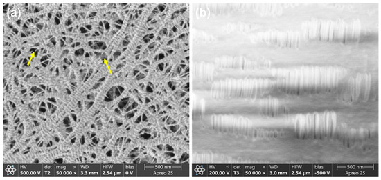
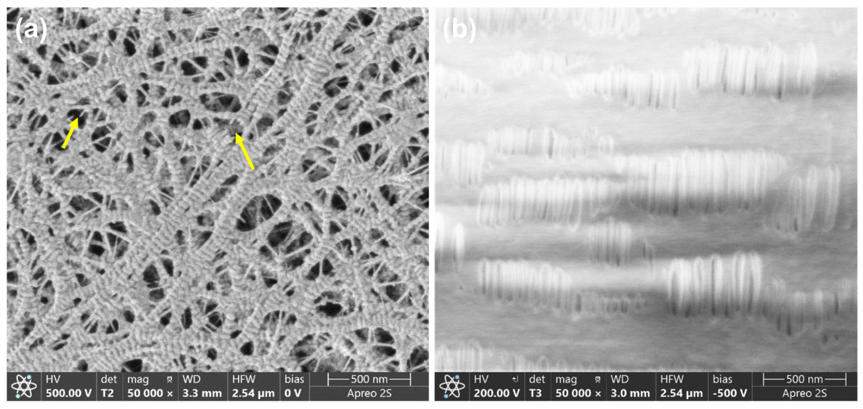
Nonconducting materials such as porous polymer films or mesoporous silica are widely used in energy and catalysis fields, for battery separators, confined reactions, and catalysts. Surface structure plays an important role in understanding the wettability and adsorption capacity of these materials. For battery separators, the essential function is electrical insulation, but porous structures enable ionic transport, whereas most separators are made of polyethylene (PE), polypropylene (PP), and their combinations [28]. These two factors present a challenge for SEM imaging. Beam sensitivity, the charging effect, and damage to the metal coating process can lead to various images (Figure 1) that provoke a misunderstanding of the relationship between structure and performance. To obtain effective SEM results, various factors should be considered. Here, the general requirements for SEM characterization should be summarized: (i) samples must be stable during the imaging process; (ii) the charging effect should be released with a certain strategy; (iii) the interactions between the incident electron beam and samples or the practical resolution should be considered for SEM imaging of sub 5 nm details on the surface.
Figure 1.
(a) LVSEM image of a commercial wet-process PE separator with ~2 nm Pt coating, (b) LVSEM image of a commercial dry-process PP separator (The yellow arrow indicates the area affected by the electron beam).
Unlike conventional SEM, which relies on high landing energies that induce irreversible thermal and structural damage in polyolefin separators, or low-dose cryo-SEM, which requires complex cryogenic sample preparation and specialized hardware, the approach presented here achieves damage-free imaging through a synergistic combination of ultra-low landing energy (100 eV) and a negative stage bias (−500 V). The stage bias decelerates the primary beam at the specimen surface, preserving the column’s optical performance while confining the excitation volume to the topmost polymer layer. Simultaneously, the retarding field suppresses delocalized SE2/SE3 contributions and mitigates surface charging without conductive coating. This configuration enables quantitative porosity measurement that aligns with bulk techniques (MIP and electrolyte uptake) while retaining the surface fidelity of AFM, offering a methodological advance for routine, high-throughput separator characterization without the time cost or environmental constraints of alternative approaches.
2. Materials and Methods
2.1. Materials
Two types of commercially available polymer separators, representative of the most widely used technologies in the lithium-ion battery industry, were investigated in this study. The dry-process separator was Celgard™ 2400 (Celgard, Charlotte, NC, USA), a monolayer polypropylene (PP) membrane. This material features a characteristic highly anisotropic, microporous structure generated through a sequence of extrusion, annealing, and uniaxial stretching. The wet-process separator was Hipore™ (Asahi Kasei Corp., Tokyo, Japan), a polyethylene (PE) membrane exhibiting a more isotropic, sponge-like porous network formed via thermally induced phase separation (TIPS).
These samples were selected specifically due to their high susceptibility to electron beam-induced thermal degradation and their distinct morphological differences. To ensure the characterization of the “native” surface state, the separators were used strictly in their as-received condition. No conductive coatings (such as gold or carbon) or chemical pre-treatments were applied, as these conventional preparation techniques can obscure nanometer-scale pore features or introduce structural artifacts through solvent–polymer interactions. The membranes were carefully mounted on aluminum stubs using conductive carbon adhesive tape, ensuring flat orientation to minimize topographical shading.
2.2. Low-Voltage SEM Characterization and In Situ Observation
All microscopic observations were performed using a Thermo Fisher Apreo 2S high-resolution field-emission scanning electron microscope (FE-SEM) (Waltham, MA, USA). To decouple the effects of beam energy and signal collection, the instrument was operated in retarding field mode (Stage Bias). The primary beam acceleration voltage and the negative stage bias were systematically adjusted to achieve various landing energies () ranging from 100 eV to 500 eV.
Imaging was conducted at a fixed working distance (WD) of 3.0–4.0 mm with a constant beam current of approximately 6.3–13 pA to minimize the total dose of injected electrons. Signal acquisition was primarily handled by the Trinity detection system, specifically utilizing the T1 (In-lens BSE) and T2 (In-lens SE) detectors to maximize surface sensitivity and spatial resolution. For in situ damage evolution studies, the beam was scanned continuously over a fixed region () at 500 eV, with frames captured at specific time intervals () to monitor the dynamic fusion of fibrils.
2.3. Image Processing and Quantitative Porosity Analysis
To ensure reproducibility and minimize operator bias, a standardized image analysis workflow was implemented using Fiji (ImageJ 1.54g) software. First, raw micrographs were calibrated by defining the spatial scale based on the image scale bar. Noise reduction was applied using a median filter (radius = 2 pixels) followed by a Gaussian blur () to suppress high-frequency artifacts without obscuring fibril edges. Pore segmentation was achieved via Otsu’s thresholding method, which automatically determines the optimal intensity cutoff to separate the dark pore regions from the bright polymer fibrils. The resulting binary mask was verified to ensure no pore bridging occurred. Surface porosity was then calculated as the area fraction of void spaces relative to the total analyzed area. To guarantee statistical reliability, porosity values were averaged from at least five distinct, non-overlapping regions of interest (ROIs) randomly selected from the sample surface for each experimental condition.
3. Results
3.1. Electron Signal Characteristics and Detection Configuration
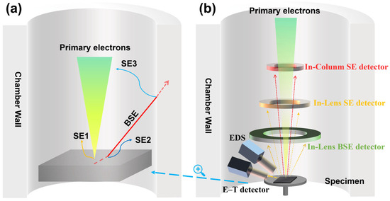
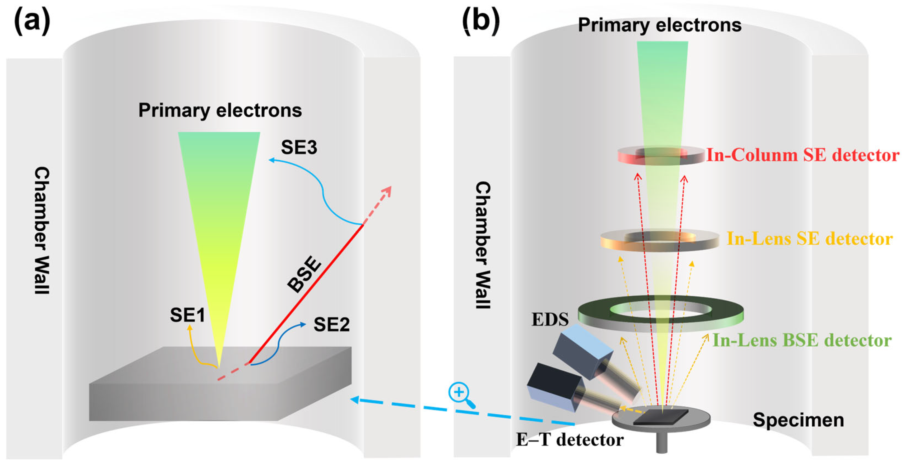
The precision of separator morphology characterization is fundamentally governed by the origin and collection efficiency of secondary electrons (SEs). As schematically illustrated in Figure 2a, when the primary electron (PE) beam interacts with the polymer matrix, three distinct categories of SEs are generated based on their excitation mechanisms. SE1 signals, emitted directly from the point of incidence, provide the highest spatial resolution. Due to their low kinetic energy (typically <50 eV), their escape depth is confined to a remarkably shallow near-surface region, typically within 1–2 nm [29]. This makes SE1 uniquely sensitive to the nanometer-scale fibrils and the sharp boundaries of the pores in polyolefin separators.
Figure 2.
(a) Sketch of the generated electron signals; (b) schematic of the detector system of a modern SEM.
In contrast, SE2 components are produced by backscattered electrons (BSEs) as they exit the specimen surface at some distance from the impact point. These signals carry delocalized topographic information and are influenced by the density and atomic number of the underlying material, often resulting in a “blurring” effect that obscures the true edges of the nanofibrils. SE3 signals further complicate the imaging process; they arise from BSEs striking the chamber walls or the objective lens pole piece, contributing solely to a non-informative background fog that reduces the overall image contrast.
To isolate the desirable SE1 signals, a specialized detector configuration is employed (Figure 2b). Conventional Everhart–Thornley (E-T) detectors, positioned at the side of the chamber, primarily collect SE2 and SE3 signals because they lack the geometric advantage to capture the axially emitted SE1. In contrast, the In-lens SE detector utilized in this study is positioned within the objective lens bore. It leverages the lens’s magnetic field to “snorkel” the low-energy SE1 electrons directly upward, significantly enhancing surface sensitivity [30]. By filtering out the delocalized SE2/SE3 contributions, this configuration allows for the clear visualization of the structure inherent to dry-process separators.
3.2. In Situ Beam Damage Evolution of PP Separator
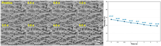
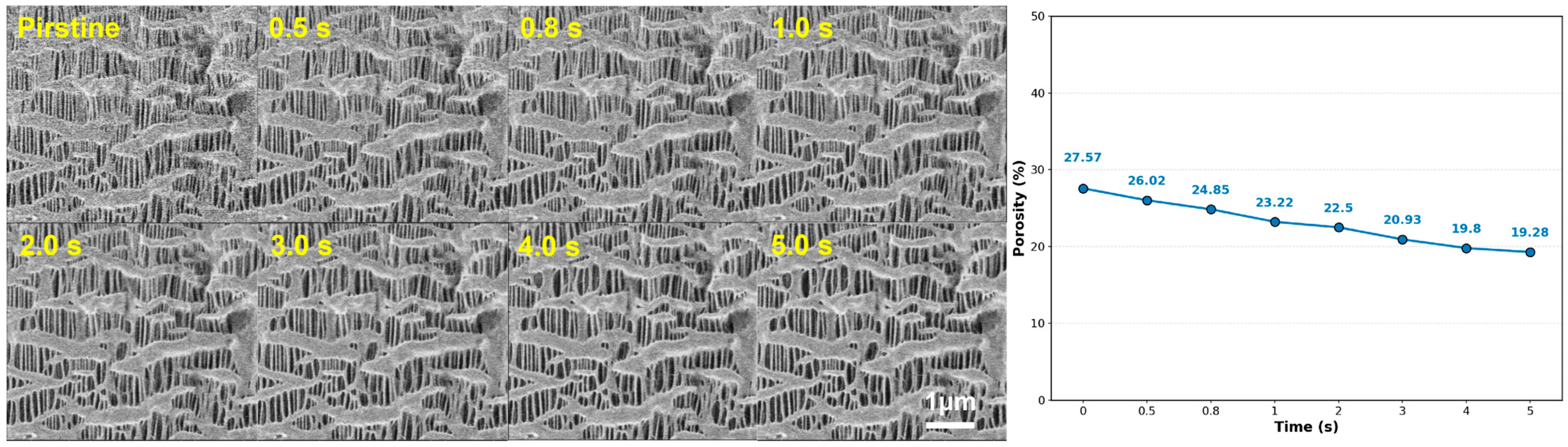
To establish a baseline for beam-induced artifacts, we performed an in situ time-resolved study on a Celgard-2400 PP separator at a moderate landing energy of 500 eV. Figure 3 captures the rapid structural metamorphosis of the polymer under continuous irradiation. At , the separator exhibits its native morphology, characterized by highly aligned, slender fibrils. However, as early as ~0.5 s, subtle softening and “thickening” of the fibrils become apparent. By 2.0 s, the slender fibrils begin to fuse at their junctions, a phenomenon driven by localized thermal accumulation.
Figure 3.
In situ beam damage process of a PP battery separator (500 eV). (Left) Images at different times. (Right) Porosity (processed using ImageJ).
Quantitative image analysis reveals a dramatic and monotonic decline in measured porosity during this brief exposure. The initial porosity of 27.54% (at ) plummets to 19.28% by . This reduction is accompanied by a distinct morphological transition: the originally high-aspect-ratio, slender pores gradually evolve into more thermodynamically stable elliptical or circular shapes.
This evolution is a classic manifestation of the “Heat Trap” effect. Polypropylene’s low thermal conductivity () prevents the efficient dissipation of the beam’s energy. As the local temperature exceeds the polymer’s and approaches its , the surface tension of the semi-molten polymer drives the contraction of the fibrils to minimize surface area. This results in the “necking” and eventual closure of the porous network, proving that conventional imaging durations at 500 eV inevitably lead to an underestimation of the separator’s transport properties.
3.3. Effect of Landing Energy and Stage Bias on Imaging
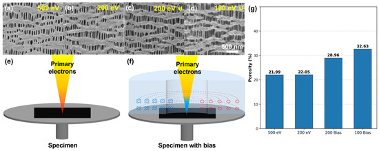
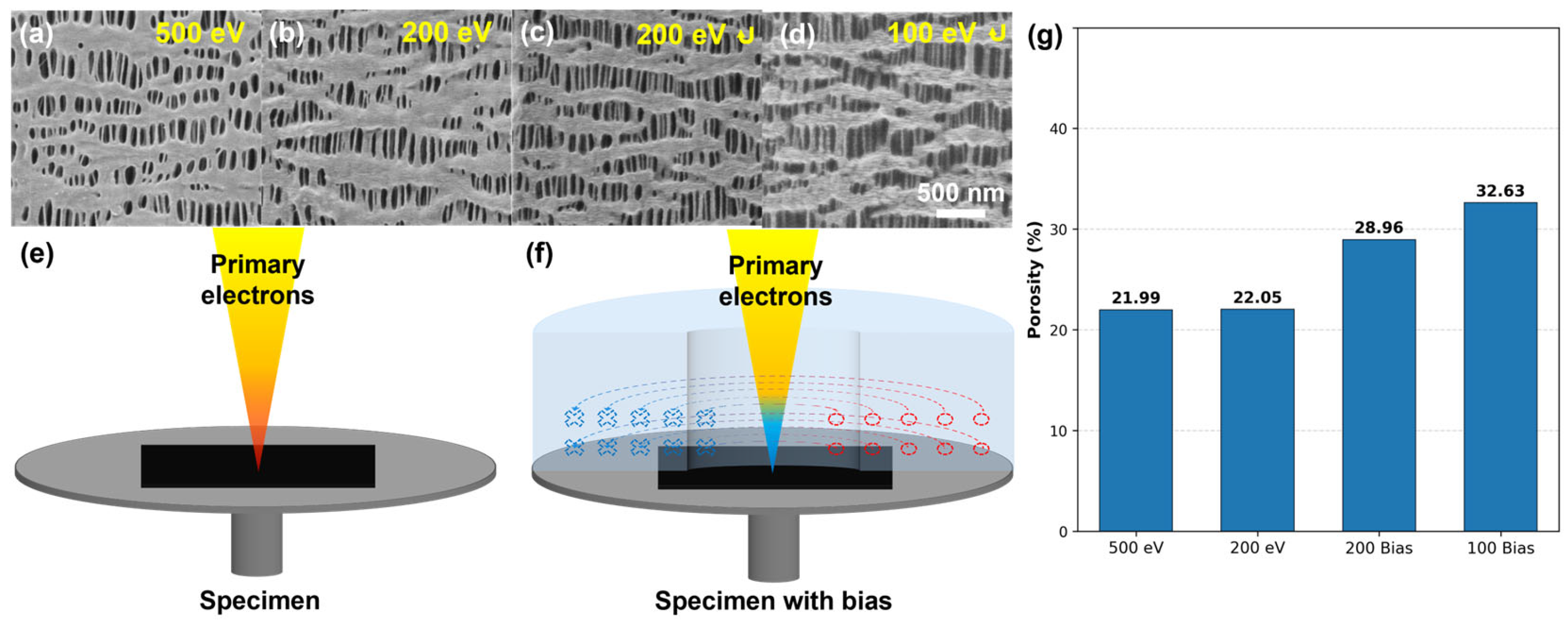
The interplay between landing energy (), surface charging, and image fidelity is explored in Figure 4. At a standard low-voltage setting of 500 eV (Figure 4a), the image exhibits a degree of “melted” appearance. The fibrils appear fused, and the pores are predominantly elliptical, yielding a calculated porosity of 21.98%. This value is consistent with several previous reports [31,32] that likely overlooked the immediate onset of beam damage.
Figure 4.
(a) SEM images of Celgard-2400 at 500 eV, (b) 200 eV, (c) 200 eV with −500 V stage bias, (d) 100 eV with −500 V stage bias, (e) schematic illustration of electron–specimen interaction during low-energy SEM imaging without stage bias, (f) schematic illustration of electron–specimen interaction during low-energy SEM imaging with stage bias applied. (g) The measurement of porosity under different acceleration voltages was carried out, and the results were statistically analyzed using ImageJ.
Reducing the landing energy to 200 eV (Figure 4b) succeeds in preserving a more slender fibril morphology, suggesting that the energy deposition rate is closer to the material’s damage threshold. However, a new challenge arises: surface charging. Without sufficient energy to penetrate or escape, electrons accumulate on the non-conductive PP surface, creating an electrostatic “fog” that reduces the three-dimensional (3D) stereoscopic contrast and blurs the edges [24].
The introduction of a −500 V negative stage bias at 200 eV (Figure 4c) marks a turning point. The bias establishes a retarding field that decelerates the primary beam while simultaneously accelerating the emitted SEs toward the In-lens detector. This “boost” significantly improves the signal-to-noise ratio (SNR) and sharpens the edges of the fibrils. Under these stabilized conditions, the measured porosity increases to ~28.95%, indicating that many previously “closed” pores are now visible.
The optimal imaging condition is achieved at 100 eV with a −500 V stage bias (Figure 4d). Here, the interaction volume is confined to the extreme surface layer, and the beam energy is far below the threshold for thermal fusion. The resulting image displays exceptional stereoscopic contrast, with well-defined, individual fibrils and a highly interconnected porous network. The porosity reaches a peak of ~32.63% [24,33]. Figure 4e,f illustrates the mechanism: without bias, low-energy electrons are trapped by surface potential barriers; with bias, the “immersion lens” effect ensures that even the lowest-energy SE1 signals are collected, providing a true representation of the separator’s topography.
3.4. Comparison with Other Characterization Methods
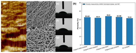
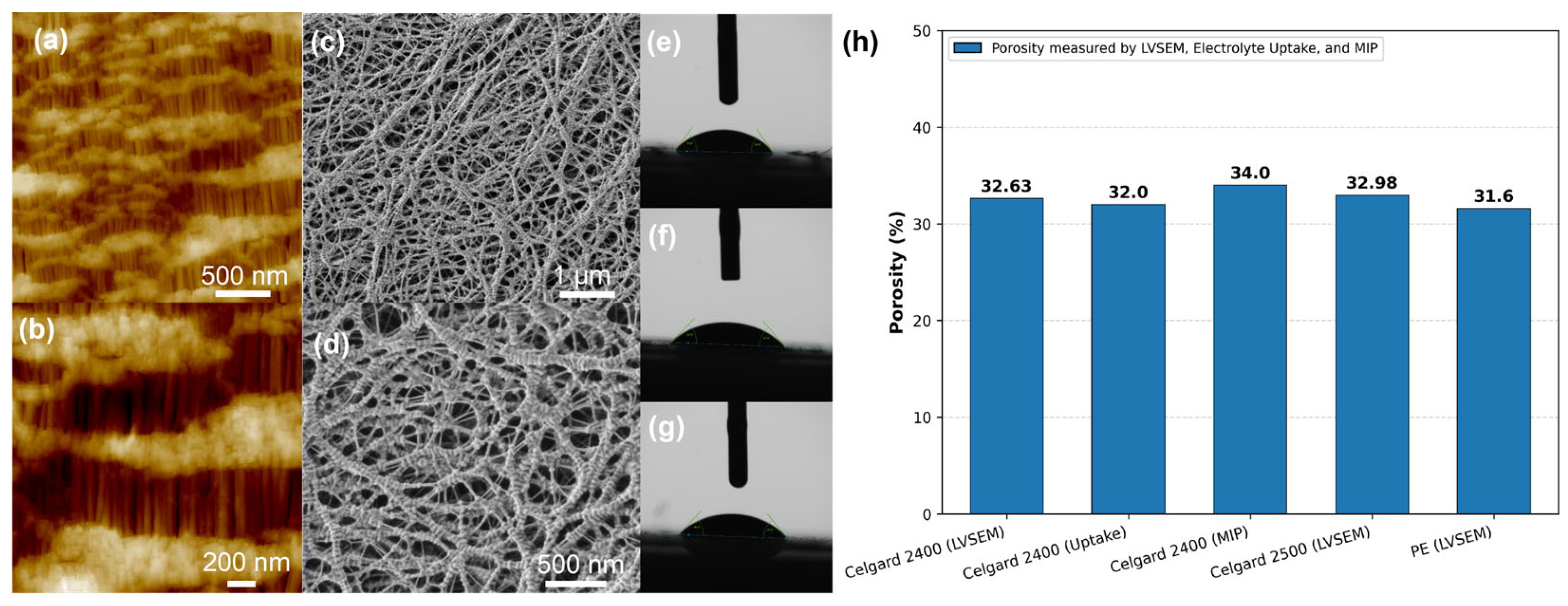
To validate the accuracy of our optimized LV-SEM method, the results were benchmarked against established independent techniques. As summarized in Figure 5, the porosity of ~32.63% obtained at 100 eV + Bias shows remarkable agreement with Mercury Intrusion Porosimetry (MIP) (~34%) and electrolyte uptake tests (~32%) [34]. While MIP provides a bulk average, our SEM method allows for the visualization of surface-specific pore distributions, which are critical for understanding lithium-ion flux at the electrode–separator interface.
Figure 5.
AFM images of Celgard 2400 at magnifications of (a) 50 k and (b) 100 k; LVSEM images of a wet-process PE separator at 200 V with magnifications of (c) 25 k and (d) 50 k; and contact angle test results with commercial electrolyte for (e) Celgard 2400 (~53.85°), (f) Celgard 2500 (~47.65°), and (g) wet-process PE separator (48.10°). (h) The porosity was measured using different methods.
Comparison with Atomic Force Microscopy (AFM) (Figure 5a–b) further confirms the morphological integrity. The fibril diameters and pore widths observed in AFM—a technique inherently free from electron beam damage—closely match our 100 eV SEM images. However, the SEM method offers a significantly larger field of view (FOV) and faster acquisition times, making it more suitable for statistical porosity analysis across large separator areas.
To demonstrate the versatility of this approach, we extended the characterization to other commercial separators. For the Celgard-2500 (a more porous dry-process PP) and a wet-process PE separator, the optimized method yielded porosities of ~32.98% and ~31.60%, respectively (Figure 5c–d). These structural findings are strongly correlated with the Contact Angle () measurements using commercial electrolytes (Figure 5e–g). The Celgard-2500 showed the lowest contact angle (~47.65°), consistent with its higher observed porosity and better wettability, while the wet-process PE exhibited a distinct “sponge-like” isotropic morphology compared to the uniaxial “shish-kebab” structure of the dry-process PP. By delivering porosity values consistent with MIP and electrolyte uptake tests while preserving the damage-free imaging fidelity of AFM, this method overcomes the low throughput of SPM and the lack of direct visualization in MIP, establishing a true “gold standard” for efficient and reliable separator analysis.
4. Discussion
4.1. Mechanism of Beam-Induced Damage
The characterization of polyolefin separators (PP/PE) in SEM involves a delicate balance between signal acquisition and specimen preservation. As illustrated in Figure 2a, the fundamental challenge lies in electron–polymer interactions. Secondary electrons (SE1), originating from the top 1–2 nm of the surface, are the only carriers of true nanometer-scale topographic information [29]. However, to generate these signals, the primary beam must penetrate the sample, leading to SE2 and SE3 production. SE2 signals, generated by backscattered electrons (BSEs) emerging from deeper regions, carry delocalized information that effectively “blurs” the sharp boundaries of the fibrils [35].
The structural collapse observed in our experiments is a “Thermo-Mechanical Coupling” process. Polymers like PP and PE have notoriously low thermal conductivity (). When high-energy electrons strike the porous network, the heat cannot dissipate through the narrow, suspended fibrils (the “heat trap” effect). The local temperature rise () can be described by the modified thermal diffusion model for porous media:
where is the beam power and is the fibril diameter. Since is in the nanometer range, even a pico-ampere current can drive the local temperature above the glass transition temperature () or even the melting point ( °C). Once , the polymer chains regain long-range mobility. The internal residual stresses, typically introduced during the uniaxial or biaxial stretching process of separator manufacturing, are suddenly released. This leads to the “necking” and “fusion” of fibrils, where the surface energy is minimized by shrinking the pores into elliptical or circular shapes [33]. Furthermore, radiolysis (chain scission) occurs as high-energy electrons break C–C bonds, reducing the molecular weight and further lowering the melting threshold of the material.
4.2. Influence of Electron Landing Energy
The extent of beam-induced damage is intrinsically linked to the interaction volume, which is a function of the electron landing energy () [26]. According to the Kanaya–Okayama range () formula, the penetration depth of electrons in a polymer is proportional to :
At 500 eV, the interaction volume extends tens of nanometers deep, encompassing multiple layers of the separator’s porous structure. This depth-integrated energy deposition causes subsurface melting, which manifests as a “sinking” of the surface pores. By reducing to 100 eV, we effectively confine the excitation volume to the “skin layer” of the separator.
However, low-energy imaging introduces the “low-voltage contrast paradox”: as energy decreases, the chromatic aberration of the objective lens increases, potentially degrading resolution [33]. Our results demonstrate that 100 eV is a “sweet spot” for polyolefins—high enough to generate sufficient SE1 for contrast, yet low enough to remain below the threshold for catastrophic thermal degradation. This energy level ensures that the measured pore dimensions represent the pristine state rather than a beam-modified artifact [24].
4.3. Role of Stage Bias in Charge Mitigation
The application of a negative stage bias () is not merely a method for charge suppression; it fundamentally alters the electron optics of the SEM. When a negative bias (e.g., −500 V) is applied to the sample, it creates a retarding field that decelerates the primary beam just before impact. This allows the primary electrons to travel through the column at higher energies (reducing chromatic aberration) while maintaining a low landing energy ().
More importantly, the stage bias creates an “Immersion Lens” effect [32]. The strong electrostatic field between the sample and the pole piece collimates the emitted secondary electrons, forcing them into the optical axis where they can be captured by the In-lens detector with nearly 100% efficiency. This mechanism selectively suppresses SE3 signals—which originate from BSE striking the chamber walls—thereby drastically increasing the signal-to-noise ratio (SNR).
For non-conductive separators, the bias also establishes a dynamic “Charge Balance”. In conventional SEM, surface charging creates an electrostatic “mirror” that deflects the beam. The negative stage bias “pushes” the accumulated surface electrons, promoting a stable secondary electron yield () where (where is the BSE yield). This equilibrium prevents the “blooming” effect at pore edges, allowing for the precise thresholding required for quantitative porosity analysis [24].
4.4. Accuracy of Porosity Measurement and Methodological Implications
The quantitative results of this study have significant implications for battery failure analysis and performance modeling. Traditional SEM characterization often involves metal coating (e.g., Au or Pt), which can clog pores smaller than 20 nm, or high-voltage imaging, which shrinks pores due to damage. Our data shows that these conventional methods can underestimate surface porosity by as much as 10–15%.
The high degree of correlation between our optimized LV-SEM method and Mercury Intrusion Porosimetry (MIP) or electrolyte uptake tests [36] confirms that the surface morphology captured at 100 eV + Bias is a faithful representation of the bulk properties. Unlike Atomic Force Microscopy (AFM), which provides excellent vertical resolution but a limited field of view, our method allows for multi-scale characterization—capturing thousands of pores in a single micro-graph for statistically significant analysis.
For the battery industry, the ability to observe the “true” pore structure is critical for calculating Tortuosity (), a key parameter in the MacMullin number (). Inaccurate porosity () measurements lead to errors in predicting ionic conductivity and Li-ion flux uniformity. Thus, the damage-free, non-coating approach proposed here provides a more reliable foundation for modeling fast-charging behaviors and dendrite growth resistance in next-generation high-energy-density batteries.
4.5. The Extended Application of This Method in Different Separator Systems
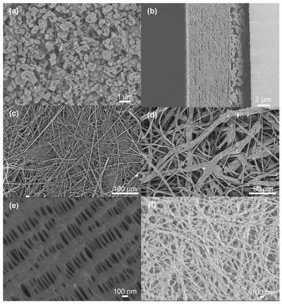
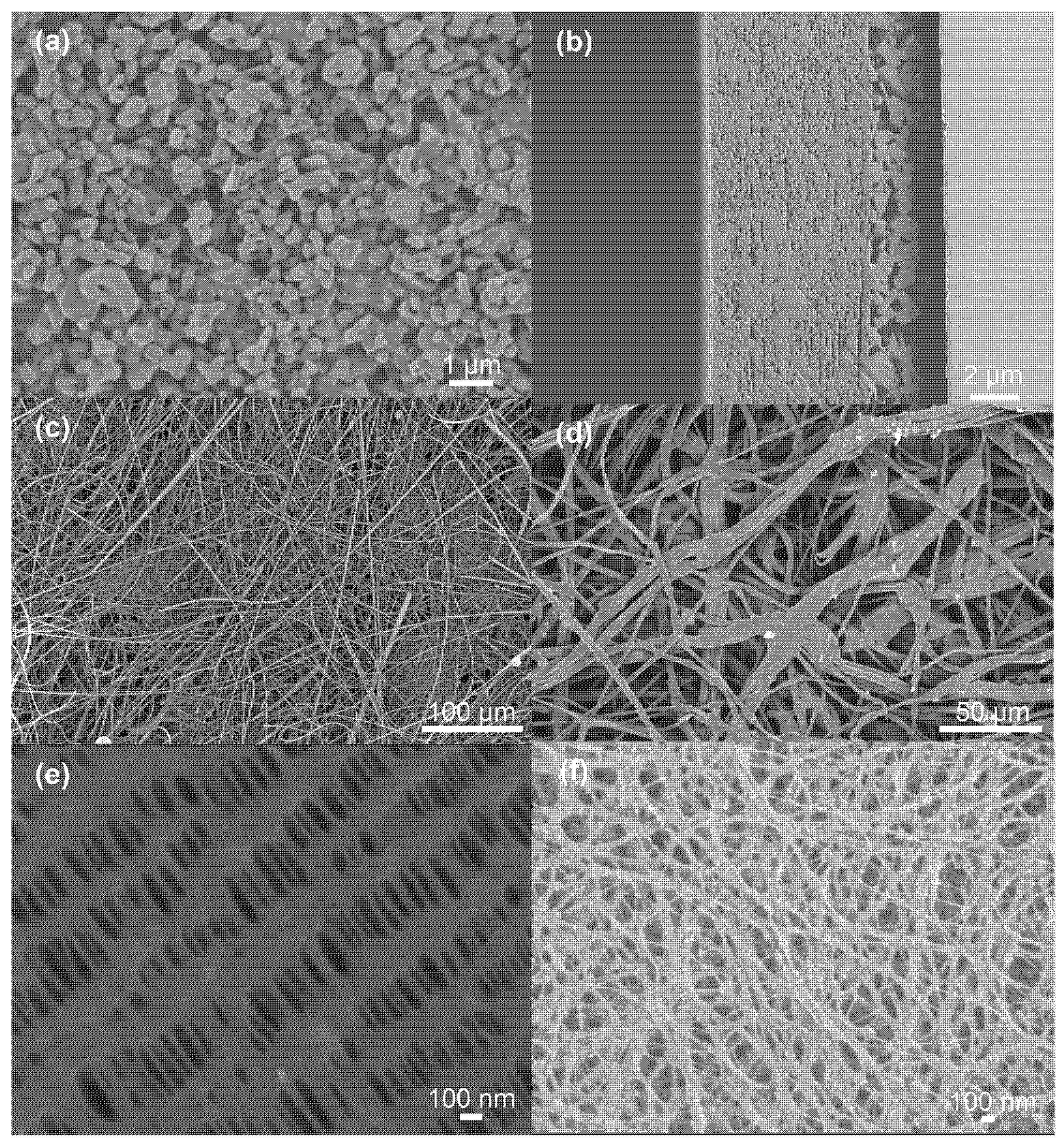
To evaluate broader applicability beyond PP/PE systems, the optimized protocol was extended to ceramic-coated, glass fiber, and cellulose acetate separators, as well as post-cycling samples (Figure 6). For non-polyolefin and hybrid materials, the 100 eV landing energy combined with stage bias effectively suppresses charging artifacts, allowing clear resolution of surface topography and coating–substrate interfaces without the delocalization typical of high-voltage imaging.
Figure 6.
Using the LVSEM + Stage Bias technique, observations were made on different materials. Ceramic diaphragm: (a) front view and (b) cross-section; glass fiber membrane: (c) cellulose acetate membrane, (d) Celgard-2400 after cycling, (e) Celgard-2400 after cycling, (f) wet-PE after cycling.
Regarding aged separators, the technique enables a clear distinction between rapid beam-induced artifacts and genuine cycling-induced degradation, such as fibril fracture and pore clogging. This capability is particularly valuable for post-mortem failure analysis, helping to isolate electrochemical wear from mechanical or thermal damage. To avoid complicating the issue and to eliminate the influence of other factors, we only compared the battery separators before and after the cycle. Our research subject was merely the issue of the electrolyte infiltration.
The method is best positioned as a comparative screening and quality control tool rather than for in situ analysis within sealed cells, due to vacuum and mounting constraints. It excels at manufacturing batch verification, pre-assembly material screening, and post-mortem examination. The consistent, damage-free imaging across diverse material classes confirms this approach as a robust, standardized framework for separator characterization.
5. Conclusions
In this study, we identified and quantified a critical limitation of conventional SEM in characterizing battery separators: the beam-induced “Heat Trap” effect, where electron irradiation triggers rapid thermal fusion of polymer fibrils, significantly underestimating true porosity. By systematically analyzing damage evolution, we established that this structural collapse is a thermo-mechanical process driven by localized energy deposition and the sudden release of residual manufacturing stresses.
To address this, we developed a damage-free characterization protocol combining ultra-low landing energy (100 eV) with a negative stage bias (−500 V). This approach effectively confines the excitation volume to the surface layer and eliminates charging artifacts without the need for conductive coating or cryogenic preparation. Crucially, the porosity values obtained under these optimized conditions show excellent agreement with independent bulk techniques, such as Mercury Intrusion Porosimetry (MIP) and electrolyte uptake tests, validating the method’s quantitative reliability.
Beyond methodological optimization, we demonstrated the versatility of this technique across diverse systems, including ceramic-coated, glass fiber, and post-cycling membranes. The ability to distinguish genuine electrochemical degradation features—such as pore clogging and SEI residue—from transient electron beam artifacts provides a robust tool for post mortem failure analysis. Collectively, this work establishes a standardized, non-destructive imaging framework that bridges the gap between qualitative morphology observation and quantitative performance modeling, offering significant advances for the evaluation and development of next-generation battery separators. Furthermore, the in situ damage evolution data recorded in this study provide essential experimental benchmarks for future reverse-imaging algorithms aimed at computationally reconstructing pristine morphology from beam-damaged states.
Author Contributions
L.W. and R.Z.: Investigation, conceptualization, characterization, data collection, and writing—original draft. Y.Y.: Conceptualization, validation, and data curation. Q.L.: Investigation, experimentalization, and data collection. X.F.: Data curation and supervision. Y.D.: Conceptualization, methodology, supervision, and writing—reviewing and editing. The manuscript was written through the contributions of all authors. All authors have read and agreed to the published version of the manuscript.
Funding
This research received no external funding.
Institutional Review Board Statement
Not applicable.
Informed Consent Statement
Not applicable.
Data Availability Statement
The original contributions presented in this study are included in the article. Further inquiries can be directed to the corresponding authors.
Conflicts of Interest
Author Yang Yu was employed by the company Carl Zeiss (Shanghai) Co., Ltd. Author Qin Luo was employed by the company Hitachi High-Tech (Shanghai) Co., Ltd. Author Xiaowei Fang was employed by the company Hefei Guojing Instrument Technology Co., Ltd. The remaining authors declare that the research was conducted in the absence of any commercial or financial relationships that could be construed as a potential conflict of interest.
Abbreviations
The following abbreviations are used in this manuscript:
| SEM | Scanning Electron Microscopy |
| LVSEM | Low-Voltage SEM |
| STEM | Scanning Transmission Electron Microscopy |
| SE | Secondary Electron |
| BSE | Backscattered Electron |
| PE | Polyethylene |
| PP | Polypropylene |
| SPM | Scanning Probe Microscopy |
| AFM | Atomic Force Microscopy |
References
- Shen, B.; Wang, H.; Xiong, H.; Chen, X.; Bosch, E.; Lazic, I.; Qian, W.; Wei, F. Atomic imaging of zeolite-confined single molecules by electron microscopy. Nature 2022, 607, 703–707. [Google Scholar] [CrossRef] [Scilit]
- Chen, H.; Wu, Z.; Ke, J.; Li, G.; Jiang, F.; Liu, Y.; Hong, M. Fabricating ultralow-power-excitable lanthanide-doped inorganic nanoparticles with anomalous thermo-enhanced photoluminescence behavior. Sci. China-Mater. 2022, 65, 2793–2801. [Google Scholar] [CrossRef] [Scilit]
- Sun, C.; Dong, W.; Yang, L.; Zuo, X.; Bao, L.; Hua, Z.; Chang, X.; Cai, R.; Chen, H.; Han, X.; et al. Anisotropic lithium-ion migration and electro-chemo-mechanical coupling in Sb2Se3 single crystals. Sci. China-Mater. 2022, 65, 2657–2664. [Google Scholar] [CrossRef] [Scilit]
- Wang, R.; Wang, Q.; Guo, H.; Chen, H. Monitoring the rapid nanocrystal transformation via trapped intermediates of silica encapsulation. Sci. China-Mater. 2022, 65, 1963–1970. [Google Scholar] [CrossRef] [Scilit]
- Guo, W.; Tan, L.; Li, Q.; Li, J.; Shang, L. Upconversion nanorods anchored metal-organic frameworks via hierarchical and dynamic assembly for synergistic therapy. Nano Res. 2022, 15, 7533–7541. [Google Scholar] [CrossRef] [Scilit]
- Peng, G.; Jin, H.; Liu, F.; Yang, X.; Sui, P.; Lin, S. Biomimetic ultrathin pepsomes for photo-controllable catalysis. Sci. China-Chem. 2022, 65, 2444–2449. [Google Scholar] [CrossRef] [Scilit]
- Sente, A.; Desai, R.; Naydenova, K.; Malinauskas, T.; Jounaidi, Y.; Miehling, J.; Zhou, X.; Masiulis, S.; Hardwick, S.; Chirgadze, D.; et al. Differential assembly diversifies GABAA receptor structures and signalling. Nature 2022, 604, 190–194. [Google Scholar] [CrossRef] [Scilit] [PubMed]
- Niu, Y.; Liu, R.; Guan, C.; Zhang, Y.; Chen, Z.; Hoerer, S.; Nar, H.; Chen, L. Structural basis of inhibition of the human SGLT2-MAP17 glucose transporter. Nature 2022, 601, 280–284. [Google Scholar] [CrossRef] [Scilit]
- Su, Z.; Zhang, K.; Kappel, K.; Li, S.; Palo, M.; Pintilie, G.; Rangan, R.; Luo, B.; Wei, Y.; Das, R.; et al. Cryo-EM structures of full-length Tetrahymena ribozyme at 3.1 Å resolution. Nature 2021, 596, 603–607. [Google Scholar] [CrossRef] [Scilit]
- Yan, Z.; Zhang, Z.; Wu, W.; Ji, X.; Sun, S.; Jiang, Y.; Tan, C.; Yang, L.; Chong, C.; Qiu, C.; et al. Floating solid-state thin films with dynamic structural colour. Nat. Nanotechnol. 2021, 16, 795–801. [Google Scholar] [CrossRef] [Scilit]
- Ma, K.; Zhang, L.; Jin, S.; Wang, Y.; Yoon, S.; Hwang, H.; Oh, J.; Jeong, D.; Wang, M.; Chatterjee, S.; et al. Epitaxial single-crystal hexagonal boron nitride multilayers on Ni (111). Nature 2022, 606, 88–93. [Google Scholar] [CrossRef] [Scilit]
- Wu, F.; Tian, H.; Shen, Y.; Hou, Z.; Ren, J.; Gou, G.; Sun, Y.; Yang, Y.; Ren, T. Vertical MoS2 transistors with sub-1-nm gate lengths. Nature 2022, 603, 259–264. [Google Scholar] [CrossRef] [Scilit]
- Xu, X.; Pan, Y.; Liu, S.; Han, B.; Gu, P.; Li, S.; Xu, W.; Peng, Y.; Han, Z.; Chen, J.; et al. Seeded 2D epitaxy of large-area single-crystal films of the van der Waals semiconductor 2H MoTe2. Science 2021, 372, 195–200. [Google Scholar] [CrossRef] [Scilit]
- Ishikawa, R.; Tanaka, R.; Morishita, S.; Kohno, Y.; Sawada, H.; Sasaki, T.; Ichikawa, M.; Hasegawa, M.; Shibata, N.; Ikuhara, Y. Automated geometric aberration correction for large-angle illumination STEM. Ultramicroscopy 2021, 222, 113215. [Google Scholar] [CrossRef] [Scilit]
- Buchnev, O.; Grant-Jacob, J.; Eason, R.; Zheludev, N.; Mills, B.; MacDonald, K. Deep-Learning-Assisted Focused Ion Beam Nanofabrication. Nano Lett. 2022, 22, 2734–2739. [Google Scholar] [CrossRef] [Scilit] [PubMed]
- Jehle, F.; Priemel, T.; Strauss, M.; Fratzl, P.; Bertinetti, L.; Harrington, M. Collagen Pentablock Copolymers Form Smectic Liquid Crystals as Precursors for Mussel Byssus Fabrication. Acs Nano 2021, 15, 6829–6838. [Google Scholar] [CrossRef] [Scilit] [PubMed]
- Zhang, J.; Li, G.; Liao, H.; Sun, S. Tracking the atomic pathways of Pt3Ni-Ni(OH)2 core-shell structures at the gas-liquid interface by in-situ liquid cell TEM. Sci. China-Chem. 2020, 63, 513–518. [Google Scholar] [CrossRef] [Scilit]
- Cui, J.; Zheng, H.; He, K. In Situ TEM Study on Conversion-Type Electrodes for Rechargeable Ion Batteries. Adv. Mater. 2021, 33, 2000699. [Google Scholar] [CrossRef] [Scilit] [PubMed]
- Tüysüz, H.; Lehmann, C.; Bongard, H.; Tesche, B.; Schmidt, R.; Schüth, F. Direct imaging of surface topology and pore system of ordered mesoporous silica (MCM-41, SBA-15, and KIT-6) and nanocast metal oxides by high resolution scanning electron microscopy. J. Am. Chem. Soc. 2008, 130, 11510–11517. [Google Scholar] [CrossRef] [Scilit] [PubMed]
- Hidalgo, J.; Castro-Méndez, A.; Correa-Baena, J. Imaging and Mapping Characterization Tools for Perovskite Solar Cells. Adv. Energy Mater. 2019, 9, 1900444. [Google Scholar] [CrossRef] [Scilit]
- Jiang, L.; van Deursen, P.; Arjmandi-Tash, H.; Belyaeva, L.; Qi, H.; He, J.; Kofman, V.; Wu, L.; Muravev, V.; Kaiser, U.; et al. Reversible hydrogenation restores defected graphene to graphene. Sci. China-Chem. 2021, 64, 1047–1056. [Google Scholar] [CrossRef] [Scilit]
- Shen, Y.; Yu, H.; Xu, T.; Zhang, Q.; Yin, K.; Cong, S.; Liu, Y.; Sun, L. Tailoring Bi2Te3 edge with semiconductor and metal properties under electron beam irradiation. Nano Res. 2022, 15, 4710–4716. [Google Scholar] [CrossRef] [Scilit]
- Haridy, Y.; Osenberg, M.; Hilger, A.; Manke, I.; Davesne, D.; Witzmann, F. Bone metabolism and evolutionary origin of osteocytes: Novel application of FIB-SEM tomography. Sci. Adv. 2021, 7, eabb9113. [Google Scholar] [CrossRef] [Scilit] [PubMed]
- Modena, M.; Ruhle, B.; Burg, T.; Wuttke, S. Nanoparticle Characterization: What to Measure? Adv. Mater. 2019, 31, e1901556. [Google Scholar] [CrossRef] [Scilit] [PubMed]
- Kalinin, S.; Dyck, O.; Balke, N.; Neumayer, S.; Tsai, W.; Vasudevan, R.; Lingerfelt, D.; Ahmadi, M.; Ziatdinov, M.; McDowell, M.; et al. Toward Electrochemical Studies on the Nanometer and Atomic Scales: Progress, Challenges, and Opportunities. ACS Nano 2019, 13, 9735–9780. [Google Scholar] [CrossRef] [Scilit] [PubMed]
- Hwang, S.; Chen, X.; Zhou, G.; Su, D. In Situ Transmission Electron Microscopy on Energy-Related Catalysis. Adv. Energy Mater. 2020, 10, 1902105. [Google Scholar] [CrossRef] [Scilit]
- Zhang, X.; Cen, X.; Ravichandran, R.; Hughes, L.; van Benthem, K. Simultaneous Scanning Electron Microscope Imaging of Topographical and Chemical Contrast Using In-Lens, In-Column, and Everhart-Thornley Detector Systems. Microsc. Microanal. 2016, 22, 565–575. [Google Scholar] [CrossRef] [Scilit]
- Lagadec, M.; Zahn, R.; Wood, V. Characterization and performance evaluation of lithium-ion battery separators. Nat. Energy 2019, 4, 16–25. [Google Scholar] [CrossRef] [Scilit]
- Cazaux, J. From the physics of secondary electron emission to image contrasts in scanning electron microscopy. J. Electron Microsc. 2012, 61, 261–284. [Google Scholar] [CrossRef] [Scilit]
- Zhou, W.; Apkarian, R.; Wang, Z.L.; Joy, D. Fundamentals of Scanning Electron Microscopy (SEM). In Scanning Microscopy for Nanotechnology: Techniques and Applications; Zhou, W., Wang, Z.L., Eds.; Springer: New York, NY, USA, 2006. [Google Scholar]
- Wang, J.; Cai, W.; Mu, X.; Han, L.; Wu, N.; Liao, C.; Kan, Y.; Hu, Y. Designing of multifunctional and flame retardant separator towards safer high-performance lithium-sulfur batteries. Nano Res. 2021, 14, 4865–4877. [Google Scholar] [CrossRef] [Scilit]
- Deng, Y.; Pan, Y.; Zhang, Z.; Fu, Y.; Gong, L.; Liu, C.; Yang, J.; Zhang, H.; Cheng, X. Novel Thermotolerant and Flexible Polyimide Aerogel Separator Achieving Advanced Lithium-Ion Batteries. Adv. Funct. Mater. 2022, 32, 2106176. [Google Scholar] [CrossRef] [Scilit]
- Yuan, P.; Wu, J.; Ogletree, D.; Urban, J.; Dames, C.; Ma, Y. Adapting the Electron Beam from SEM as a Quantitative Heating Source for Nanoscale Thermal Metrology. Nano Lett. 2020, 20, 3019–3029. [Google Scholar] [CrossRef] [Scilit]
- Suga, M.; Asahina, S.; Sakuda, Y.; Kazumori, H.; Nishiyama, H.; Nokuo, T.; Alfredsson, V.; Kjellman, T.; Stevens, S.; Cho, H.; et al. Recent progress in scanning electron microscopy for the characterization of fine structural details of nano materials. Prog. Solid State Chem. 2014, 42, 1–21. [Google Scholar] [CrossRef] [Scilit]
- Kumagai, K.; Sekiguchi, T. Sharing of secondary electrons by in-lens and out-lens detector in low-voltage scanning electron microscope equipped with immersion lens. Ultramicroscopy 2009, 109, 368–372. [Google Scholar] [CrossRef] [Scilit]
- Abraham, K. Driections in secondary lithium battery research-and-development. Electrochim. Acta 1993, 38, 1233–1248. [Google Scholar] [CrossRef] [Scilit]
Disclaimer/Publisher’s Note: The statements, opinions and data contained in all publications are solely those of the individual author(s) and contributor(s) and not of MDPI and/or the editor(s). MDPI and/or the editor(s) disclaim responsibility for any injury to people or property resulting from any ideas, methods, instructions or products referred to in the content. |
© 2026 by the authors. Licensee MDPI, Basel, Switzerland. This article is an open access article distributed under the terms and conditions of the Creative Commons Attribution (CC BY) license.