


Abstract
In response to the issues associated with implementing cryptographic algorithms using the traditional hardware description language Verilog Hardware Description Language (Verilog HDL)—namely, high code complexity, long development cycles, and difficult debugging—this paper proposes a hardware implementation scheme for the lightweight block cipher algorithm Midori-128 based on the Chisel language. This scheme adopts an iterative structure and optimizes the algorithm for throughput. The algorithm has been successfully deployed on both Xilinx platforms and the domestically produced PGL100H platform, and a power consumption analysis has been completed. Compared to traditional Verilog implementations, this design delivers a throughput improvement of approximately 42.5% on the Virtex-5 platform and approximately 124.63% on the Spartan-6 platform. It maintains lightweight logic resource utilization and excellent cross-platform adaptability, making it suitable for resource-constrained embedded security applications and providing efficient, independently controllable cryptographic hardware support. Furthermore, the design fully preserves the symmetric cryptographic properties of Midori-128.
1. Introduction
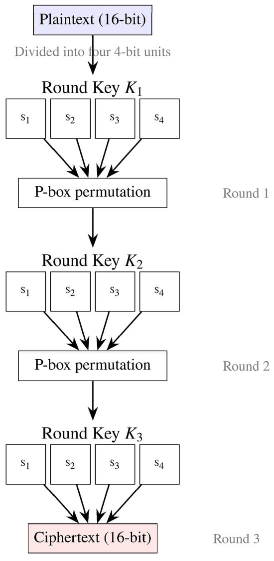
With the large-scale deployment of the Internet of Things (IoT), edge computing, and smart embedded devices [1], various resource-constrained endpoints—such as microcontrollers and RFID tags—are widely used in scenarios including industrial monitoring, smart homes and medical wearables [2]. Such devices impose stringent requirements on the security of data transmission and storage [3,4]. While AES [5] and DES [6,7] are well-established and perform well in software environments, their hardware implementations on resource-constrained platforms often suffer from high computational complexity, excessive hardware resource consumption, and significant power dissipation [8]. Consequently, they struggle to meet the security requirements of low power consumption, small footprint and high cost-effectiveness in resource-constrained scenarios [9], becoming a key bottleneck constraining the secure deployment of IoT endpoints. To address this issue, lightweight cryptography has emerged. Current research focuses on reducing the hardware footprint, power consumption and computational speed of cryptographic algorithms [10,11], striving to achieve a reasonable balance between algorithms and resource-constrained devices. The Midori lightweight block cipher algorithm is a prime example of this research. This cryptographic algorithm was proposed by Subhadeep Banik [12] and colleagues in 2015. Designed as a block cipher for low-power scenarios, Midori offers two block sizes: 64-bit and 128-bit [13], namely Midori-64 and Midori-128. Both variants utilize a 128-bit master key length [14], thereby ensuring the security of the key space while maintaining the algorithm’s flexibility [15]. The algorithm as a whole adopts the classic Substitution Permutation Network (SPN) structure found in block ciphers [16] (see Figure 1), whilst incorporating several targeted innovations and optimisations in its underlying implementation. Compared to traditional SPN-based ciphers, the Midori algorithm introduces energy-optimized S-boxes, effectively reducing signal delay in hardware circuits and the energy consumption associated with logic gate switching [17]. It also incorporates a lightweight modification to the MixColumns operation and further reduces the hardware implementation cost and energy consumption of the algorithm by simplifying the matrix operation logic, making it one of the preferred algorithms for secure encryption in resource-constrained scenarios. We assume a passive attacker model with eavesdropping only, suitable for low-cost IoT endpoints. Formal cryptanalysis and side-channel resistance are not evaluated in this work, as the focus is on hardware implementation and performance optimization.
Figure 1.
SPN structure.
Chisel, a hardware construction language based on the Scala programming language [18], is a new type of hardware description tool designed for modern digital circuit design. Its core design objectives are to simplify the development process for complex hardware systems and to enhance design efficiency and code maintainability [19]. It is widely applicable to the design and implementation of complex digital circuits such as microprocessors, cryptographic circuits and digital signal processing modules [20]. Compared with Verilog HDL, Chisel combines the flexibility of software programming with the rigor of hardware design, demonstrating significant advantages in terms of code conciseness, module reusability and parametric design capabilities. As Chisel is embedded within the Scala language, designers can leverage Scala’s object-oriented features to encapsulate, inherit and implement polymorphism in hardware modules in much the same way as when writing software programs, thereby achieving efficient reuse of hardware code. Furthermore, its support for parametric design enables rapid adaptation to different hardware platforms and functional requirements [21], significantly reducing repetitive development work [22].
To date, there have been numerous research findings regarding hardware optimizations for the Midori algorithm. Among these, optimizations for Midori-64 have yielded favorable results. For instance, Feng Jingya [23] addressed the design challenges of the Midori-64 hardware architecture by logically integrating the whitening key addition and round key addition operations, and utilizing multiplexers to optimize component reuse. They proposed a novel iterative hardware architecture. This design achieved a high throughput of 1300.74 Mbps on the Xilinx Spartan-6 FPGA platform, fully demonstrating the potential for hardware optimisation of the Midori algorithm. In contrast, research into hardware implementations of the Midori-128 algorithm still has significant room for optimisation. For instance, the Midori-128 iterative hardware architecture designed by Lara-Nino [13] achieved a throughput of only 381 Mbps on the same Xilinx Spartan-6 FPGA platform, with hardware resource utilization and performance yet to reach optimal levels. Consequently, this paper proposes a Chisel-based hardware implementation scheme for the Midori-128 lightweight block cipher algorithm. By fully leveraging the design advantages of the Chisel language and the characteristics of the Midori-128 cipher algorithm, the scheme achieves a maximum throughput of 820.51 Mbps.
Specifically, the contributions of this paper are as follows:
- A lightweight cryptographic algorithm based on the Chisel language was implemented, effectively improving the algorithm’s throughput and operational efficiency; a comprehensive comparison and analysis was then carried out with existing research findings.
- In the Chisel language, a parametric design mechanism enables a single set of hardware logic to support both the Midori-64 and Midori-128 algorithm variants. The core encryption operations of the Midori-128 algorithm are divided into independent, reusable modular hardware units, thereby achieving decoupled design and flexible invocation of each functional module.
- A finite state machine design based on the Chisel language is proposed to precisely control the timing and logic of the 20-round encryption algorithm. Furthermore, a comprehensive simulation and verification environment is established using the ChiselTest framework to enable end-to-end functional simulation and logical verification of the encryption algorithm.
- We conducted innovative multi-platform comparative experiments using the domestically developed EDA tool Pango Design Suite and the Xilinx series development environment. We completed the synthesis, placement and routing, and performance testing of the Midori-128 hardware implementation, and systematically evaluated and compared key performance metrics—such as hardware resources, operating frequency and throughput—across different platforms.
- The algorithms were implemented using Chisel and Verilog, and a comparative analysis of these two development approaches was carried out.
The remainder of this paper is structured as follows. Section 2 provides a detailed description of the Midori block cipher algorithm. The hardware implementation architecture of the algorithm is described in Section 3. Section 4 presents experimental results obtained on various FPGA platforms and provides a comparative analysis with the published literature. Finally, Section 5 summarizes the paper.
2. Introduction to Midori Group Cipher Algorithm
As a typical lightweight block cipher algorithm designed for resource-constrained environments, Midori employs the well-established SPN structure in cryptography [24]. The algorithm offers two flexible variants to meet the security requirements of different scenarios: Midori-64, with a 64-bit block size, and Midori-128, with a 128-bit block size. Both variants utilize a fixed 128-bit master key length, a design that ensures the algorithm possesses a sufficient key space.
Apart from the core difference in block size, the two versions of Midori also feature adaptive designs in key parameters such as the number of encryption rounds; Midori-64 uses 4-byte blocks as its basic operation unit, with the encryption process requiring 16 rounds of iteration. Midori-128, on the other hand, uses 8-bit bytes as its operational unit, corresponding to 20 rounds of encryption, compensating for the security strength requirements imposed by the 128-bit block size through an increased number of rounds. The parameters of the Midori algorithm across different versions are shown in Table 1.
Table 1.
Midori algorithm parameters.
Midori uses two double-target 4-bit S-boxes [25], Sb0 and Sb1, that is,
Table 2.
The 4-bit S-boxes Sb0 and Sbl.
Midori-64 and Midori-128 use Sb0 and Sbl, respectively; both Sb0 and Sbl exhibit conjugated properties [26].
Midori-128 uses four different 8-bit S-boxes:
At the mathematical model level, each SSbi in the algorithm consists of input and output bits and two Sb1 boxes; the interconnections between the components and the data flow are shown in Figure 2.
Figure 2.
SSb0, SSbl, SSb2, SSb3.
The two Sb1 perform different logical mapping functions during the substitution process, obfuscating the input data through non-linear transformations to ultimately generate output bits that meet the requirements for cryptographic security.
To ensure parity, the bit pattern of each output is the reverse of the corresponding input bit pattern. Let the input bit pattern of each SSbi be denoted by pi, and let x[i] denote the i-th bit of x, where x is the most significant bit (MSB). We have
and we obtain
The output permutation used in each SSbi is the inverse of the mapping pi.
Midori utilizes a symmetric binary matrix M, defined as follows:
In the case of Midori-64, the key K is 128 bits long and is divided into two 64-bit subkeys, K0 and K1:
Table 3.
Definition of rotational constant βi.
The Midori block cipher comprises two variants: Midori-64 and Midori-128. In Midori-64, MidoriCore(16) is used with m = 4, and in Midori-128, MidoriCore(20) is used with m = 8. MidoriCore(16) is shown in Figure 3.
Figure 3.
MidoriCore(16).
3. Hardware Implementation Based on Chisel
Leveraging the core strengths of the Chisel language in hardware abstraction and modular design, this paper presents a full-process hardware implementation of the Midori-128 lightweight block cipher algorithm. The design fully utilizes Chisel’s support for parametric abstraction and hierarchical module encapsulation [27], decomposing the Midori-128 encryption logic into independent functional modules such as SubCell, ShuffleCell, MixColumn and AddRoundKey. Data exchange is achieved through standardized interfaces between modules, ensuring both code reusability and facilitating subsequent functional expansion and debugging [28]. To precisely control the 20-round encryption iteration process of Midori-128, this paper utilizes Chisel to construct a finite state machine (FSM) as the control core of the entire encryption architecture.
Compared to traditional hardware description languages such as Verilog, Chisel significantly improves the development efficiency of cryptographic algorithms by incorporating the high-level language features of Scala. In the specific implementation, this paper encapsulates the round-key-and-core functions as reusable parametric generators, which can flexibly adapt to key widths and iteration counts according to algorithm versions. The definition and initialisation of the 16-byte state array were accomplished using Vec arrays and RegInit registers, whilst a logically clear and maintainable state machine was constructed using enumeration types and switch/is pattern-matching syntax. Furthermore, Chisel supports parametric configuration and rapid iteration within a unified Scala development environment, ultimately generating efficient Verilog code [29]. This not only significantly lowers the technical barrier to hardware implementation of complex block cipher algorithms but also effectively reduces the risk of errors during the design iteration process, thereby enhancing overall development efficiency and code robustness.
3.1. FSM Design
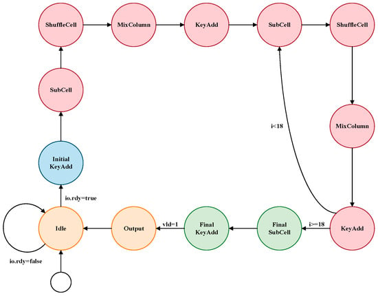
An FSM is a hardware sequential circuit comprising registers and combinational logic; it clarifies the hardware control logic by decomposing complex algorithmic processes into a series of clearly defined states [30,31]. This paper adopts a finite state machine approach for the top-level control of the Midori algorithm. Based on the logic of the Chisel source code, the FSM defines a total of nine states, with the state transitions shown in Figure 4.
Figure 4.
State transition diagram of Midori finite state machine.
Upon power-on reset, the state machine is initialized to the Idle state. When io.rdy is low, the state machine remains in the Idle state; as soon as io.rdy goes high, it immediately latches the input key and plaintext, resets the round counter i, and sets the valid output flag vld to low, then jumps to the Initial KeyAdd state to commence encryption, executing the AddRoundKey operation. After performing the XOR operation between the key and the initial plaintext, the system first executes an encryption round before proceeding to the main-loop iteration. The main loop consists of four states: SubCell, ShuffleCell, MixColumn and KeyAdd. After each state completes its corresponding combinational logic transformation, the state register is updated on the next clock edge and the system automatically jumps to the next functional state. The KeyAdd state serves as the loop control point, where the round counter i is evaluated. If the number of rounds is incomplete (i < 18), i is incremented by 1 and the process returns to SubCell for the next round; if 18 rounds have been completed (i ≥ 18), i is reset to zero, the loop is exited, and the system proceeds to the final-round processing. Final round processing first enters the Final SubCell state to execute the final SubCell substitution operation, then jumps to the Final KeyAdd state to execute the final AddRoundKey operation. Concurrently, the valid output flag vld is set to high, indicating that the ciphertext is valid, and the result is output. Finally, the state machine jumps to the Output state and automatically resets to the Idle state on the next clock cycle, awaiting the next encryption request.
3.2. Core Module Implementation
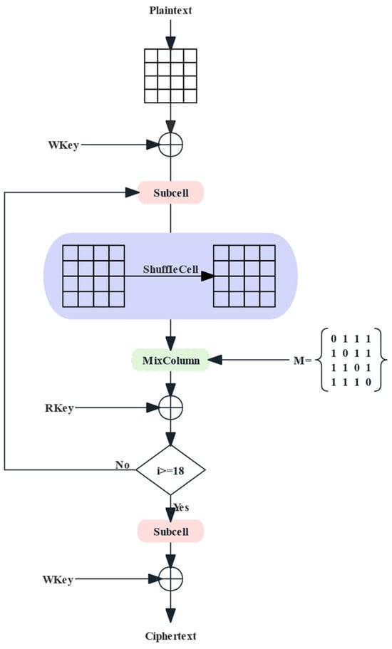
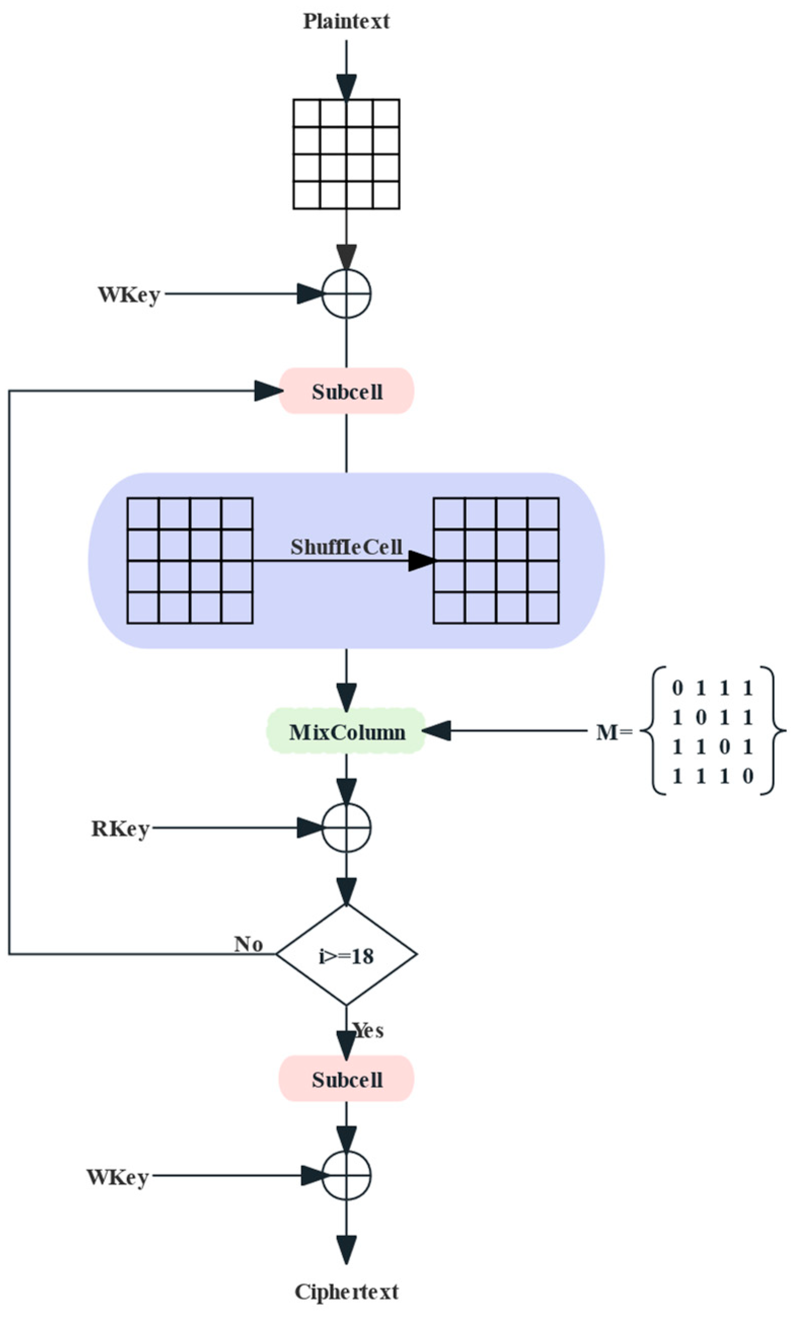
Figure 5 illustrates the ciphertext stream of the Midori-128 block cipher, the core of which is an SPN structure consisting of 18 rounds. The encryption process begins with an XOR operation between the plaintext and the White Key (WKey).
Figure 5.
Encryption routine of Midori-128.
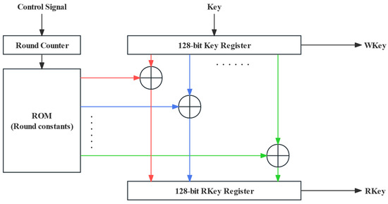
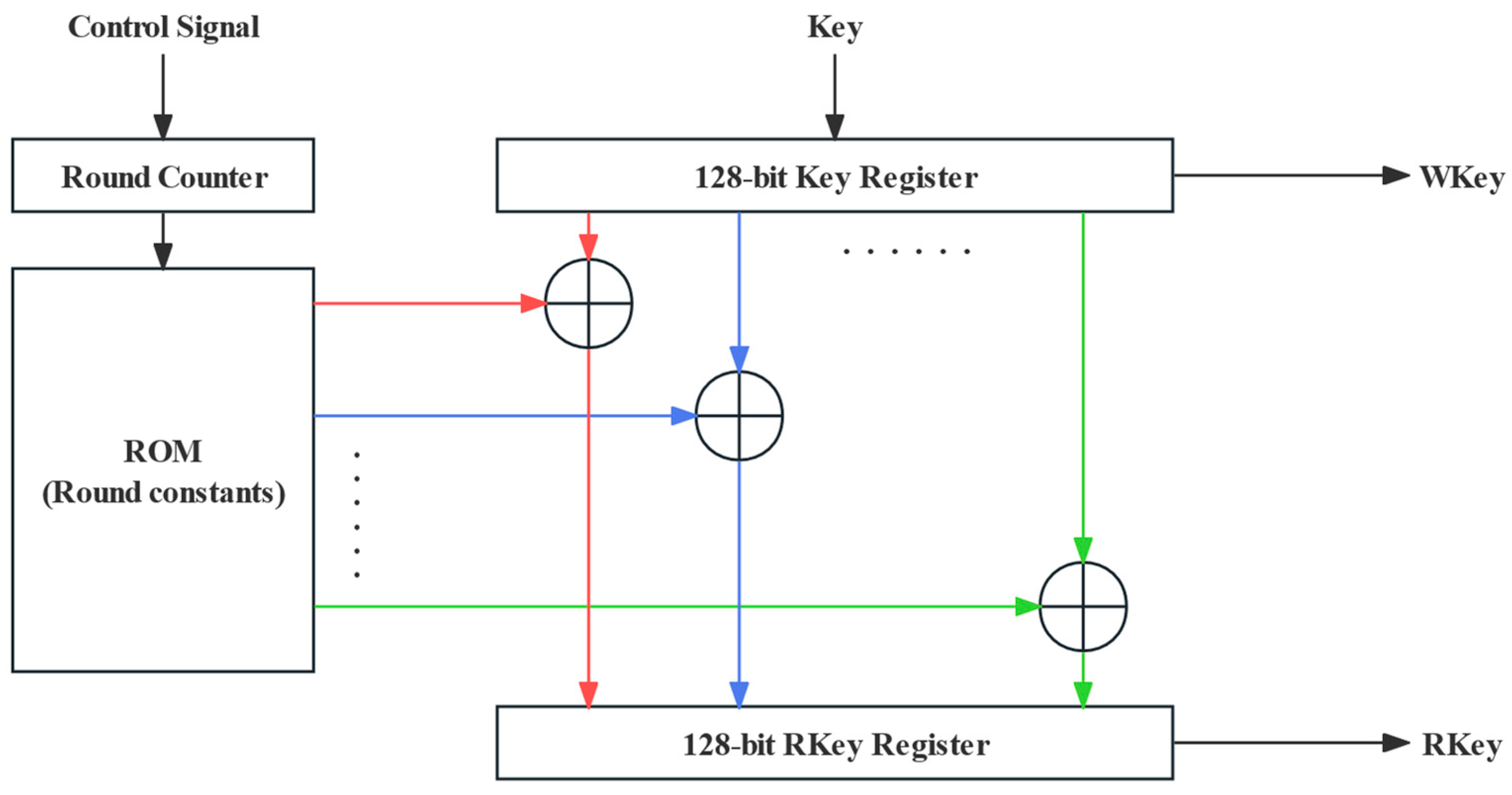
As can be seen from Figure 5, in each round, the ciphertext first undergoes a SubCell operation, using four different 4-bit S-boxes in parallel to perform non-linear substitution. Next, the ShuffleCell rearranges the 16 4-bit subcells in fixed positions to achieve diffusion between subcells. Then, the MixColumn transformation is applied, multiplying the four subcells in each column by a given binary matrix M to perform an XOR combination of the subcells within the column. Finally, the result is XORed with the round key (RKey) (see Figure 6 for the key generation process), completing one round of iteration. After iteration, the state undergoes another SubCell substitution and is ultimately XORed with WKey, producing a 128-bit ciphertext. This design ensures sufficient security while significantly reducing hardware implementation costs by simplifying the S-boxes and column mixing matrices, and omitting the final round of MixColumn operations. It fully embodies the optimization philosophy of Midori-128 as a lightweight block cipher.
Figure 6.
Key generation block diagram for Midori-128.
The round key generation module of Midori-128 employs a simple architecture, centered around a 128-bit master key register used to store the externally input key, which remains constant throughout the entire encryption process. In each round of operations, the control unit addresses the round constant ROM via the round counter, reads the corresponding 128-bit fixed constant βi for that round, and performs a bitwise XOR operation with the key to calculate the current round key RKey in real time. This is then stored in the round key register for use by the core unit’s AddKey operation. Simultaneously, the key is directly output as WKey for encrypting the initial plaintext. This design avoids complex key expansion iterations, relying solely on combinational logic and minimal storage resources to complete 20 rounds of key scheduling, thereby significantly reducing hardware power consumption and area.
3.3. Hardware Architecture
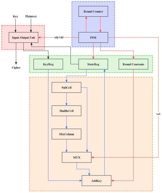
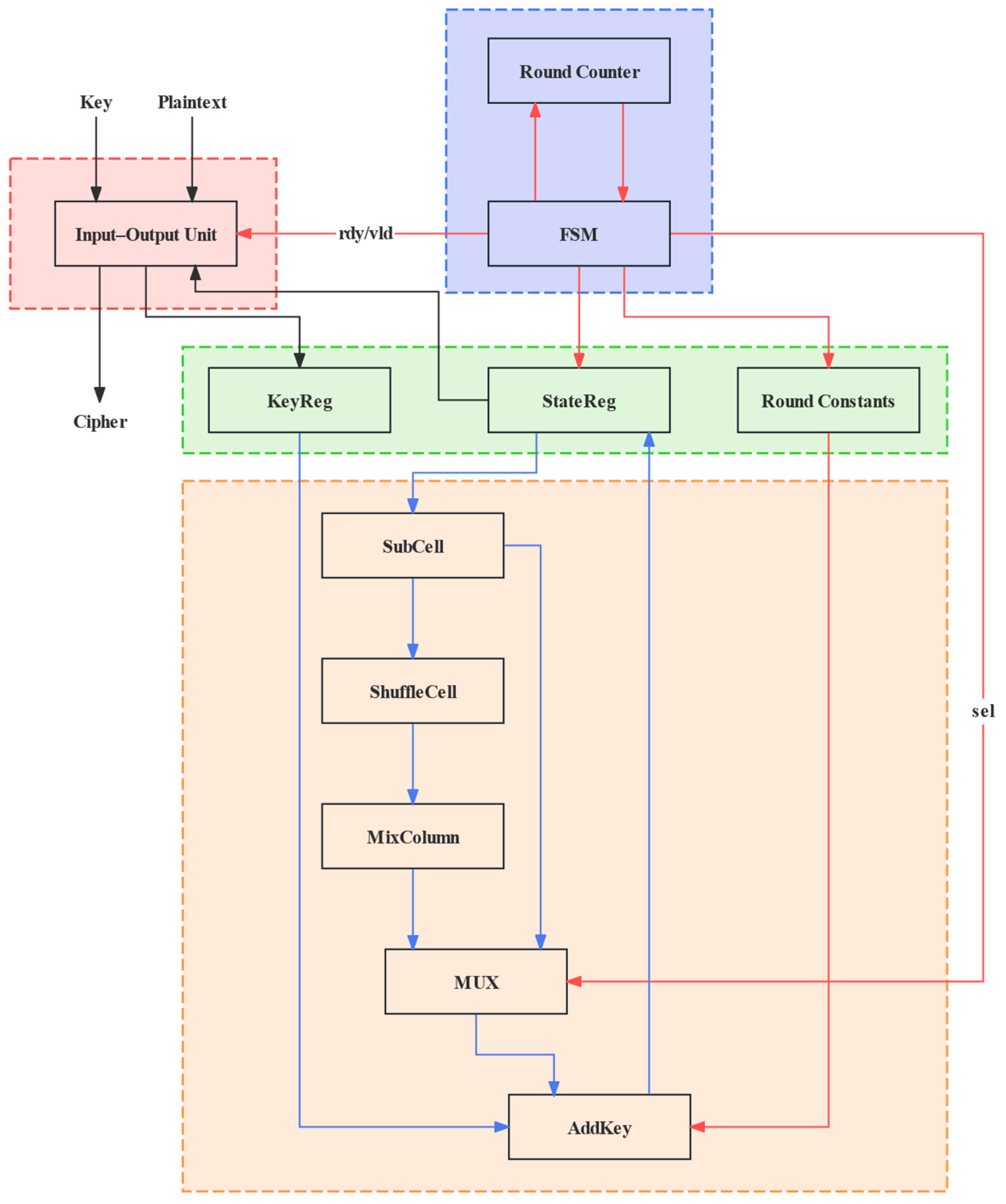
This paper proposes an area-optimized cyclic iterative structure; this design achieves higher throughput. The overall design follows a modular approach, comprising input–output units (red), control units (blue), storage units (green) and core arithmetic units (orange). Blue solid lines indicate the data path, while red lines indicate the control path. The hardware architecture is shown in Figure 7.
Figure 7.
Hardware architecture diagram.
The hardware architecture shown in Figure 7 forms the cryptographic core of the Midori-128 algorithm. The input–output unit receives the 128-bit key and plaintext via handshake signals, and ultimately outputs the ciphertext. The memory unit comprises the KeyReg, which stores the master key; the StateReg, which temporarily stores intermediate results; and a ROM that stores 20 round constants. The core computational unit consists of SubCell, ShuffleCell, MixColumn and AddKey, with the final round bypass implemented via a MUX. The control unit comprises an FSM and a round counter, responsible for generating all control signals. During operation, the plaintext is white-boxed with the master key and stored in StateReg. Subsequently, in each round, the round key is synthesized in real time from KeyReg and the round constant to participate in the AddKey operation.
The final-round multiplexer bypass, which skips the MixColumn operation, is controlled by a registered FSM synchronized with the round counter. In the final round, the registered select signal ‘sel’ directly forwards the ShuffleCell output to the AddKey stage, eliminating any combinational feedback loops by ensuring all control signals are clock-synchronized and the only feedback path passes through the registered StateReg.
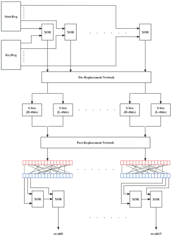
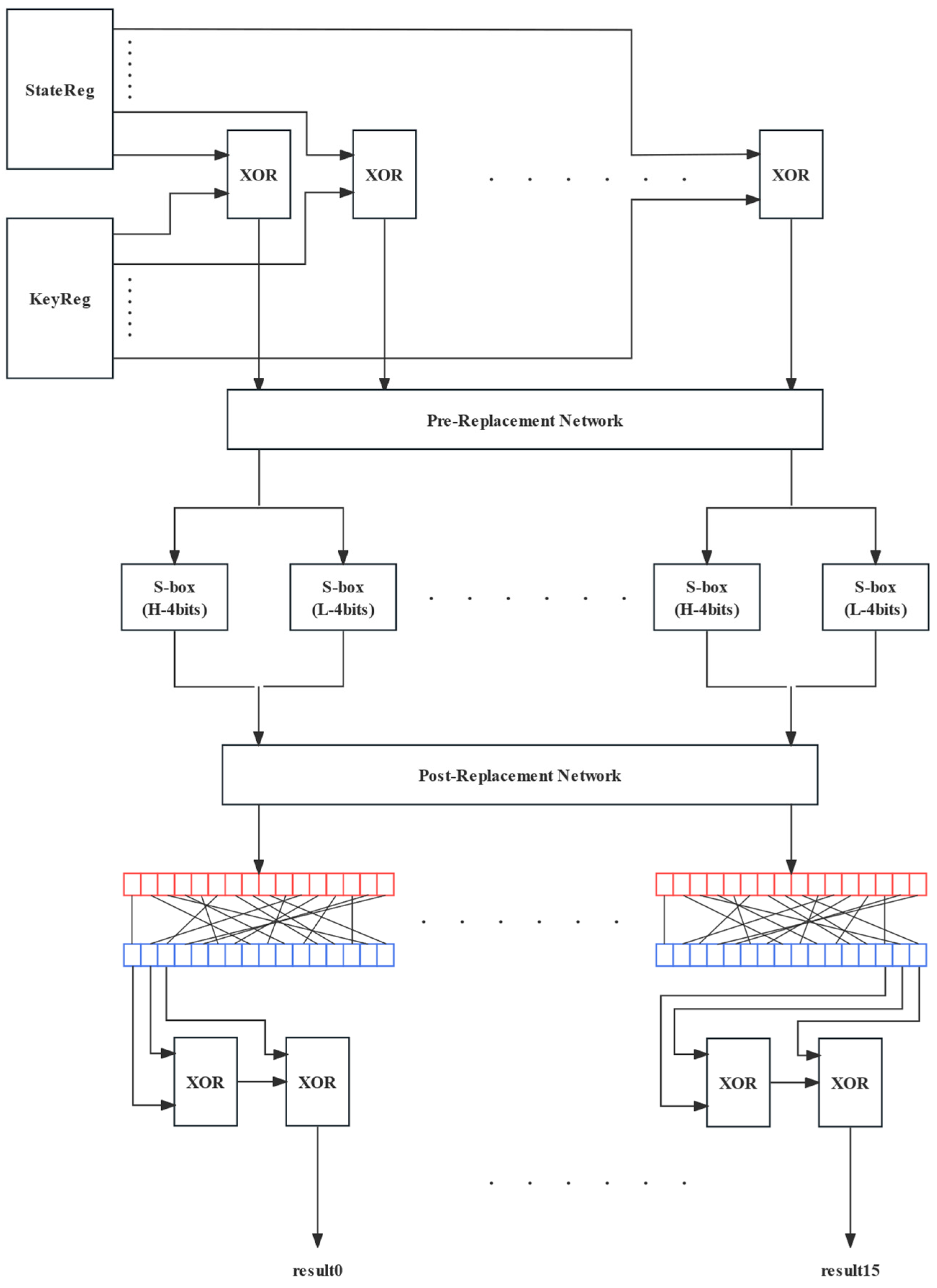
The round function operations and round key operations form the core of this architecture. The structure of the round key operation section is shown in Figure 6, whilst the detailed hardware structure of the round function section is illustrated in Figure 8.
Figure 8.
Hardware structure diagram of the round function.
Figure 8 illustrates the complete hardware data path of the Midori-128 algorithm’s round function. The 128-bit state data in the state register is first XORed with the round key provided by the key register. The result of the XOR operation enters the pre-processing network, where each 8-bit byte is split into upper and lower 4-bit halves, which are fed into the H-4bits S-box and L-4bits S-box, respectively, for non-linear permutation, before being recombined via the post-processing network to restore the 8-bit output. Subsequently, the data stream directly implements ShuffleCell byte permutation and MixColumn column mixing at the hardware interconnect level; the former alters byte positions via the routing network, whilst the latter performs matrix multiplication for each column via combinational logic. The final result is output as 16 bytes (result0–result15), which are written back to the state register as input for the next round. Table 4 illustrates the detailed evolution of the data stream within each clock cycle during a single round of the Midori-128 encryption operation. The table lists, cycle by cycle, the step-by-step updates to the Internal State as it passes through the four operational steps: SubCell, ShuffleCell, MixColumn, and AddRoundKey.
Table 4.
Data flow in every cycle for one round.
4. Testing and Performance Analysis
This design has been successfully implemented on five FPGA platforms. The low cost of FPGA development makes it the preferred option for hardware implementation [32]. This section presents a comparative analysis of cryptographic algorithms from the existing literature, with the results summarized in tabular form. To verify the functional correctness of the proposed design and evaluate its hardware performance, this study first performed functional simulation of the design using the ChiselTest framework built into the Chisel language, followed by timing analysis within the IntelliJ IDEA software environment. Finally, a comprehensive analysis was conducted using Pango Design Suite 2022.2-SP6.4 (sourced from Pango Microsystems Inc., Shenzhen, China), Vivado 2018.3 and Xilinx ISE Design Suite 14.7 (both sourced from Xilinx Inc., San Jose, CA, USA). For the domestic PGL100H platform, we used Pango Design Suite 2022.2-SP6.4 targeting the PGL100H-5FBG900 device with a clock constraint of the maximum achievable frequency. For other platforms, similar default constraints were applied.
To account for the variability introduced by initial seeds in the implementation process, we performed multiple synthesis and place-and-route runs for each platform with different initial seed values (e.g., 1, 3, and 5). The reported area, frequency, and power results are the averages across these runs, and the corresponding standard deviations are provided as error bars in the relevant figures. This section also provides a power consumption and energy consumption analysis of the design; the power consumption analysis utilized the XPower Analyzer and Power Calculator tools.
4.1. Midori Simulation Testing
To verify the functional correctness of this design, this section performs functional simulation verification of the Midori encryption module using Chisel’s built-in ChiselTest framework, with visual verification carried out using the GTKWave waveform analysis tool. The official standard test vectors are shown in Table 5.
Table 5.
Midori-128 Test Vectors.
The following test uses test vector 1 as an example. The simulation results demonstrate that the encryption module designed in this paper is capable of correctly converting standard plaintext into the expected ciphertext, thereby verifying the logical correctness of the proposed hardware design, and this work focuses on hardware implementation and performance evaluation.
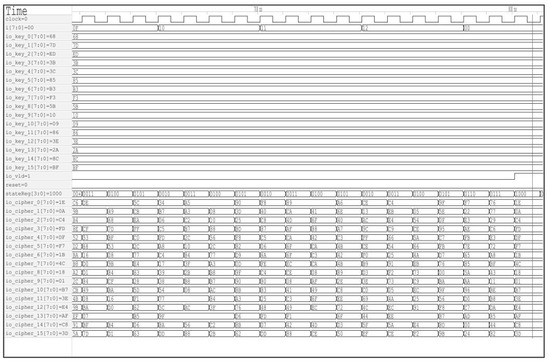
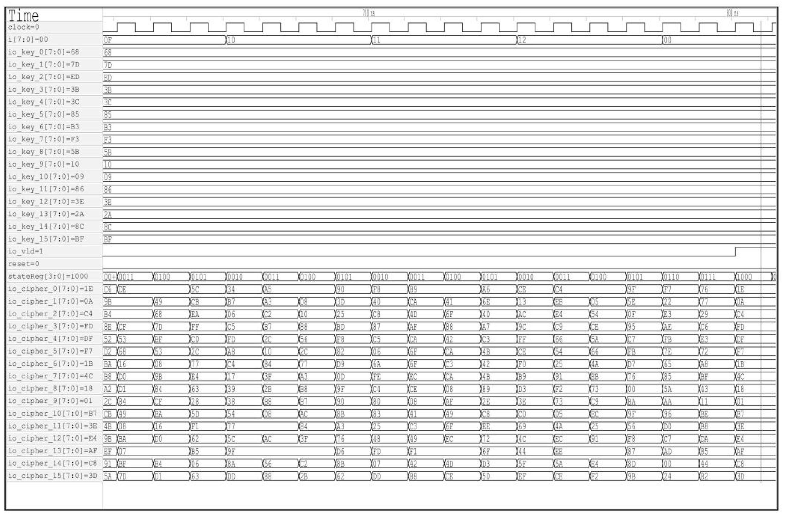
The functional simulation waveform of the module is shown in Figure 9. As can be seen from Figure 9, the value of the output enable signal io_vld is 1, indicating that the output is enabled; at this point, the final value of the output io_cipher is 1e0ac4fddff71b4c1801b73ee4afc83d. At the same time, the value of stateReg is 1000, indicating that the entire process has been completed and has entered the result state.
Figure 9.
Test waveform diagram.
This simulation verification was carried out entirely using Chisel’s built-in ChiselTest framework. Compared to the complex process involved in traditional FPGA development—which requires writing testbenches in Verilog and relying on third-party EDA tools such as ModelSim and VCS for co-simulation—ChiselTest allows designers to write test code directly within the Scala environment, applying a software development approach to instantiate hardware modules, apply stimuli and assert results. This software-based verification approach not only greatly simplifies the construction of the test environment but also significantly improves the efficiency of hardware design iteration and debugging, fully demonstrating Chisel’s advantages in agile hardware development convenience.
4.2. Results from the FPGA Platform
To ensure greater accuracy, the results were obtained following a comprehensive analysis. Furthermore, to enable a fair comparison with other cryptographic algorithms, all performance metrics were quantified for implementations across different FPGA families, including Virtex-5(xc5vlx330-2ff1760), Virtex-7(xc7v585tffg1157-3), Artix-7(xc7a200tfbg676-3), Spartan-6(xc6slx150tfgg676-2) and PGL100H(5FBG900). Table 6 presents resource utilization, data throughput and power consumption figures for the Artix-7 platform, alongside standardized performance metrics such as power consumption per bit and energy efficiency.
Table 6.
Hardware performance metrics for FPGA implementation of MIDORI algorithm in Artix-7.
When discussing the performance of the Midori algorithm, its throughput is a key metric for measuring processing efficiency [33], and is calculated as follows:
where BlockSize represents the data block size for each processing unit; in this context, it refers to the block length of the Midori encryption algorithm, which is 128 bits. Frequency represents the system clock frequency, which is determined by the synthesis tool through critical path delay analysis. CyclesPerBlock denotes the number of clock cycles required to process a single data block. This design employs a non-pipeline multi-cycle architecture. The clock cycles required for a single encryption cycle can be determined through analysis of the state transition diagram shown in Figure 4. The entire iterative process concludes when the cyclic counter i reaches 18, with each iteration requiring 4 clock cycles. Adding the S-box substitution and round key addition operations performed before and after the iteration, the total number of clock cycles required for the entire module is 78. During this period, the data path cannot receive new plaintext inputs and must wait for the current block output valid signal to be set before initiating the next block loading.
Throughput per area represents the core metric for evaluating hardware design efficiency, with the following calculation formula:
Energy consumption is a key metric for assessing the energy efficiency of hardware implementations of cryptographic algorithms [34,35], and is calculated as follows:
where Ptotal represents the total power consumed by the chip under normal operating conditions, whilst T represents the time required to complete one full encryption cycle.
Energy per area serves as the key metric for evaluating hardware design energy efficiency, with the following calculation formula:
Furthermore, efficiency is typically calculated as throughput per unit area; this is a standardized parameter that allows for a fair comparison with other lightweight ciphers [36,37], and is calculated as follows:
The formula for calculating the critical path delay is
where Tclk represents the clock period and WNS represents the worst-case negative margin. Fmax can be calculated from the critical path delay data using the following formula:
However, in engineering practice, a timing margin of 0.2 ns to 0.3 ns is typically required to account for fluctuations in process conditions, voltage and temperature; therefore, the formula for the maximum stable operating frequency that can be achieved in practice is
4.3. Analysis of Results
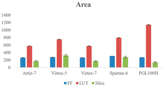
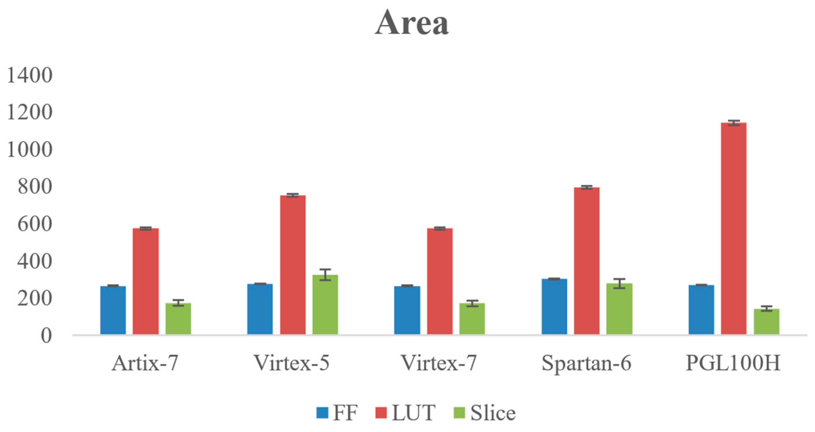
The resource utilization of different FPGA series is shown in Figure 10. As can be seen from Figure 10, the Virtex-7 is the optimal choice for applications requiring low-cost, low-power FPGA sensor nodes and devices. Conversely, for projects involving complex control logic, the PGL100H offers significant advantages. Although it utilizes the highest amount of LUT resources among the devices, it can complete logic mapping with the least amount of slice resources. Both its logic density and slice utilization are superior to those of other devices, enabling the implementation of complex functions with a smaller area footprint.
Figure 10.
Graph showing area utilization of Midori-128.
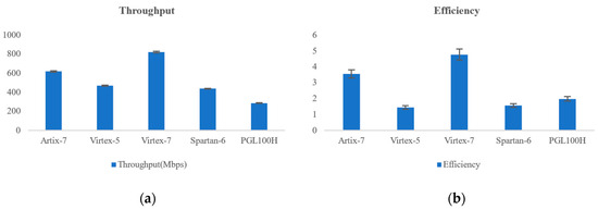
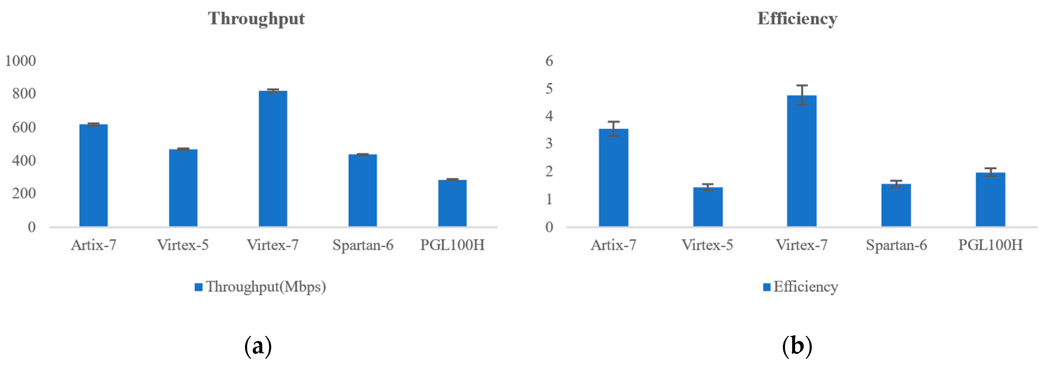
Figure 11 illustrates the data throughput and efficiency of different FPGA platforms. The data shows that the Artix-7 and Virtex-7 achieve a better balance between throughput and efficiency: the Virtex-7 achieves a throughput of 820.51 Mbps at maximum efficiency, whilst the Artix-7 maintains a high efficiency of 3.56 at a throughput of 619.26 Mbps. In contrast, other platforms such as the Virtex-5, whilst offering high throughput, exhibit lower efficiency.
Figure 11.
Graph showing throughput and efficiency of Midori-128: (a) Throughput of Midori-128; (b) efficiency of Midori-128.
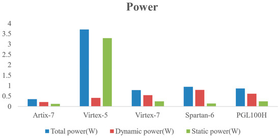
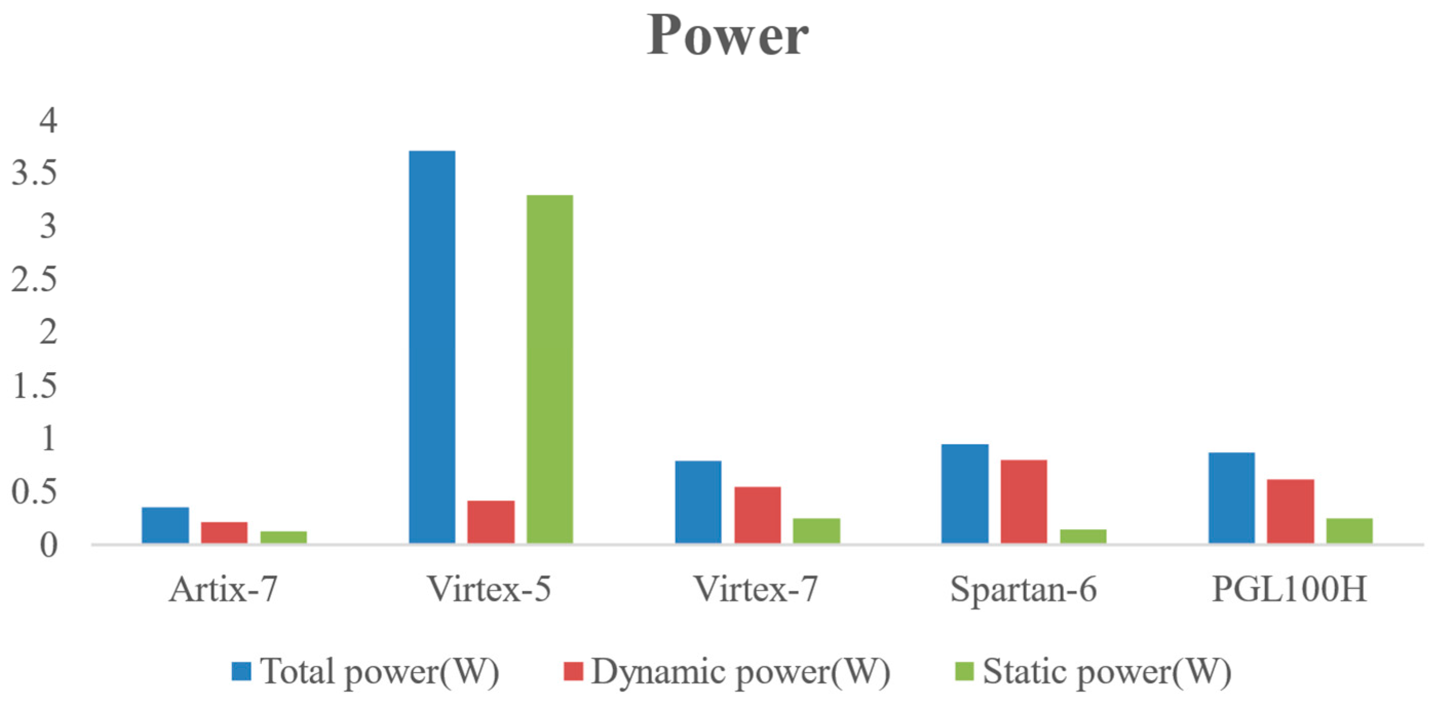
Furthermore, in terms of power consumption, there are significant differences between various FPGA platforms, as shown in Figure 12. The Artix-7 has the lowest total power consumption, making it the ideal choice for low-power applications. The Virtex-7 and Spartan-6 also perform exceptionally well, with total power consumption of 0.79 W and 0.95 W respectively. In contrast, the Virtex-5 has a total power consumption as high as 3.71 W, almost entirely attributable to static power consumption, making it unsuitable for power-sensitive applications. The high total power of 3.71 W on the Virtex-5 platform is dominated by static leakage power, an inherent characteristic of the 65 nm bulk CMOS process and global FPGA architecture, rather than a design or constraint issue. As documented in Xilinx’s official datasheet, Virtex-5 devices exhibit large subthreshold leakage currents even at room temperature, which cannot be fully eliminated by EDA tools. The quiescent core current of mid-to-large LX devices exceeds 650 mA at nominal voltage, leading to typical static power well above 3 W for lightly utilized configurations. Our measured dynamic power of only 0.417 W confirms that the design itself is efficient; the remaining 3.294 W is consistent with the official static power envelope of the Virtex-5 family.
Figure 12.
Graph showing power of Midori-128.
Therefore, if low power consumption is the primary design objective, the Artix-7 is the optimal choice; if a certain level of performance is also required, the Virtex-7 or Artix-7 can provide a good balance at relatively low power consumption.
4.4. Comparative Discussion
This section presents a multi-dimensional comparison of the Midori-128 hardware implementation proposed in this paper with relevant published work. It validates the advantages of the design in terms of resource utilization, operating frequency, throughput, power consumption and efficiency. The comparative data are derived from the publicly available literature and the experimental results of this study, covering mainstream FPGA platforms such as Spartan-6, Artix-7, Virtex-5, Virtex-7 and the domestically produced PGL100H. The data is presented in Table 7. In terms of frequency performance, the implementation based on the Spartan-6 platform achieves an operating frequency of 266.8 MHz, representing an increase of approximately 91.51% compared to the 139.31 MHz achieved by the Serial-1 architecture in Reference [13], an increase of approximately 209.98% compared to the 86.07 MHz achieved by the Serial-2 architecture in Reference [13], and an increase of approximately 108.58% compared to the 127.91 MHz reported in Reference [10], thereby unlocking greater performance potential in low-cost FPGAs.
Table 7.
Performance comparisons of the lightweight block cipher implemented in FPGA platform.
In terms of throughput and power consumption, the design presented in this paper demonstrates significant advantages in both performance and energy efficiency. On the Virtex-5 platform, the throughput achieved in this paper reached 470.88 Mbps, representing an improvement of approximately 42.5% over the results reported in Reference [10]. On the Spartan-6 platform, the throughput achieved in this study reached 437.83 Mbps, representing an increase of approximately 124.63% compared to Reference [10]; although resource consumption has increased, the improvement in throughput is more significant. A trade-off analysis reveals that the throughput improvement is achieved with a moderate increase in area, making the design suitable for performance-oriented IoT edge devices.
On the domestically developed PGL100H platform, the throughput achieved in this study reached 287.19 Mbps, with an efficiency of 1.99. This is significantly higher than the efficiency achieved by the serial architecture described in Reference [13] when implemented on the Xilinx Spartan-6 platform, demonstrating the feasibility and performance of the design proposed in this study on a domestically developed and controllable FPGA platform.
From the perspectives of overall efficiency and application coverage, the design presented in this paper offers a distinct competitive advantage. It supports five categories of FPGA platforms, including low-cost (Spartan-6), high-performance (Artix-7, Virtex-5, Virtex-7) and domestically developed (PGL100H) options, thereby meeting diverse requirements ranging from consumer electronics to high-end communications, and from commercial platforms to scenarios requiring independent control. With high performance, low power consumption and multi-platform adaptability as its core features, the design possesses irreplaceable application value in high-end encryption acceleration and edge computing scenarios.
Overall, the Midori-128 hardware implementation proposed in this paper demonstrates significant advantages in peak performance, energy efficiency and cross-platform adaptability. It achieves the highest operating frequency and throughput across all tables on the Virtex-7 platform, whilst maintaining extremely low power consumption at high throughput levels. Furthermore, it operates stably on domestic FPGA, providing a more competitive solution for the hardware deployment of lightweight block ciphers across various scenarios.
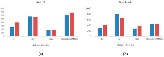
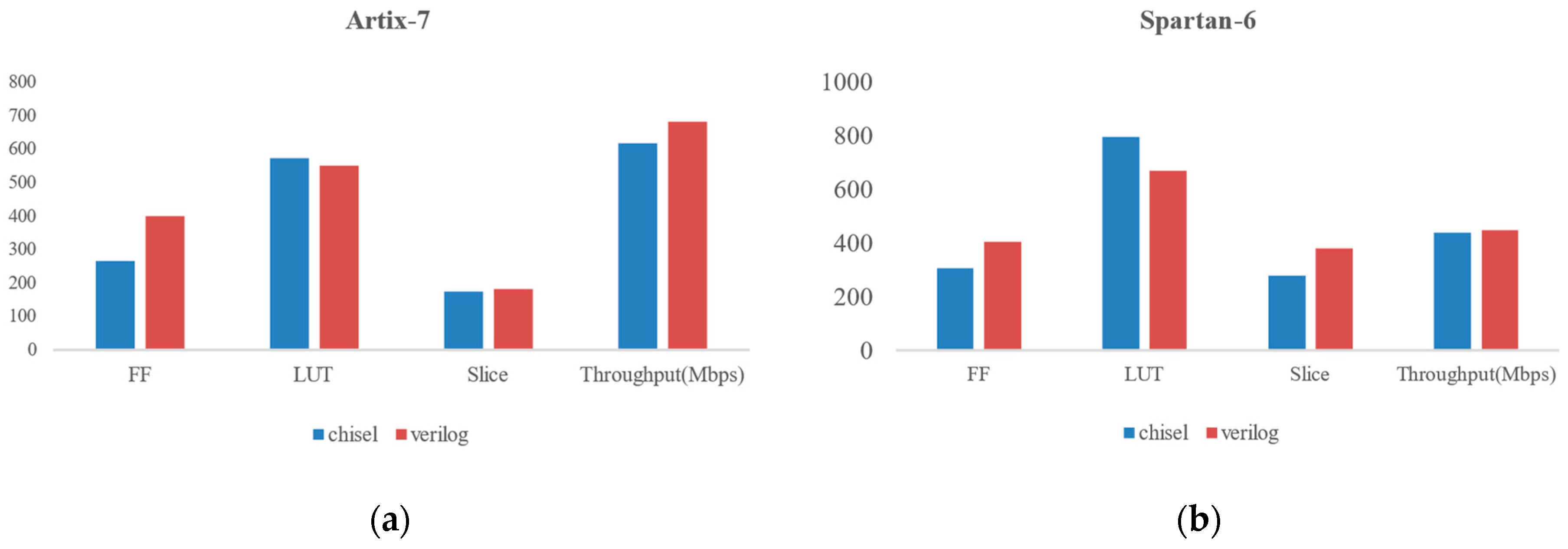
Furthermore, while maintaining identical functionalities, this design compares the area and throughput of Verilog versus Chisel implementations across Artix-7 and Spartan-6 platforms, with results presented in Table 8.
Table 8.
Comparison of resource utilization and throughput.
To provide a more visual comparison of the two sets of data, a chart has been produced, as shown in Figure 13.
Figure 13.
Comparison of resource utilization and throughput between Chisel and Verilog implementations: (a) Artix-7; (b) Spartan-6.
5. Conclusions
This paper addresses the low efficiency and long development cycles of traditional Verilog HDL in cryptographic algorithm implementation. By leveraging the high-level abstraction and modular design capabilities of the Chisel language, we propose a hardware implementation of the Midori-128 lightweight block cipher. Experimental results on multiple FPGA platforms show that the proposed design achieves significant throughput gains compared to prior Verilog-based works. Specifically, on the Spartan-6 platform, our design reaches a throughput of 437.83 Mbps, an increase of approximately 124.63% over the reference implementation [10]; on Virtex-5, the throughput improves by about 42.5% to 470.88 Mbps.
Furthermore, the parametric and reusable nature of Chisel enables rapid adaptation to different FPGA families. The best throughput of 820.51 Mbps is achieved on Virtex-7 with an efficiency of 4.77 Mbps/LUT. These results confirm that adopting Chisel not only accelerates hardware development but also delivers measurable performance benefits for lightweight block cipher implementations, providing a competitive solution for resource-constrained IoT and edge security applications.
Author Contributions
Conceptualization, J.W.; Methodology, J.W. and H.X.; Software, H.X.; Validation, J.W., H.X. and D.D.; Formal analysis, J.W.; Resources, C.X.; Data curation, C.X. and L.Z.; Writing—original draft, J.W. and H.X.; Writing—review and editing, J.W. and H.X.; Supervision, C.X., L.Z. and D.D.; Project administration, C.X., L.Z. and D.D.; Funding acquisition, J.W. All authors have read and agreed to the published version of the manuscript.
Funding
This research was funded by the Central Universities Basic Scientific Research Fund, grant number 3282025047.
Data Availability Statement
The original contributions presented in this study are included in the article. Further inquiries can be directed to the corresponding author.
Acknowledgments
We acknowledge the administrative and technical support provided by our institution.
Conflicts of Interest
The authors declare that they have no known competing financial interests or personal relationships that could have appeared to influence the work reported in this paper.
References
- Tan, C.C. A Mini Review on Edge Computing Devices for IoT Systems. Emerg. Adv. Integr. Technol. 2025, 6, 64–80. [Google Scholar] [CrossRef] [Scilit]
- Altaibek, M.; Issainova, A.; Aidynov, T.; Kuttymbek, D.; Abisheva, G.; Nurusheva, A. A Survey of Cross-Layer Security for Resource-Constrained IoT Devices. Appl. Sci. 2025, 15, 9691. [Google Scholar] [CrossRef] [Scilit]
- Kushwaha, J.P.; Bhadauria, S.; Tapaswi, S. Unveiling IoT ecosystem security: A review of intelligent IDS, trends, challenges, and future directions. Comput. Electr. Eng. 2025, 128, 110626. [Google Scholar] [CrossRef] [Scilit]
- Kia, A.; Storey, A.W.; Imtiaz, M. Advanced Hardware Security on Embedded Processors: A 2026 Systematic Review. Electronics 2026, 15, 1135. [Google Scholar] [CrossRef] [Scilit]
- Ahmed, S.; Ahmad, N.; Shah, N.A.; Abro, G.E.M.; Wijayanto, A.; Hirsi, A.; Altaf, A.R. Lightweight AES Design for IoT Applications: Optimizations in FPGA and ASIC With DFA Countermeasure Strategies. IEEE Access 2025, 13, 22489–22509. [Google Scholar] [CrossRef] [Scilit]
- Bi, H.; Wang, P.; Ye, J.; Zhao, L.; Zhang, Y.; Chen, B. A RRAM-based logic in memory DES implementation against power attacks. Microelectron. Eng. 2025, 299, 112356. [Google Scholar] [CrossRef] [Scilit]
- Thakor, V.A.; Razzaque, M.A.; Khandaker, M.R.A. Lightweight Cryptography Algorithms for Resource-Constrained IoT Devices: A Review, Comparison and Research Opportunities. IEEE Access 2021, 9, 28177–28193. [Google Scholar] [CrossRef] [Scilit]
- Elminaam, D.S.A.; Kader, H.M.A.; Hadhoud, M.M. Trade offs between Energy Consumption and Security of Symmetric Encryption Algorithms. Int. J. Comput. Theory Eng. 2009, 1, 325–333. [Google Scholar] [CrossRef] [Scilit]
- Al-Nofaie, S.M.; Sharaf, S.; Molla, R. Design Trends and Comparative Analysis of Lightweight Block Ciphers for IoTs. Appl. Sci. 2025, 15, 7740. [Google Scholar] [CrossRef] [Scilit]
- Kella, C.; Singh, P.; Mishra, Z.; Acharya, B. Area-efficient architectures of Midori lightweight block cipher for resource constrained devices. Integration 2025, 105, 102501. [Google Scholar] [CrossRef] [Scilit]
- Baghel, A.; Mishra, Z.; Parmar, O.; Rajput, A.S. Optimised architectures of Midori block cipher for area-constrained IoT applications. Int. J. High Perform. Syst. Archit. 2023, 11, 206–215. [Google Scholar] [CrossRef] [Scilit]
- Banik, S.; Bogdanov, A.; Isobe, T.; Shibutani, K.; Hiwatari, H.; Akishita, T.; Regazzoni, F. Midori: A Block Cipher for Low Energy. In Advances in Cryptology—ASIACRYPT 2015; Part II: LNCS 9453; Springer: Berlin/Heidelberg, Germany, 2015; pp. 411–436. [Google Scholar] [CrossRef] [Scilit]
- Lara-Nino, C.A.; Diaz-Perez, A.; Morales-Sandoval, M. FPGA-Based Assessment of Midori and GIFT Lightweight Block Ciphers. In Information and Communications Security; ICICS 2018, LNCS 11149; Springer: Cham, Switzerland, 2018; pp. 745–755. [Google Scholar] [CrossRef] [Scilit]
- An, C.; Bai, W.; Zhang, D. Meet-in-the-middle differential fault analysis on Midori. Electron. Res. Arch. 2023, 31, 6820–6832. [Google Scholar] [CrossRef] [Scilit]
- Rezaei Shahmirzadi, A.; Azimi, S.A.; Salmasizadeh, M.; Mohajeri, J.; Aref, M.R. Impossible differential cryptanalysis of reduced-round Midori64 block cipher (extended version). ISC Int. J. Inf. Secur. 2018, 10, 3–13. [Google Scholar] [CrossRef] [Scilit]
- Liu, J.; Li, M.; Ren, J.; Chen, S. A Highly Efficient Neural Distinguisher Framework for IoT-Friendly Lightweight SPN Block Ciphers. IEICE Trans. Inf. Syst. 2026, E109-D, 238–248. [Google Scholar] [CrossRef] [Scilit]
- Mishra, R.; Okade, M.; Mahapatra, K. Efficient hardware mapping of Boolean substitution boxes based on functional decomposition for RFID and ISM band IoT applications. Integration 2023, 92, 38–47. [Google Scholar] [CrossRef] [Scilit]
- Bachrach, J.; Vo, H.; Richards, B.; Lee, Y.; Waterman, A.; Avižienis, R.; Wawrzynek, J.; Asanović, K. Chisel: Constructing Hardware in a Scala Embedded Language. In DAC ’12: Proceedings of the 49th Annual Design Automation Conference; Association for Computing Machinery: New York, NY, USA, 2012; pp. 1216–1225. [Google Scholar] [CrossRef] [Scilit]
- Dobis, A.; Laeufer, K.; Damsgaard, H.J.; Petersen, T.; Rasmussen, K.J.H.; Tolotto, E.; Andersen, S.T.; Lin, R.; Schoeberl, M. Verification of Chisel Hardware Designs with ChiselVerify. Microprocess. Microsyst. 2022, 94, 104636. [Google Scholar] [CrossRef] [Scilit]
- Schoeberl, M.; Damsgaard, H.J.; Pezzarossa, L.; Keszocze, O.; Jellum, E.R.; Beamer, S. Scala Defined Hardware Generators for Chisel. Microprocess. Microsyst. 2025, 117, 105182. [Google Scholar] [CrossRef] [Scilit]
- Liew, H.; Sheikh, F.; Guo, J.-R.; Wu, Z.; Nikolić, B. A Chisel Generator for Standardized 3-D Die-to-Die Interconnects. IEEE J. Explor. Solid-State Comput. Devices Circuits 2024, 10, 58–66. [Google Scholar] [CrossRef] [Scilit]
- Bruant, J.; Horrein, P.H.; Muller, O.; Groleat, T.; Pétrot, F. Toward agile hardware designs with Chisel: A network use case. IEEE Des. Test 2021, 39, 77–84. [Google Scholar] [CrossRef] [Scilit]
- Feng, J.Y.; Li, L.; Guo, Y.; Huang, X.T. Research on FPGA optimization of Midori cipher algorithm. J. Hengyang Norm. Univ. 2020, 41, 44–48. [Google Scholar] [CrossRef]
- Ru, H.J. A new kind linear analysis of invariant bias of midori-64 related keys. In Artificial Intelligence and Security; Communications in Computer and Information Science, 1254 CCIS; Springer: Singapore, 2020; pp. 376–384. [Google Scholar] [CrossRef] [Scilit]
- Liu, W.; Yang, Y. The 7-Round Subspace Trail-Based Impossible Differential Distinguisher of Midori-64. Secur. Commun. Netw. 2021, 2021, 6269604. [Google Scholar] [CrossRef] [Scilit]
- Zhao, H.; Han, G.; Xing, Z. Related-Key Differential Cryptanalysis of Midori-64 Based on Invariant Subspace. KSII Trans. Internet Inf. Syst. 2024, 18, 3293–3305. [Google Scholar] [CrossRef] [Scilit]
- Shen, S.; Liu, Y.; Zhang, L.; Song, F.; Wu, Z. Formal verification of RISC-V processor Chisel designs. In Dependable Software Engineering. Theories, Tools, and Applications: 10th International Symposium, SETTA 2024; Springer: Singapore, 2025; pp. 142–160. [Google Scholar] [CrossRef] [Scilit]
- Käyrä, M.; Hämäläinen, T.D. A Survey on System-on-a-Chip Design Using Chisel HW Construction Language. In IECON 2021-47th Annual Conference of the IEEE Industrial Electronics Society; IEEE: Piscataway Township, NJ, USA, 2021; pp. 1–6. [Google Scholar] [CrossRef] [Scilit]
- Ferres, B.; Muller, O.; Rousseau, F. A Chisel Framework for Flexible Design Space Exploration through a Functional Approach. ACM Trans. Des. Autom. Electron. Syst. 2023, 28, 1–31. [Google Scholar] [CrossRef] [Scilit]
- Barkalov, A.; Titarenko, L.; Krzywicki, K. Improving Characteristics of LUT-Based Sequential Blocks for Cyber-Physical Systems. Energies 2022, 15, 2636. [Google Scholar] [CrossRef] [Scilit]
- Salauyou, V. Technique for Constructing Structural Models of Fault-Tolerant Moore Finite State Machines. In Advances in Dependable Systems and Networks, Proceedings of the 20th International Conference on Dependability of Computer Systems (DEPCOS-RELCOMEX 2025); Lecture Notes in Networks and Systems; Springer: Cham, Switzerland, 2025; Volume 1427. [Google Scholar] [CrossRef] [Scilit]
- Guru Siva Subramanian, V.; Deepika Sree, T.N.; Aditya, S. A Low cost area-efficient modified Russian peasant multiplier (MRPM) for biomedical applications. Integration 2025, 104, 102474. [Google Scholar] [CrossRef] [Scilit]
- Hatzivasilis, G.; Fysarakis, K.; Papaefstathiou, I.; Manifavas, C. A review of lightweight block ciphers. J. Cryptogr. Eng. 2018, 8, 141–184. [Google Scholar] [CrossRef] [Scilit]
- Rana, M.; Mamun, Q.; Islam, R. Balancing Security and Efficiency: A Power Consumption Analysis of a Lightweight Block Cipher. Electronics 2024, 13, 4325. [Google Scholar] [CrossRef] [Scilit]
- Schmid, M.; Arul, T.; Kavun, E.B.; Regazzoni, F.; Kara, O. Robust and Energy-Efficient Hardware Architectures for Dizy Stream Cipher. In IEEE Asia Pacific Conference on Circuits and Systems (APCCAS); IEEE: Piscataway Township, NJ, USA, 2024; pp. 461–465. [Google Scholar] [CrossRef] [Scilit]
- Naik, M.S.; Sreekantha, D.K.; Sairam, K.V.S.S.S. Comparative study of block ciphers implementation for resource-constrained devices (Review). Radioelectron. Commun. Syst. 2024, 66, 123–137. [Google Scholar] [CrossRef] [Scilit]
- Ueno, R.; Morioka, S.; Homma, N.; Aoki, T. High Throughput/Gate AES Hardware Architectures Based on Datapath Compression. IEEE Trans. Comput. 2020, 69, 534–548. [Google Scholar] [CrossRef] [Scilit]





Disclaimer/Publisher’s Note: The statements, opinions and data contained in all publications are solely those of the individual author(s) and contributor(s) and not of MDPI and/or the editor(s). MDPI and/or the editor(s) disclaim responsibility for any injury to people or property resulting from any ideas, methods, instructions or products referred to in the content. |
© 2026 by the authors. Licensee MDPI, Basel, Switzerland. This article is an open access article distributed under the terms and conditions of the Creative Commons Attribution (CC BY) license.