


Abstract
Industrial-grade printed circuit boards (PCBs) exhibit high structural order and inherent geometric symmetry, where minute surface defects essentially constitute symmetry-breaking anomalies that disrupt topological integrity. Detecting these anomalies is quite challenging due to issues like scale variation and low contrast. Therefore, this paper proposes a symmetry-aware object detection framework, DAS-YOLO, based on an improved YOLOv11. The U-shaped adaptive feature extraction module (Def-UAD) reconstructs the C3K2 unit, overcoming the geometric limitations of standard convolutions through a deformation adaptation mechanism. This significantly enhances feature extraction capabilities for irregular defect topologies. A semantic-aware module (SADRM) is introduced at the backbone and neck regions. The lightweight and efficient ESSAttn improves the distinguishability of small or weak targets. At the same time, to address information asymmetry between deep and shallow features, an iterative attention feature fusion module (IAFF) is designed. By dynamically weighting and calibrating feature biases, it achieves structured coordination and balanced multi-scale representation. To evaluate the validity of the proposed method, we carried out comprehensive experiments using publicly accessible datasets focused on PCB defects. The results show that the Recall, mAP@50, and mAP@50-95 of DAS-YOLO reached 82.60%, 89.50%, and 46.60%, respectively, which are 3.7%, 1.8%, and 2.9% higher than those of the baseline model, YOLOv11n. Comparisons with mainstream detectors such as GD-YOLO and SRN further demonstrate a significant advantage in detection accuracy. These results confirm that the proposed framework offers a solution that strikes a balance between accuracy and practicality in addressing the key challenges in PCB surface defect detection.
1. Introduction
Over the past few years, fueled by digital transformation and the accelerated rollout of cutting-edge technologies including 5G and artificial intelligence, both the market demand for electronic products and their technical complexity have steadily risen. As the core interconnection and carrier platform for electronic systems, printed circuit boards (PCBs) have become critical components, ensuring overall device performance and stability due to their high reliability, excellent heat dissipation, and high-density routing capabilities [1].
With the continuous advancement of PCB manufacturing processes, the density of surface conductive traces has increased dramatically. This makes PCBs highly susceptible to minor defects (e.g., short circuits, open circuits, and blisters) during production. Even micrometer-scale defects can directly cause signal transmission failures in electronic devices, severely compromising the stability, reliability, and service life of the entire electronic system. Therefore, advancing highly efficient and precise technology for identifying surface defects on PCBs has become a key priority for ensuring product quality in the electronics manufacturing industry. Traditional approaches to PCB defect detection are mainly dependent on human visual assessments alongside conventional optical inspection (COI). Such approaches are not only time-consuming and labor-exhaustive but also prone to the subjective judgment of inspectors, thereby leading to sustainably high false positive and false negative rates [2]. With the proliferation of consumer electronics and IoT devices, the small-batch, customized production model has imposed higher demands on detection efficiency, urgently necessitating the replacement of traditional methods with automated solutions. Current mainstream automated inspection technologies center on object detection algorithms—these methods fall into two main classifications. One category consists of two-stage detection approaches, exemplified by frameworks like SPP-Net, Fast R-CNN, and Faster R-CNN. Although they deliver high accuracy, their slow processing speed renders them unsuitable for industrial-scale PCB defect detection. The second category encompasses one-stage object detection methods, typified by the YOLO algorithm series. They adopt an “end-to-end prediction” paradigm, eliminating the redundant “candidate region generation–feature extraction” workflow inherent in two-stage algorithms. Instead, they directly map object bounding boxes and class probabilities from input images, boasting advantages in detection speed and low computational overhead, thus satisfying the basic requirements of industrial inspection [3].
As the next-generation iteration of the YOLO series, YOLOv11 builds upon the core “end-to-end” strengths of its predecessors while implementing key enhancements tailored to industrial defect detection scenarios: First, at the backbone network level, it adopts a C3k2 module. Combined with the C2PSA (Position Self-Attention) feature enhancement module, this enhances the capture of spatial dependencies for small targets, thereby improving the effectiveness of feature extraction [4]. Second, in detector head design, two layers of Depth-Wise Convolutional (DWConv) are added to the original decoupled detector head. This reduces detector head parameters by approximately 30% while maintaining classification and localization performance, significantly optimizing computational complexity. Third, by moderately adjusting network depth and width, we further enhance feature representation capabilities in complex scenarios (e.g., FPC dense circuit areas, non-uniform lighting environments) without sacrificing real-time performance.
Although YOLOv11 made remarkable strides in detection precision and inference speed for real-time object detection tasks, it still faces core bottlenecks, including the inadequate detection of tiny objects, interference from complex backgrounds and occlusions, poor adaptability to edge devices, and strong sample dependency. A number of researchers have enhanced YOLOv11 to mitigate prominent pain points in object detection: To address the practical issues of difficulties in small-object feature extraction and noise interfering with detection accuracy, Zou [5] developed the YOLOv11-DSC model variant: they replaced the SPPF module in the original model with a sparse feature module (SF), integrated the DRB module into the structure of the C3k2 module for module combination, and added a content-guided attention fusion module (CGAF)—thereby separately tackling the challenges of small-object feature extraction and mitigating the negative impact of noise on detection accuracy; Chishe [6] proposed S-YOLOv11, which enhances feature fusion through a neck EMAFPN module, introduces ESDCDH to improve localization and classification capabilities, and adopts a joint nwd-mpd-iou loss function to address low accuracy and high false positive/miss rates caused by numerous small targets and insufficient details; Fuqiang’s [7] YOLO-LSDI incorporates a Deformable Spatial Attention Module (DSAM) and replaces standard convolutions with Linear Deformable Convolutions (LDConv) to adapt to irregular defect shapes and enhance focus on defect regions in complex backgrounds; and Prabu’s [8] YOLO-defxpert replaces the backbone network with a Swin transformer, adds a CBAM to the patch merging stage, substitutes standard convolutions with DCNv2, and introduces an Additional Feature Fusion Layer (AFFL) in the neck to extract robust defect features and enhance small defect detection performance.
Printed circuit board (PCB) defect detection is a critical link in electronic manufacturing quality control. However, research in this field has not yet fully overcome technical bottlenecks, and significant challenges remain. On the one hand, for small defects on PCB surfaces, the detection accuracy and recall of existing YOLO series detection models still fail to meet practical industrial standards, making it difficult to accurately capture the features of such low-contrast and small-scale defects. On the other hand, PCB surfaces generally contain complex background elements such as circuit patterns, silk-screen marks, and reflective areas. These elements have high visual similarity to defect features, which easily diminishes the model’s ability to distinguish between backgrounds and defects, subsequently increasing the system’s false positive rate. Furthermore, as a representative model of the YOLO series integrating cutting-edge design concepts, YOLOv11’s performance improvements in general object detection have been widely verified. Nevertheless, its deep adaptability to the PCB defect detection scenario still has notable shortcomings. These limitations are mainly reflected in the fact that YOLOv11’s network architecture, feature extraction, and optimization objectives are all oriented toward diverse general objects, failing to fully consider the uniqueness of PCB industrial scenarios—such as the high semantic relevance between PCB defects and dense circuit backgrounds, as well as the weakness and morphological heterogeneity of defect features. This results in its feature representation system being unable to form a dedicated discriminative capability for PCB defects, making it vulnerable to interference from redundant background information. In the localization stage, for low-contrast defects with slight grayscale differences in PCB scenarios, the model lacks a fine-grained perception of defect edges and pixel-level accurate localization performance. These factors collectively result in YOLOv11’s detection accuracy and robustness being unable to meet the stringent standards of industrial production when facing diverse and highly complex defects on PCB surfaces, thereby limiting its practical application effectiveness in the field of PCB defect detection.
From the perspective of symmetry theory, the mentioned detection challenges can be summarized as two main issues: geometric symmetry breaking and feature information asymmetry. Specifically, the inherent structural periodicity of PCB background textures creates geometric symmetry, while small defects serve as local disruptions to this topological symmetry. Concurrently, an inherent asymmetry in scale and information volume exists between deep-level semantic features and shallow-level details within the network, constraining the effective fusion of features.
This paper proposes an enhanced network based on YOLOv11, which integrates a defect-aware feature extraction module (Def-C3K2), a boundary-sensitive decoupled representation module (SADRM), and a lightweight iterative attention feature fusion module (IAFF). This integrated framework is named DAS-YOLO, where “DAS” denotes the three core modules (i.e., defect-aware, boundary-sensitive, and iterative attention-based), aiming to comprehensively improve the model’s overall detection accuracy and robustness in complex defect scenarios. The main contributions of this study are as follows:
- 1.
- Theoretical and Architectural Innovations of the Def-C3K2 Module: To address the feature sparsity issue induced by small-sized targets and low-prevalence defects, we propose a defect-aware feature enhancement unit, termed Def-UAD. By leveraging deformable convolutions to adaptively capture geometric symmetry-breaking features in local defect regions, this unit is employed to develop a novel feature extraction module, designated as Def-C3K2. Simultaneously, Def-C3K2 replaces the original C3K2 modules in the backbone and neck networks, thereby establishing an end-to-end, consistently enhanced feature propagation path. This design boosts weak defect-related channel responses without imposing substantial computational overhead, refines the representation of fine-grained textures and edge microstructures, and significantly enhances the model’s capability to capture and adapt to subtle, localized defect features.
- 2.
- Practical Value of the SADRM: To address the challenge of blurred defect boundaries in low-contrast defect localization, we replace the original C2PSA module with the proposed boundary-sensitive decoupled representation module (SADRM). This module adopts bidirectional transformations between PatchEmbed and UnPatchEmbed to ensure the comprehensive transfer of spatial information during feature processing. It further incorporates ESSAttn to selectively enhance boundary-related features, thereby providing clearer and more stable anchoring cues for bounding box regression. This decoupled design balances semantic and boundary information, effectively mitigating localization errors in low-contrast scenarios and further reducing detection errors.
- 3.
- Effectiveness of Weighted Fusion in Lightweight IAFF: To mitigate information loss and background interference during cross-layer feature fusion, we propose a lightweight iterative attention feature fusion (IAFF) module. This module, which aims to eliminate information asymmetry between deep and shallow feature layers and achieve balanced feature representation, thus replaces the simple concatenation operation in the original network. The IAFF module first performs channel alignment and then generates content-adaptive channel weights via a two-stage attention mechanism, which enables in-depth interaction and complementary fusion of cross-layer features. Simultaneously, it enhances critical defect-related channels and regions while suppressing redundant background information. Compared with static concatenation, the IAFF module improves the discriminative power and task relevance of fused features while preserving computational efficiency, thereby providing more robust input representations for subsequent detection heads.
The subsequent sections of this paper are organized as follows: Section 2 reviews the related work; Section 3 elaborates on the framework and implementation details of the DAS-YOLO model; Section 4 presents comparative experiments against existing state-of-the-art models, along with ablation studies and case analyses pertaining to each proposed module; and Section 5 summarizes the research findings and conclusions.
2. Related Work
2.1. Industrial Surface Defect Detection
To address classification confusion and localization errors caused by low semantic heterogeneity between foreground and background, texture similarity, and weak boundaries in industrial scenarios, this study establishes a complementary framework across loss functions, cross-domain transfer, and data strategies. Peng et al. [9] proposed LDDFSF-YOLO11, which reconstructs matching and sample weight allocation via RWLoss. It combines MFFEConv, collaborative attention, and MDMF to enhance small defect separability across scales, achieving lightweight deployment through pruning. Weipeng et al. [10] address cross-scenario generalization and latent defect localization by introducing InnerEIoU to enhance regression accuracy. They construct a multi-stage transfer framework combining “source pre-training + target fine-tuning,” integrating MSDA and dynamic convolutions to strengthen domain adaptation and morphological robustness. Regarding regression robustness, ref. [11] proposes Inner-FocalerIoU, which fuses the boundary accuracy of Inner-IoU with the adaptively reweighted focus on hard samples from Focaler-IoU. This significantly improves localization stability and sample selection quality under occlusion and scale variations. Furthermore, ref. [12] replaces traditional IoU metrics with SIoU and integrates Mosaic and MixUp for online augmentation. This approach amplifies texture differences between low-contrast defects and backgrounds, improving training convergence while reducing false detections. Overall, the combination of Boundary Loss, Contrastive Loss, adaptive transfer, and online augmentation significantly enhances localization and discrimination capabilities for low-contrast, latent, and subtexture defects without increasing inference overhead.
2.2. Feature Fusion Mechanism
To address channel-level semantic inconsistency and inaccurate defect–background weighting that tend to arise during cross-layer feature fusion in the Feature Pyramid Network (FPN) and its variants, existing studies generally pursue joint optimization along three dimensions: channel alignment, learnable weighting, and hierarchical reconstruction. Yanpeng et al. [13] coupled the Adaptive Spatial Feature Fusion (ASFF) module with the Bidirectional Feature Pyramid Network (BiFPN) to enhance the synergistic fusion efficacy of cross-scale features, while embedding the Convolutional Block Attention Module (CBAM) in the neck. By precisely capturing key features to optimize representation performance, they ultimately achieved adaptive channel matching and gated weighting. Simultaneously, replacing some C3k2 modules with ShuffleNetV2 improved efficiency, significantly enhancing small-scale insulator defect detection in complex recognition backgrounds. Xuerui et al. [14] proposed RMC-YOLO, utilizing RFCAConv to capture long-range spatial information and the Multi-Scale Feature module (MSF) to mitigate cross-scale information loss while injecting coordinate attention into Coordinate Attention-Assisted Semantic-Sensitive Feature Pyramid Network (CAA_SSFPN). With only 2.04 M parameters, the model achieved notable performance: it attained an mAP@50 of 89.6% and an mAP@50-95 of 66.1%, validating the efficiency of attention-weighted fusion. Qipeng et al. [15] achieved affordable cross-scale feature exchange by using a simple cross-scale feature fusion module within YOLOv11-n. They introduced the Large Separable Kernel Attention (LSKA) module to enhance long-range context and anti-interference capabilities in the detection hea, and replaced CIoU Loss with SIoU Loss to optimize regression. This approach achieved comprehensive advantages in accuracy, parameters, and speed on commutator defects. Zhou et al. [16] reorganized the pyramid network’s hierarchical structure through the addition of the P2 layer and removal of the P5 layer, and incorporated a coordinate-based spatial attention mechanism—resulting in notable enhancements to mAP performance on both the VisDrone2019 dataset and the tea bud dataset. Furthermore, Yang et al. [17] enhanced scale consistency by injecting Multi-Scale Dilated Attention (MSDA) within the network’s backbone, employed Adaptive Spatial Feature Fusion Detection Head (ASFFHead) for learnable spatial fusion, and focused on challenging samples via Slide Loss. KL-YOLO [18] introduces a Tiny-Object Detection Layer (TODL), incorporates a Global Attention Mechanism (GAM) into the backbone, and employs Dynamic Head (DyHead) for adaptive multi-scale aggregation, mitigating resolution loss from deep downsampling. Overall, the combined design of channel alignment, attention weighting, and hierarchical reconstruction can effectively enhance the robust fusion and saliency of small, weak objects in complex backgrounds.
2.3. PCB Surface Defect Detection Based on YOLO Series Algorithms
In the domain of object detection, the YOLO series serves as a well-established algorithmic paradigm—one that is widely adopted in industrial quality control scenarios for PCB defect detection, thanks to its efficient feature extraction capabilities, versatile model architectures, and superior detection performance. Through iterative evolution, the series has evolved from early versions to mainstream cutting-edge iterations, among which are YOLOv5, YOLOv8, and YOLOv11, continuously incorporating key innovative concepts and methodologies—encompassing data augmentation techniques, multi-scale detection strategies, attention mechanisms, and lightweight network designs. While maintaining high detection accuracy, they have further enhanced both inference efficiency and the flexibility of model deployment.
For instance, SGT-YOLO [19], improved based on YOLOv5s, effectively balances the accuracy requirements of PCB defect detection and model lightweighting through optimizations such as the SE-ENv2 backbone, simplified detection head, TSCODE decoupled head, and GC-Neck feature fusion. SEConv-YOLO [20] integrates SEConv lightweight feature extraction, WRSPP context fusion, and the N-CIoU loss function, specifically tailored for detecting PCB line defects (e.g., breaks, sweep lines, missing lines). It balances localization accuracy with real-time performance, outperforming baseline models and mainstream SOTA approaches significantly, and can be directly applied to quality control in mass PCB production scenarios. To address the practical industrial demand for incremental detection, PCB-YOLOX [21], optimized from YOLOX-S, successfully adapts to incremental PCB defect detection tasks by virtue of the FEM small-target feature enhancement module and AFFM multi-scale attention fusion module. Targeting key challenges in PCB defect detection, such as small targets, high noise, and complex defect types, YOLO-RRL [22] integrates four core modules (including RFD and RepGFPN) based on YOLOv8, drastically reducing model parameters and computational complexity. This model strikes a balance between detection performance and operational efficiency, boasting stronger adaptability than conventional mainstream detection architectures—thereby facilitating quality enhancement and cost minimization in industrial manufacturing processes. YOLO-DFA [23], built on the YOLOv10 architecture, incorporates a dual-backbone parallel network, fine-grained feature enhancement, and ASC-CIoU adaptive scale loss optimization. It excels particularly in detecting small PCB defects (e.g., short circuits, burrs) in complex backgrounds and exhibits excellent generalization ability. DefectFusionNet [24], an improved version based on YOLOv11, fuses CSP-dualblock multi-scale feature extraction, dual-path dynamic adaptive fusion, DeepDown downsampling with small-target preservation, and inner multi-point directional intersection over union (IoU) loss optimization. It demonstrates outstanding performance in detecting small PCB defects and adapting to PCB defects in complex backgrounds.
3. Materials and Methods
3.1. DAS-YOLO Model Architecture
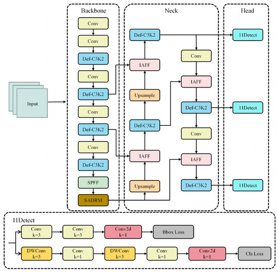
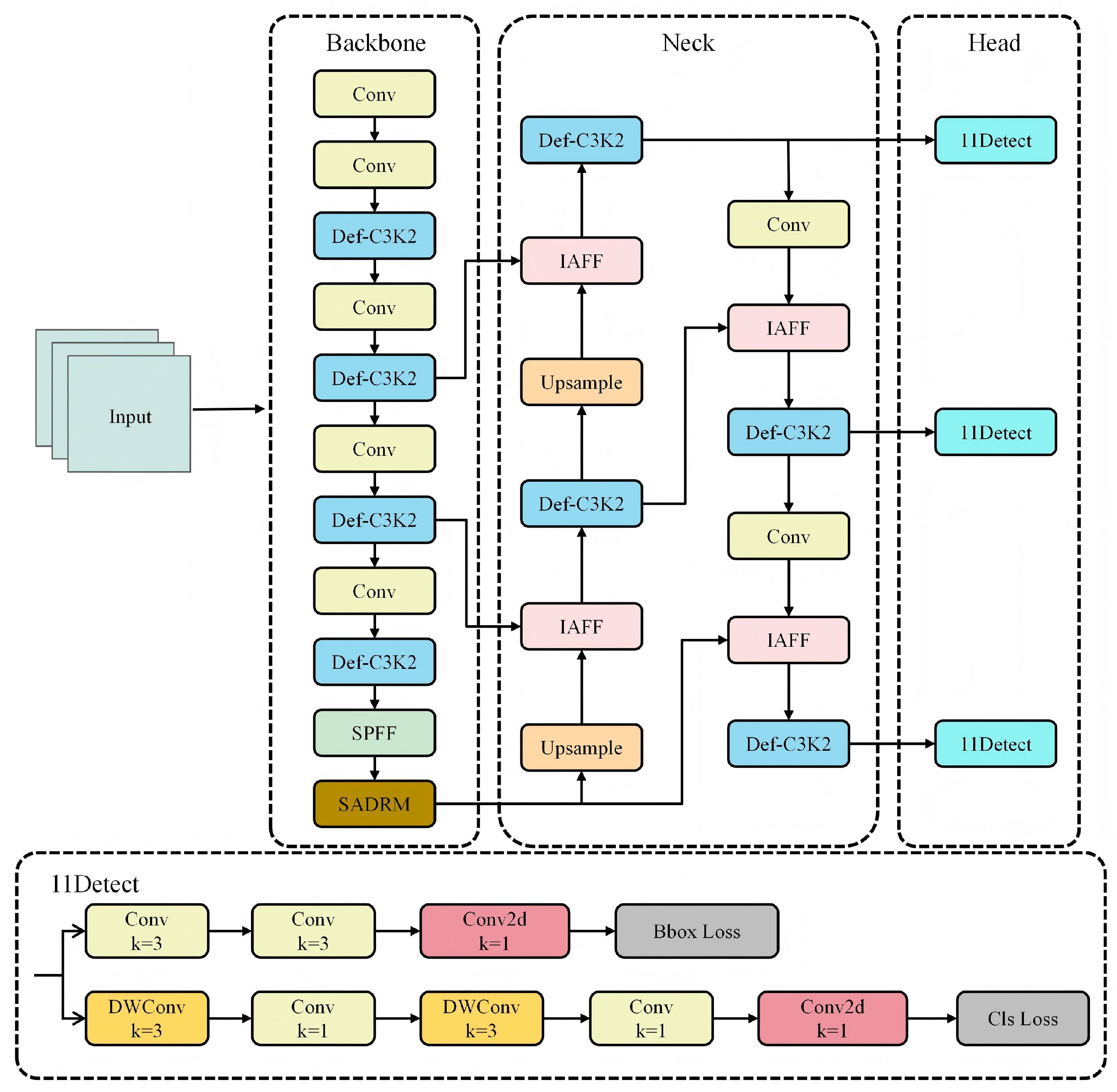
The structural design of the proposed novel DAS-YOLO framework is presented in Figure 1. This framework comprises three essential modules: a backbone network responsible for extracting features, a neck network focused on fusing multi-scale features, and a detection head committed to identifying PCB defects.
Figure 1.
DAS-YOLO network architecture diagram.
3.2. Feature Extraction Module Def-C3K2
Printed circuit board (PCB) defects exhibit core characteristics of minute target scales and extremely low pixel coverage. During multiple downsampling processes in deep networks, issues such as weakened defect feature representation and the loss of positional information readily occur [25,26]. Additionally, the standard convolutional kernels employed by the C3K2 module suffer from inherent limitations due to their rigid, fixed geometry [27]. Such rigidity prevents adaptation to the continuous curvature and irregular geometric shapes of PCB defects (e.g., broken traces), resulting in the insufficient capture of local detail features and failing to meet high-precision detection requirements.
To tackle the key challenges in PCB defect detection—including complex background interference, the easy loss of small defect features, and the difficulty in capturing asymmetric defect morphologies—this paper incorporates Deformable Convolution v4 (DCNv4). By dynamically learning spatial offsets, this convolution scheme overcomes the rigid grid sampling constraint of traditional convolutions, enabling it to adaptively accommodate the irregular geometric shapes of defects and achieve the accurate modeling of asymmetric deformation features. However, the standalone deployment of DCNv4 presents notable limitations: on the one hand, its dynamic offset calculation relies heavily on the signal-to-noise ratio (SNR) of input features. When directly applied to raw PCB feature maps, background noise is prone to inducing a large number of invalid offset calculations, which not only consumes redundant computational resources but also readily leads to localization deviations. On the other hand, DCNv4 lacks the capability to dynamically adjust the receptive field, failing to strike a balance between global context fusion and the capture of local small defects, thus capping the upper bound of feature extraction accuracy. To tackle these issues, this paper proposes the Def-UAD module, which is built on a synergistic architecture integrating 2-4-2 hierarchical dilated convolutions and DCNv4.
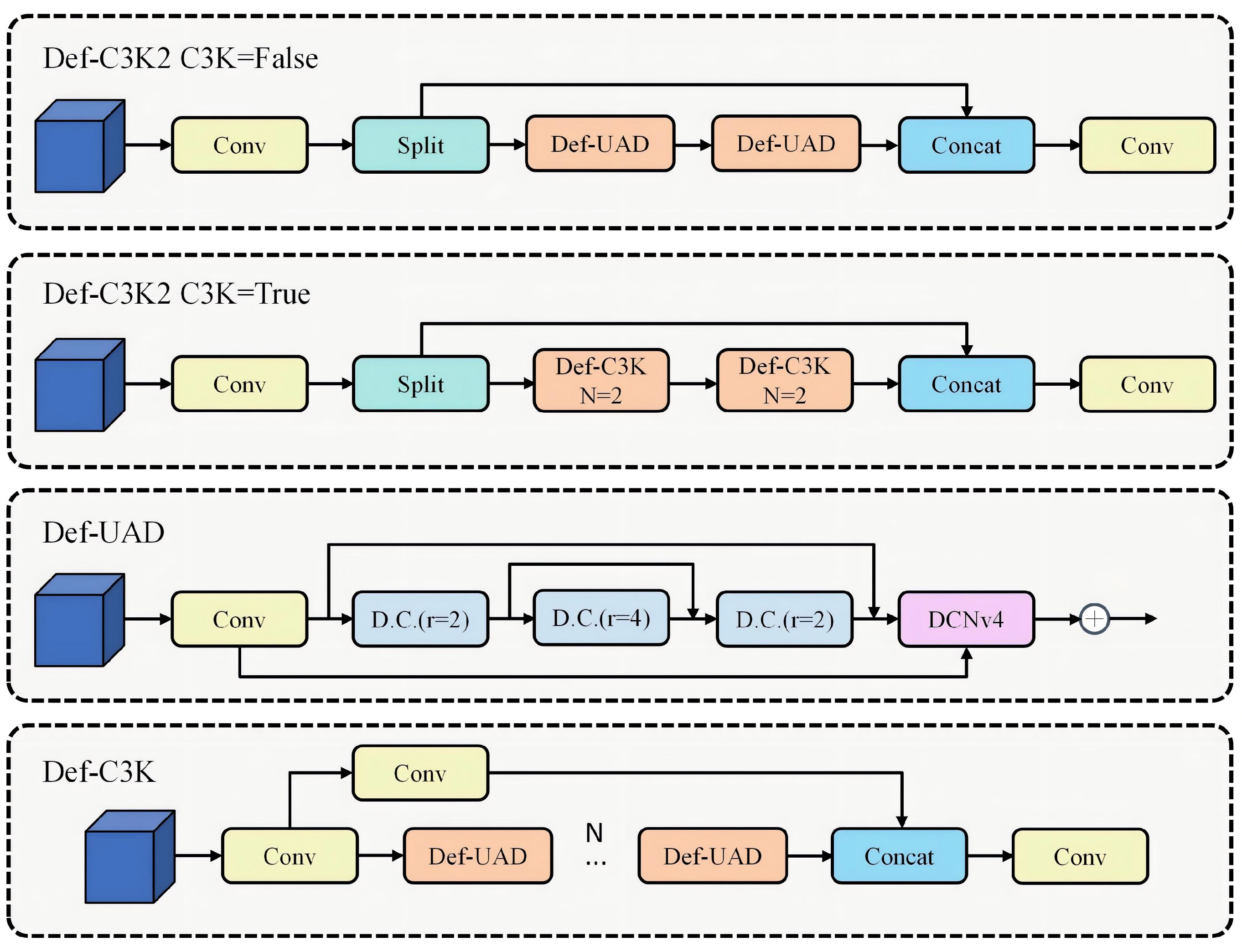
Centered around a U-shaped core framework, this module sequentially integrates one standard convolution module, three dilated convolution layers (with dilation rates of 2, 4, and 2, respectively), and one Deformable Convolution v4 (DCNv4) according to the feature processing workflow. The first layer employs a standard convolution module for preliminary feature extraction. Subsequently, the first two dilated convolution layers (dilation rates 2→4) progressively expand the receptive field, effectively integrating background scene information surrounding PCB defects while suppressing interference from complex background noise on defect features. After FOV expansion, the module contracts the FOV via a third dilated convolution layer (dilation rate 4→2) to focus on extracting fine features such as edge contours and texture transitions of PCB defects. Simultaneously, skip connections supplement lost detail information in the deep network, effectively mitigating the C3K2 module’s sensitivity to detail loss in minute targets. The module incorporates a deformable convolution v4 (DCNv4) at its end, specifically designed to address geometric symmetry breaking on PCB surfaces. Through adaptive offset sampling, this module overcomes the rigid spatial symmetry constraints of standard convolution kernels, enabling the dynamic alignment and precise detection of asymmetric defect patterns. Its comprehensive performance more significantly outperforms the design schemes of using DCNv4 alone or dilated convolution alone and better meets the requirements of PCB industrial quality inspection.
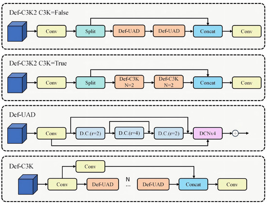
The Def-UAD module is incorporated into the C3K2 module, resulting in the enhanced Def-C3K2 structure—in which the conventional Bottleneck block is substituted with the Def-UAD module, boasting strengthened geometric perception capabilities. In practical network deployment, the C3K2 structure employs two distinct configuration modes, i.e., corresponding to the C3K = True and C3K = False configurations, respectively. Consistently, the Def-C3K2 structure retains compatibility with both configurations. The architectural diagram of the improved Def-C3K2 is illustrated in Figure 2. When the C3K parameter is set to True, the main path employs the Def-C3K module, which comprises two serially connected Def-UAD sub-modules to strengthen deep spatial modeling capabilities; when C3K is set to False, the main path directly adopts the Def-UAD module for improved efficiency and structural compactness.
Figure 2.
Def-C3K2 network architecture.
To fully harness the distinctive functionalities of the Def-C3K2 module in PCB defect detection, we purposefully incorporate it into the critical phases of the DAS-YOLO11 model’s backbone and neck networks. In the backbone network, the Def-C3K2 module replaces the original standard C3 modules in the P3, P4, and P5 stages of the YOLOv11 backbone to enhance multi-scale feature perception capabilities. Specifically, the P5 stage—characterized by deep semantic information and the largest receptive field—empowers the model to establish a robust representation of complex macro-defects within global contextual information; the P4 stage balances detailed and semantic information, effectively discriminating small-to-medium defects amid dense circuit backgrounds at the medium scale; and the P3 stage prioritizes preserving the finest spatial details and capturing subtle features of low-contrast, micron-scale defects in the early stages to mitigate information loss. This layered replacement strategy facilitates the defect-centric optimization of the backbone network, significantly enhancing its capability to perceive and characterize PCB defect features. We also fully deploy the Def-C3K2 module in the feature fusion path of the neck network, replacing the original C3 modules dedicated to feature processing and fusion in the YOLOv11 neck. This ensures that during the top-down flow and fusion of information, all processing steps inherit and reinforce the Def-C3K2 module’s unique discriminative capacity for defect-specific features. This full replacement strategy sustains high feature sensitivity and specificity toward PCB defects throughout the entire feature fusion and propagation process, thereby furnishing the detection head with a consistent, high-quality multi-scale representation of defect features.
Overall, the Def-UAD module optimizes the C3K2 module by leveraging DCNv4’s geometric adaptation and the dynamic perception strategy of dilated convolutions. This effectively resolves the structural mismatch between the inherent symmetry of standard convolution kernels and the defective asymmetric morphology in the C3K2 module while maximally preserving the integrity of deep-level semantic information during feature extraction.
3.3. SADRM
An analysis of typical image features of PCB defects reveals that defect regions share highly similar texture features with background regions, which readily gives rise to semantic ambiguity during defect discrimination. Simultaneously, defects such as stray copper and minor short circuits exhibit minimal grayscale gradient discrepancies relative to the background, accompanied by smooth boundary transitions that lack distinct gradient steps. These defects have neither clear contours nor significant grayscale variations, resulting in ambiguous boundary features that prevent models from accurately locating their spatial extent [28]. In this context, the YOLOv11 backbone network—which relies on successive downsampling operations to extract high-level semantic information—faces inherent limitations in preserving the fine-grained texture and edge details essential for defect discrimination: the subtle textures of PCB traces are progressively eroded during downsampling, with only the global features of trace regions retained. Such a downsampling-driven feature extraction paradigm fails to discriminate low-contrast, weakly delineated local defects.
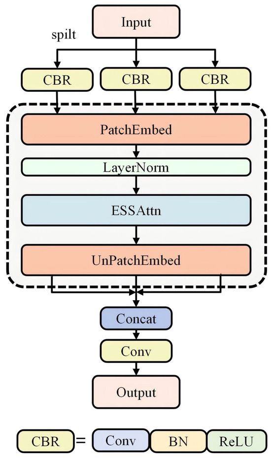
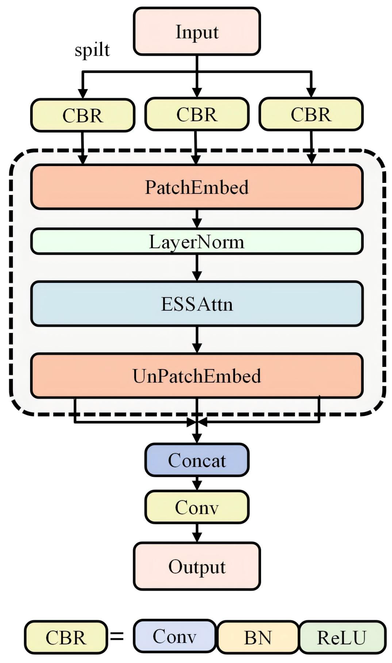
Furthermore, its feature fusion strategy relies on element-wise addition and channel concatenation, emphasizing semantic aggregation over edge modeling. Consequently, it shows inadequate responsiveness to low-contrast boundaries, rendering it difficult for the model to extract robust and consistent contour features from feature maps in weak boundary contexts [29]. To address this limitation, this paper proposes a Semantic-Aware Defensive Refinement Module (SADRM) for targeted feature refinement. Specifically, the SADRM decouples foreground, background, and uncertain regions via three-branch semantic decomposition, mitigating semantic confusion at its source. Furthermore, we propose an Edge-Sensitive Spatial Attention (ESSAttn) mechanism to highlight high-response key feature regions, thereby enabling more stable adaptive contour and texture reweighting in low-contrast, weak-boundary scenarios. Residual connections are integrated to ensure optimization stability. The SADRM’s architecture diagram is depicted in Figure 3.
Figure 3.
SADRM network architecture.
The CBR module serves as a core component in neural networks, consisting of a convolutional layer (Conv), a Batch Normalization (BN) layer, and a ReLU activation function linked sequentially. Its core function lies in providing non-linear feature transformation capability while ensuring the stable propagation of gradients during backpropagation through the BN layer.
Specifically, , , and correspond to features from the foreground, background, and uncertain regions, respectively; , , and are dedicated feature extraction modules for the foreground, background, and uncertain region, respectively.
The ESSAttn module is a feature interaction-based attention mechanism that overcomes limitations of traditional attention frameworks [30], enhancing the perception of key semantic features in FPCB defects. Its core mechanism introduces mean-centered feature vectors and energy-squared normalization: First, a linear projection layer generates three feature representations q, k, and v from the input feature map. The projection dimensions are uniformly configured to the channel dimension of the input feature maps, while the module adopts a single-head attention mechanism:
where denotes the linear layer weight matrix. Subsequently, centering processing is applied to perform mean-centered normalization on the q and k features, eliminating global offset interference between channels:
where and represent channel-wise mean values. Next, squared normalization amplifies weights for highly correlated feature pairs, enhancing the representation of important semantic features:
where . Finally, adaptive fusion combines the original feature with the attention interaction result based on squared features. This achieves the dynamic weighting and enhancement of important features, thereby improving their discriminative power.
where . The PatchEmbed module and its inverse PatchUnEmbed module jointly perform bidirectional conversion between 2D feature maps and 1D sequence representations, providing ESSAttn with compatible input/output formats. Specifically, the PatchEmbed module uses a patch size of 1 × 1 (patch size = 1) (each pixel is treated as an independent patch without spatial downsampling or aggregation):
where B (batch size) denotes the batch size; C (channels) represents the number of channels, corresponding to the channel dimension of the feature map; and (where H is the height of the feature map and W is its width) stands for the sequence length, obtained by flattening the spatial dimensions of the feature map.
The PatchUnEmbed module reconstructs the one-dimensional sequence output by ESSAttn into a two-dimensional feature map according to the original patch segmentation rules. It then adjusts the channel dimension to the target size via a 1 × 1 convolutional layer, ensuring the integrity of spatial information during the transformation process:
By leveraging bidirectional conversion between PatchEmbed and UnEmbed, we ensure the integrity of defect spatial information during feature processing. Combined with ESSAttn’s enhancement of boundary features, this approach provides clear anchors for bounding box regression, addressing YOLOv11’s weakness in handling low-contrast, blurred boundaries.
Attention enhancement is applied to the three decomposed feature branches, , , and , yielding refined features:
Finally, the refined feature maps are concatenated along the channel axis, yielding the fused feature maps. These undergo feature fusion via the channel compression module before being connected to the original input through a residual connection, yielding the following refined features:
Here, is the channel compression module, which reduces the channel dimension from to C through two layers of CBR.
3.4. Feature Fusion Module IAFF
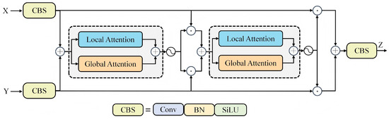
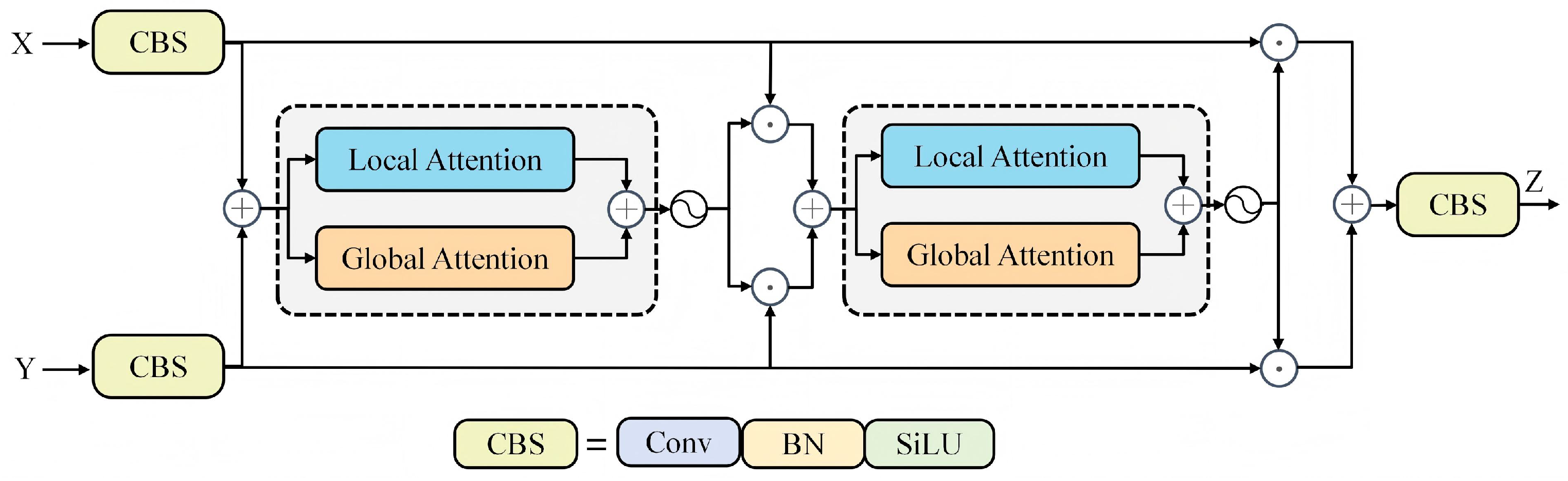
To address the inherent information asymmetry between shallow and deep feature layers, this paper proposes an Iterative Attention Feature Fusion (IAFF) module. This module dynamically calibrates cross-layer semantic and detail discrepancies via an iterative attention mechanism, thereby effectively eliminating hierarchical bias and achieving adaptive enhancement of critical defect features. As illustrated in Figure 4, the IAFF module consists of three core components: a Channel Unification Module, a Two-Stage Attention Module, and an Output Projection Module.
Figure 4.
IAFF Network Architecture.Note: ⊙ denotes element-wise multiplication; ⊕ denotes element-wise addition;  denotes Sigmoid activation function.
denotes Sigmoid activation function.
The Channel Unification Module eliminates channel mismatches between heterogeneous features by projecting input features with different channel dimensions into a unified intermediate channel space via 1 × 1 convolutions, providing consistent feature dimensions for subsequent attention computations [31]. Let the input features be and (where B is the batch size, are spatial height/width, are original channel counts, and denotes the unified intermediate channel count (default to ). The channel projection process is formulated as
These projection operations map X and Y to the shared channel dimension through 1 × 1 convolution, Batch Normalization (BN), and SiLU activation. With this consistent channel dimension established, element-wise operations can be smoothly carried out in the subsequent fusion steps.
The Two-Stage Attention Module learns adaptive feature weights in stages via a local–global dual contextual aggregation mechanism, which simultaneously enhances minute defect details (local) and large-scale defect semantics (global) [32,33].
Local attention extracts channel interactions at each spatial position via 1 × 1 convolutions, preserving low-level detail features (e.g., edges of minute scratches). The local attention is calculated as
where F represents the input feature at the current stage, and and r denote the attention reduction ratio, defaulting to 4.
Global attention compresses spatial dimensions through global average pooling (GAP) to extract channel-level global statistics, capturing large-scale defect patterns. Its calculation is
The two-stage attention mechanism refines feature weights iteratively to address the limitations of simple fusion (e.g., addition/concatenation). First, the channel-unified features are element-wise summed to obtain the initial fused feature:
Local and global attention are applied to A to generate dynamic weights normalized to the [0, 1] range via Sigmoid, which adaptively weight and to alleviate initial fusion bottlenecks:
where ⊙ denotes element-wise multiplication (Hadamard product). Stage 1 may still suffer from imprecise weight allocation (e.g., minor scratches obscured by background noise). Stage 2 takes as input to generate more refined weights , which re-weight the original unified features to enhance weak defect signals and suppress redundancy:
The Output Projection Module adjusts the fused feature to the target channel count (compatible with downstream network layers). It adopts a conditional projection strategy to avoid unnecessary computation:
The IAFF module features dynamic channel adaptation, enabling flexible embedding into any fusion node of the YOLOv11 neck FPN without modifying the original FPN channel design—this significantly reduces the engineering complexity of model improvement. Meanwhile, its lightweight design controls parameter growth, ensuring the model meets real-time detection requirements in industrial scenarios.
4. Experimentation
In this section, we conduct comparative experiments on the PCB dataset, the DsPCBSD+ dataset and the GC10-DET dataset. Our method is benchmarked against multiple baseline models and state-of-the-art algorithms, supplemented by comprehensive ablation studies to analyze results and validate the effectiveness of our approach.
4.1. Datasets
The proposed method’s effectiveness is demonstrated through validation on the PCB dataset. To assess its generalization capability, experiments were also conducted on the classic industrial surface defect dataset GC10-DET.
PCB Dataset: It comprises six defect types, specifically Missing Hole, Mouse Bite, Open Circuit, Short Circuit, Spur, and Spurious Copper, with a total of 623 samples included. The data were split into training, validation, and test subsets following an 8:1:1 split ratio.
DsPCBSD+: Provided by Guangzhou FastPrint Technology Co., Ltd., Guangzhou, Guangdong Province, China, the dataset comprises nine fine-grained defect types—including Short (SH), Spur (SP), Spurious Copper (SC), Open (OP), Mouse Bite (MB), Hole Breakout (HB), Conductor Scratch (CS), Conductor Foreign Object (CFO), and Base Material Foreign Object (BMFO)—with a total of 10,259 real-world PCB images included. This defect classification system was co-created with certified PCB quality assurance engineers to guarantee compliance with industrial quality inspection criteria.
GC10-DET: GC10 is a metal (steel plate) surface defect detection dataset focused on real industrial scenarios, serving as a classic benchmark dataset in industrial quality control. The dataset contains 10 defect categories, Punching (Pu), Weld (Wl), Crescent Gap (Cg), Water Stain (Ws), Oil Stain (Os), Silk Stain (Ss), Inclusion (In), Roll Pit (Rp), Crease (Cr), and Waist Crease (Wf), comprising 2294 images. We divided the dataset into training, validation, and test sets at an 8:1:1 ratio.
4.2. Evaluation Metrics
We evaluate four metrics: Precision, Recall, F1, and mean Average Precision (mAP@50 and mAP@50-95). The specific calculation rules are as follows:
where refers to the count of samples correctly classified as positive by the model, stands for the number of samples falsely labeled as positive, and denotes the count of samples incorrectly categorized as negative. Meanwhile, the curve represents the precision–recall curve, and N is the total number of classes in the dataset. denotes the harmonic mean of precision and recall: the higher the value (approaching 1), the superior the model’s performance. mAP@50 corresponds to the mean average precision when the IoU threshold is set to 0.5. For mAP@50-95, IoU ranges from 0.5 to 0.95 at 0.05 intervals—ten individual mAP values are computed at each step, and the final result is derived by averaging these ten metrics. Notably, IoU quantifies the overlap degree between the predicted bounding box and the ground truth bounding box. For inference, the model was executed using FP32 inference to maintain full accuracy during evaluation.
During the experiment, the training was conducted for 400 epochs with a batch size of 8 and an initial learning rate of 0.001. The input resolution was set to 640 pixels, and data augmentation was performed using a hybrid approach. The NMS threshold was set to 0.7 for post-processing. All experiments were run on a single NVIDIA RTX 2080 Ti GPU with 11 GB VRAM. The detailed hardware configuration and training strategy, including all key parameters, are summarized in Table 1.
Table 1.
Hardware configuration and training strategy.
4.3. Comparative Experiments
4.3.1. Result in PCB Defect Dataset
We selected the most widely used foundational models in industrial surface defect detection for comparison, including YOLOv5, YOLOv8, YOLOv9, YOLOv10, and YOLOv11. All YOLO models employed are of the “n” variant. Additionally, to validate the advanced nature of our approach, we compared it against several state-of-the-art surface defect detection algorithms: (1) FPDNet, a network designed to address size variations and low defect contrast; (2) SLF, a lightweight detection network for small-target defects; (3) SRN, a small-object detection framework for PCB defect detection; (4) GD-YOLO, a lightweight surface defect detection network; and (5) PCB-FS [34], an integrated frequency–spatial fusion learning framework that enhances YOLOv8 by integrating three complementary functional modules.
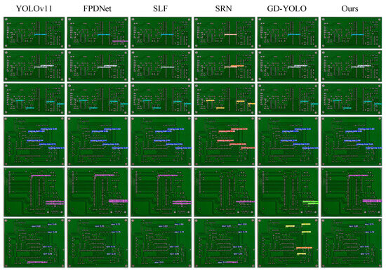
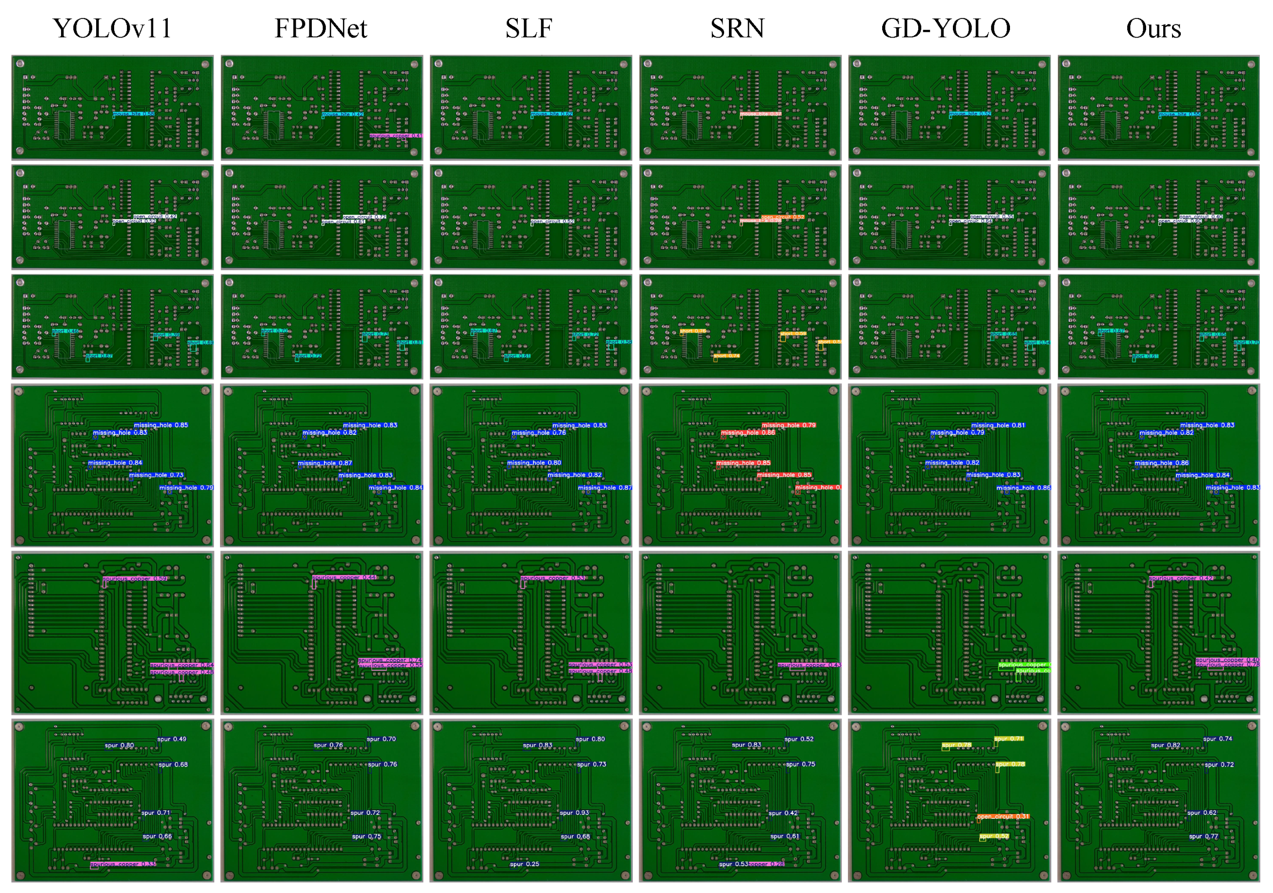
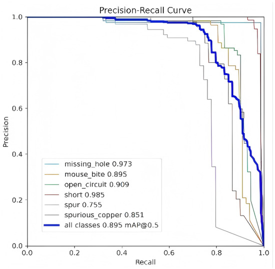
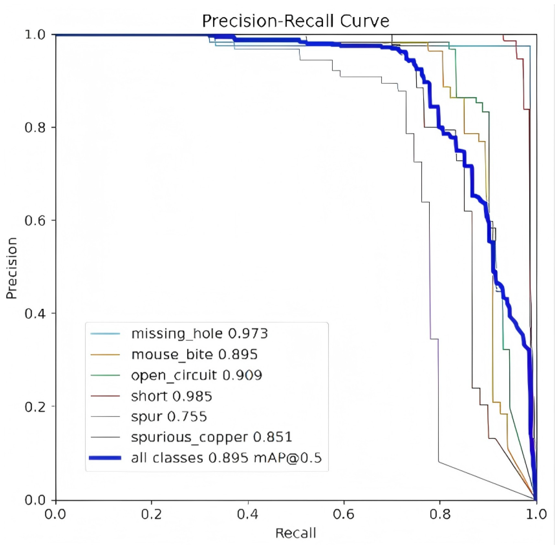
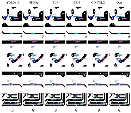
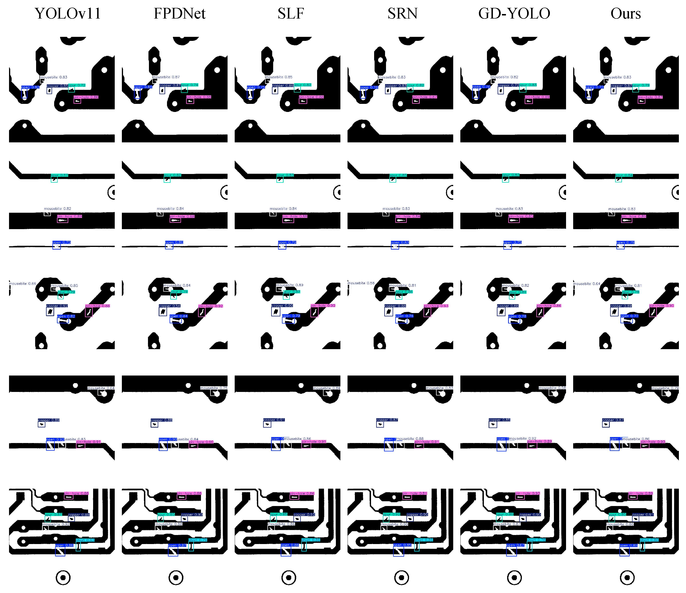
As shown in Table 2, our method achieves significant improvements over the baseline YOLOv11 model. The experimental results obtained under various random seeds are presented in the Supplementary Material, Tables S1–S4. Recall increases by 3.7% to 0.826, indicating that our approach maintains high detection rates while reducing missed detections. Regarding mAP@50 and mAP@50-95 metrics, our approach achieves 0.895 and 0.466, respectively, representing improvements of 1.8% and 2.9% over the baseline model. This highlights the distinct advantages of our proposed method in terms of accurate defect localization and the effective handling of overlapping defects. Furthermore, our approach exhibits substantial superiority compared to other advanced surface defect detection methods. Compared to GD-YOLO, our method improves mAP@ 50 and mAP@50-95 by 2.4% and 2.6%. Compared to SRN, our method improves mAP@ 50 and mAP@50-95 by 7.8% and 4.9%. The experimental results demonstrate that our method achieves more accurate defect identification in PCB defect detection. Detection results from the baseline model, our method, and several other state-of-the-art approaches are shown in Figure 5. Figure 6 presents the category-wise and overall PR curves, along with the AP for each class and mAP@0.5 for the entire dataset. This visualization is fundamental for assessing the model’s classification efficacy. It is evident from the figure that the overall PR curve achieves an mAP@0.5 of 0.895. The model demonstrates high precision when recall is below 0.6. For higher recall rates, a characteristic decline in precision is observed, reflecting the inherent trade-off. This overall performance highlights the model’s robust comprehensive detection capabilities.
Table 2.
Comparison of DAS-YOLO with multiple surface defect detection models on PCB.
Figure 5.
Detection results of multiple models on the PCB dataset.
Figure 6.
Precision–recall curves for DAS-YOLO on PCB surface defect detection.
4.3.2. Result in DsPCBSD+
To validate the generalizability of our approach, we conducted comparative experiments on DsPCBSD+ using the same configuration. The experimental results are summarized in Table 3.
Table 3.
Comparison of DAS-YOLO with multiple surface defect detection models on DsPCBSD+.
As shown in Table 3, our method achieves significant improvements over the baseline YOLOv11 model. Recall increases by 1.6% to 0.974, indicating that our approach maintains high detection rates while reducing missed detections. Regarding mAP@50 and mAP@50-95 metrics, our approach achieves 0.991 and 0.783, respectively, representing improvements of 0.2% and 4.5% over the baseline model. This highlights the distinct advantages of our proposed method in terms of accurate defect localization and the effective handling of overlapping defects. Furthermore, our approach exhibits substantial superiority compared to other advanced surface defect detection methods. Compared to PCB-FS, our method improves mAP@ 50 and mAP@50-95 by 0.2% and 1.2%. Compared to SRN, our method improves mAP@ 50 and mAP@50-95 by 0.4% and 0.1%. The experimental results demonstrate that our method achieves more accurate defect identification in PCB defect detection. Detection results from the baseline model, our method, and several other state-of-the-art approaches are shown in Figure 7.
Figure 7.
Detection results of multiple models on DsPCBSD+.
4.3.3. Result in GC10-DET
To validate the generalizability of our approach, we conducted comparative experiments on the GC10-DET using the same configuration. The experimental results are summarized in Table 4.
Table 4.
Comparison of experimental results in terms of detection accuracy on GC10-DET.
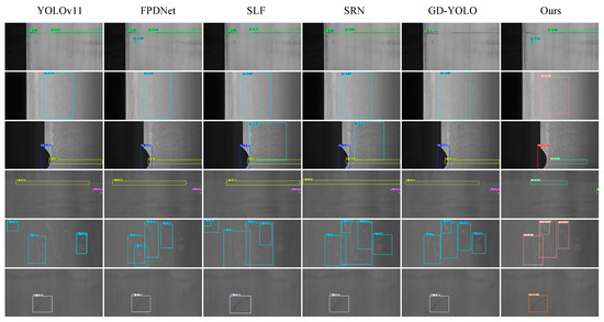
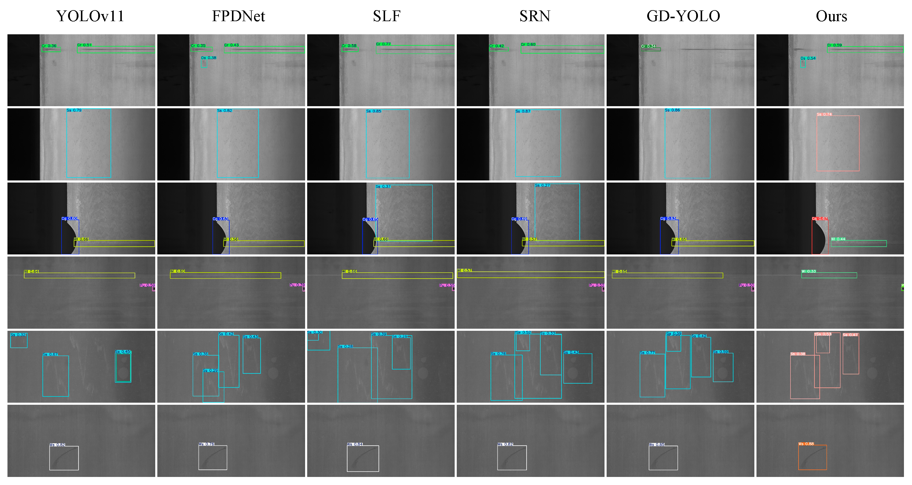
As shown in Table 4, our method achieves significant improvements over the baseline YOLOv11 model. Precision and recall are increased by 1.1% and 1.6% respectively, reaching 0.731 and 0.604. This demonstrates that our approach maintains high detection rates while avoiding missed detections. For mAP@50 and mAP@50-95 metrics, our method achieves 0.667 and 0.346, respectively, representing 3.4% and 2.0% improvements over the baseline model. This demonstrates the distinct advantages of our proposed method in the precise localization and strict control of overlapping defects. Additionally, our approach exhibits substantial advantages over other advanced surface defect detection methods. Compared to GD-YOLO, our method improves mAP@ 50 and mAP@50-95 by 13.1% and 7.7%. Compared to SRN, our method improves mAP@50 by 3.7%. The experimental results demonstrate that our method not only excels in PCB defect detection but also maintains high detection accuracy for other industrial surface defects. Detection results from the baseline model, our method, and several other advanced approaches are shown in Figure 8.
Figure 8.
Detection results of multiple models on the GC10-DET dataset.
4.4. Ablation Experiments
To further verify the effectiveness of individual modules within the proposed approach, ablation studies were performed on the PCB dataset, with the corresponding findings summarized in Table 5. After introducing the Def-C3k2 module, mAP@50 improved significantly, though precision decreased slightly. Notably, when the SADRM was introduced alone, mAP@50 showed a noticeable decline, while recall saw a substantial increase. This indicates that the model traded off precision for gains in recognition comprehensiveness. When using the IAFF module alone, both mAP@50 and mAP@50-95 achieved moderate improvements. When all three modules are used concurrently, the model achieves substantial gains in recall and recognition accuracy while maintaining precision. This enables the model to process each defect with greater accuracy and comprehensiveness. Specifically, when the SADRM was integrated in isolation, it demonstrated a substantial increase in recall, signifying an enhanced ability to detect a wider range of defects. However, this came at the cost of a slight decrease in precision, which consequently led to a noticeable decline in mAP@50. This behavior clearly indicates that the SADRM, when operating independently, favors comprehensiveness (higher recall) over strict precision, effectively expanding the model’s detection scope. Therefore, the SADRM’s core contribution lies in its capability to significantly boost the model’s recall, especially for challenging defect scenarios, acting as a crucial component for ensuring comprehensive defect recognition. While its isolated application presents a precision–recall trade-off, its full value is realized within the complete DAS-YOLO framework, where its recall-enhancing effect is synergistically complemented by Def-C3k2 and IAFF. As seen in the full model (DAS-YOLO), the SADRM contributes to achieving an mAP@50 of 0.895 and a recall of 0.826, surpassing the base model in both metrics.
Table 5.
Results of ablation experiments on PCB defect detection dataset.
5. Conclusions
This paper addresses the challenges in printed circuit board (PCB) defect detection—such as diverse defect types, low contrast, and minuscule detection targets—by proposing an improved PCB defect detection algorithm named DAS-YOLO. Built on the YOLOv11 framework, the proposed algorithm realizes comprehensive performance improvements through multidimensional optimizations. The specific optimizations are detailed as follows:
First, the U-shaped adaptive feature extraction module (Def-UAD) replaces the standard convolutional units within the C3K2 module. By incorporating skip connections and deformable convolutions v4 (DCNv4), it restores lost detail information in deep networks, thereby enhancing the C3K2 module’s ability to extract features from PCB defects. The SADRM replaces the original C2PSA module. Employing ternary semantic decomposition enables refined feature segmentation to capture more comprehensive contextual information, preventing data gaps and further enhancing model accuracy. Finally, by replacing the model’s original concatenation structure, the improved iterative attention feature fusion module (IAFF) effectively resolves the information distribution asymmetry between deep and shallow features, achieving the dynamic fusion and enhancement of multi-scale features.
To validate the effectiveness of each improvement, ablation and comparative experiments were conducted on the public PCB dataset. The results show the proposed model achieves a recall of 0.826 and mAP@50 and mAP@50-95 of 0.895 and 0.466, representing improvements of 3.7%, 1.8%, and 2.9% over the baseline model. Furthermore, a comparative analysis with mainstream surface defect detection algorithms (e.g., GD-YOLO, SRN) further validated the superiority of the improved model. To evaluate the model’s generalization performance, supplementary experiments were carried out on the public GC10-DET dataset for steel defects, validating the improved algorithm’s reliable performance and strong adaptability. This paper addresses challenges in PCB defect detection, including low contrast, minute detection targets, and complex detection tasks. Subsequent research will prioritize lowering model complexity and reducing computational overhead without compromising detection precision.
Supplementary Materials
The following supporting information can be downloaded at: https://www.mdpi.com/article/10.3390/sym18020222/s1, Table S1: Comparison of DAS-YOLO with multiple surface defect detection models on PCB, based on experiments with random seed 2026; Table S2: Comparison of DAS-YOLO with multiple surface defect detection models on PCB, based on experiments with random seed 2026; Table S3: Comparison of DAS-YOLO with multiple surface defect detection models on PCB, based on experiments with random seed 2026; Table S4: Comparison of models on PCB dataset: Mean metrics from different random seeds.
Author Contributions
Methodology, W.W. and W.J.; software, W.W. and L.Z.; validation, W.W. and S.C.; investigation, W.W., W.J. and Q.Z.; resources, L.Z. and W.J.; writing—original draft preparation, W.W., W.J. and S.C.; writing—review and editing, L.Z., W.J. and Q.Z.; supervision, L.Z., W.J. and S.C.; and project administration, L.Z. and W.J. All authors have read and agreed to the published version of the manuscript.
Funding
This research was sponsored by the Special Fund for Major Scientific and Technological Achievements Transformation in Jiangsu Province (grant number: BA2023044).
Data Availability Statement
The data presented in this study are not publicly available due to the confidentiality requirements of cooperative research projects, but are available on demand from the corresponding author or first author at zhanglihua@just.edu.cn or wweipan@stu.just.edu.cn.
Acknowledgments
The authors thank the anonymous reviewers for providing critical comments and suggestions that improved the manuscript. DeepL Translate (Version 5.0) was used for Chinese-to-English translation, and Grammarly Premium (Version 2025) for English language polishing; no other AI or AI-assisted tools were used in the manuscript preparation.
Conflicts of Interest
The authors declare no conflicts of interest.
References
- Park, J.-H.; Kim, Y.-S.; Seo, H.; Cho, Y.-J. Analysis of Training Deep Learning Models for PCB Defect Detection. Sensors 2023, 23, 2766. [Google Scholar] [CrossRef] [Scilit] [PubMed]
- Zheng, J.; Sun, X.; Zhou, H.; Tian, C.; Qiang, H. Printed circuit boards defect detection method based on improved fully convolutional networks. IEEE Access 2022, 10, 109908–109918. [Google Scholar] [CrossRef] [Scilit]
- Ali, M.L.; Zhang, Z. The YOLO framework: A comprehensive review of evolution, applications, and benchmarks in object detection. Computers 2024, 13, 336. [Google Scholar] [CrossRef] [Scilit]
- Khanam, R.; Hussain, M. Yolov11: An overview of the key architectural enhancements. arXiv 2024, arXiv:2410.17725. [Google Scholar] [CrossRef] [Scilit]
- Zou, C.; Yu, S.; Yu, Y.; Gu, H.; Xu, X. Side-scan sonar small objects detection based on improved YOLOv11. J. Mar. Sci. Eng. 2025, 13, 162. [Google Scholar] [CrossRef] [Scilit]
- Wang, C.; Song, X.; Wang, J.; Yan, X. An improved YOLOv11 algorithm for small object detection in UAV images. Signal Image Video Process. 2025, 19, 507. [Google Scholar] [CrossRef] [Scilit]
- Wang, F.; Jiang, X.; Han, Y.; Wu, L. YOLO-LSDI: An Enhanced Algorithm for Steel Surface Defect Detection Using a YOLOv11 Network. Electronics 2025, 14, 2576. [Google Scholar] [CrossRef] [Scilit]
- Selvam, P.; Rajasekar, R.; Gunasundari, C.; Priya, S.J.; Murugappan, M.; Chowdhury, M.E. YOLO-DefXpert: An Advanced Defect Detection on PCB Surfaces Using Improved YOLOv11 Algorithm. IEEE Access 2025, 13, 143085–143101. [Google Scholar] [CrossRef] [Scilit]
- Shen, P.; Mei, K.; Cao, H.; Zhao, Y.; Zhang, G. LDDFSF-YOLO11: A Lightweight Insulator Defect Detection Method Focusing on Small-sized Features. IEEE Access 2025, 13, 90273–90292. [Google Scholar] [CrossRef] [Scilit]
- Shi, W.; Dai, J.; Li, C.; Niu, N. YOLOv11-EMD: An Enhanced Object Detection Algorithm Assisted by Multi-Stage Transfer Learning for Industrial Steel Surface Defect Detection. Mathematics 2025, 13, 2769. [Google Scholar] [CrossRef] [Scilit]
- Sheng, W.; Zhao, J.; Chen, Q. SNEIF-YOLO11: A Lightweight real-time framework for fighting behavior detection. Signal Image Video Process. 2025, 19, 1121. [Google Scholar] [CrossRef] [Scilit]
- Chen, S.; Li, W.; Yan, X.; Liu, W.; Chen, C.; Liao, J.; Shu, J. Research on low contrast surface defect detection method based on improved YOLOv7. IEEE Access 2024, 12, 179997–180008. [Google Scholar] [CrossRef] [Scilit]
- Ji, Y.; Zhang, D.; He, Y.; Zhao, J.; Duan, X.; Zhang, T. Improved YOLO11 Algorithm for Insulator Defect Detection in Power Distribution Lines. Electronics 2025, 14, 1201. [Google Scholar] [CrossRef] [Scilit]
- Lan, X.; Wang, X.; Liu, L. RMC-YOLO: An Object Detection Model for Insulator Defects. Signal Image Video Process. 2025, 19, 1033. [Google Scholar] [CrossRef] [Scilit]
- Chen, Q.; Ong, Q.; Huang, H.; Tang, S. An Efficient and Lightweight Surface Defect Detection Method for Micro-Motor Commutators in Complex Industrial Scenarios Based on the CLS-YOLO Network. Electronics 2025, 14, 505. [Google Scholar] [CrossRef] [Scilit]
- Wang, Z.; Su, Y.; Kang, F.; Wang, L.; Lin, Y.; Wu, Q.; Cai, Z. PC-YOLO11s: A lightweight and effective feature extraction method for small target image detection. Sensors 2025, 25, 348. [Google Scholar] [CrossRef] [Scilit]
- Luo, Y.; Wu, A.; Fu, Q. MAS-YOLOv11: An improved underwater object detection algorithm based on YOLOv11. Sensors 2025, 25, 3433. [Google Scholar] [CrossRef] [Scilit]
- He, J.; Yuan, B.; Guo, C.; Li, H.; Wang, F.; Chu, P.; Guo, H. KL-YOLO: A Lightweight Adaptive Global Feature Enhancement Network for Small Object Detection in Low-Altitude Remote Sensing Imagery. IEEE Trans. Instrum. Meas. 2025, 74, 5037213. [Google Scholar]
- Mo, C.; Hu, Z.; Wang, J.; Xiao, X. SGT-YOLO: A Lightweight Method for PCB Defect Detection. IEEE Trans. Instrum. Meas. 2025, 74, 3543911. [Google Scholar] [CrossRef] [Scilit]
- Ong, S.K.; Tan, C.K.; Baskaran, V.M.; Puah, B.K.; Liew, K.H. Enhancing Industrial PCB and PCBA Defect Detection: An Efficient and Accurate SEConv-YOLO Approach. IEEE Access 2025, 13, 148917–148935. [Google Scholar] [CrossRef] [Scilit]
- Ge, Q.; Wu, R.; Wu, Y.; Liu, H. A Class-Incremental Learning Method for PCB Defect Detection. IEEE Trans. Instrum. Meas. 2025, 74, 2508515. [Google Scholar] [CrossRef] [Scilit]
- Zhang, T.; Zhang, J.; Pan, P.; Zhang, X. YOLO-RRL: A lightweight algorithm for PCB surface defect detection. Appl. Sci. 2024, 14, 7460. [Google Scholar] [CrossRef] [Scilit]
- Li, K.; Zhong, X.; Han, Y. A High-performance Small Target Defect Detection Method for PCB Boards Based on a Novel YOLO-DFA Algorithm. IEEE Trans. Instrum. Meas. 2025, 74, 2008312. [Google Scholar] [CrossRef] [Scilit]
- He, X.; Xie, M. ABF-YOLO: A Fine-Grained PCB Defect Detection Framework Integrating Axial Attention and Bidirectional Feature Fusion. IEEE Trans. Consum. Electron. 2025, 71, 8562–8570. [Google Scholar] [CrossRef] [Scilit]
- Lin, T.Y.; Dollár, P.; Girshick, R.; He, K.; Hariharan, B.; Belongie, S. Feature pyramid networks for object detection. In Proceedings of the IEEE Conference on Computer Vision and Pattern Recognition, Honolulu, HI, USA, 21–26 July 2017; pp. 2117–2125. [Google Scholar]
- Wang, J.; Sun, K.; Cheng, T.; Jiang, B.; Deng, C.; Zhao, Y.; Mao, B. Deep high-resolution representation learning for visual recognition. IEEE Trans. Pattern Anal. Mach. Intell. 2020, 43, 3349–3364. [Google Scholar] [CrossRef] [Scilit] [PubMed]
- Zhu, X.; Hu, H.; Lin, S.; Dai, J. Deformable convnets v2: More deformable, better results. In Proceedings of the IEEE/CVF Conference on Computer Vision and Pattern Recognition, Long Beach, CA, USA, 15–20 June 2019; pp. 9308–9316. [Google Scholar]
- Roth, K.; Pemula, L.; Zepeda, J.; Schölkopf, B.; Brox, T.; Gehler, P. Towards total recall in industrial anomaly detection. In Proceedings of the IEEE/CVF Conference on Computer Vision and Pattern Recognition, New Orleans, LA, USA, 19–24 June 2022; pp. 14318–14328. [Google Scholar]
- Tan, M.; Pang, R.; Le, Q.V. Efficientdet: Scalable and efficient object detection. In Proceedings of the IEEE/CVF Conference on Computer Vision and Pattern Recognition, Seattle, WA, USA, 13–19 June 2020; pp. 10781–10790. [Google Scholar]
- Zhang, M.; Zhang, C.; Zhang, Q.; Guo, J.; Gao, X.; Zhang, J. ESSAformer: Efficient transformer for hyperspectral image super-resolution. In Proceedings of the IEEE/CVF International Conference on Computer Vision, Paris, France, 2–6 October 2023; pp. 23073–23084. [Google Scholar]
- Wang, X.; Girshick, R.; Gupta, A.; He, K. Non-local neural networks. In Proceedings of the IEEE Conference on Computer Vision and Pattern Recognition, Salt Lake City, UT, USA, 18–23 June 2018; pp. 7794–7803. [Google Scholar]
- Chen, Y.; Kalantidis, Y.; Li, J.; Yan, S.; Feng, J. A2-nets: Double attention networks. Adv. Neural Inf. Process. Syst. 2018, 31, 1–10. [Google Scholar]
- Chu, X.; Tian, Z.; Wang, Y.; Zhang, B.; Ren, H.; Wei, X.; Shen, C. Twins: Revisiting spatial attention design in vision transformers. arXiv 2021, arXiv:2104.13840. [Google Scholar]
- Wang, S.; Li, B.; Zheng, F.; Zhang, Y. PCB-FS: Frequency–Spatial Feature Learning for PCB Defect Detection. Symmetry 2025, 17, 2020. [Google Scholar] [CrossRef] [Scilit]

Disclaimer/Publisher’s Note: The statements, opinions and data contained in all publications are solely those of the individual author(s) and contributor(s) and not of MDPI and/or the editor(s). MDPI and/or the editor(s) disclaim responsibility for any injury to people or property resulting from any ideas, methods, instructions or products referred to in the content. |
© 2026 by the authors. Licensee MDPI, Basel, Switzerland. This article is an open access article distributed under the terms and conditions of the Creative Commons Attribution (CC BY) license.