


Abstract
Two-dimensional (2D) layered materials—graphene, hexagonal boron nitride (hBN), transition metal dichalcogenides (TMDs), and layered van der Waals (vdW) thiophosphates—constitute a rapidly expanding family whose properties are governed by weak van der Waals interlayer coupling and strong intralayer bonding. This review surveys the principal classes of 2D layered materials and systematically pairs each class with the low-frequency noise (LFN) spectroscopy studies performed on it mainly between 2013 and 2026. Unlike earlier material-specific reviews, it systematically compares the experimental device configurations, assigned microscopic mechanisms, and research gaps. The review also identifies specific research priorities.
1. Introduction
The year 2025 marked the centenary of the discovery of so-called 1/f noise. In 1925, J. B. Johnson successfully measured electrical noise in vacuum tubes during his time at Bell Labs [1]. During his experiments, he discovered an unexpected extra noise that became stronger at low frequencies. This was also called low-frequency noise (LFN), “flicker noise”, or 1/f noise.
Over the following decades, scientists noticed the same strange behavior in many different devices. The strength of the noise changed according to the formula f −α (where α is between 0.5 and 1.5), and it could be seen across a very wide range of frequencies—in some thin-film resistors and even across more than six frequency decades—and the noise never flattened out at low frequencies. In the 1980s, scientists proposed several explanations, but in the end, it was agreed: there is no single general theory that explains 1/f noise—in different materials it comes from different causes. But, surprisingly, it was exactly this lack of universality that made noise a useful tool. During the 1990s, 1/f noise became an important way to check the quality and reliability of electronic devices [2,3]. By the early 2000s, noise spectroscopy had become a recognized method in materials science—used to study defects in metals, electronic phase separation in manganites, percolation in composites, and oxygen movement in oxides.
The field also has a long institutional history. A dedicated international conference series has been held every two years since 1968. It began as the “Fluctuation Phenomena” and “Noise in Physical Systems” meetings, which later merged with the 1/f noise symposia; the proceedings of the 16th conference (2001) were still published under the title Noise in Physical Systems and 1/f Fluctuations. In the early 2000s the series adopted its present name—the International Conference on Noise and Fluctuations (ICNF). Recent editions of the series have been held in Prague (2003), Salamanca (2005), Tokyo (2007), Pisa (2009), Toronto (2011), Montpellier (2013), Xi’an (2015), Vilnius (2017), Neuchâtel (2019), and Grenoble (2023). Today, noise spectroscopy is explicitly advocated for monitoring phase transitions, tracking material degradation and assessing material and device quality.
In this review, graphene and principal classes of two-dimensional layered-structure materials (hBN, TMDs, CuInP2S6) are presented together with the low-frequency noise spectroscopy performed on each. This review does not aim to provide an exhaustive survey of all layered two-dimensional (2D) materials. Instead, it focuses on representative material classes for which low-frequency noise spectroscopy has been most extensively developed and experimentally validated. Graphene, hexagonal boron nitride, transition metal dichalcogenides, and layered thiophosphates were selected because together they cover conductive, insulating, semiconducting, and ferroic layered systems, allowing the diverse roles of noise spectroscopy—from defect characterization and transport studies to phase-transition diagnostics—to be compared within a unified framework.
2. Literature Search Strategy
This paper presents a narrative review of recent advances in low-frequency noise spectroscopy of low-dimensional layered materials. A structured literature search was conducted using Web of Science, Scopus, and PubMed, covering publications mainly from 2015 to 2026. To focus the analysis on developments reported in the primary literature and to avoid duplicating previously published syntheses, review articles were excluded from the formal literature search and subsequent analysis. Priority was given to original peer-reviewed research articles directly addressing low-frequency noise phenomena in low-dimensional layered materials and related devices. Earlier review articles were used only for general background and scope definition and were not included in the analyzed literature set.
The search strategy utilized combinations of noise-related and material-related keywords: (“low-frequency noise” OR “1/f noise” OR “noise spectroscopy”) AND (“two-dimensional material” OR “2D material” OR “layered material” OR “van der Waals crystal” OR “graphene” OR “transition metal dichalcogenide” OR “TMD” OR “hexagonal boron nitride” OR “hBN” OR “thiophosphate” OR “CuInP2S6”).
Studies were selected based on defined inclusion criteria. Inclusion criteria comprised (1) peer-reviewed original research articles, book chapters, and conference abstracts; (2) studies directly investigating either (a) the physical mechanisms underlying low-frequency noise in low-dimensional layered materials or (b) the challenges and strategies associated with low-frequency noise reduction in related devices; and (3) papers reporting clear experimental or theoretical findings. Google Scholar Labs was additionally used as an AI-assisted tool for preliminary relevance screening. The query-specific descriptions generated by the tool were used to identify potentially relevant studies. Final eligibility decisions were based on the evaluation of article titles, abstracts, and, where necessary, full texts, rather than solely on AI-generated descriptions.
3. Low-Frequency Noise Spectroscopy in Materials Research
Electronic noise is classified into four intrinsic types: thermal (Johnson–Nyquist) noise, which is material-independent and useful mainly for calibration; shot noise; generation–recombination (G-R) noise with Lorentzian spectra of individual trapping states; and flicker (1/f) noise, whose specific physical mechanism is not generally accepted [3].
Low-frequency noise is a ubiquitous phenomenon observed across a remarkably wide range of systems—from current fluctuations in resistors to intensity fluctuations in music and even signals in human cognition. In electronics, this phenomenon, known as 1/f noise, flicker noise, or excess noise, hampers the operation of numerous devices and circuits and can be a significant impediment to developing practical applications from new materials. At the same time, the very same noise serves as a valuable diagnostic tool: the study of slow time-varying resistance fluctuations offers deep insight into electronic transport and scattering mechanisms, and also acts as a device-performance benchmark.
This subject is extensively covered in several substantial review articles worth reading and citing. The more classic reviews of low-frequency noise in electronic systems include [2,3,4,5,6,7]. These largely focused on identifying noise as a defect signature. Since the theoretical background of noise has been exhaustively covered in these comprehensive reviews, we find it unnecessary to reiterate it in this paper. In review [8], systematized prior efforts in using noise spectroscopy as a diagnostic tool in materials science were reported, covering metal films, semiconductors, metallic oxides, and inhomogeneous systems such as composites and percolating systems. The review also gives many practical examples, including the identification of defects and their activation energies. Raychaudhuri’s paper can be considered an encouragement for the wider application of noise spectroscopy in materials science. Furthermore, two subsequent papers examining noise separately in graphene [9] and van der Waals materials [10] were published later, serving as evidence that this field is gradually expanding. A concise introductory overview of noise theory can be found in [9]. A more comprehensive discussion of the models describing the origin of noise can be found in [10].
4. Classification of 2D Layered Materials
Discovered in 2004, the new material graphene now occupies one of the most important places in materials science and nanotechnology. Graphene is a layer one carbon atom thick, whose two-dimensional crystal lattice resembles a honeycomb structure. This material exhibits exceptionally good properties: high electron mobility at room temperature (250,000 cm2/Vs), high thermal conductivity (5000 W m−1 K−1), and enormous mechanical strength (Young’s modulus ~1 TPa) [11]. A little more than a decade after the first report on the isolation and characterization of two-dimensional graphene, the family of two-dimensional materials was joined by many new members. By successfully applying the experience and knowledge gained while studying graphene, and using those same fabrication methods (mechanical exfoliation, CVD, etc.), new two-dimensional single crystals were synthesized, exhibiting unique properties that extend the possibilities of 2D materials. Materials such as hexagonal boron nitride (hBN), silicene, germanene and others were discovered. In addition, layered semiconductors (Bi2Se3, GaSe) and oxides (TiO2, MoO3) as well as transition metal dichalcogenides (MoS2, WS2) and trichalcogenides are also classified as two-dimensional (2D) structure-type materials.
5. Graphene
Graphene is the ancestor material in the 2D family, both for its structure and its history [11]. Graphene research papers are characterized by very high citation rates [12,13,14]. Since the isolation of the single graphene layer in 2004, the research field emerged almost overnight, and the number of papers grew exponentially [15]. One of the most important papers in this field is A. K. Geim and K. S. Novoselov’s “The rise of graphene” (2007) [16], which was cited 11,102 times in one decade (2001–2010) [12]. This paper is often considered together with their earlier 2004 Science publication, “Electric field in atomically thin carbon films”, since both studies laid the foundation for graphene research that led to the Nobel Prize in 2010. Since 2014, the total number of graphene papers roughly doubled, but the number of papers related specifically to manufacturing has remained relatively stable [13]. This may be because industrial results became commercial secrets or patents. In the later period (2015–2021), graphene oxide publications increased significantly (81.3%), reaching a peak in 2021 with 5469 papers per year.
Graphene is also important in noise research. Historically, continuous metal or semiconductor films could not be fabricated with uniform thickness below approximately 8 nm, which prevented a direct test of where LFN originates. High-quality graphene and multilayer graphene structures overcome this limitation, since their thickness can be tuned continuously and uniformly from a graphite-like bulk all the way down to a single atomic layer, which represents the ultimate surface limit. The first report of LFN in graphene appeared in 2008 [17]. The study found that the LFN is substantially lower in bilayer graphene (BLG) than in single layer graphene (SLG), and that in monolayer graphene the noise follows Hooge’s empirical relation. Low-frequency noise (LFN) in graphene has been widely studied since then. A comprehensive review of this field, covering the main physical mechanisms, experimental data, and applications up to 2013, is provided in the work by Balandin (2013) [9] and the literature cited therein.
That review identifies two principal challenges in low-noise graphene research. The first is a long-standing debate in electronics over the origin of LFN—a question that is particularly important for device scaling, since noise levels typically increase as device dimensions are reduced. The second is the practical goal of noise reduction, which is essential for improving the performance of future graphene devices. The present section focuses mainly on more recent studies (2013–2026) that have complemented these earlier findings or attempted to answer these questions.
B. Pellegrini proposed a comprehensive model of LFN in nanoscale graphene devices that reproduces the unusual dependence of the noise power spectral density on carrier concentration [18]. By computing the coupling between trap charge fluctuations and the terminal current via an extension of the electrokinematics theorem to two-dimensional devices, the model attributes LFN to charge trapping–detrapping in defects with a broad distribution of relaxation times. It accounts for the experimentally observed evolution of the noise shape—from M to Λ type in single-layer sheets as material inhomogeneity increases, and a V shape in bilayer sheets—and predicts that noise at the Dirac point is much greater in single-layer than in bilayer devices and increases with temperature. Pellegrini’s model also dissolves both the surface-versus-volume and the number-versus-mobility dichotomies, arguing that in each case both contributions are possible within the same device, differing only in their relative weight. This interpretation is further supported by the theoretical analysis of Macucci and Marconcini [19], who compared the flicker-noise behavior of graphene with that of conventional semiconductors. They showed that the peculiar band structure and carrier statistics of graphene can give rise to a minimum in the LFN power spectral density at the charge neutrality point, a behavior that is generally not expected in ordinary semiconductor devices. Their work complements Pellegrini’s model by providing additional physical insight into the origin of the unusual gate-voltage dependence of graphene noise.
Alternatively, in the same year, Liu et al. published a study that revisited the old surface-versus-volume question, treating it as a fundamental and experimentally resolvable problem [20]. Researchers utilized mechanically exfoliated graphene with 1 to 15 atomic layers to identify a specific scaling law. A crossover was located at roughly seven atomic layers (~2.5 nm), below which LFN is a pure surface phenomenon and above which it becomes volume-dominated. The identification of this crossover provides a valuable framework for optimizing the thickness of graphene-based electronic devices. Later, the first direct evidence was provided that mobility fluctuations (MF) can be the dominant source of LFN in any electronic material [21]. Exploiting the high carrier mobility of hBN-encapsulated single layer graphene (SLG), they measured the noise under conditions of geometrical magnetoresistance, where theory predicts that the mobility fluctuation’s contribution vanishes at μ0B ≅ 1. The relative noise spectral density was found to depend non-monotonically on the magnetic field, with a pronounced minimum near μ0B ≅ 1, while contributions from carrier-number fluctuations (CNF) or contact resistance were ruled out. This result resolves a long-standing asymmetry in the field—whereas carrier-number fluctuations (CNF) had ample direct evidence, a mobility fluctuation (MF) had none—and establishes mobility fluctuations as the dominant noise mechanism in high-quality graphene.
Low-frequency 1/f noise in graphene devices remains one of the most important fundamental phenomena that limit the use of this material in metrology, quantum technologies, and sensors [22,23,24]. All of these papers have tried to find the microscopic source of the noise, and two main mechanisms have come up again and again—fluctuations in carrier concentration caused by traps in the substrate, and fluctuations in carrier mobility caused by moving impurities—together with an extra contribution from quantum, mesoscopic conductance fluctuations at low temperatures. The studies by Kamada et al. [23] show experimentally that the diffusion of adsorbed atoms across the graphene surface and their grouping into clusters directly generate LFN through MF. The work by Kalmbach et al. [22] links the same changes in the configuration of moving impurities to mesoscopic conductance fluctuations in epitaxial graphene [22], while Pellegrino and co-authors transfer the trap-induced carrier density fluctuations, in theory, to the critical current noise of ballistic graphene Josephson junctions [24].
Thus, the studies so far do not point to a single mechanism. Instead, they show that the main source of LFN depends on several factors: the quality of the material, the substrate, the temperature, the carrier density, and how close the device is to the Dirac point. Carrier-number fluctuations (caused by traps) seem to dominate in lower-quality devices on a substrate. Mobility fluctuations (caused by moving impurities and changes in scattering) become important in the cleanest samples. Graphene can be made as thin as a single atomic layer graphene (SLG), and this made it possible to study the surface-versus-volume question directly for the first time. However, even this did not solve the basic question of where LFN comes from. The evidence does not point to one universal mechanism. Instead, it shows that surface and volume, as well as number and mobility fluctuations, can all play a role. Their relative importance depends on the specific material and the measurement conditions.
A second major scientific challenge in this research field is the reduction in noise in low-dimensional electronic systems, particularly in graphene-based devices. Low-frequency (1/f) noise remains one of the key limiting factors for device performance, as it directly affects signal stability, sensitivity, and reliability. As device dimensions shrink, the relative influence of such fluctuations becomes more pronounced, making noise control increasingly critical for the development of high-performance nanoelectronic components. Previous research has identified two main methods for noise reduction: optimization of device architecture and/or improvement of material synthesis.
Material quality is a crucial factor reducing noise characteristics. The first strategy proposed for reducing noise in graphene-based devices was electron-beam irradiation [25]. Interestingly, it has been demonstrated that 1/f noise in graphene exhibits a counterintuitive behavior—decreasing with an increasing concentration of defects induced by irradiation. Specifically, irradiation of graphene devices with 20 keV electrons was shown to reduce the noise spectral density. This effect was analyzed within the frameworks of both mobility fluctuation (MF) and carrier-number fluctuation (CNF) mechanisms, indicating that defect engineering can play a significant role in noise suppression. These findings not only contribute to a deeper understanding of the physical origin of 1/f noise in graphene but also suggest a practical pathway for noise reduction, where an optimal trade-off between reduced noise levels and carrier mobility can be achieved.
As shown in [26], the dominant source of noise also could be related to fabrication-induced impurities, not the intrinsic quality of the material. Typically, CVD graphene devices are fabricated using photolithography, which includes water-based (aqueous) processing steps. Water contaminates the graphene and silicon dioxide (SiO2) interface and can cause the delamination of graphene films. The authors achieved an order of magnitude reduction in noise by implementing a processing protocol that completely avoids aqueous chemistry after graphene transfer. Instead, they utilized deep ultraviolet lithography with PMMA resists and organic solvents (methyl isobutyl ketone, isopropanol, and acetone). This minimizes the dynamic rearrangement of interfacial disorder and significantly reduces configurational noise.
Graphene encapsulation is another method in which a graphene layer is covered or wrapped with a protective material in order to isolate it from environmental effects [27,28,29]. This kind of protective solution is necessary because graphene, due to its special physical and electronic structure, is very sensitive to environmental factors—it is easily doped by water vapor and oxygen in the air, which leads to unstable device performance and degradation. For electronic graphene devices, encapsulation becomes an essential way to resist these external effects and to ensure stable and long-lasting operation. Graphene encapsulation not only improves electronic stability, but is also an effective method for reducing electronic noise [30,31,32,33]. Historically, various materials have been used for encapsulation. Early attempts relied on metal oxides (Al2O3, TiO2), polymers, organic semiconductors, and self-assembled monolayers [34]. However, these methods were often incompatible with standard fabrication techniques and, more importantly, they degraded the electronic properties of graphene itself, resulting in relatively low carrier mobilities. Additionally, it is noted that traditional polymers and ceramics, like “whole-package” encapsulation strategies, have drawbacks: they increase the device thickness, reduce its flexibility, and cannot insulate individual conductive units in complex hierarchical structures [33]. A high-κ dielectric tantalum oxide (Ta2O5) encapsulation layer (a few nanometers thick), deposited via atomic layer deposition (ALD) on Si3N4, was shown to reduce noise magnitudes by a factor of 5 and 50 times lower than in graphene devices on hBN and SiO2 [35]. The primary role of Ta2O5 is dielectric screening: its high dielectric constant effectively suppresses long-range Coulomb scattering from charged impurities. Combined with a fabrication process in which the graphene is never covered by photoresist, the encapsulation reduces the effective trap density. The normalized noise power spectral density is, roughly, 50 times lower than for graphene on SiO2 and 5 times lower than on hBN or with an HfO2 gate. Noise reduction by encapsulating graphene with hBN will be discussed in more detail in the following section.
Another approach to noise reduction in graphene devices is related to their architecture and optimization. Previous research has identified several methods to suppress noise spectral density. By 2020, attention turned to engineered dual-gate device architectures and to variability concerns relevant for technology transfer. Dual-gate transistors based on chemical-vapor-deposited (CVD) Bernal-stacked BLG with atomic-layer-deposited Al2O3 dielectrics have been studied, reporting an M-shape gate-dependent noise behavior [36]. Another approach to noise reduction stemmed from a device geometry standpoint, demonstrating that scaling field-effect transistors to larger physical dimensions reduces low-frequency noise and improves sensor resolution [37]. They concluded that sensing applications specifically benefit from large-area graphene FETs enabled by wafer-scale synthesis methods. It has been demonstrated that suspended monolayer graphene with controlled neon adsorption provides a unique platform for isolating the contribution of surface-adsorbate diffusion to 1/f noise. [22]. They found that the 1/f noise was caused by surface diffusion of Ne atoms and by temporary formation of few-Ne-atom clusters, supporting a clustering-dynamics picture of defect motion as a general mechanism for 1/f noise in metallic and graphene systems alike, with adsorption/desorption processes at higher temperatures (above 25 K) and pure diffusion-governed dynamics at lower temperatures.
One study investigated how device geometry (different etched patterns such as squares, circles, stars, and slits) and ZnO nanoparticle functionalization affect the resistance and low-frequency noise of graphene chemical sensors [38]. The aim was to determine which geometry is most suitable for chemical sensing. The main finding is that functionalization generally reduces noise (except for the three quietest devices), and devices with a larger area show lower 1/f noise. In 2024, the lowest recorded 1/f noise levels were reported for graphene-based devices in this collection, achieved in large-area epitaxial graphene on epigraphene Hall sensors [39].
Low-frequency noise has been studied intensively not only in graphene but also across a range of other carbon allotropes and carbon-based composite systems. This includes multi-walled carbon nanotube (MWCNT) and hybrid nanotube composites, where noise and resistivity have been examined in MWCNT/Ni@C/epoxy and CNT/graphene-nanopellet epoxy systems; onion-like carbon combined with MWCNTs; carbon fiber felt composites; and directly synthesized graphene/Si(100) junctions [40,41,42,43,44,45]. Taken together, these studies show that low-frequency noise serves as a sensitive, non-destructive probe of charge transport and structural quality across diverse carbon morphologies—from individual nanostructures to bulk composites—extending the noise-characterization approach well beyond monolayer graphene.
6. Hexagonal Boron Nitride: Effective Noise-Engineering Material
Boron nitride (BN) is a synthetic compound that was discovered long ago, obtained by reacting boron oxide with potassium cyanide. BN began to be used in industry only 100 years after its discovery. Microcrystalline BN powders are often used as lubricants or coatings that remain chemically stable at high temperatures. High thermal conductivity, resistance to thermal shock, and other properties make BN an invaluable material in high-temperature applications.
Boron nitride can exist in several different phases, the most commonly found being hexagonal boron nitride (hBN), boron nitride nanosheets, and cubic boron nitride (cBN) layers. cBN is similar to diamond due to its very good dielectric and mechanical properties. cBN can replace carbon-based materials in many fields. Furthermore, indirect-bandgap cBN can be impregnated with silicon and act as a high-temperature n-type semiconductor. Hexagonal boron nitride (hBN) nanosheets resemble graphite in their crystalline structure. hBN is a two-dimensional (2D) wide-bandgap (~5.9 eV) insulator. The hBN layer consists of three boron and three nitrogen atoms crystallized in a hexagonal honeycomb-like structure. The spacing between two adjacent sheets equals 0.334 nm, very similar to that of graphite (0.333 nm). Owing to such similarity of its crystalline structure to graphite, hBN holds enormous potential for electronics applications. For example, hBN nanosheets have been used as a dielectric substrate in graphene devices due to their smooth surfaces with few defects [46].
Bulk BN is used as the primary material for obtaining BN nanosheets by mechanical exfoliation. The size of the resulting sheets is usually non-uniform, which can severely limit the potential application possibilities of hBN. Therefore, a number of alternative production methods have been developed, such as CVD and PVD. Most of these methods are complex, time-consuming, and have low product yields. For electronics applications, it is important to produce high-quality, defect-free material with a large surface area. Meeting these requirements was an essential challenge in the fabrication of BN nanosheets [47]. Recently, hBN has become an essential material in the development of van der Waals heterostructures. High-quality graphene/hBN heterostructures with enhanced electronic properties can be fabricated using scalable, industry-compatible approaches [48]. This is important for science because it bridges the gap between fundamental research and practical application.
Boron nitride (BN) nanomaterials have attracted particular attention, as they are isoelectronic analogs of carbon. In particular, hexagonal boron nitride (hBN), often referred to as “white graphene,” exhibits a layered structure analogous to graphene while possessing distinct electronic and dielectric properties. Indeed, the crystalline forms of BN are similar in many respects to those of carbon—diamond-type cubic BN, graphite-type hexagonal BN, mica-type BN, fullerenes, and BN nanotubes. Among these polymorphs, hBN is the thermodynamically most stable form and has attracted considerable attention. As already mentioned, the layered structure of bulk hBN resembles graphite, except that in the upper and lower layers, boron anions lie beneath the nitrogen N cations. Meanwhile, the graphite layers are shifted such that in neighboring layers a carbon atom is positioned at the center of the hexagon. Bulk hBN and graphite exhibit very similar lattice constants and interatomic distances (graphite: a = 2.456 Å, c = 6.696 Å; hBN: a = 2.504 Å, c = 6.661 Å). Considering the structural similarities between graphite and bulk hBN, single-layer hBN could be regarded as a structural analogue of graphene. Despite the structural similarity, the properties of hBN nanosystems differ greatly from those of carbon materials. The difference in electronegativity between boron and nitrogen induces ionicity, which is responsible for the narrowing of the π band and the decrease in conductivity. In this way, hBN-based materials, unlike conductive graphene, are dielectrics with a wide bandgap.
Despite the fact that BN nanostructures are dielectrics, hBN is an excellent heat conductor, with a thermal conductivity coefficient reaching 2000 W·m−1·K−1. Such unique thermal properties of 2D systems enable hBN to be successfully applied in thermal energy management in high-power electronic devices, where carbon nanotubes and graphene are entirely unsuitable due to their electrical conductivity. It is worth noting that hBN several layers thick exhibits exceptionally high thermal conductivity. However, after mechanically exfoliating BN nanosheets, they can be successfully used as fillers in various polymer matrices (PMMA, NFC, etc.) and thus improve the thermal characteristics of the composite.
The typical electrical resistivity values of BN nanosheets are 1017 Ω·cm at room temperature and 104 Ω·cm at 200 °C. To improve the electrical properties, it is necessary to introduce additional impurities (dopants) into the BN nanosheets in order to change their electronic structure. In this way, semiconducting properties can be induced in BN. Most commonly, doping BN nanosheets with beryllium yields a p-type semiconductor, while doping with sulfur, boron, carbon, nitrogen, or silicon yields an n-type semiconductor. Research is currently being actively carried out to determine the optimal impurity concentration for modifying the bandgap of BN.
Hexagonal boron nitride’s atomically smooth and chemically inert surface significantly improves the quality of graphene-based devices. As a result, researchers have been able to observe the intrinsic properties of graphene that were previously hidden by substrate-induced disorder [49]. In addition, because hBN has a crystal structure similar to graphene, hBN/graphene stacks can form a periodic moiré pattern, which leads to the emergence of a superlattice potential [50]. This phenomenon has opened up an important research area known as moiré physics. A moiré superlattice is the large-scale periodic pattern that emerges when you overlay two crystal lattices that are slightly mismatched—either rotated by a small angle relative to each other, or having slightly different lattice constants. In the graphene-on-hBN case from those papers, graphene and hexagonal boron nitride both have honeycomb lattices with very similar (but not identical) atom spacing—hBN’s is about 1.8% larger. When graphene sits on hBN with near-zero rotation, this small mismatch produces a moiré pattern with a periodicity of roughly 15 nm, much larger than the ~0.25 nm spacing of the individual atoms.
Such moiré patterns have been documented multiple times in the literature through atomic force microscopy (AFM) measurements [30], when graphene is grown or transferred onto hBN. In epitaxially grown graphene/hBN, the moiré superlattice exhibits this phenomenon, but notably it can be identified not only in conventional transport measurements but also through the low-frequency 1/f noise spectra. In some devices, this phenomenon is observed even when the current–voltage characteristics show no corresponding feature, indicating that noise spectroscopy is a more sensitive probe of the moiré band structure than transport alone. Importantly, graphene grown on hBN also exhibits a markedly reduced noise level compared with graphene on SiO2, owing to the atomically flat, dangling-bond-free surface of hBN, which lowers the density of charge traps at the interface [27,40].
Encapsulation with hBN reduces charge disorder and protects these materials from environmental degradation. In most cases, hBN is assumed to be an ideal dielectric that does not significantly alter the intrinsic properties of the encapsulated 2D materials. This assumption is supported by numerous reports demonstrating substantial improvements in device performance, such as near-ballistic BN–graphene–BN transistors that combine very high electron mobility (~36,000 cm2 V−1 s−1) with strongly reduced 1/f noise [30,51]. However, hBN itself is not entirely defect-free: even high-quality single-crystal hBN hosts intrinsic point defects and carbon-related impurities that can govern charge trapping and low-frequency noise [52,53]. Recent low-frequency noise and random telegraph noise (RTN) studies have shown that these defects can be directly resolved and characterized in operating van der Waals devices [33,52,54], underscoring that the role of hBN extends beyond that of a passive, ideal substrate.
Researchers have observed random telegraph noise even in a 2D layered hexagonal boron nitride dielectric film [33]. For the first time, it was experimentally shown that the noise signals in hBN closely resemble those observed in conventional oxide materials (SiO2 and HfO2). Given the significant variability inherent to 2D materials, RTN analysis based on conductive atomic force microscopy (cAFM) provides a powerful approach for the precise investigation of individual defects and their slow dynamic processes.
Low-frequency noise spectroscopy has also been used to probe defects within hBN [52]. An hBN-encapsulated, graphene-contacted MoS2 field-effect transistor was used, in which the hBN serves as a low-disorder gate dielectric. The high quality of the all-van der Waals interfaces allowed the detection of random telegraph noise arising from a single trap species even in large-area devices (~100 μm2) at cryogenic temperatures. Combining RTN measurements with multispace density functional theory (MS-DFT) calculations, they assigned the substitutional carbon atom at a boron site (CB) as the atomistic origin of the RTN. Based on these findings, single-defect spectroscopy was recently extended to ReS2/hBN FET with few-layer graphene van der Waals contacts, whose nearly barrier-free interfaces suppress parasitic noise and allow random telegraph noise (RTN) to be resolved even in micron-scale channels [54]. As in the previous studies of RTN in 2D materials, they observed two-level current fluctuations from charge trapping at hBN defects. The extracted activation energy (≈208 meV) is consistent with intrinsic hBN defect states.
Thus, all three studies [33,52,54] demonstrate that low-frequency noise is a sensitive tool for probing defects in 2D layered materials.
7. Transition Metal Dichalcogenides
Materials belonging to the TMD family have a layered structure, with MoS2 and WS2 being the most extensively studied members of this family. Its structure makes it possible to obtain high-quality monolayer or few-layer transition metal dichalcogenides simply by using the micromechanical cleavage technique, the same method used to isolate graphene, the first stable two-dimensional monolayer material. The feasibility of this fabrication method depends strongly on the surface energy of the materials being exfoliated. The surface energies of MoS2 and WS2 (65–75 mJ m−2) are similar to that of graphene (62–120 mJ m−2), which is why these materials could be readily exfoliated and have become some of the most extensively studied 2D materials [47]. Theoretical calculations confirm that isolated monolayers of transition metal dichalcogenides can be stable materials [55].
The lattice structure of MoS2 reveals that the molybdenum atoms are bonded to sulfur atoms through covalent bonds, thereby forming a single S–Mo–S layer. As mentioned earlier, each layer is connected by weak electrostatic dipolar—van der Waals—bonds. Owing to the nature of these bonds, TMDs can be thinned down to 2D nanosheet-like crystals. The crystal structure of WS2 and many other TMDs is analogous to that of molybdenum disulfide. Bulk molybdenum and tungsten disulfides exhibit many different polytypes, of which the most commonly encountered are the 1T, 2H, and 3R phases. The 1T phase has tetragonal symmetry with octahedral coordination; the 2H phase has hexagonal symmetry with trigonal bipyramidal coordination; and the 3R phase has rhombohedral symmetry with trigonal bipyramidal coordination [47]. MoS2 is most stable in the 2H phase. When the number of layers is reduced to one, molybdenum or tungsten disulfide can only exist in the 1H or 1T phase.
The number of layers affects not only the crystal structure and symmetry but also the electronic properties of TMDs, because reducing the number of layers enhances quantum-confinement effects and modifies interlayer coupling. Electronic-structure calculations are therefore essential for understanding the physical properties of monolayer MoS2 and related isostructural TMDs. First-principles calculations based on density functional theory (DFT) are widely used to calculate electronic states and determine band structures [56]. Such calculations are performed using either the Local Density Approximation (LDA) or the Generalized Gradient Approximation (GGA). Electronic structure calculations make it possible to describe and explain, with reasonable accuracy, the changes in the band structure of materials as the number of layers varies.
Other MX2 materials (M = Mo, W; X = S, Se, Te) exhibit qualitatively very similar electronic properties. Based on DFT calculations, all monolayer MX2 semiconductors have a direct band gap in the range of 1–2 eV. It can be concluded that replacing molybdenum with tungsten increases the band gap, whereas moving along the S → Se → Te direction decreases it [57].
Beyond their intrinsic electronic structure, the practical behavior of TMD devices is governed by defects and interface states, whose dynamics are most directly revealed through low-frequency noise measurements. In the following, we focus on 1/f noise and random telegraph noise as sensitive tools for characterizing charge trapping in TMD field-effect transistors. The topic of low-frequency noise in van der Waals materials has been comprehensively reviewed by Karnatak et al. [10], who summarized the low-frequency noise of graphene, transition metal dichalcogenides, bismuth chalcogenides, and their heterostructures. The first study of low-frequency electrical noise in exfoliated monolayer MoS2 reported that the 1/f noise spectrum observed can be mainly explained by fluctuation in the mobility [58]. In a recent development, the noise behavior of CVD-grown monolayer MoS2 was explored at high carrier density with good Ohmic contacts and high sample quality [59]. Researchers identified the MoS2/polymer interface as the dominant source of 1/f noise, and propose that engineering the interface between the TMD and its supporting surface would be an appropriate method to suppress low-frequency noise in the nanoelectronics devices. Polymer electrolyte encapsulation was proven to be a practical method to effectively tune carrier density and engineer surface trap states of monolayer TMDs.
A number of research papers focus on determining the impact of contact engineering on reducing noise levels in 2D materials [60,61,62]. It was proposed to use palladium (Pd) instead of traditional gold (Au) for the source and drain electrodes in multilayer WSe2 field-effect transistors [61]. This material choice created an Ohmic contact that drastically improved carrier mobility by more than 150 times while effectively suppressing the unwanted electrical noise.
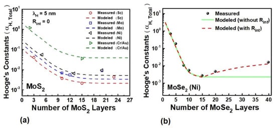
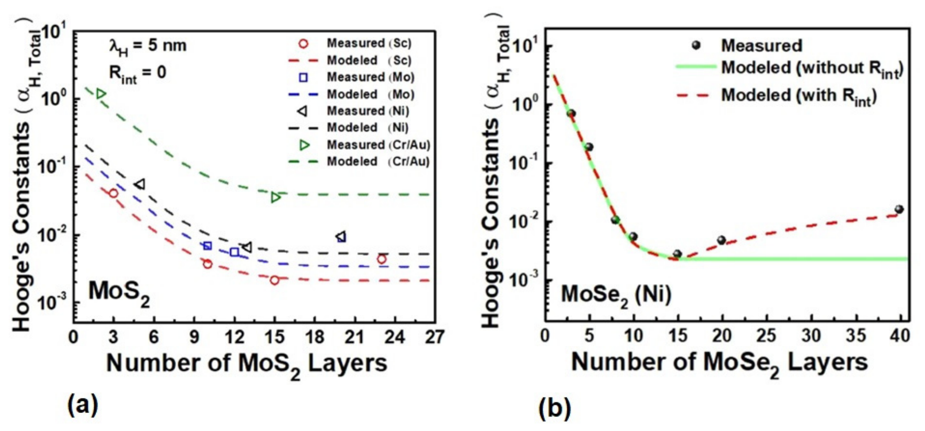
The other interesting direction of noise studies on 2D TMDs is thickness-dependent noise mechanisms. Figure 1 shows the dependence of Hooge constants on the number of layers in MoS2 and MoSe2 systems. As mentioned earlier, the number of layers has a strong influence on the electronic properties of 2D TMD transistors. However, several recent studies have also shown that it affects the 1/f noise mechanism itself [59,63,64,65]. Low-frequency noise and I-V characteristics of multilayer WSe2 with ZrO2 passivation and without passivation have been reported [65]. It was concluded that, after the ZrO2 passivation, the noise level was reduced in the low-current operation regime and volume trap density was also reduced. A model for 1/f noise in MoS2 and in MoSe2 FETs for various contact metals and layer number thicknesses has been proposed [60]. In the study, devices fabricated from bulk MoS2 and MoSe2 were investigated that were mechanically exfoliated (spanning 3 to 142 layers) onto heavily doped Si/SiO2. In comparison to the MoS2 FETs, the Hooge parameter in few-layer MoSe2 FETs was shown to decrease more quickly with increasing layer thickness. In the latest study, it was found that multilayer MoS2 follows Hooge-type mobility fluctuation (MF) rather than McWhorter-type carrier-number fluctuation (CNF)—a qualitative crossover from the monolayer case [63]. In monolayer devices, the noise follows the carrier-number fluctuation (CNF) model. This model includes correlated surface mobility fluctuations. The noise level drops in the subthreshold region but grows in the accumulation region. This happens because the quantum capacitance changes the transconductance efficiency. On the other hand, multilayer devices behave differently. For these thicker layers, the Hooge mobility fluctuation (HMF) model is the main mechanism behind the noise.
Figure 1.
Dependence of Hooge constants on the number of layers in MoS2 (a) and MoSe2 (b) systems. Reproduced from [60], with the permission of AIP Publishing.
8. Noise Spectroscopy as a Probe for Ferroic Transitions: A Case Study of Quaternary Thiophosphate CuInP2S6
Quaternary Thio-(Seleno-)phosphates AIMIIIP2X6 (A = Cu, Ag; M = In, Bi, Cr; X = S, Se) are layered ferroelectric–semiconductors that can be grown as thin plates from a few atomic layers to several microns; interest in them has grown with the demand for integrated piezoelectrics, ferroelectric memories, and nanoscale field-controlled elements, and nanosheets of ~5 layer thickness are increasingly investigated for ferroelectric properties, including room-temperature ferroelectricity in ultrathin CuInP2S6 flakes and size effects in the ferrielectric ordering [66]. The family prototype, CuInP2S6 (CIPS), undergoes a first-order order–disorder transition at 315 K with symmetry lowering C2/c → Cc, driven by the dynamics of two sublattices: ordering of Cu+ and displacement of In3+ from the centrosymmetric position [67]. X-ray diffraction resolves three copper positions (off-center Cu1, split into Cu1u/Cu1d; central octahedral Cu2; interlayer tetrahedral Cu3) whose occupancies evolve from a fully polar sublattice at 153 K (100% Cu1u) through progressive disordering to occupational equalization (47%/47%) at the 318 K transition.
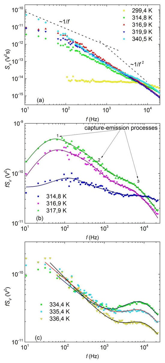
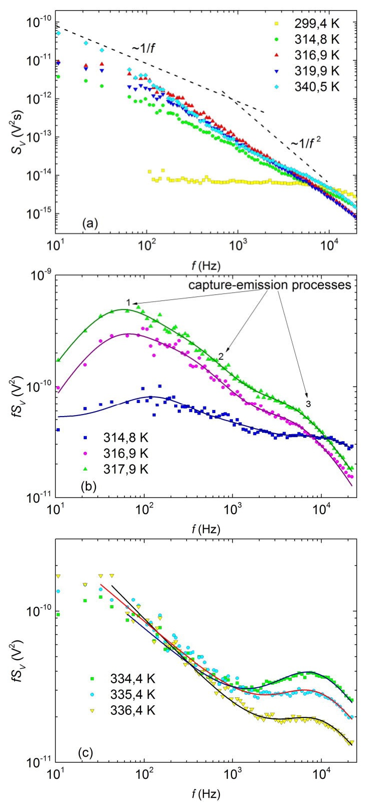
CIPS is the only layered ferroic material ever whose low-frequency noise has been characterized [68,69]. At room temperature (300 K), only the white noise component is visible in the voltage fluctuation spectra; at all measured temperatures above 315 K, the behavior changes qualitatively, the spectra becoming 1/f-type, thereby indicating the phase transition; in the transition vicinity the overall noise level increases and RTN appears, registering jumps between two states of the physical system—a noise type frequently observed in materials of ferroic origin—while the superposition of several RTN components builds the 1/f spectra [68]. Typical noise spectra of CuInP2S6 (CIPS) are shown in Figure 2.
Figure 2.
Voltage fluctuation spectra of CuInP2S6 at some temperatures (a), noise voltage spectral density multiplied by frequency of CuInP2S6 taken at two different temperature ranges: 314–318 K (b) and 334–336 K (c). Reproduced from [68], with the permission of AIP Publishing. The dashed lines in panel (a) indicate the (1/f) and (1/f^2) dependences, and the numbers 1–3 in panel (b) denote individual charge-carrier capture–emission processes.
The decomposition of the noise spectra helped to extract temperature-dependent processes following the Arrhenius law with activation energies of 0.57, 0.74, and 0.10 eV. These were assigned, respectively, to (i) an additional noise source in the ferroelectric regime linked to the phase-transition dynamics; (ii) Cu-ion hopping, since 0.74 eV coincides with the ionic-conductivity activation energy, with a related generation–recombination process (0.68 eV) likewise attributed to copper hopping and its temperature decrease explained by increasing Cu jumps into the interlayer space; and (iii) defect pinning, since 0.10 eV falls within the 3.1 eV forbidden gap of CIPS—consistently corroborated by offset, antisymmetric P–E hysteresis loops attributable to stabilized defects and domain-wall pinning [2]. A single electrical fluctuation measurement thus resolves order-parameter dynamics, the diffusive motion of the very ions whose ordering constitutes the transition, and the pinning landscape of the domain structure.
The broader ferroic noise context remains thin: dielectric-and-noise studies of multiferroic BaTiO3–CoFe2O4 and BaTiO3–NiFe2O4 composites at their phase transitions [70,71], and the application of noise spectroscopy in ferroelectric materials [8] is explicitly recognized as a relatively new area still lacking a framework that correlates noise-spectral processes with material-specific features [2].
9. Random Telegraph Noise in CuScP2S6/MoS2 Heterostructures
CuScP2S6 (CSPS) is a new and still rarely studied material from the Quaternary Thiophosphate family, and not much has been published about it so far. It is a 2D vdW material, built from P2S6 units that are held together by interlayer Cu+ and Sc3+ cations. It is an insulator with a band gap of about 2.2–2.3 eV. Because the material has been studied so little, only one study on low-frequency noise is available [72], which makes CSPS an attractive model platform for studying noise physics. In the context of noise research, the main contribution of this work is the discovery of an unexpected effect: optical excitation can produce “giant” random telegraph noise in large-area CSPS/MoS2 devices. This goes against the usual understanding, in which RTN is seen only as a feature of nanoscale channels, caused by individual charge-trapping events. In large devices, such events are normally averaged out into smooth 1/f noise. Here, in contrast, a small number of light-activated defects inside the insulating thiophosphate control the conductance of an extended channel. This is a mesoscopic regime that, according to the authors, had not been reported before, either in 2D heterostructures or in mesoscopic devices.
At the same time, several limitations and open questions remain. The effect is shown only at sub-ambient temperatures, not at room temperature. Because CSPS itself has been published about so little, broader reproducibility, a deeper understanding of the defect nature, and operation at higher temperatures all remain open topics for future research.
10. Low-Frequency Noise Across Layered Materials: Challenges and Perspectives
Table 1 summarizes the principal low-frequency noise studies discussed in this review, comparing the investigated materials, representative device configurations, dominant physical mechanisms, and current limitations. To facilitate a consistent comparison, we also compiled the noise mechanisms assigned in the original studies on the basis of their experimental analyses. Low-frequency noise measurements are mainly interpreted using analytical and stochastic fluctuation models, particularly the McWhorter-type carrier-number fluctuation (CNF) model and the Hooge-type mobility fluctuation (MF) model. Accordingly, Table 1 seeks to present this information as accurately and consistently as possible by reporting the dominant mechanism assigned in each original study and, where available, the experimental and theoretical basis for that assignment.
Table 1.
Summary of reported low-frequency noise characteristics, proposed mechanisms, and study limitations in selected low-dimensional materials and devices.
As shown in Table 1, mobility fluctuations are identified as the dominant source of low-frequency noise in high-quality graphene devices. Graphene thus represents the first material system in which the dominance of the mobility fluctuation (MF) mechanism was demonstrated directly and conclusively. In contrast, wide-bandgap hBN and most TMD devices are primarily governed by charge trapping and detrapping processes associated with intrinsic defects and interfaces, leading to carrier-number fluctuations (CNF) and random telegraph noise (RTN). However, multilayer TMD devices with improved contacts and reduced interface disorder increasingly exhibit MF-dominated behavior, illustrating that the dominant mechanism evolves with both material quality and device design. Layered van der Waals thiophosphates differ fundamentally from graphene and conventional semiconductor systems because their low-frequency noise is governed not only by defect-related processes but also by collective ferroic phenomena. In CuInP2S6, low-frequency noise directly reflects phase-transition dynamics and Cu-ion motion, whereas CuScP2S6/MoS2 heterostructures exhibit giant RTN associated with photoactivated deep defects. Although these results highlight the unique capabilities of noise spectroscopy in ferroic systems, the available experimental evidence remains scarce, preventing broader generalization.
Overall, the comparison presented in Table 1 demonstrates that low-frequency noise spectroscopy provides a common experimental framework for investigating defect dynamics, transport mechanisms, interface phenomena, and ferroic phase transitions across a wide range of layered materials. At the same time, it reveals several important limitations of the current literature. First, the overwhelming majority of reported studies have been performed on field-effect transistor (FET) devices or related electronic structures. Consequently, the measured fluctuations reflect the response of the complete device rather than the active material alone, and contributions originating from contacts, gate dielectrics, interfaces, encapsulation layers, and fabrication-induced defects often cannot be unambiguously separated from the intrinsic properties of the material itself. Second, the available literature is highly unbalanced. While graphene has reached a relatively mature stage, allowing competing noise mechanisms to be critically evaluated, phosphorus chalcogenides and many other emerging layered materials remain insufficiently explored to establish general trends.
Table 1 suggests that low-frequency noise spectroscopy is currently expected to serve two distinct purposes simultaneously: optimization of electronic device performance and investigation of the microscopic origin of electrical fluctuations. Although these objectives are closely related, pursuing both within the same experiment often complicates the interpretation of the measured noise spectra. In this context, low-frequency noise spectroscopy may provide its greatest value as a complementary characterization technique, used alongside structural, electrical, and spectroscopic methods. Once the device architecture has been optimized and the dominant extrinsic noise sources minimized, low-frequency noise measurements can provide unique insight into intrinsic defect dynamics, charge transport mechanisms, and collective phenomena that are difficult to access by conventional characterization techniques. Future progress will therefore depend not only on extending low-frequency noise studies to new classes of layered materials but also on developing standardized measurement protocols and reporting methodologies that enable meaningful quantitative comparisons between different material systems.
The comparison reveals that no universal microscopic mechanism can account for the observed low-frequency noise across all layered materials. Instead, the relative contributions of CNF and MF, as well as other material-specific fluctuation processes, depend strongly on material quality, carrier concentration, substrate and interface properties, and device architecture. A further promising direction is the integration of LFN spectroscopy with first-principles calculations and atomistic simulations. While LFN measurements provide experimental information on fluctuation kinetics, characteristic time scales, and activation energies, theoretical calculations can relate these signatures to specific defect configurations and composition-dependent changes in electronic structure and lattice dynamics. This approach has already enabled the assignment of substitutional carbon at the boron site as the most likely origin of RTN in hBN [51]. More broadly, DFT studies of sulfur-substituted perovskites demonstrate how anion substitution modifies chemical bonding, band structure, optical response, mechanical stiffness, and thermal transport [73,74]. Although the latter studies do not directly address low-frequency noise, they illustrate the broader potential of first-principles modeling to provide a microscopic framework for interpreting experimental transport and noise measurements. First-principles DFT calculations and nonradiative multiphonon simulations provide an additional microscopic level of analysis by linking experimentally determined activation energies and characteristic time constants to particular atomic defect configurations.
11. Conclusions
This review has surveyed low-frequency noise studies across the principal classes of two-dimensional layered materials, including graphene, hBN, TMDs, and thiophosphates. Collectively, these studies demonstrate that LFN spectroscopy is a sensitive, non-destructive probe of carrier transport, defect dynamics, interfaces, and even collective phase-transition phenomena. However, no universal microscopic mechanism describes all layered materials. Mobility fluctuations have been demonstrated directly as the dominant noise source in high-quality graphene devices, whereas other graphene structures may exhibit carrier-number fluctuations or mixed contributions depending on material quality, substrate, carrier density, and proximity to the Dirac point. Charge trapping and detrapping dominate many hBN and monolayer TMD devices. In layered thiophosphates, LFN additionally probes Cu-ion motion, ferroic ordering, and phase-transition dynamics. Noise spectroscopy can be regarded as a unified, non-destructive probe across the whole 2D family. Unfortunately, no single microscopic mechanism is universal.
Noise can be both suppressed and exploited, and two opposite engineering goals run through this review. On one hand, much work aims to reduce noise—through better material quality, water-free fabrication, high-κ or hBN encapsulation, contact engineering, and even, counterintuitively, controlled electron-beam irradiation, which lowers noise despite adding defects. On the other hand, the most recent work treats noise as a functional resource rather than a defect. Together, these directions show that the field is maturing from simply measuring and minimizing noise toward deliberately controlling and using it.
The research landscape is strongly uneven. Graphene and TMDs have been noise-mapped in great detail, and hBN has been studied thoroughly both as a substrate and as a defect host. By contrast, the ferroelectrically and magnetically ordered phosphorus chalcogenides remain almost untouched: within this family, CuInP2S6 is the only layered ferroic whose low-frequency noise has been characterized, and CuScP2S6 has barely been studied at all.
Finally, although defects are widely regarded as major sources of low-frequency noise, atomistic modeling that directly links specific defect configurations to experimentally observed noise signatures is still rarely applied. Future studies should combine LFN spectroscopy with controlled defect introduction or passivation, complementary structural and optical characterization, and first-principles calculations. The combination of LFN measurements with complementary characterization techniques and, where appropriate, DFT (or any other atomistic modelling) calculations provides a valuable methodological framework applicable beyond 2D materials to a broad range of material systems.
Author Contributions
Writing—original draft preparation, I.Z.; writing—review and editing, A.D.; and J.B. All authors have read and agreed to the published version of the manuscript.
Funding
This research received no external funding.
Data Availability Statement
No new data were created or analyzed in this study.
Conflicts of Interest
The authors declare no conflicts of interest.
Abbreviations
The following abbreviations are used in this manuscript:
| 2D | Two-dimensional |
| TMD | Transition metal dichalcogenide |
| LFN | Low-frequency noise |
| vdW | van der Waals |
| G-R | Generation–recombination |
| BN | Boron nitride |
| hBN | Hexagonal boron nitride |
| cBN | Cubic boron nitride |
| RTN | Random telegraph noise |
| AFM | Atomic force microscopy |
| cAFM | Conductive atomic force microscopy |
| SLG | Single layer graphene |
| BLG | Bilayer graphene |
| MLG | Multiple layer graphene |
| CNF | Carrier-number fluctuations |
| MF | Mobility fluctuations |
| FET | Field-effect transistor |
| ALD | Atomic layer deposition |
| CIPS | CuInP2S6 |
| CSPS | CuScP2S6 |
References
- Johnson, J.B. The Schottky effect in low frequency circuits. Phys. Rev. 1925, 26, 71–85. [Google Scholar] [CrossRef] [Scilit]
- Vandamme, L.K.J. Noise as a Diagnostic Tool for Quality and Reliability of Electronic Devices. IEEE Trans. Electron Devices 1994, 41, 2176–2187. [Google Scholar] [CrossRef] [Scilit]
- Jones, B.K. Low-Frequency Noise Spectroscopy. IEEE Trans. Electron Devices 1994, 41, 5169–5173. [Google Scholar] [CrossRef] [Scilit]
- Van der Ziel, A.; Chenette, E.R. Noise in solid state devices. In Advances in Electronics and Electron Physics; Academic Press: New York, NY, USA, 1978; Volume 46, pp. 313–383. [Google Scholar]
- Dutta, P.; Horn, P.M. Low-frequency fluctuations in solids: 1/f noise. Rev. Mod. Phys. 1981, 53, 497–516. [Google Scholar] [CrossRef] [Scilit]
- Weissman, M.B. 1/f noise and other slow, nonexponential kinetics in condensed matter. Rev. Mod. Phys. 1988, 60, 537–571. [Google Scholar] [CrossRef] [Scilit]
- Wong, H. Low-frequency noise study in electron devices: Review and update. Microelectron. Reliab. 2003, 43, 585–599. [Google Scholar] [CrossRef] [Scilit]
- Raychaudhuri, A.K. Measurement of 1/f noise and its application in materials science. Curr. Opin. Solid State Mater. Sci. 2002, 6, 67–85. [Google Scholar] [CrossRef] [Scilit]
- Balandin, A.A. Low-frequency 1/f noise in graphene devices. Nat. Nanotechnol. 2013, 8, 549–555. [Google Scholar] [CrossRef] [Scilit] [PubMed]
- Karnatak, P.; Paul, T.; Islam, S.; Ghosh, A. 1/f noise in van der Waals materials and hybrids. Adv. Phys. X 2017, 2, 428–449. [Google Scholar] [CrossRef] [Scilit]
- Rao, C.N.R.; Sood, A.K. (Eds.) Graphene: Synthesis, Properties, and Phenomena; John Wiley & Sons: Hoboken, NJ, USA, 2013. [Google Scholar]
- Halevi, G.; Moed, H.F. 10 years of research impact: Top cited papers in Scopus 2001–2011. Res. Trends 2014, 1, 2. [Google Scholar]
- Plume, A. Graphene: Ten years of the ‘gold rush’. Res. Trends 2014, 1, 4. [Google Scholar]
- Weis, J.E.; Charpentier, S.; Kempinska, A. Graphene Research and Advances: Report December 2019; SIO Grafen: Gothenburg, Sweden, 2019; Available online: https://siografen.se/app/uploads/2020/01/Research_Intelligence_2019-2-.pdf (accessed on 3 August 2026).
- Novoselov, K.S.; Geim, A.K.; Morozov, S.V.; Jiang, D.; Zhang, Y.; Dubonos, S.V.; Grigorieva, I.V.; Firsov, A.A. Electric field effect in atomically thin carbon films. Science 2004, 306, 666–669. [Google Scholar] [CrossRef] [Scilit] [PubMed]
- Geim, A.K.; Novoselov, K.S. The rise of graphene. Nat. Mater. 2007, 6, 183–191. [Google Scholar] [CrossRef] [Scilit] [PubMed]
- Lin, Y.M.; Avouris, P. Strong suppression of electrical noise in bilayer graphene nanodevices. Nano Lett. 2008, 8, 2119–2125. [Google Scholar] [CrossRef] [Scilit] [PubMed]
- Pellegrini, B. 1/f noise in graphene. Eur. Phys. J. B 2013, 86, 373. [Google Scholar] [CrossRef] [Scilit]
- Macucci, M.; Marconcini, P. Theoretical Comparison between the Flicker Noise Behavior of Graphene and of Ordinary Semiconductors. J. Sens. 2020, 1, 2850268. [Google Scholar]
- Liu, G.; Rumyantsev, S.; Shur, M.S.; Balandin, A.A. Origin of 1/f noise in graphene multilayers: Surface vs. volume. Appl. Phys. Lett. 2013, 102, 093111. [Google Scholar] [CrossRef] [Scilit]
- Rehman, A.; Delgado Notario, J.A.; Salvador Sanchez, J.; Meziani, Y.M.; Cywiński, G.; Knap, W.; Balandin, A.A.; Levinshtein, M.; Rumyantsev, S. Nature of the 1/f noise in graphene-direct evidence for the mobility fluctuation mechanism. Nanoscale 2022, 14, 7242–7249. [Google Scholar] [CrossRef] [Scilit] [PubMed]
- Kalmbach, C.C.; Ahlers, F.J.; Schurr, J.; Müller, A.; Feilhauer, J.; Kruskopf, M.; Pierz, K.; Haug, R.J. Nonequilibrium mesoscopic conductance fluctuations as the origin of 1/f noise in epitaxial graphene. Phys. Rev. B 2016, 94, 205430. [Google Scholar] [CrossRef] [Scilit]
- Kamada, M.; Zeng, W.; Laitinen, A.; Sarkar, J.; Yeh, S.S.; Tappura, K.; Seppä, H.; Hakonen, P. Suppression of 1/f noise in graphene due to anisotropic mobility fluctuations induced by impurity motion. Commun. Phys. 2023, 6, 207. [Google Scholar] [CrossRef] [Scilit]
- Pellegrino, F.M.; Falci, G.; Paladino, E. 1/f critical current noise in short ballistic graphene Josephson junctions. Commun. Phys. 2020, 3, 6. [Google Scholar] [CrossRef] [Scilit]
- Hossain, Z.; Rumyantsev, S.; Shur, M.S.; Balandin, A.A. Reduction of 1/f noise in graphene after electron-beam irradiation. Appl. Phys. Lett. 2013, 102, 153512. [Google Scholar] [CrossRef] [Scilit]
- Arnold, H.N.; Sangwan, V.K.; Schmucker, S.W.; Cress, C.D.; Luck, K.A.; Friedman, A.L.; Campbell, P.M.; Hersam, M.C. Reducing flicker noise in chemical vapor deposition graphene field-effect transistors. Appl. Phys. Lett. 2016, 108, 073105. [Google Scholar] [CrossRef] [Scilit]
- Dean, C.R.; Young, A.F.; Meric, I.; Lee, C.; Wang, L.; Sorgenfrei, S.; Watanabe, K.; Taniguchi, T.; Kim, P.; Shepard, K.L.; et al. Boron nitride substrates for high-quality graphene electronics. Nat. Nanotechnol. 2010, 5, 722–726. [Google Scholar] [CrossRef] [Scilit] [PubMed]
- Wang, L.; Meric, I.; Huang, P.Y.; Gao, Q.; Gao, Y.; Tran, H.; Taniguchi, T.; Watanabe, K.; Campos, L.M.; Muller, D.A.; et al. One-dimensional electrical contact to a two-dimensional material. Science 2013, 342, 614–617. [Google Scholar] [CrossRef] [Scilit] [PubMed]
- Geim, A.K.; Grigorieva, I.V. Van der Waals heterostructures. Nature 2013, 499, 419–425. [Google Scholar] [CrossRef] [Scilit] [PubMed]
- Li, X.; Lu, X.; Li, T.; Yang, W.; Fang, J.; Zhang, G.; Wu, Y. Noise in graphene superlattices grown on hexagonal boron nitride. ACS Nano 2015, 9, 11382–11388. [Google Scholar] [CrossRef] [Scilit] [PubMed]
- Kayyalha, M.; Chen, Y.P. Observation of reduced 1/f noise in graphene field effect transistors on boron nitride substrates. Appl. Phys. Lett. 2015, 107, 113101. [Google Scholar] [CrossRef] [Scilit]
- Kumar, C.; Kuiri, M.; Jung, J.; Das, T.; Das, A. Tunability of 1/f noise at multiple Dirac cones in hBN encapsulated graphene devices. Nano Lett. 2016, 16, 1042–1049. [Google Scholar] [CrossRef] [Scilit] [PubMed]
- Ranjan, A.; Puglisi, F.M.; Raghavan, N.; O’SHea, S.J.; Shubhakar, K.; Pavan, P.; Padovani, A.; Larcher, L.; Pey, K.L. Random telegraph noise in 2D hexagonal boron nitride dielectric films. Appl. Phys. Lett. 2018, 112, 133103. [Google Scholar] [CrossRef] [Scilit]
- Kim, L.H.; Kim, K.; Park, S.; Jeong, Y.J.; Kim, H.; Chung, D.S.; Kim, S.H.; Park, C.E. Al2O3/TiO2 nanolaminate thin film encapsulation for organic thin film transistors via plasma-enhanced atomic layer deposition. ACS Appl. Mater. Interfaces 2014, 6, 6731–6738. [Google Scholar] [CrossRef] [Scilit] [PubMed]
- Wang, Y.; Ho, V.X.; Henschel, Z.N.; Cooney, M.P.; Vinh, N.Q. Effect of high-κ dielectric layer on 1/f noise behavior in graphene field-effect transistors. ACS Appl. Nano Mater. 2021, 4, 3647–3653. [Google Scholar] [CrossRef] [Scilit]
- Tian, M.; Hu, Q.; Gu, C.; Xiong, X.; Zhang, Z.; Li, X.; Wu, Y. Tunable 1/f noise in CVD Bernal-stacked bilayer graphene transistors. ACS Appl. Mater. Interfaces 2020, 12, 17686–17690. [Google Scholar] [CrossRef] [Scilit] [PubMed]
- Tran, N.A.M.; Fakih, I.; Durnan, O.; Hu, A.; Aygar, A.M.; Napal, I.; Centeno, A.; Zurutuza, A.; Szkopek, T. Graphene field effect transistor scaling for ultra-low-noise sensors. Nanotechnology 2021, 32, 045502. [Google Scholar] [CrossRef] [Scilit] [PubMed]
- Nah, J.; Perkins, F.K.; Lock, E.H.; Nath, A.; Boyd, A.; Myers-Ward, R.L.; Gaskill, D.K.; Osofsky, M.; Rao, M.V. Electrical and low frequency noise characterization of graphene chemical sensor devices having different geometries. Sensors 2022, 22, 1183. [Google Scholar] [CrossRef] [Scilit] [PubMed]
- Shetty, N.; Chianese, F.; He, H.; Huhtasaari, J.; Ghasemi, S.; Moth-Poulsen, K.; Kubatkin, S.; Bauch, T.; Lara-Avila, S. Ultralow 1/f noise in epigraphene devices. Appl. Phys. Lett. 2024, 124, 093503. [Google Scholar] [CrossRef] [Scilit]
- Glemža, J.; Pliaterytė, I.; Matukas, J.; Gudaitis, R.; Vasiliauskas, A.; Jankauskas, Š.; Meškinis, Š. Low-frequency noise characteristics of graphene/h-BN/Si junctions. Crystals 2025, 15, 747. [Google Scholar] [CrossRef] [Scilit]
- Mireckas, F.; Meisak, D.; Pralgauskaitė, S.; Macutkevič, J.; Matukas, J.; Banys, J. Low-Frequency Noise and Resistivity of Hybrid MWCNT/Ni@C/EPOXY Composites. Fluct. Noise Lett. 2025, 24, 2540018. [Google Scholar] [CrossRef] [Scilit]
- Mireckas, F.; Pralgauskaitė, S.; Korzhenevskaya, M.; Matukas, J.; Plyushch, A.; Banys, J.; Platnieks, O.; Barkane, A.; Gaidukovs, S. Dielectric, low-frequency noise and mechanical properties of hybrid carbon nanotubes/graphene nanoplatelets epoxy composites. Polym. Compos. 2025, 46, 3153–3164. [Google Scholar] [CrossRef] [Scilit]
- Tretjak, M.; Pralgauskaitė, S.; Matukas, J.; Plyushch, A.; Macutkevič, J.; Banys, J.; Ivanov, M.; Fierro, V.; Celzard, A. Electrical Resistivity and Microwave Properties of Carbon Fiber Felt Composites. Materials 2022, 15, 8654. [Google Scholar] [CrossRef] [Scilit] [PubMed]
- Glemža, J.; Palenskis, V.; Gudaitis, R.; Jankauskas, Š.; Guobienė, A.; Vasiliauskas, A.; Tamulevičienė, A.; Meškinis, Š.; Matukas, J. Low-frequency noise of directly synthesized graphene/Si (100) junction. Diam. Relat. Mater. 2022, 127, 109207. [Google Scholar] [CrossRef] [Scilit]
- Tretjak, M.; Pralgauskaitė, S.; Matukas, J.; Macutkevič, J.; Banys, J.; Shenderova, O. Low frequency noise and resistivity characteristics of hybrid composites with onion-like carbon and multi-walled carbon nanotubes. Fluct. Noise Lett. 2019, 18, 1940009. [Google Scholar] [CrossRef] [Scilit]
- Kim, K.K.; Hsu, A.; Jia, X.; Kim, S.M.; Shi, Y.; Hofmann, M.; Nezich, D.; Reina, A.; Dresselhaus, M.; Palacios, T.; et al. Synthesis and characterization of hexagonal boron nitride film as a dielectric layer for graphene devices. ACS Nano 2012, 6, 8583–8590. [Google Scholar] [CrossRef] [Scilit] [PubMed]
- Gupta, A.; Sakthivel, T.; Seal, S. Recent development in 2D materials beyond graphene. Prog. Mater. Sci. 2015, 73, 44–126. [Google Scholar] [CrossRef] [Scilit]
- Martini, L.; Miseikis, V.; Esteban, D.; Azpeitia, J.; Pezzini, S.; Paletti, P.; Ochapski, M.W.; Convertino, M.; Garcia Hernandez, M.; Jimenez, I.; et al. Scalable high-mobility graphene/hBN heterostructures. ACS Appl. Mater. Interfaces 2023, 15, 37794–37801. [Google Scholar] [CrossRef] [Scilit] [PubMed]
- Shtansky, D.V.; Matveev, A.T.; Permyakova, E.S.; Leybo, D.V.; Konopatsky, A.S.; Sorokin, P.B. Recent progress in fabrication and application of BN nanostructures and BN-based nanohybrids. Nanomaterials 2022, 12, 2810. [Google Scholar] [CrossRef] [Scilit] [PubMed]
- Yankowitz, M.; Ma, Q.; Jarillo-Herrero, P.; LeRoy, B.J. van der Waals heterostructures combining graphene and hexagonal boron nitride. Nat. Rev. Phys. 2019, 1, 112–125. [Google Scholar] [CrossRef] [Scilit]
- Stolyarov, M.A.; Liu, G.; Rumyantsev, S.L.; Shur, M.; Balandin, A.A. Suppression of 1/f noise in near-ballistic h-BN-graphene-h-BN heterostructure field-effect transistors. Appl. Phys. Lett. 2015, 107, 023106. [Google Scholar] [CrossRef] [Scilit]
- Huang, Z.; Lee, R.G.; Cuniberto, E.; Song, J.; Lee, J.; Alharbi, A.; Taniguchi, T.; Watanabe, K.; Shahrjerdi, D. Characterizing defects inside hexagonal boron nitride using random telegraph signals in van der Waals 2D transistors. ACS Nano 2024, 18, 28700–28711. [Google Scholar] [CrossRef] [Scilit] [PubMed]
- Li, S.; Gali, A. Bistable carbon-vacancy defects in h-BN. Front. Quantum Sci. Technol. 2022, 1, 1007756. [Google Scholar] [CrossRef] [Scilit]
- Mukherjee, S.; Samanta, G.; Moulick, S.; Kulkarni, R.; Watanabe, K.; Taniguchi, T.; Majumdar, K.; Saha, S.; Pal, A.N. Single-defect spectroscopy via random telegraph noise in graphene contacted ReS2-hBN heterostructures. Phys. Rev. B 2026, 113, L201402. [Google Scholar] [CrossRef] [Scilit]
- Ataca, C.; Sahin, H.; Ciraci, S. Stable, single-layer MX2 transition-metal oxides and dichalcogenides in a honeycomb-like structure. J. Phys. Chem. C 2012, 116, 8983–8999. [Google Scholar] [CrossRef] [Scilit]
- Strachan, J.; Masters, A.F.; Maschmeyer, T. 3R-MoS2 in Review: History, Status, and Outlook. ACS Appl. Energy Mater. 2021, 4, 7405–7418. [Google Scholar] [CrossRef] [Scilit]
- Jones, L.A.; Xing, Z.; Swallow, J.E.; Shiel, H.; Featherstone, T.J.; Smiles, M.J.; Thomas, P.; Lee, H.; Cheetham, K.J.; Warren, M.R.; et al. Band alignments, electronic structure, and core-level spectra of bulk molybdenum dichalcogenides (MoS2, MoSe2, and MoTe2). J. Phys. Chem. C 2022, 126, 21022–21033. [Google Scholar] [CrossRef] [Scilit] [PubMed]
- Sangwan, V.K.; Arnold, H.N.; Jariwala, D.; Marks, T.J.; Lauhon, L.J.; Hersam, M.C. Low-frequency electronic noise in single-layer MoS2 transistors. Nano Lett. 2013, 13, 4351–4355. [Google Scholar] [CrossRef] [Scilit] [PubMed]
- Wang, J.W.; Liu, Y.P.; Chen, P.H.; Chuang, M.H.; Pezeshki, A.; Chang, S.E.; Huang, P.Y.; Lin, J.H.; Ling, D.C.; Chiu, P.W.; et al. Controlled Low-Frequency Electrical Noise of Monolayer MoS2 with Ohmic Contact and Tunable Carrier Concentration. Adv. Electron. Mater. 2018, 4, 1700340. [Google Scholar] [CrossRef] [Scilit]
- Kwon, J.; Delker, C.J.; Harris, C.T.; Das, S.R.; Janes, D.B. Experimental and modeling study of 1/f noise in multilayer MoS2 and MoSe2 field-effect transistors. J. Appl. Phys. 2020, 128, 094304. [Google Scholar] [CrossRef] [Scilit]
- Zhang, B.; Hu, C.; Xin, Y.; Li, Y.; Xie, Y.; Xing, Q.; Zhang, D.; Zhou, H.; Wang, C. Analysis of low-frequency 1/f noise characteristics for MoTe2 ambipolar field-effect transistors. Nanomaterials 2022, 12, 1325. [Google Scholar] [CrossRef] [Scilit] [PubMed]
- Kang, W.M.; Cho, I.T.; Roh, J.; Lee, C.; Lee, J.H. Low-Frequency Noise Characteristics in Multi-Layer WSe2 Field Effect Transistors with Different Contact Metals. J. Nanosci. Nanotechnol. 2019, 19, 6422–6428. [Google Scholar] [CrossRef] [Scilit] [PubMed]
- Chen, L.; Lu, Z.; Song, Y.; Guo, R.; Li, H.; Raskin, J.P.; Flandre, D.; Liu, Y.; Liao, L.; Li, G. Quantum capacitance impact on low-frequency noise in MoS2 transistors. Phys. Rev. Appl. 2025, 23, 054012. [Google Scholar] [CrossRef] [Scilit]
- Manjula, M.M.; Ramesh, R. Low-frequency noise performance of a molybdenum ditelluride double-gate MOSFET. J. Comput. Electron. 2023, 22, 1433–1442. [Google Scholar] [CrossRef] [Scilit]
- Ko, S.P.; Piao, M.; Jang, H.K.; Shin, J.M.; Jin, J.E.; Kim, D.H.; Kim, S.; Lee, G.T.; Cho, J. Low frequency noise reduction in multilayer WSe2 field effect transistors. In Proceedings of the 2015 IEEE 15th International Conference on Nanotechnology (IEEE-NANO), Rome, Italy, 27–30 July 2015; pp. 1118–1121. [Google Scholar]
- Belianinov, A.; He, Q.; Dziaugys, A.; Maksymovych, P.; Eliseev, E.; Borisevich, A.; Morozovska, A.; Banys, J.; Vysochanskii, Y.; Kalinin, S.V. CuInP2S6 room temperature layered ferroelectric. Nano Lett. 2015, 15, 3808–3814. [Google Scholar] [CrossRef] [Scilit] [PubMed]
- Maisonneuve, V.; Cajipe, V.B.; Simon, A.; Von Der Muhll, R.; Ravez, J. Ferrielectric ordering in lamellar CuInP2S6. Phys. Rev. B 1997, 56, 10860–10864. [Google Scholar] [CrossRef] [Scilit]
- Zamaraite, I.; Matukas, J.; Pralgauskaite, S.; Vysochanskii, Y.; Banys, J.; Dziaugys, A. Low-frequency noise characteristics of lamellar ferrielectric crystal CuInP2S6 at the phase transition. J. Appl. Phys. 2017, 122, 024101. [Google Scholar] [CrossRef] [Scilit]
- Banys, J.; Dziaugys, A.; Glukhov, K.E.; Morozovska, A.N.; Morozovsky, N.V.; Vysochanskii, Y.M. Van der Waals Ferroelectrics: Properties and Device Applications of Phosphorous Chalcogenides; John Wiley & Sons: Hoboken, NJ, USA, 2022. [Google Scholar]
- Pralgauskaitė, S.; Matukas, J.; Grigalaitis, R.; Banys, J.; Zamaraitė, I.; Petrović, M.V.; Bobić, J.D.; Vijatović Petrović, M.M.; Džunuzović, A.S.; Stojanović, B.D. Low frequency noise characteristics of BaTiO3–NiFe2O4 composites at phase transition. In Proceedings of the 2015 International Conference on Noise and Fluctuations (ICNF), Xi’an, China, 2–6 June 2015; pp. 1–4. [Google Scholar]
- Banys, J.; Ramoška, T.; Matukas, J.; Pralgauskaitė, S.; Alawneh, F.M.M.; Shvartsman, V.V.; Lupascu, D.C. Investigation of dielectric and noise properties of the multiferoic composite BaTiO3 with CoFe2O4. Ferroelectrics 2011, 417, 25–32. [Google Scholar] [CrossRef] [Scilit]
- Ghosh, A.; Sen, D.; Ray, S.; Nair, R.T.; Rasyotra, A.; Gusmao, R.; Sofer, Z.; Das, S. Light-induced giant random telegraph noise in CuScP2S6/MoS2 heterostructures and their use in noise resilience image inference. Nat. Commun. 2026, 17, 5297. [Google Scholar] [CrossRef] [Scilit] [PubMed]
- Szeleszczuk, Ł.; Mądra-Gackowska, K.; Gackowski, M. Exploring the effects of oxygen replacement by sulfur in SrTiO3: A comprehensive DFT investigation. J. Phys. Chem. Solids 2026, 213, 113575. [Google Scholar] [CrossRef] [Scilit]
- Szeleszczuk, Ł.; Mądra-Gackowska, K.; Gackowski, M. From oxide to sulfide: Computational design of NaTaO3−xSx perovskites with tailored electronic and thermal behavior. Vacuum 2026, 248, 115212. [Google Scholar] [CrossRef] [Scilit]

Disclaimer/Publisher’s Note: The statements, opinions and data contained in all publications are solely those of the individual author(s) and contributor(s) and not of MDPI and/or the editor(s). MDPI and/or the editor(s) disclaim responsibility for any injury to people or property resulting from any ideas, methods, instructions or products referred to in the content. |
© 2026 by the authors. Licensee MDPI, Basel, Switzerland. This article is an open access article distributed under the terms and conditions of the Creative Commons Attribution (CC BY) license.