


Abstract
The morphology of CVD-grown molybdenum disulfide (MoS2) is sensitive to the local precursor environment, which governs nucleation density, edge stability, and growth kinetics. In this work, we systematically investigate the effect of precursor ratio on the morphological evolution of MoS2 microstructures synthesized by atmospheric-pressure chemical vapor deposition on SiO2/Si substrates. By varying the relative amounts of MoO3 and sulfur precursors, distinct growth regimes were obtained, ranging from compact hexagonal and quasi-circular domains to multilayer hexagonal structures, triangular domains, and dendritic morphologies. At higher MoO3 loading, growth is dominated by dense nucleation, leading to isolated few-layer hexagonal domains. A moderate reduction in Mo precursor concentration promotes diffusion-assisted growth and secondary nucleation, resulting in multilayer hexagonal structures with aligned or slightly rotated stacked layers. Under sulfur-rich conditions, morphology evolves into triangular domains due to anisotropic edge stabilization, while further increase in sulfur concentration gives rise to branched dendritic structures through kinetically limited, diffusion-dominated growth. Cross-sectional FIB analysis reveals dense vertical stacking and lateral displacement of upper layers in the multilayer hexagonal domains. Raman and photoluminescence measurements confirm strong correlations between morphology, layer thickness, and optical response, with thinner regions exhibiting reduced Raman peak separation, enhanced photoluminescence intensity, and blue-shifted excitonic transitions. The results show that, under fixed APCVD reactor geometry, source positions, temperature profile, carrier-gas flow, and nominal growth duration, the nominal MoO3 to sulfur source-loading ratio reproducibly correlates with the transition between compact hexagonal, multilayer hexagonal, triangular, and dendritic MoS2 morphologies on amorphous SiO2/Si substrates. Because vapor-phase Mo- and S-containing partial pressures were not directly measured, this ratio is treated as a nominal source-inventory descriptor rather than as a direct vapor-phase stoichiometric ratio. The observed trends are interpreted using a qualitative thermodynamic and kinetic framework based on precursor fluence, nucleation density, edge stability, and diffusion-limited growth.
1. Introduction
The controlled synthesis of two-dimensional transition metal dichalcogenides (TMDs), particularly molybdenum disulfide (MoS2), has attracted significant attention due to their unique structural, electronic, and optoelectronic properties [1,2]. Among the various synthesis techniques, chemical vapor deposition (CVD) has emerged as a versatile and scalable method for the growth of MoS2 with tunable morphology and layer thickness [3,4]. A critical parameter governing the CVD growth process is the precursor concentration, which directly influences the local chemical environment, supersaturation, and growth kinetics at the substrate surface. Singh et al. demonstrated that the local precursor concentration boundary layer plays a decisive role in controlling MoS2 layer number and domain quality in CVD growth, highlighting that even small variations in effective precursor flux at the substrate surface produce significant changes in the resulting microstructure [5].
Manipulation of precursor concentrations enables control over the morphology and structural characteristics of MoS2, thereby determining its physical and chemical properties [6,7]. Variations in the effective Mo-to-S precursor ratio can lead to the formation of diverse microstructures, including triangular [6,8], hexagonal [6,7], truncated triangular [9], and dendritic domains [10]. These morphological transitions are closely associated with changes in vapor-phase composition and the resulting anisotropic edge growth dynamics [11,12]. Mouloua et al. further showed that distinct MoS2 morphologies are obtained as a direct function of substrate position within the CVD tube furnace, confirming that local precursor concentration gradients are a primary determinant of the final growth morphology [13].
Previous studies have demonstrated that the domain shape of MoS2 is highly sensitive to the Mo-to-S ratio. Wang et al. reported that variations in precursor ratio (Mo to S > 2, ≈1:2, and <2) significantly alter the edge growth kinetics, leading to systematic transformations in crystal morphology [6]. Similarly, Zhu et al. showed that tuning the effective precursor ratio allows for control over surface morphology, crystalline quality, and photoluminescence properties of MoS2 [7]. In sulfur-rich environments, large-area monolayer MoS2 with well-defined triangular domains and sharp edges is typically favored due to enhanced lateral growth and anisotropic S-edge stabilization [14,15]. Van der Zande et al. further demonstrated that grain boundaries and domain morphology in CVD-grown MoS2 are intimately linked to local growth kinetics and precursor availability during nucleation [4].
Furthermore, Özden et al. [9] highlighted the importance of vapor confinement and transport in determining the local Mo and S concentrations near the substrate, emphasizing that the effective Mo-to-S vapor ratio in the growth zone plays a decisive role in controlling domain size, shape, and uniformity. Under controlled sulfur conditions, increasing Mo concentration has been shown to induce a sequence of morphological transitions, where MoS2 domains evolve from triangular to hexagonal, and then become truncated triangular, and eventually revert to triangular shapes due to changes in edge stability and growth kinetics [12]. Complementary theoretical insight was provided by Cao et al., who demonstrated that the equilibrium shape and edge configuration of monolayer MoS2 are strongly controlled by the chemical potentials of Mo and S species [11]. Using density functional theory and Wulff construction analysis, they predicted a morphology evolution from dodecagonal or mixed-edge structures under Mo-rich conditions to hexagonal domains at intermediate chemical potential, and finally to triangular domains under S-rich conditions [11,14]. Moreover, previous experimental studies have shown that the morphology of MoS2 domains is highly sensitive to the relative Mo and S supply [14]. Xu et al. reported that triangular, near-hexagonal, and truncated-triangular MoS2 flakes can be synthesized on SiO2/Si substrates by CVD and proposed that the final domain shape is determined by the relative growth rates of Mo-terminated and S-terminated edges under different sulfur environments [8]. Under strongly sulfur-rich and high-flux conditions, the growth front becomes susceptible to diffusion-limited instabilities, where preferential attachment of adatoms at protruding edge sites promotes branching and the formation of dendritic morphologies rather than compact polygonal domains [10,16].
Despite these advances, a comprehensive understanding of how precursor concentration governs the full spectrum of MoS2 morphological evolution—from compact hexagonal and multilayer stacked domains through triangular to highly branched dendritic structures—as a continuous function of the Mo to S ratio on amorphous SiO2/Si substrates remains incomplete. Existing studies have typically examined one or two morphological regimes in isolation, without establishing a mechanistic framework that connects all transitions within a single experimental series under otherwise fixed growth conditions [5,6,9,13]. Furthermore, the cross-sectional microstructure of multilayer hexagonal domains, including the lateral displacement mechanism of successive stacked layers, has not been directly characterized by FIB analysis and correlated with growth kinetics. Similarly, the spatial evolution of Raman and photoluminescence signatures across structurally complex dendritic domains, and its interpretation in terms of thickness-dependent electron–phonon coupling and trion/exciton balance, has not previously been reported for this morphological regime. In this work, we systematically investigate the morphology of CVD-grown MoS2 microstructures across five distinct nominal precursor-loading conditions and correlate the observed structural and optical properties with the resulting growth regimes. The term “nominal precursor-loading ratio” is used throughout to describe the initially loaded MoO3 and sulfur source inventory under a fixed APCVD reactor geometry, source placement, temperature program, carrier-gas flow, and growth duration. It is not used as a direct measure of vapor-phase Mo:S partial-pressure ratio at the substrate. The morphology sequence is therefore interpreted as a reactor-specific correlation between nominal source inventory, precursor fluence, nucleation density, edge stability, and diffusion-limited growth, rather than as a universal morphology map based only on loaded precursor masses.
2. Materials and Methods
2.1. Growth Method
For the growth of MoS2 thin films, vapor-phase reactions of MoO3 and sulfur (S) precursors were employed. The process was performed in a 1.2 m long clear fused quartz tube (inner diameter 4.6 cm, outer diameter 5 cm, (Raesch Quarz GmbH, Ilmenau, Germany). Silicon substrates (1 × 1 cm) with 90 nm SiO2 were initially cleaned sequentially in acetone, isopropanol, and deionized water for 10 min each, and then subsequently dried under nitrogen gas. The cleaned substrates were then positioned at the center of the furnace within the quartz tube.
A ceramic boat containing MoO3 powder (99%, Sigma-Aldrich Chemie GmbH, Taufkirchen, Germany), was placed at the center of the quartz tube, 40 cm from the inlet. To systematically investigate the effect of precursor ratio on MoS2 morphology, the MoO3 mass varied between 10 mg and 500 mg. The sulfur source (99%, Sigma-Aldrich Chemie GmbH, Taufkirchen, Germany), with mass varied between 200 mg and 400 mg, was positioned 27 cm upstream from the inlet in a lower-temperature zone maintained at 240 °C throughout the growth process. The resulting nominal atomic Mo:S source-loading ratios are summarized in Table S1. These ratios were calculated from the initially loaded MoO3 and sulfur masses and describe the source inventory before the growth process. They are not equivalent to directly measured vapor-phase Mo:S partial-pressure ratios in the reaction zone. To clarify the limiting vapor-pressure and source-depletion scales associated with these source inventories, equilibrium vapor-pressure ceilings and lower-bound depletion times for MoO3 and sulfur are estimated in Supplementary Note S1 and Table S2.
Prior to growth, the furnace was purged with 500 sccm N2 for one hour. The furnace temperature was then ramped to 850 °C at a linear rate of 28 °C min−1 under a continuous N2 flow of 1000 sccm. Upon reaching 850 °C, the peak temperature was maintained for growth durations ranging from 10 to 30 min. However, all morphological characterization results reported in this work were obtained at a fixed growth duration of 10 min, with the MoO3-to-sulfur precursor mass ratio as the sole independently varied parameter across the five growth conditions investigated. Time-series SEM observations at fixed precursor conditions (MoO3 = 10 mg; S = 300 mg) for growth durations of 10–30 min, presented in Figure S1, confirm that the fundamental morphological character is established at 10 min and does not change with increasing growth duration, directly validating the decoupling of growth time and precursor ratio effects. All temperatures were monitored using calibrated thermocouples. Following the growth period, the system was cooled naturally to ambient temperature under a continued N2 flow of 500 sccm at atmospheric pressure. The complete CVD temperature profile and N2 flow rate evolution throughout the process are shown in Figure S2 of the supporting information.
2.2. Characterization of Synthesized Vertical MoS2 Nanosheet
The surface morphology and topographical details of the different MoS2 morphologies were carried out using scanning electron microscopy (SEM; RAITH 150, Raith GmbH, Dortmund, Germany) and atomic force microscopy (AFM; Dimension V, Veeco Instruments GmbH, Aschheim, Germany). All cross-sectional and structural analyses were performed using a FIB Nanoanalytics Auriga 60 dual-beam system (Carl Zeiss AG, Oberkochen, Germany) to analyze the inner morphology of distinct structures. Before cutting, protective carbon and platinum layers were deposited sequentially via an electron beam and a gallium ion beam, respectively. Furthermore, we investigated the material properties with Raman spectroscopy and photoluminescence (PL). The Raman and PL spectra were obtained using a WiTec Alpha 300 confocal Raman microscope (WiTec GmbH, Ulm, Germany). X-ray diffraction (XRD) measurements were performed on a Siemens D5000 diffractometer (Siemens AG, Munich, Germany) using a copper anode and radiation with a wavelength of 0.15406 nm (Cu Kα1) in Bragg–Brentano mode.
3. Results and Discussion
3.1. Precursor Concentration-Dependent Morphological Evolution and Grain Growth in CVD-Grown MoS2
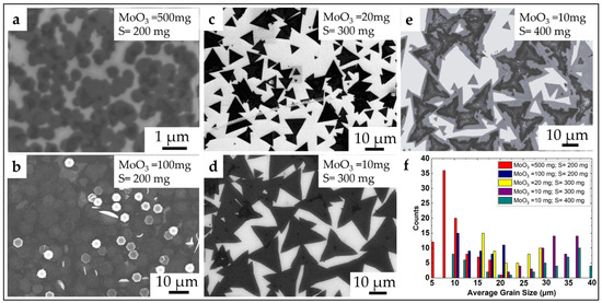
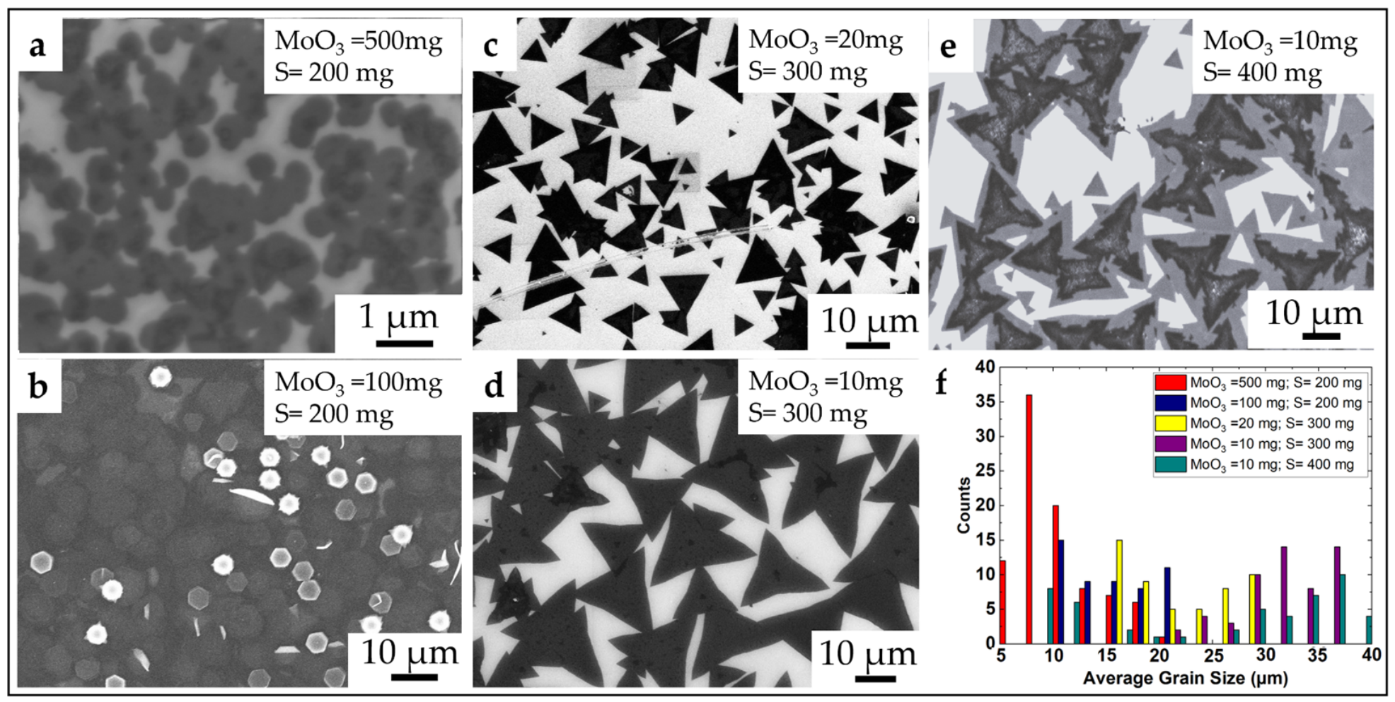
Figure 1 shows the SEM images revealing a systematic evolution of MoS2 morphology with varying MoO3 and sulfur precursor concentrations. As shown in Figure 1a,b, at higher MoO3 loadings (500 mg and 100 mg with 200 mg S), the surface is populated by compact hexagonal and quasi-circular multilayer domains. Moreover, as shown in Figure 1b, the hexagonal multilayer MoS2 structures exhibit two distinct stacking morphologies. In some cases, the additional layers grow directly above the base layer while preserving the lateral orientation and crystallographic alignment, indicating a relatively ordered stacking process. In other cases, the upper layers are slightly rotated with respect to the base layer, producing a star-like morphology. However, such multilayer stacking is not evident in Figure 1a, where the higher MoO3 concentration (500 mg) mainly results in scattered few-layer hexagonal and quasi-circular MoS2 domains with Raman peak separations consistent with mono-to-few-layer thickness (Figure S3). The observed morphological evolution can be understood through the combined influence of local supersaturation, chemical potential, and edge energetics [17]. However, because the vapor-phase concentrations at the substrate were not measured directly, the following interpretation should be regarded as qualitative. The nominal precursor-loading ratio is used here as an experimentally controlled descriptor of the initial source inventory under fixed reactor conditions, rather than as a direct measure of reaction-zone partial pressures. To estimate the limiting source-zone pressure and depletion scales, equilibrium vapor-pressure ceilings were calculated from tabulated vapor-pressure data in Supplementary Note S1.
Figure 1.
(a–e) SEM images of synthesized MoS2 structures with different amounts of precursors. (f) The average grain size of the MoS2 structures obtained at different precursors concentration.
At the measured sulfur-source temperature of 235–240 °C, the total sulfur vapor-pressure ceiling is approximately 10.8–12.7 mbar, while at the MoO3 source temperature of 850 °C, the MoO3 vapor-pressure ceiling is approximately 25.9 mbar. A saturated-carrier-gas upper-bound model at 1000 sccm N2 gives lower-bound depletion times of approximately 1.4–3.2 min for 200–400 mg sulfur and 0.06–3.0 min for 10–500 mg MoO3. These are limiting estimates, not measured depletion times, because they assume complete equilibration of the carrier-gas stream with the source and neglect finite evaporation kinetics, powder-bed geometry, boundary-layer transport, condensation/re-evaporation, and reaction losses. Therefore, the observed morphology sequence is discussed in terms of nominal source inventory and possible precursor fluence under the fixed APCVD configuration, not in terms of directly measured vapor-phase stoichiometry. The nominal precursor loading ratio is used here as an experimentally controlled descriptor of the initial source inventory under fixed growth conditions, rather than as a direct measure of reaction-zone partial pressures.
which governs the overall thermodynamic driving force for growth. Here, effective supersaturation is treated as a phenomenological parameter that depends on the local activities of Mo- and S-containing vapor species. These activities are governed not only by precursor loading, but also by source temperature, source depletion, carrier-gas transport, condensation, and surface reactions. Therefore, the model is used to rationalize the observed morphology sequence, not to extract absolute gas-phase concentrations. At high MoO3 loading, the effective supersaturation is expected to be elevated, resulting in an increased nucleation rate and, consequently, a high nucleation density. Under these conditions, precursor species are rapidly consumed by the growing nuclei, limiting both lateral growth and vertical stacking. In addition, the effective diffusion length of adatoms is reduced due to frequent capture by nearby nuclei, suppressing mass transport toward existing domains. Consequently, growth remains nucleation-dominated, resulting in isolated few-layer hexagonal or quasi-circular structures. When the nominal MoO3 loading is reduced, the observed morphology suggests a decrease in nucleation density and a larger relative contribution from surface diffusion, enabling adatoms to migrate toward and attach to existing MoS2 domains. In this regime, the lateral edge growth rate may be described phenomenologically as
where is the lateral edge growth velocity, is the effective supersaturation defined above, is the activation energy for adatom incorporation at the MoS2 edge, is the Boltzmann constant, and is the absolute growth temperature. This expression remains sufficient for domain expansion while also facilitating secondary nucleation on top of stable base layers [18].
Beyond nucleation and diffusion kinetics, the compact polygonal shape of MoS2 domains is influenced by the relative stability of different edge terminations, including Mo-terminated zigzag, S-terminated zigzag, sulfur-passivated zigzag, and armchair-type edges. Density functional-theory studies show that these edge stabilities are strongly dependent on the sulfur chemical potential and on edge reconstruction. For example, Cao et al. reported that Wulff-type equilibrium constructions predict a morphology evolution from mixed-edge or near-hexagonal shapes to triangular domains as the Mo/S chemical environment is varied [11]. More recent edge-reconstruction calculations by Li and Ding showed that the relative formation energies of reconstructed MoS2 zigzag and armchair edges can differ by approximately 0.1–0.4 eV Å−1 depending on sulfur chemical potential; in particular, the energy difference between stable Mo-zigzag and S-zigzag reconstructions can exceed 0.4 eV Å−1 under sulfur-rich chemical potentials and remains on the order of ~0.2 eV Å−1 near intermediate sulfur chemical potentials [19]. These literature values provide a numerical scale showing that moderate changes in chemical environment can substantially alter which edge terminations are retained during growth.
In the present APCVD experiments, however, the reaction-zone Mo- and S-containing partial pressures were not measured directly. Therefore, we do not use Wulff construction to calculate sample-specific equilibrium shapes or absolute edge free energies. Instead, the Wulff-type argument is used only as a qualitative thermodynamic reference: lower-energy edge configurations are expected to be preferentially retained under near-equilibrium growth, whereas higher-energy edges tend to shrink or disappear. The experimentally observed transition from compact hexagonal or quasi-circular domains to triangular domains is therefore interpreted as being consistent with a change in the relative stability and growth velocity of MoS2 edge terminations under different nominal source-loading conditions, but not as a quantitative determination of edge energies in our reactor. Minimization of overall facet orientations predict the equilibrium crystal morphology for a given set of chemical potentials. Under near-stoichiometric (balanced) chemical potential conditions, the energies of Mo-terminated and S-terminated edges become comparable, promoting symmetric growth and resulting in hexagonal domains [11]. The resulting multilayer stacking behavior is governed by local growth kinetics: near-equilibrium incorporation leads to aligned multilayers, whereas kinetically limited attachment results in slight rotational misalignment and the formation of star-like structures [19,20]. Therefore, the transition from scattered single-layer domains at high precursor loading to well-defined multilayer hexagonal structures at reduced precursor concentration can be consistently explained by a shift from nucleation-dominated growth to surface diffusion-assisted lateral and vertical growth by secondary nucleation under near-equilibrium conditions.
Figure 1c,d illustrates the morphological transitions of the MoS2 nuclei at reduced MoO3 concentrations and increased sulfur supply. These conditions result in a clear morphological transition, evolving from well-defined triangular domains to dendritic structures. As shown in Figure 1c, d, decreasing the MoO3 concentration to 20 mg and 10 mg (with S = 300 mg) promotes the formation of large triangular MoS2 domains, indicating a shift toward a sulfur-rich growth environment. Under these conditions, the relative chemical potential of sulfur increases, altering the stability of different edge terminations. Specifically, S-terminated zigzag edges become energetically more favorable than Mo-terminated edges, leading to anisotropic growth and the formation of triangular domains.
From a thermodynamic perspective, this behavior can be understood as a deviation from near-stoichiometric conditions toward a sulfur-rich regime, where the balance between Mo and S chemical potentials favor asymmetric edge stabilization. As a result, the equilibrium crystal shape evolves from symmetric hexagons to anisotropic triangles, consistent with edge-energy minimization principles described by Wulff construction [21,22]. With a further increase in sulfur concentration to 400 mg (Figure 1e), the MoS2 growth morphology transforms into dendritic or branched structures. In this regime, the growth process becomes increasingly dominated by kinetic limitations rather than thermodynamics. The high sulfur supply enhances the local growth, while the reduced availability of Mo and surface diffusion restricts uniform lateral growth. Consequently, adatoms preferentially attach to protruding regions of the crystal edges, where the local flux is higher. This leads to the amplification of edge instabilities and promotes branching, resulting in dendritic morphologies. Additionally, the dendritic structures are frequently observed to grow on top of an existing monolayer or few-layer MoS2 base, indicating that once a continuous film is established, excess precursor species contribute to secondary growth under diffusion-limited conditions. To further elucidate the influence of precursor concentration on the growth behavior, the average grain size distribution was analyzed, as shown in Figure 1f. A significant variation in grain size, ranging from approximately 5 µm to 40 µm, is observed depending on the precursor conditions. Under higher nucleation density conditions, associated with increased supersaturation, smaller grain sizes dominate due to the simultaneous formation of multiple nuclei and limited lateral growth. In contrast, reduced nucleation density enables enhanced adatom diffusion and sustained lateral growth of existing domains, resulting in larger grain sizes. Moreover, the grain size distributions obtained under sulfur-rich conditions (MoO3 = 20–10 mg and S = 300–400 mg) exhibit a polymodal character, including a reduced population of compact domains in the intermediate 20–25 µm size range (Figure 1f). The distribution can be rationalized by the coexistence of domains that nucleated at different times and therefore experienced different local growth histories during the same CVD run. Domains that nucleated early under locally high supersaturation were surrounded by a higher density of neighboring nuclei; their lateral expansion was therefore limited by precursor competition and reduced adatom diffusion length, leading predominantly to smaller domains in the 5–15 µm range. In contrast, domains that nucleated in locally less crowded regions or at later stages after partial precursor depletion had reduced the nucleation rate, experienced weaker inter-domain competition, and could continue lateral growth to larger sizes of approximately 30–40 µm. Under these conditions, relatively few domains are expected to remain in the intermediate 20–25 µm range because the growth environment favors either early nucleation with restricted lateral expansion or sustained growth of more isolated domains. The reduced 20–25 µm population reflects the spatial and temporal heterogeneity of nucleation, precursor depletion, and inter-domain competition in the APCVD process. The same argument also resolves the apparent coexistence of small and large domains on a single substrate: the substrate does not experience a perfectly uniform growth environment; instead, it contains local variations in precursor flux, nucleation density, and available diffusion area. Furthermore, under strongly sulfur-rich conditions, perturbations on the growth front experience enhanced local diffusion flux, amplifying edge instabilities rather than smoothing them. This promotes anisotropic dendritic branching rather than continued isotropic expansion [23,24], redirecting growth toward branched morphologies and further suppressing the population of intermediate-sized compact domains. To confirm that the observed morphological transitions are not accompanied by any structural phase transformation, X-ray diffraction (XRD) measurements were performed on samples representing the three principal growth regimes: hexagonal (MoO3 = 100 mg; S = 200 mg), triangular (MoO3 = 10 mg; S = 300 mg), and dendritic (MoO3 = 10 mg; S = 400 mg), as shown in Figure S4. All three diffraction patterns are fully indexed to the 2H-MoS2 phase [25,26]. The dominant (002) reflection at 2θ ≈ 14° is present in all samples with comparable relative intensity, confirming the layered hexagonal stacking sequence of the 2H polymorph across all precursor conditions. Higher-order basal plane reflections at (004), (006), and (008) are consistently resolved, indicating a well-ordered layered structure in each morphological regime [27,28]. However, the XRD measurements presented here serve solely to verify phase identity and exclude competing crystalline phases; no compositional or defect-density information is inferred from them. Critically, no diffraction peaks attributable to the metallic 1T or distorted 1T′ phases are detected in any sample, confirming the 2H polymorph across all growth conditions. It is acknowledged that bulk XRD cannot detect amorphous suboxide (MoO3−X) or oxysulfide phases, so their local presence within the defective dendritic networks cannot be fully excluded by the present measurements. Nevertheless, several lines of evidence indicate that such phases do not primarily drive the dendritic morphology. Li et al., combining experiments with kinetic Monte Carlo simulations on amorphous SiO2/Si substrates, showed that dendritic MoS2 growth is governed by the Mo adatom concentration gradient under high S/Mo conditions, and that the dendritic character persists even when MoO residues are explicitly included as growth units—i.e., it is set by the Mo concentration gradient rather than by residue chemistry [29]. In agreement with this, spatially resolved structural studies of dendritic MoS2 grown under comparable sulfur-rich conditions consistently report phase purity at the level of individual branches: atomic-resolution ADF-STEM of dendrites on SiO2/Si revealed the same hexagonal MoS2 lattice on both basal planes and branch edges, with Mo/S zigzag terminations [10], while multi-location SAED and HRTEM on individual branches confirmed single-phase MoS2 of uniform crystallographic orientation, with MoO3−X suboxides acting only as transient intermediates that fully convert to MoS2 during growth [30]. Furthermore, according to the Mo-to-S phase diagram presented in Wu et al., MoS3 is the dominant vapor-phase monomer under strong sulfur excess, implying fully sulfur growth species prior to attachment [31]. Since the dendritic morphology in the present work appears at the highest nominal sulfur loading (Mo:S ≈ 1:180), it is attributed to diffusion-limited kinetic growth instabilities under extreme sulfur excess rather than to oxysulfide-driven compositional effects, because the growth conditions are the dominating driver of the morphological transitions, and surface residues are just supporting factors [10,30,32].
3.2. Formation and Characterization of MoS2 Hexagonal and Dendritic Microdomains
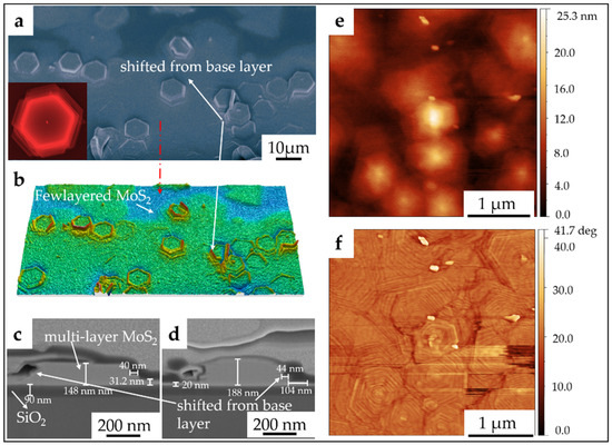
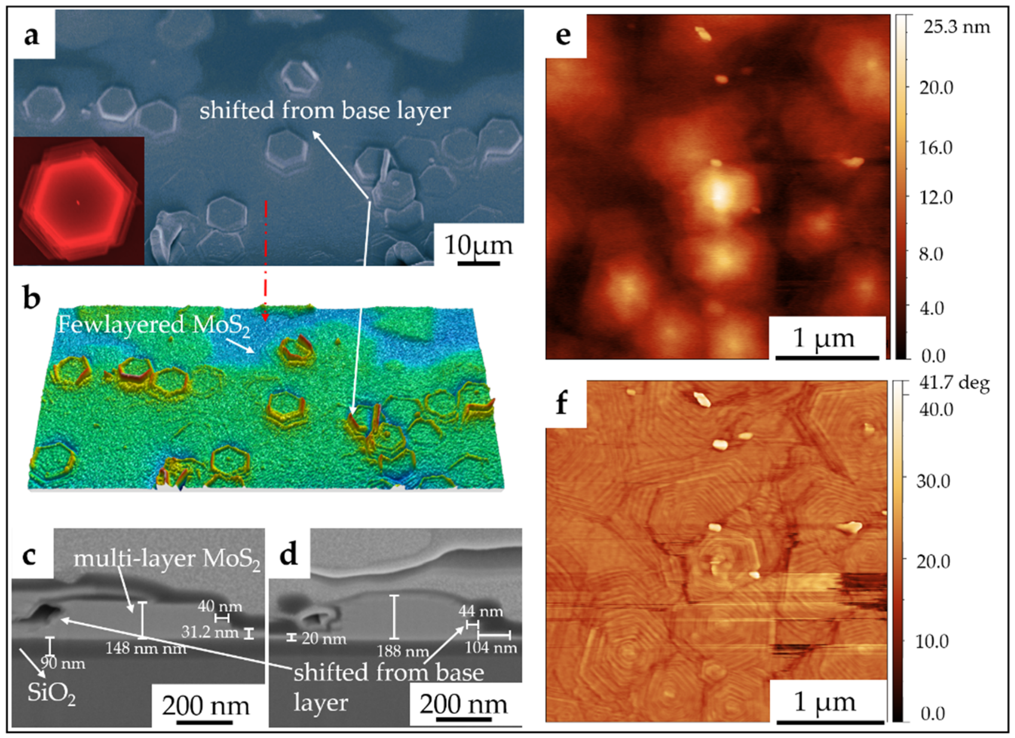
The multilayered hexagonal MoS2 structures were investigated with SEM, AFM, and FIB to elucidate their morphological characteristics. The detailed morphology of the multilayer hexagonal structures is presented in Figure 2. These structures exhibit a distinct vertical stacking configuration, where additional layers are formed on top of an underlying MoS2 base layer. In Figure 2a, a tilted SEM image provides clear visualization of this stacked architecture. The inset SEM image highlights that successive layers exhibit a shift with respect to the underlying layer while maintaining their crystallographic orientation. A three-dimensional representation of these structures is shown in Figure 2b, offering a comprehensive view of the multilayer arrangement. To gain further insight into the vertical growth mechanism, cross-sectional analysis was performed using FIB milling. Prior to sectioning, protective carbon and platinum layers were sequentially deposited using an electron beam to prevent surface damage. Subsequently, precise cross-sections were prepared using a gallium ion beam. The cross-sectional FIB images shown in Figure 2c,d reveal the internal morphology of the multilayer hexagonal MoS2 structures grown on the SiO2/Si substrate. The base layer appears as a relatively continuous film with a thickness of approximately 20–35 nm, while the subsequently stacked layers exhibit thicknesses in the range of 100–200 nm. A notable feature is the lateral displacement of the upper layers with respect to the base layer, with a sliding distance of ~40–100 nm. This lateral offset can be understood in the context of the growth mechanism discussed earlier. Under surface diffusion limited growth conditions, adatoms arriving on the surface preferentially attach on energetically favorable sites, such as step edges or existing terraces [33,34,35]. However, due to local variations in adatom flux, diffusion length, and attachment kinetics, the nucleation of upper layers does not necessarily occur exactly above the center of the underlying domain. Instead, slight asymmetries in mass transport to the edges lead to off-centered nucleation, which manifests as a lateral shift of the upper layers relative to the base layer. This behavior is further facilitated by the weak van der Waals interaction between layers, which allows lateral relaxation to minimize local strain and surface energy without disrupting the overall crystallographic orientation [19,20,33]. Furthermore, the FIB cross-sections do not show any voids or porous features between the stacked layers, indicating that the structures are densely packed. This suggests that the growth proceeds via continuous material incorporation rather than incomplete coalescence, consistent with a sufficiently high local precursor supply during vertical growth. However, in many cases, the upper layers exhibit a reduced lateral size compared to the base layer, forming progressively smaller hexagonal terraces. This morphological evolution can be attributed to a gradual decrease in effective adatom supply at higher layers due to limited vertical mass transport from the gas phase and shadowing effects, as well as Ehrlich–Schwoebel growth instabilities [23,24].
Figure 2.
Morphological details of hexagonal-shaped multilayered MoS2 structures. (a) SEM (tilted) image of the multilayered hexagonal MoS2 structures. Insets show the top view of these structures. (b) Three-dimensional overview of the formation of hexagonal MoS2 structures. (c,d) Cross-sectional FIB image of multilayered MoS2 structures and its features. (e,f) AFM topography of hexagonally stacked MoS2 structures.
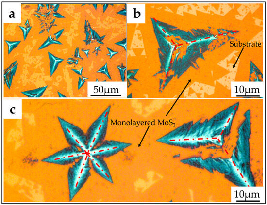
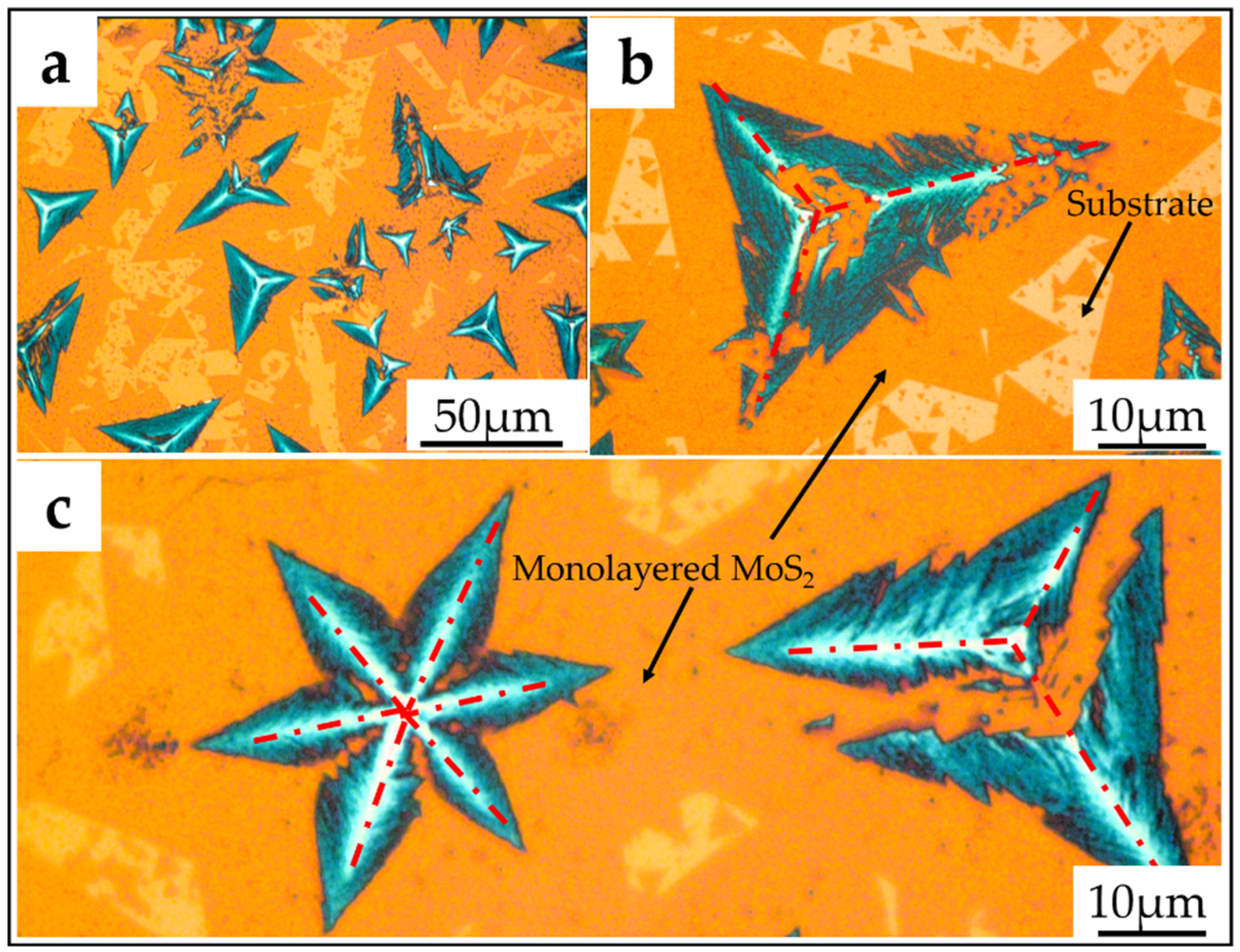
In contrast to the multilayer hexagonal structures, the dendritic-shaped MoS2 domains exhibit highly anisotropic and branched morphologies, as shown in Figure 3. These structures are predominantly observed on top of an underlying monolayer or few-layer MoS2 film, where the monolayer regions appear as darker orange contrast, while the substrate is lighter. The dendritic-like structures (highlighted in green) are observed to form on top of the underlying monolayer MoS2, indicating that the pre-existing layer acts as a preferential nucleation template. The early stage of growth is marked by a well-defined triangular nucleus (outlined by red dotted lines), which reflects the anisotropic edge energetics of MoS2 under sulfur-rich conditions. This triangular core serves as a seed, from which growth proceeds outward. As growth continues, kinetic effects dominate, promoting preferential extension along specific directions and resulting in the characteristic branched dendritic morphology [10,34]. This suggests that growth initially follows a thermodynamically favored triangular configuration, consistent with anisotropic edge stability. However, as growth proceeds, the morphology deviates from equilibrium shapes due to changes in local growth conditions causing morphological instabilities [24]. The transition from compact triangular domains to dendritic structures can be attributed to a shift from thermodynamically controlled growth to kinetically dominated growth [10,34,35]. Under relatively balanced growth conditions, domain evolution is governed by minimization of edge free energy, resulting in well-defined triangular flakes. In contrast, under sulfur-rich and high precursor flux conditions, the attachment rate of adatoms exceeds their surface diffusion capability. As a result, atoms are incorporated at the first available sites rather than redistributing along energetically favorable edges. This leads to diffusion-limited growth, where material accumulates preferentially at protrusions or tips of the structure due to diffusion instabilities [23,36]. These regions experience enhanced local flux (a classical tip-effect instability), promoting accelerated growth along specific directions and giving rise to branched, fractal-like dendritic morphologies. The observed arms extending from the triangular core therefore reflect instability-driven growth rather than equilibrium shape evolution. Furthermore, the underlying SiO2/Si substrate plays a crucial role in this process. Unlike crystalline substrates, the amorphous nature of SiO2 provides a spatially non-uniform energy landscape for adatom diffusion. This lack of directional constraint allows growth to proceed along locally favorable diffusion pathways, further enhancing branching and morphological irregularity [10,34]. Nevertheless, the dendritic morphology arises from diffusion-limited kinetic growth instabilities governed by the Mo concentration gradient under extreme sulfur excess. Oxysulfide or suboxide phases are therefore not required for dendrite formation [10,29,32].
Figure 3.
Formation of dendritic MoS2 structures. (a–c) Optical microscope image of dendritic MoS2 structures on Si/SiO2 substrate.
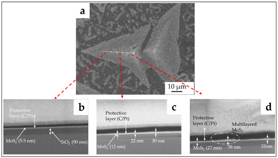
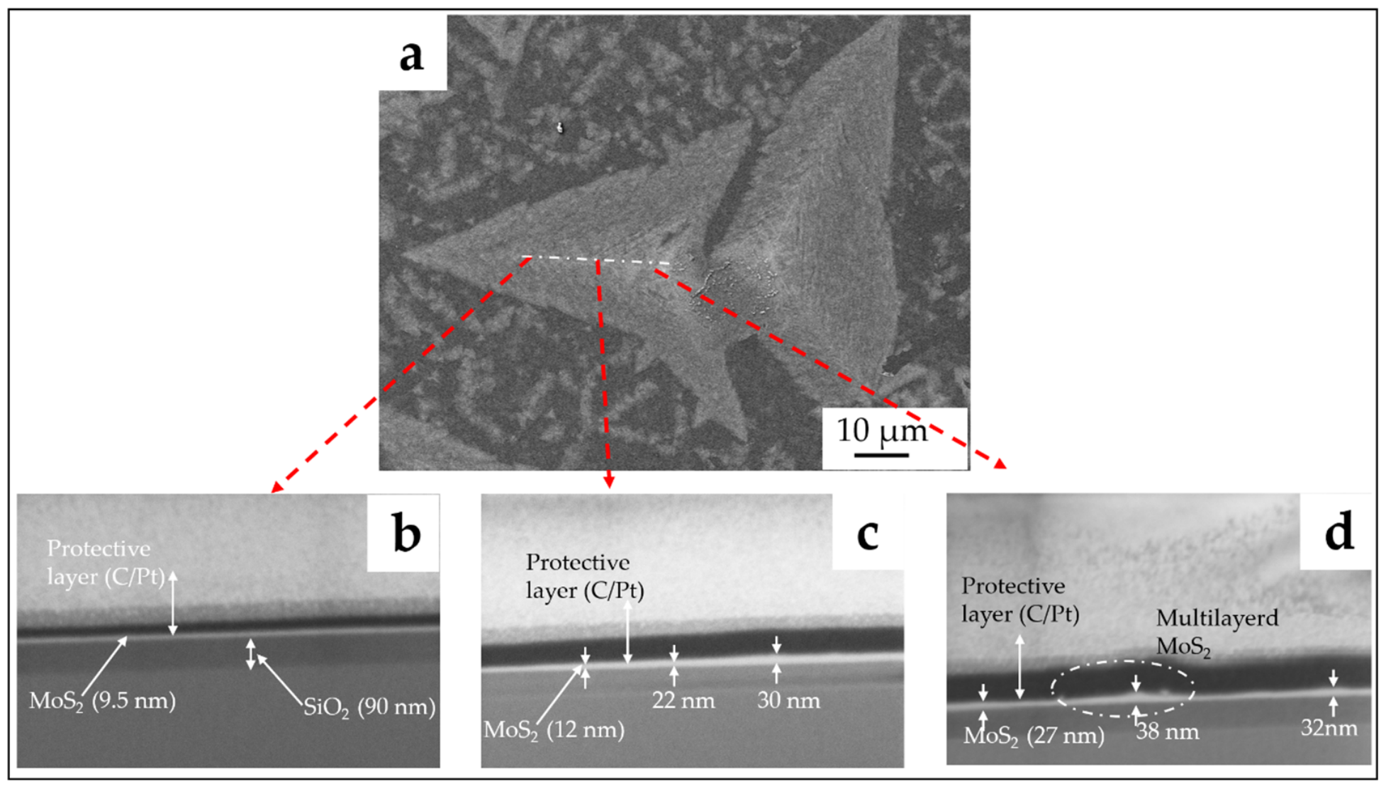
Furthermore, the internal structural continuity of the dendritic arms was investigated by performing cross-sectional FIB analysis along a dendritic structure: the arm apex, the mid-arm region, and the core/base region. Figure 4a shows the SEM image of the dendritic structure with the three FIB cut positions indicated. At all three positions (Figure 4b–d), the MoS2 film appears as a continuous, dense layer with no internal voids, gaps, or porosity, and the protective C/Pt capping layer is conformally deposited directly on top of the MoS2 surface in every cross-section, confirming the absence of subsurface discontinuities. A clear thickness gradient is observed along the arm: the apex measures approximately 9.5 nm (Figure 4b), the mid-arm region increases progressively from 12 nm to 30 nm (Figure 4c), and the core/base region reaches 27–38 nm, including a locally thicker multilayered patch (Figure 4d). This progressive thickening from tip to base is consistent with the proposed growth mechanism, in which the thinner arm tips extend rapidly via diffusion-limited, instability-driven growth, while the core and base regions accumulate additional material through continued secondary nucleation and vertical stacking over the full growth duration. For reference, optical and SEM images of the two distinct dendritic structures used for Raman/PL characterization and FIB cross-sectional analysis are provided in Figure S5, confirming that the measurements were performed on structurally distinct but nominally equivalent domains grown under identical conditions.
Figure 4.
Cross-sectional FIB and SEM analysis of a dendritic MoS2 structure. (a) SEM image of a dendritic structure with three FIB cut positions indicated by dashed red lines and arrows, corresponding to the arm apex, mid-arm region, and core/base region. (b–d) Corresponding FIB cross-sections at the apex (b), mid-arm (c), and core/base region (d), showing continuous, void-free MoS2 films with thickness increasing from 9.5 nm (b) to 12–30 nm (c) to 27–38 nm including a locally thicker multilayered patch (d). White arrows in panels (b–d) indicate the measured thickness of the MoS2 film and the protective C/Pt capping layer at each position.
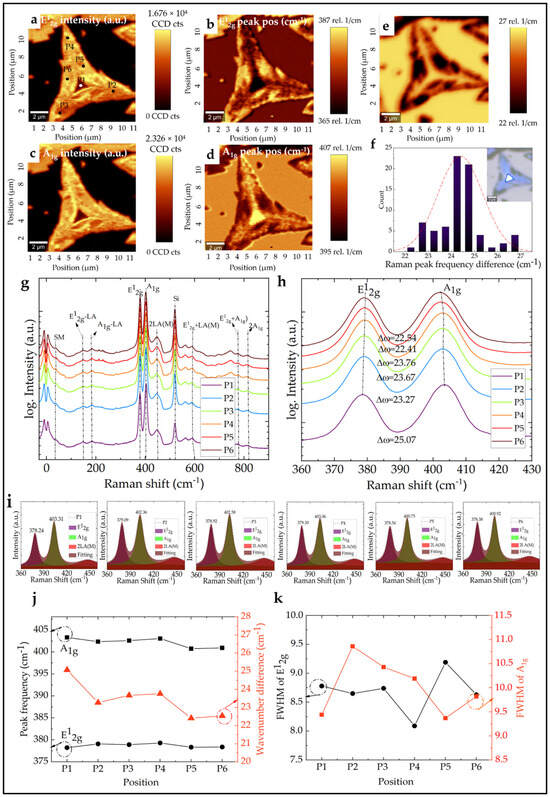
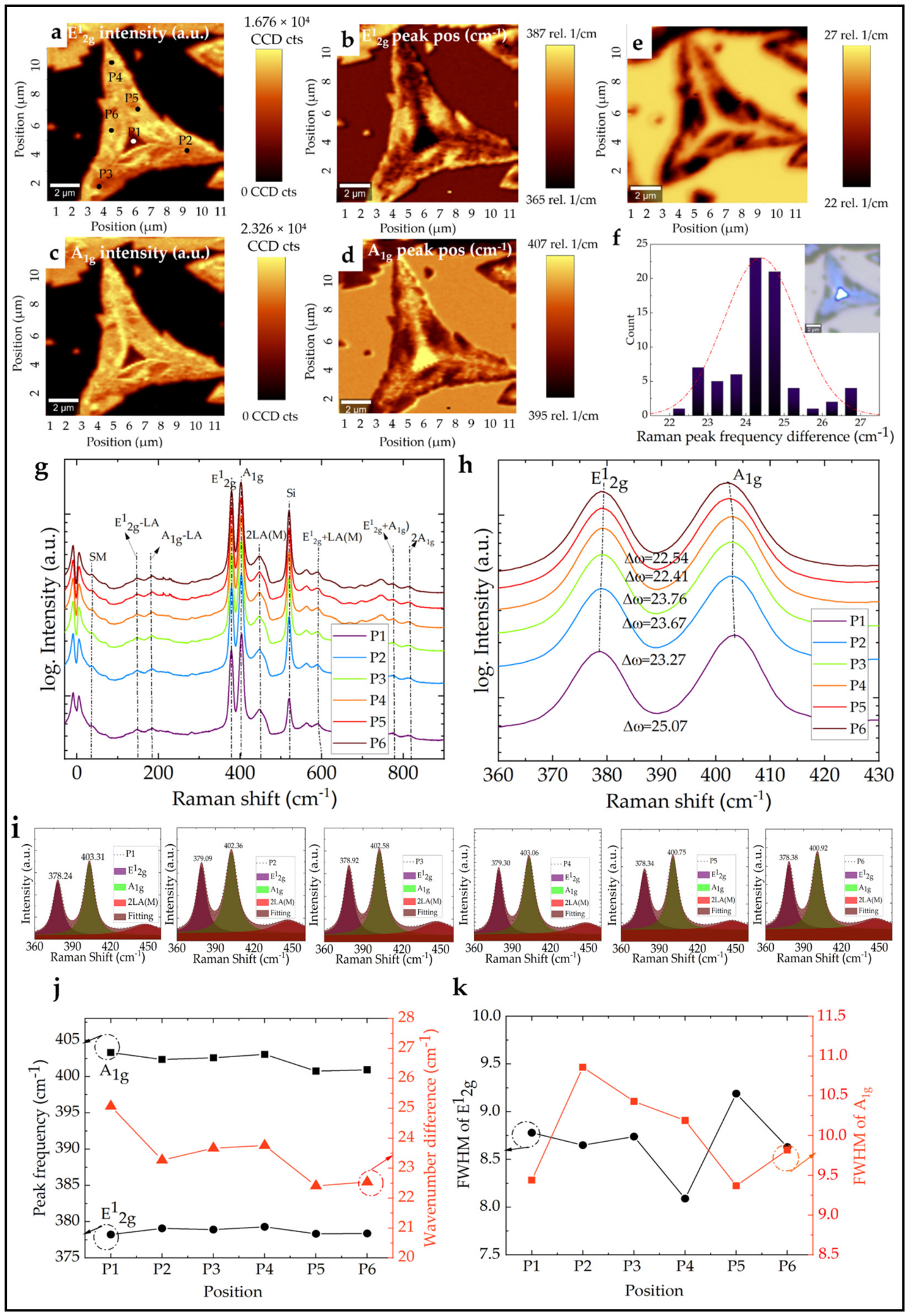
The insets in Figure 5f provide an optical image of the scanned region of the dendritic MoS2 structure. Figure 5a,c, presents Raman intensity mapping images of the E12g and A1g peaks obtained using a 488 nm laser line at room temperature. The positions where the Raman spectra were acquired are labeled P1–P6 in Figure 5a. To further elucidate the layer thickness variations, peak frequency mappings of the E12g and A1g modes were extracted from the recorded Raman mappings and shown in Figure 5b,d. In these mappings, the brightness or darkness of the colors represents the shift in the peak frequencies. In the E12g peak position Raman mapping (Figure 5b), the intensity exhibits variations corresponding to different thicknesses or layers of MoS2. The uniform color contrast in each region indicates distinct thicknesses, with brighter colors indicating thinner MoS2 layers. This observation is consistent with the understanding that as MoS2 thickness decreases, the E12g peak experiences a blue shift, which is represented by the brighter colors in the mapping. Similarly, Figure 5d shows the Raman peak frequency mapping of the A1g mode, where darker colors signify a redshift of the A1g peak. In contrast to the E12g peak mapping, the A1g peak frequency mapping shows that darker colors correspond to thinner areas, while lighter colors correspond to thicker layers of MoS2. This relationship reflects the behavior of the A1g peak, which experiences a red shift as the thickness of MoS2 increases. Additionally, Figure 5e reveals that the wavenumber difference between the characteristic peaks is increasing for the bulk layers, indicated by brighter colors, compared to the thinner layers, represented by darker shades. This trend suggests that the spectral separation between the peaks decreases as the thickness of the MoS2 layers decreases. This occurs if the measurement position is moved toward the tip of the dendritic MoS2 structure. Indeed, based on the Raman peak separation values (Δω ≈ 22.4 cm−1 at P5–P6 vs. ~25.1 cm−1 at P1), the dendritic structures exhibit a pronounced thickness gradient: the outermost base periphery at positions P5–P6 corresponds to a few-layer MoS2 region, while the central core and arm interior (P1–P4) represent a thick 3D multilayer crystal, consistent with the cross-sectional FIB-measured thicknesses of 9.5–38 nm.
Figure 5.
Raman analysis of dendritic MoS2 structures. (a,b) Raman intensity and peak frequency mappings of the E12g peak of MoS2 with the six measurement points P1–P6. (c,d) Raman intensity and peak frequency mappings of the A1g peak of MoS2. (e) Raman peak frequency difference mapping between the E12g and A1g peaks of MoS2. (f) Statistical representation of the peak frequency difference of E12g and A1g peaks of MoS2 at different measurement positions; inset shows the optical image of the scanned area. (g) Raman spectral analysis obtained from six different positions on dendritic MoS2 structures. (h) Characteristic Raman peaks of MoS2 obtained from positions P1–P6 showing the E12g and A1g modes with their respective Δω values. (i) Fitted E12g, A1g, and 2LA(M) Lorentzian peaks of MoS2 and their respective peak position values at positions P1–P6. (j) Characteristic Raman peak positions of E12g (black circles) and A1g (black squares) (left axis) and their wavenumber difference Δω (orange triangles, right axis) with respect to measurement positions P1–P6. (k) FWHM of the E12g (black circles, left axis) and A1g (orange squares, right axis) peaks of MoS2 across positions P1–P6.
Furthermore, Figure 5f presents a statistical distribution of these differences observed from various points across the sample. This distribution presents the consistency and variability of the wavenumber differences between characteristic peaks dependent on the layer thickness throughout the sample. Figure 5g shows the spectral analysis obtained from six different points on the dendritic structure. Within the spectrum, the E12g peak appears between 378 cm−1 and 380 cm−1, while the A1g peak is between 400 cm−1 and 403 cm−1, representing the fundamental vibrational modes of MoS2 [37,38]. In addition to these characteristic modes, the analysis reveals other signals associated with MoS2. Lower-frequency combination modes including E12g-LA at ~148 cm−1 and A1g-LA at ~180 cm−1 are also observed [38,39,40,41]. The double longitudinal acoustic phonon mode (2LA) is observed at ~453 cm−1. Additional higher-frequency combination modes are also present, including (E12g + LA) at ~598 cm−1, (E12g + A1g) at ~780 cm−1, and (2A1g) at ~820 cm−1 [38,39,40,41]. These shear modes (SMs) involve the in-plane motion of metal and chalcogen atoms, while the layer breathing mode (LBM) entails the out-of-plane motion of metal and chalcogen atoms. Notably, while the SMs and LBMs are absent in single layers of MoS2, they exhibit characteristic blue and red shifts, respectively, as the layer number increases [39,40,42].
Figure 5h illustrates the dependency of the deviation of characteristic peaks of MoS2 on the layer numbers. Analysis reveals that as the layer number decreases, the E12g and A1g peaks exhibit slight shifts in their frequencies: the E12g peak undergoes a blue shift, while the A1g peak experiences redshift. The fitted E12g, A1g, and 2LA(M) peaks of MoS2 and their respective peak position values respective to each position are shown in Figure 5i. In Figure 5j, the variation in these characteristic peaks across six different positions is depicted along with their wavenumber difference. Notably, from positions P1 to P4, the E12g and A1g peak positions show minimal change. However, at positions P5 and P6, the E12g peak experiences a slight stiffening (~2 cm−1, from 378.2 to 378.4 cm−1), while the A1g mode notably softens (~2.4 cm−1, from 403.3 to 400.9 cm−1). The stiffening and softening of the peaks decrease the wavenumber difference from Δω ~25.1 to ~22.4 cm−1, indicating a change in the characteristic nature of the MoS2 thickness from multilayered to few-layered formation [38,43]. The frequency variation in the E12g and A1g modes with layer thickness can be explained using the van der Waals force model [44,45,46]. With an increase in layer number, the inter-layer van der Waals force in MoS2 strengthens, suppressing atom vibrations and resulting in higher force constants [46]. Consequently, the E12g peak undergoes a redshift due to the shorter intra-layer S–Mo–S distance in thinner MoS2 layers. Furthermore, the anomalous redshift of E12g with increasing layer thickness can be attributed to structural changes or an increase in long-range Coulombic interlayer interactions, particularly involving Mo atoms, as the E12g mode involves in-plane Mo atom vibrations. In contrast, the A1g mode is less affected by these Coulomb potential screening effects, as it primarily involves out-of-plane S atom vibrations [43,46,47]. The FWHM widths of these Raman peaks, depicted in Figure 5k, further support these observations. The FWHM of the E12g peak varies between 8.1 and 9.2 cm−1 across all positions, with no clear monotonic trend, while the A1g FWHM ranges from 9.4 cm−1 at P1 to 10.9 cm−1 at P2, before decreasing to 9.4–9.8 cm−1 at P5–P6, consistent with broader linewidths in the thicker multilayer interior and narrower linewidths in the thinner base regions.
To decouple the contributions of strain, charge doping, and electron–phonon coupling to the observed anti-correlated mode shifts, the I(A1g)/I(E12g) integrated intensity ratio was extracted for all positions, P1–P6 and plotted alongside Δω in Figure S6. The ratio shows a general decreasing trend from 1.37 at P1 to 1.17 at P6, consistent with a progressive reduction in electron–phonon coupling strength toward the thinner base regions, where reduced interlayer van der Waals coupling weakens dielectric screening and lowers the local carrier density available for A1g phonon renormalization [38,43,46]. All ratio values remain above unity across all positions, which is consistent with relatively low sulfur vacancy concentrations at the probed positions—significant vacancy-induced excess electron doping would selectively suppress A1g intensity and drive the ratio below unity [38,43]. However, this indirect proxy cannot substitute for direct quantitative compositional analysis, and local non-stoichiometry—particularly at the edges and branching points of the dendritic structure where kinetically driven adatom incorporation may be less selective—cannot be excluded based on optical methods alone. The anti-correlated shifts at P4–P5, where Δω decreases from ~23.8 to ~22.4 cm−1 while I(A1g)/I(E12g) simultaneously decreases, are therefore self-consistently explained: both trends reflect the same thickness-driven reduction in interlayer coupling and carrier density at the dendritic periphery [38,43,46]. The concurrent blue shift of the E12g mode at P5–P6 relative to P1–P4 is attributed to reduced interlayer Coulomb interactions and weakened van der Waals coupling in the thinner peripheral regions. It is noted that the absolute positions of both modes are downshifted relative to pristine monolayer reference values, consistent with the presence of tensile strain or structural defects contributing to phonon softening across the entire dendritic structure [46,47,48,49].
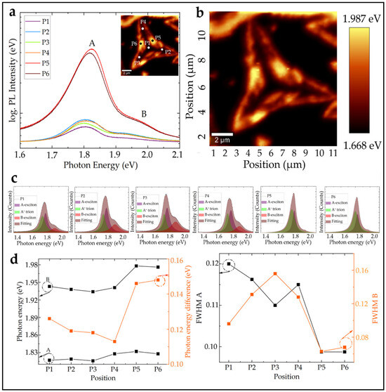
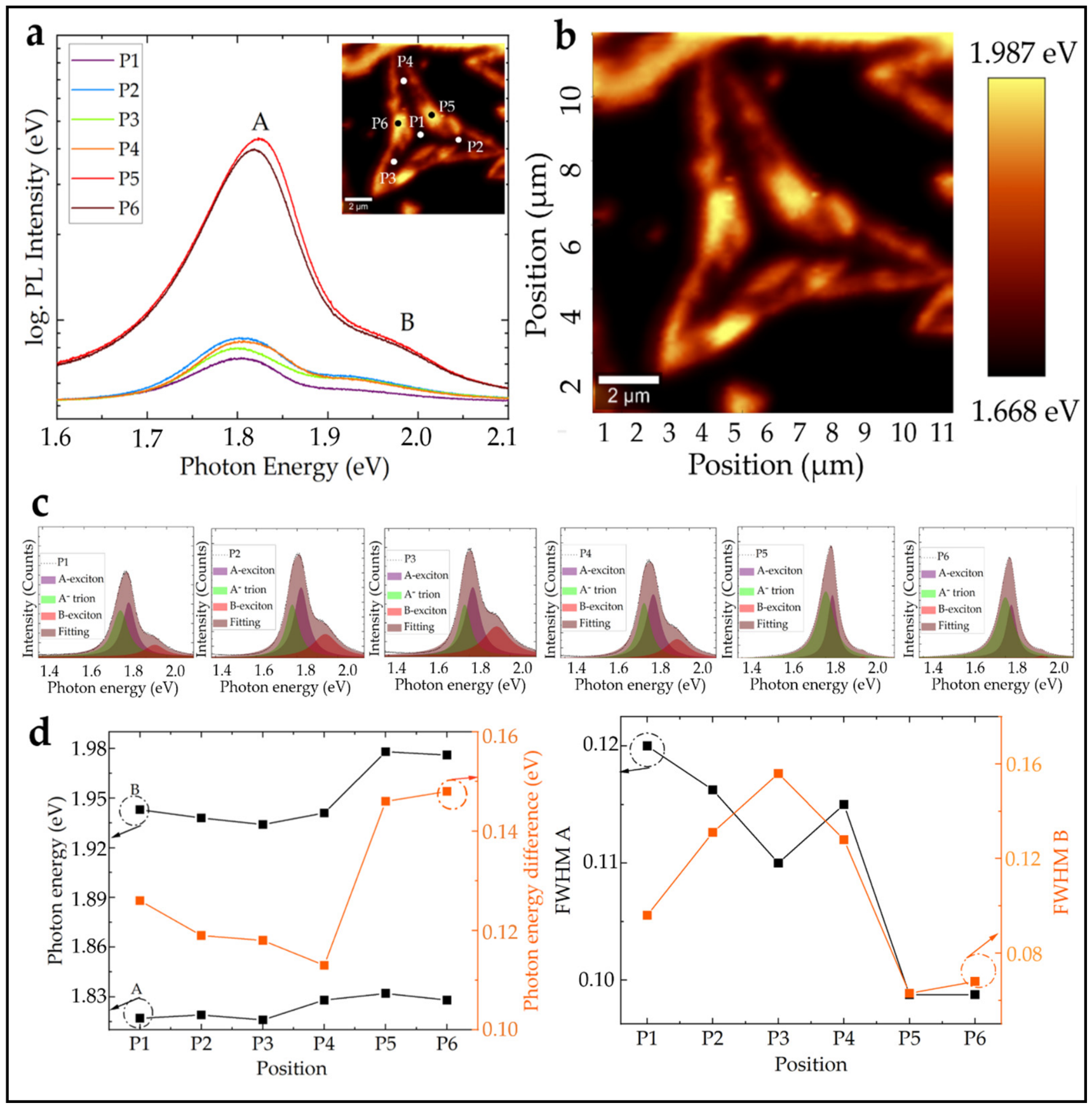
The room-temperature photoluminescence (PL) response of the dendritic MoS2 structures (Figure 6) provides further insight into their thickness-dependent optical properties and local electronic environment. As shown in Figure 6a, the PL spectra acquired from positions P1–P6 exhibit two prominent features corresponding to the A and B excitonic transitions. These peaks originate from direct bandgap transitions at the K-point, where the splitting of the valence band due to spin–orbit coupling gives rise to the A (lower energy) and B (higher energy) excitons [50,51].
Figure 6.
Photoluminescence analysis of dendritic MoS2 structure. (a) PL spectra obtained from the six points on the dendritic MoS2 structure. Insets show the PL intensity mapping of dendritic MoS2 structure. (b) PL peak intensity mapping of dendritic structure. (c) PL characterization of MoS2 structures, with dotted lines indicating data points, while solid lines are the fitting functions. (d) Dependency of PL peak positions with six different positions on dendritic MoS2 structure. Inset shows FWHM of characteristic PL peaks of MoS2.
As shown in Figure 6, a clear spatial variation in PL intensity is observed from the mapping, where thinner regions exhibit significantly higher emission intensity, consistent with a direct bandgap transition, while thicker (bulk-like) regions appear darker due to the indirect bandgap transition characteristic of multilayer MoS2. The abrupt blue shift in PL emission observed at positions P5 and P6 relative to P1–P4 directly reflects the thinner layer character of the dendritic base regions, where the direct bandgap transition dominates, as confirmed by the significantly enhanced PL intensity at these positions (Figure 6a,b). In thicker multilayer regions (P1–P4), stronger interlayer dielectric screening maintains a higher effective carrier density, shifting the spectral weight toward negatively charged trion (A−) emission, which appears ~30–40 meV below the neutral A-exciton (X0) energy and produces an apparent red shift in the observed PL peak position (Figure 6c) [52,53]. At the thinner base regions (P5–P6), reduced interlayer screening increases the exciton binding energy and lowers the local carrier density, visibly shifting the spectral weight from trion back toward neutral exciton emission and producing the observed blue shift [52,53,54]. This is further supported by the narrowing of both A and B exciton FWHM values at P5–P6 (Figure 6d), indicating relatively reduced disorder and narrower linewidths in the thinner peripheral regions compared to the thicker multilayer interior [7,10,35]. The sharp increase in B-exciton energy to ~1.987 eV at P5, combined with the A–B energy separation of ~0.13–0.158 eV, remains within the established range for MoS2 and confirms that the spectral changes arise from thickness-driven trion/exciton balance rather than structural degradation [39,52,53].
Moreover, the relatively broader FWHM linewidths in the thicker multilayer regions (P1–P4) further reflect increased disorder, lattice distortion, and enhanced exciton–phonon scattering due to higher defect density, consistent with inhomogeneous broadening in CVD-grown multilayer MoS2 [7,10,35].
4. Conclusions
In this work, the morphology of CVD-grown MoS2 microstructures was investigated as a function of nominal MoO3 and sulfur source loading under otherwise fixed APCVD conditions. Since reaction-zone partial pressures were not directly measured, the reported Mo ratios should be understood as nominal precursor loading ratios rather than absolute vapor-phase ratios. At relatively high MoO3 loading, growth was dominated by a high nucleation density, resulting in compact hexagonal and quasi-circular single- or few-layer domains. A slight reduction in Mo precursor concentration promoted diffusion-assisted growth and secondary nucleation on pre-existing domains, leading to multilayer hexagonal structures with aligned or slightly rotated stacked layers. Cross-sectional FIB analysis revealed dense vertical stacking without void formation, while lateral offsets between successive layers indicated off-centered nucleation and interlayer relaxation during growth. Further reduction in MoO3 concentration combined with increased sulfur supply shifted the system toward sulfur-rich conditions, producing large triangular domains through anisotropic edge stabilization. At the highest nominal sulfur loading, morphology transitioned into branched dendritic structures. This trend is consistent with a shift from compact edge-stabilized growth toward kinetically limited, diffusion-influenced aggregation, although quantitative extraction of supersaturation, precursor flux, or edge kinetic parameters were not performed in this study. Raman and photoluminescence analyses confirmed a strong correlation between morphology, thickness, and optical properties. The layer-dependent variation in the E12g and A1g Raman modes, together with the evolution of their peak separation, revealed the coexistence of multilayer and few-layer regions within the dendritic structures. Raman and photoluminescence analyses confirmed a strong correlation between morphology, layer thickness, and optical properties. The dendritic structures are 3D multilayer crystals exhibiting a pronounced thickness gradient from the thick multilayer core and arm interior—consistent with the FIB-measured cross-sectional thicknesses of 9.5–38 nm—to thinner few-layer regions exclusively at the outermost base periphery. The layer-dependent variation in the E12g and A1g Raman modes and the evolution of their peak separation (Δω decreasing from ~25 cm−1 at the multilayer interior to ~22 cm−1 at the peripheral positions P5–P6) confirm this thickness gradient quantitatively. Photoluminescence measurements further showed enhanced emission intensity and blue-shifted excitonic transitions at the thin peripheral positions P5–P6, consistent with reduced interlayer coupling and a thickness-driven shift in trion/exciton spectral balance toward neutral exciton emission, while the thicker interior regions exhibit reduced PL intensity and red-shifted excitonic transitions consistent with stronger interlayer dielectric screening and increased non-radiative recombination.
Supplementary Materials
The following supporting information can be downloaded at https://www.mdpi.com/article/10.3390/cryst16080480/s1, Figure S1: Time-varied SEM images of CVD-grown MoS2 at fixed precursor conditions (MoO3 = 10 mg, S = 300 mg) for growth durations of (a) 5 min, (b) 10 min, (c) 15 min, (d) 20 min, (e) 25 min, and (f) 30 min. Figure S2: (a) Schematic illustration of the CVD reactor, depicting the position of precursors, growth substrate and lamb heating. (b) The temperature-time profile of the CVD process for the growth of MoS2 structures. Table S1: Precursor ratio utilized, and the respective morphology obtained. Figure S3: Raman spectra of monolayer MoS2 triangular domains (MoO3 = 10 mg, S = 300 mg). The E12g–A1g peak separations of Δω = 19.02 cm−1 and Δω = 19.01 cm−1 at two spatial positions (optical image inset) confirm monolayer character. Table S2: Estimated equilibrium vapor-pressure ceilings and lower-bound precursor source-depletion times under the APCVD conditions used in this work. Figure S4: X-ray diffraction patterns of CVD-grown MoS2 structures representing the hexagonal (MoO3 = 100 mg, S = 200 mg), triangular (MoO3 = 10 mg, S = 300 mg), and dendritic (MoO3 = 10 mg, S = 400 mg) morphological regimes, indexed to the 2H-MoS2 phase (PDF 37-1492). Figure S5: Optical image of the dendritic MoS2 structure used for Raman and PL measurements (left), showing a star-shaped morphology with thin luminescent base periphery and thicker central ridge. SEM image of the separate structure used for FIB cross-sectional analysis (right), showing a compact bulk-like morphology from which the 9.5–38 nm cross-sectional thicknesses were obtained. Both structures grown under identical conditions (MoO3 = 10 mg, S = 400 mg) from independently prepared samples. Figure S6: I(A1g)/I(E12g) Raman intensity ratio (left axis, teal bars) and peak separation Δω (right axis, orange line) across positions P1–P6 of the dendritic MoS2 structure. References [55,56,57,58,59,60,61] are cited in the Supplementary Materials.
Author Contributions
Conceptualization, S.M. and J.P.; methodology, S.M.; software, S.M.; validation, S.M., J.P., B.H., and V.K.; formal analysis, S.M., J.P., and V.K.; investigation, S.M., J.P., B.H., D.F., and V.K.; resources, J.P.; data curation, S.M., D.F., B.H., and V.K.; writing—original draft preparation, S.M. and J.P.; writing—review and editing, S.M., J.P., B.H., and V.K.; visualization, S.M. and J.P.; supervision, J.P. and H.O.J.; project administration, J.P.; funding acquisition, J.P. All authors have read and agreed to the published version of the manuscript.
Funding
The financial support of this research by the Carl Zeiss Foundation (Carl-Zeiss-Stiftung) under Contract P2018-01-002. We also acknowledge for the support of publication costs by the Open Access Publication Fund of the Technische Universität Ilmenau.
Data Availability Statement
The data that support the findings of this study are available from the corresponding authors, S.M. and J.P., upon reasonable request.
Acknowledgments
The authors acknowledge the financial support of this research by the Carl Zeiss Foundation under Contract P2018-01-002. The authors would like to express special gratitude for all the support provided by the Center of Micro and Nanotechnologies (ZMN), TU Ilmenau. The authors are grateful to Henry Romanus for his timely support and valuable contributions during the revision and preparation of the manuscript.
Conflicts of Interest
The authors declare no conflicts of interest.
References
- Radisavljevic, B.; Radenovic, A.; Brivio, J.; Giacometti, V.; Kis, A. Single-layer MoS2 transistors. Nat. Nanotechnol. 2011, 6, 147. [Google Scholar] [CrossRef] [Scilit] [PubMed]
- Wang, Q.H.; Kalantar-Zadeh, K.; Kis, A.; Coleman, J.N.; Strano, M.S. Electronics and optoelectronics of two-dimensional transition metal dichalcogenides. Nat. Nanotechnol. 2012, 7, 699. [Google Scholar] [CrossRef] [Scilit] [PubMed]
- Kang, K.; Xie, S.; Huang, L.; Han, Y.; Huang, P.Y.; Mak, K.F.; Kim, C.-J.; Muller, D.; Park, J. High-mobility three-atom-thick semiconducting films with wafer-scale homogeneity. Nature 2015, 520, 656. [Google Scholar] [CrossRef] [Scilit] [PubMed]
- Van Der Zande, A.M.; Huang, P.Y.; Chenet, D.A.; Berkelbach, T.C.; You, Y.; Lee, G.-H.; Heinz, T.F.; Reichman, D.R.; Muller, D.A.; Hone, J.C. Grains and grain boundaries in highly crystalline monolayer molybdenum disulphide. Nat. Mater. 2013, 12, 554. [Google Scholar] [CrossRef] [Scilit] [PubMed]
- Singh, A.; Sharma, M.; Singh, R. NaCl-assisted CVD growth of large-area high-quality trilayer MoS2 and the role of the concentration boundary layer. Cryst. Growth Des. 2021, 21, 4940. [Google Scholar] [CrossRef] [Scilit]
- Wang, S.; Rong, Y.; Fan, Y.; Pacios, M.; Bhaskaran, H.; He, K.; Warner, J.H. Shape evolution of monolayer MoS2 crystals grown by chemical vapor deposition. Chem. Mater. 2014, 26, 6371. [Google Scholar] [CrossRef] [Scilit]
- Zhu, Z.; You, J.; Zhu, D.; Jiang, G.; Zhan, S.; Wen, J.; Xia, Q. Effect of precursor ratio on the morphological and optical properties of CVD-grown monolayer MoS2 nanosheets. Mater. Res. Express 2021, 8, 045008. [Google Scholar] [CrossRef] [Scilit]
- Xu, H.-J.; Mi, J.-S.; Li, Y.; Zhang, B.; Cong, R.-D.; Fu, G.-S.; Yu, W. Nucleation mechanism and morphology evolution of MoS2 flakes grown by chemical vapor deposition. Chin. Phys. B 2017, 26, 128102. [Google Scholar] [CrossRef] [Scilit]
- Özden, A.; Ay, F.; Sevik, C.; Perkgöz, N.K. CVD growth of monolayer MoS2: Role of growth zone configuration and precursors ratio. Jpn. J. Appl. Phys. 2017, 56, 06GG05. [Google Scholar] [CrossRef] [Scilit]
- Xu, W.; Li, S.; Zhou, S.; Lee, J.K.; Wang, S.; Sarwat, S.G.; Wang, X.; Bhaskaran, H.; Pasta, M.; Warner, J.H. Large dendritic monolayer MoS2 grown by atmospheric pressure chemical vapor deposition for electrocatalysis. ACS Appl. Mater. Interfaces 2018, 10, 4630. [Google Scholar] [CrossRef] [Scilit] [PubMed]
- Cao, D.; Shen, T.; Liang, P.; Chen, X.; Shu, H. Role of chemical potential in flake shape and edge properties of monolayer MoS2. J. Phys. Chem. C 2015, 119, 4294. [Google Scholar] [CrossRef] [Scilit]
- Govind Rajan, A.; Warner, J.H.; Blankschtein, D.; Strano, M.S. Generalized mechanistic model for the chemical vapor deposition of 2D transition metal dichalcogenide monolayers. ACS Nano 2016, 10, 4330. [Google Scholar] [CrossRef] [Scilit] [PubMed]
- Mouloua, D.; Rajput, N.; Blach, J.-F.; Lejeune, M.; El Marssi, M.; El Khakani, M.; Jouiad, M. Fabrication control of MoS2/MoO2 nanocomposite via chemical vapor deposition for optoelectronic applications. Mater. Sci. Eng. B 2022, 286, 116035. [Google Scholar] [CrossRef] [Scilit]
- Sin, C.-K.; Zhu, J. Determining Equilibrium Shapes of MoS2: Modified Algorithm, Edge Reconstructions with S and O, and Temperature Effects. J. Phys. Chem. C 2021, 125, 4828. [Google Scholar] [CrossRef] [Scilit]
- Ahn, G.H.; Amani, M.; Rasool, H.; Lien, D.-H.; Mastandrea, J.P.; Ager, J.W., III; Dubey, M.; Chrzan, D.C.; Minor, A.M.; Javey, A. Strain-engineered growth of two-dimensional materials. Nat. Commun. 2017, 8, 608. [Google Scholar] [CrossRef] [Scilit] [PubMed]
- Liu, Y.; Ghosh, R.; Wu, D.; Ismach, A.; Ruoff, R.; Lai, K. Mesoscale imperfections in MoS2 atomic layers grown by a vapor transport technique. Nano Lett. 2014, 14, 4682. [Google Scholar] [CrossRef] [Scilit] [PubMed]
- Kalikmanov, V.I. Nucleation Theory; Springer: Berlin/Heidelberg, Germany, 2012. [Google Scholar]
- Najmaei, S.; Liu, Z.; Zhou, W.; Zou, X.; Shi, G.; Lei, S.; Yakobson, B.I.; Idrobo, J.-C.; Ajayan, P.M.; Lou, J. Vapour phase growth and grain boundary structure of molybdenum disulphide atomic layers. Nat. Mater. 2013, 12, 754. [Google Scholar] [CrossRef] [Scilit] [PubMed]
- Ly, T.H.; Zhao, J.; Kim, H.; Han, G.H.; Nam, H.; Lee, Y.H. Vertically conductive MoS2 spiral pyramid. Adv. Mater. 2016, 28, 7723. [Google Scholar] [CrossRef] [Scilit] [PubMed]
- Samaniego-Benitez, J.E.; Mendoza-Cruz, R.; Bazán-Díaz, L.; Garcia-Garcia, A.; Arellano-Jimenez, M.J.; Perez-Robles, J.F.; Plascencia-Villa, G.; Velázquez-Salazar, J.J.; Ortega, E.; Favela-Camacho, S.E. Synthesis and structural characterization of MoS2 micropyramids. J. Mater. Sci. 2020, 55, 12203. [Google Scholar] [CrossRef] [Scilit]
- Wulff, G. Xxv. zur frage der geschwindigkeit des wachsthums und der auflösung der krystallflächen. Z. Für Krist.-Cryst. Mater. 1901, 34, 449. [Google Scholar] [CrossRef] [Scilit]
- Markov, I.V. Crystal Growth for Beginners: Fundamentals of Nucleation, Crystal Growth, and Epitaxy; World Scientific: Singapore, 2003. [Google Scholar]
- Politi, P.; Grenet, G.; Marty, A.; Ponchet, A.; Villain, J. Instabilities in crystal growth by atomic or molecular beams. Phys. Rep. 2000, 324, 271. [Google Scholar] [CrossRef] [Scilit]
- Krug, J. Four lectures on the physics of crystal growth. Phys. A Stat. Mech. Appl. 2002, 313, 47. [Google Scholar] [CrossRef] [Scilit]
- Jäger-Waldau, A.; Lux-Steiner, M.C.; Bucher, E.; Scandella, L.; Schumacher, A.; Prins, R. MoS2 thin films prepared by sulphurization. Appl. Surf. Sci. 1993, 65, 465. [Google Scholar] [CrossRef] [Scilit]
- Hadouda, H.; Pouzet, J.; Bernede, J.; Barreau, A. MoS2 thin film synthesis by soft sulfurization of a molybdenum layer. Mater. Chem. Phys. 1995, 42, 291. [Google Scholar] [CrossRef] [Scilit]
- Py, M.; Haering, R. Structural destabilization induced by lithium intercalation in MoS2 and related compounds. Can. J. Phys. 1983, 61, 76. [Google Scholar] [CrossRef] [Scilit]
- Chhowalla, M.; Shin, H.S.; Eda, G.; Li, L.-J.; Loh, K.P.; Zhang, H. The chemistry of two-dimensional layered transition metal dichalcogenide nanosheets. Nat. Chem. 2013, 5, 263. [Google Scholar] [CrossRef] [Scilit] [PubMed]
- Li, X.; Zhang, S.; Chen, S.; Zhang, X.; Gao, J.; Zhang, Y.-W.; Zhao, J.; Shen, X.; Yu, R.; Yang, Y. Mo concentration controls the morphological transitions from dendritic to semicompact, and to compact growth of monolayer crystalline MoS2 on various substrates. ACS Appl. Mater. Interfaces 2019, 11, 42751. [Google Scholar] [CrossRef] [Scilit] [PubMed]
- Ma, J.; Li, X.; Gan, L.; Zhang, S.; Cao, Y.; Nie, Z.; Wang, X.; Ma, D.; He, L.; Nie, J. Controlling the dendritic structure and the photo-electrocatalytic properties of highly crystalline MoS2 on sapphire substrate. 2D Mater. 2018, 5, 031015. [Google Scholar] [CrossRef] [Scilit]
- Wu, D.; Min, T.; Zhou, J.; Li, C.; Ma, G.; Lu, G.; Xia, M.; Gu, Z. Effect of Substrate symmetry on the dendrite morphology of MoS2 Film synthesized by CVD. Sci. Rep. 2017, 7, 15166. [Google Scholar] [CrossRef] [Scilit] [PubMed]
- Chowdhury, S.; Roy, A.; Alam, M.H.; Pramanik, T.; Depoy, J.; Chrostowski, R.; Mangolini, F.; Akinwande, D.; Banerjee, S.K. Role of hydrogen in suppressing secondary nucleation in chemical vapor-deposited MoS2. ACS Appl. Electron. Mater. 2022, 4, 6133. [Google Scholar] [CrossRef] [Scilit]
- Sarma, P.V.; Patil, P.D.; Barman, P.K.; Kini, R.N.; Shaijumon, M.M. Controllable growth of few-layer spiral WS2. RSC Adv. 2016, 6, 376. [Google Scholar] [CrossRef] [Scilit]
- Zhang, Z.; Lagally, M.G. Atomistic processes in the early stages of thin-film growth. Science 1997, 276, 377. [Google Scholar] [CrossRef] [Scilit] [PubMed]
- Rotunno, E.; Bosi, M.; Seravalli, L.; Salviati, G.; Fabbri, F. Influence of organic promoter gradient on the MoS2 growth dynamics. Nanoscale Adv. 2020, 2, 2352. [Google Scholar] [CrossRef] [Scilit] [PubMed]
- Barabási, A.-L.; Stanley, H.E. Fractal Concepts in Surface Growth; Cambridge University Press: Cambridge, UK, 1995. [Google Scholar]
- Windom, B.C.; Sawyer, W.; Hahn, D.W. A Raman spectroscopic study of MoS2 and MoO3: Applications to tribological systems. Tribol. Lett. 2011, 42, 301. [Google Scholar] [CrossRef] [Scilit]
- Li, H.; Zhang, Q.; Yap, C.C.R.; Tay, B.K.; Edwin, T.H.T.; Olivier, A.; Baillargeat, D. From bulk to monolayer MoS2: Evolution of Raman scattering. Adv. Funct. Mater. 2012, 22, 1385. [Google Scholar] [CrossRef] [Scilit]
- O’Brien, M.; Scheuschner, N.; Maultzsch, J.; Duesberg, G.S.; McEvoy, N. Raman spectroscopy of suspended MoS2. Phys. Status Solidi (B) 2017, 254, 1700218. [Google Scholar] [CrossRef] [Scilit]
- O’Brien, M.; McEvoy, N.; Hanlon, D.; Hallam, T.; Coleman, J.N.; Duesberg, G.S. Mapping of low-frequency Raman modes in CVD-grown transition metal dichalcogenides: Layer number, stacking orientation and resonant effects. Sci. Rep. 2016, 6, 19476. [Google Scholar] [CrossRef] [Scilit] [PubMed]
- Placidi, M.; Dimitrievska, M.; Izquierdo-Roca, V.; Fontané, X.; Castellanos-Gomez, A.; Pérez-Tomás, A.; Mestres, N.; Espindola-Rodriguez, M.; López-Marino, S.; Neuschitzer, M. Multiwavelength excitation Raman scattering analysis of bulk and two-dimensional MoS2: Vibrational properties of atomically thin MoS2 layers. 2D Mater. 2015, 2, 035006. [Google Scholar] [CrossRef] [Scilit]
- Zhang, X.; Han, W.; Wu, J.; Milana, S.; Lu, Y.; Li, Q.; Ferrari, A.; Tan, P. Raman spectroscopy of shear and layer breathing modes in multilayer MoS2. Phys. Rev. B 2013, 87, 115413. [Google Scholar] [CrossRef] [Scilit]
- Chakraborty, B.; Matte, H.R.; Sood, A.; Rao, C. Layer-dependent resonant Raman scattering of a few layer MoS2. J. Raman Spectrosc. 2013, 44, 92. [Google Scholar]
- Ye, M.; Winslow, D.; Zhang, D.; Pandey, R.; Yap, Y.K. Recent Advancement on the Optical Properties of Two-Dimensional Molybdenum Disulfide (MoS2) Thin Films. Photonics 2015, 2, 288–307. [Google Scholar] [CrossRef] [Scilit]
- Bromley, R. The lattice vibrations of the MoS2 structure. Philos. Mag. A J. Theor. Exp. Appl. Phys. 1971, 23, 1417. [Google Scholar] [CrossRef] [Scilit]
- Lee, C.; Yan, H.; Brus, L.E.; Heinz, T.F.; Hone, J.; Ryu, S. Anomalous lattice vibrations of single-and few-layer MoS2. ACS Nano 2010, 4, 2695. [Google Scholar] [CrossRef] [Scilit] [PubMed]
- Gonze, X.; Lee, C. Dynamical matrices, Born effective charges, dielectric permittivity tensors, and interatomic force constants from density-functional perturbation theory. Phys. Rev. B 1997, 55, 10355. [Google Scholar] [CrossRef] [Scilit]
- Tan, C.; Wong, W.; Ng, S.; Wong, H.; Leung, C.; Mak, C. Raman studies of MoS2 under strain at different uniaxial directions. Vacuum 2018, 153, 274. [Google Scholar] [CrossRef] [Scilit]
- Rice, C.; Young, R.; Zan, R.; Bangert, U.; Wolverson, D.; Georgiou, T.; Jalil, R.; Novoselov, K. Raman-scattering measurements and first-principles calculations of strain-induced phonon shifts in monolayer MoS2. Phys. Rev. B—Condens. Matter Mater. Phys. 2013, 87, 081307. [Google Scholar] [CrossRef] [Scilit]
- Splendiani, A.; Sun, L.; Zhang, Y.; Li, T.; Kim, J.; Chim, C.-Y.; Galli, G.; Wang, F. Emerging photoluminescence in monolayer MoS2. Nano Lett. 2010, 10, 1271. [Google Scholar] [CrossRef] [Scilit] [PubMed]
- Kumar, N.; Tomar, R.; Wadehra, N.; Devi, M.M.; Prakash, B.; Chakraverty, S. Growth of highly crystalline and large scale monolayer MoS2 by CVD: The role of substrate position. Cryst. Res. Technol. 2018, 53, 1800002. [Google Scholar] [CrossRef] [Scilit]
- Ross, J.S.; Wu, S.; Yu, H.; Ghimire, N.J.; Jones, A.M.; Aivazian, G.; Yan, J.; Mandrus, D.G.; Xiao, D.; Yao, W. Electrical control of neutral and charged excitons in a monolayer semiconductor. Nat. Commun. 2013, 4, 1474. [Google Scholar] [CrossRef] [Scilit] [PubMed]
- Mak, K.F.; He, K.; Lee, C.; Lee, G.H.; Hone, J.; Heinz, T.F.; Shan, J. Tightly bound trions in monolayer MoS2. Nat. Mater. 2013, 12, 207. [Google Scholar] [PubMed]
- Cheiwchanchamnangij, T.; Lambrecht, W.R. Quasiparticle band structure calculation of monolayer, bilayer, and bulk MoS2. Phys. Rev. B—Condens. Matter Mater. Phys. 2012, 85, 205302. [Google Scholar] [CrossRef] [Scilit]
- Lee, Y.-H.; Yu, L.; Wang, H.; Fang, W.; Ling, X.; Shi, Y.; Lin, C.-T.; Huang, J.-K.; Chang, M.-T.; Chang, C.-S. Synthesis and transfer of single-layer transition metal disulfides on diverse surfaces. Nano Lett. 2013, 13, 1852. [Google Scholar] [CrossRef] [Scilit] [PubMed]
- Chen, F.; Su, W. The effect of the experimental parameters on the growth of MoS2 flakes. CrystEngComm 2018, 20, 4823. [Google Scholar] [CrossRef] [Scilit]
- Dean, J.A. Lange’s Handbook of Chemistry, 14th ed.; McGraw-Hill: New York, NY, USA, 1992; p. 5.37. [Google Scholar]
- Baker, E.H. Vapour Pressure–Temperature Relation for Sulphur up to the Critical Point; The Institute of Materials, Minerals and Mining: London, UK, 1971. [Google Scholar]
- NIST Chemistry WebBook, NIST Standard Reference Database Number 69, Molybdenum Trioxide, CAS 1313-27-5, Antoine Equation Parameters. Available online: https://webbook.nist.gov/chemistry/ (accessed on 15 July 2026).
- Lyons, J.R. An Estimate of the Equilibrium Speciation of Sulfur Vapor over Solid Sulfur and Implications for Planetary At-mospheres. J. Sulfur Chem. 2008, 29, 269–279. [Google Scholar] [CrossRef] [Scilit]
- Stull, D.R. Vapor Pressure of Pure Substances. Organic and Inorganic Compounds. Ind. Eng. Chem. 1947, 39, 517–540. [Google Scholar] [CrossRef] [Scilit]
Disclaimer/Publisher’s Note: The statements, opinions and data contained in all publications are solely those of the individual author(s) and contributor(s) and not of MDPI and/or the editor(s). MDPI and/or the editor(s) disclaim responsibility for any injury to people or property resulting from any ideas, methods, instructions or products referred to in the content. |
© 2026 by the authors. Licensee MDPI, Basel, Switzerland. This article is an open access article distributed under the terms and conditions of the Creative Commons Attribution (CC BY) license.