


Abstract
In the current work, the microstructural evolution and CO2 sensing performance of tungsten trioxide (WO3) thin films synthesized by reactive DC magnetron sputtering are investigated. Three specific thicknesses of 42, 66, and 131 nm were obtained and annealed at 500 °C, resulting in a stable monoclinic P21/n phase with a strong (200) preferred orientation. Gas sensing tests toward 10,000 ppm of CO2 revealed that the 42 nm film achieves the highest sensitivity (92%) at an optimal operating temperature of 300 °C. Rietveld refinement and texture analysis (texture index, J) demonstrate that the superior performance of the thinnest film is driven by a synergy between its high surface porosity, a grain size comparable to the Debye length, and a high density of active sites on the (200) plane. While all films exhibit n-type semiconductor behavior, increasing thickness leads to microstructural densification and reduced texture, which hinders gas diffusion and operational stability. These findings establish thickness control as a critical parameter for engineering high-performance WO3-based CO2 sensors.
1. Introduction
Carbon dioxide (CO2) is one of the primary gases contributing to the greenhouse effect and is among the most concerning due to its long atmospheric lifetime. Rising global temperatures lead to increased atmospheric CO2 concentrations, creating a self-reinforcing cycle [1]. In addition, CO2 has a wide range of applications in the food, energy, and electronics industries, among others. However, whether during its production or utilization, it is essential to continuously monitor its concentration to ensure that permissible exposure limits are not exceeded, thereby preventing adverse effects on human health and the environment. Currently, CO2 sensors are relatively expensive to manufacture and maintain.
Therefore, semiconductor metal oxides—materials extensively studied for the detection of various gases—are expected to effectively address the challenges associated with CO2 sensing [2,3,4]. The sensing behavior of semiconductor metal oxides is typically interpreted through changes in electrical resistance resulting from variations in the surrounding atmosphere. This response depends on several intrinsic material factors, including surface roughness, microstructure, crystalline structure, type and concentration of defects, and the presence of dopants [5]. The scientific literature highlights that the performance of these devices is closely linked to the microstructural and morphological characteristics of the films [6,7,8,9].
Factors such as crystalline structure—which may evolve from amorphous to monoclinic, tetragonal, or orthorhombic phases under different thermal treatments—strongly influence electrical conductivity and response time [10]. Likewise, precise control over the thickness and porosity of nanostructured films is essential to maximize the surface-to-volume ratio and facilitate gas diffusion, thereby optimizing material sensitivity [11,12]. In this work, it is demonstrated that these material-related factors play a decisive role in evaluating sensitivity toward a target gas, specifically in the detection of CO2.
2. Materials and Methods
2.1. Synthesis
WO3 thin films were deposited on glass substrates by reactive sputtering using an ATC ORION 3 system (AJA International, Hingham, MA, USA). Corning 7059 glass substrates (Corning, NY, USA) were cut into small pieces to obtain individual samples for each film. After substrate preparation, tungsten trioxide thin films were deposited at room temperature by reactive DC magnetron sputtering using a high-purity tungsten target (99.99%, 2-inch diameter) applying 60 W of power. The reactive sputtering process was carried out in an Ar/O2 gas mixture with a ratio of 3:1, at a total working pressure of 0.66 Pa. The substrates were positioned at a distance of 28 cm from the magnetron source and rotated at 40 rpm to ensure uniform film deposition. Subsequently, all thin films were annealed simultaneously in a Barnstead Thermolyne Type 47,900 furnace (Thermo Fisher Scientific, Waltham, MA, USA), under ambient atmosphere. The temperature was increased at a controlled heating rate of 2 °C min−1 until reaching 500 °C, where the samples were held for 1 min. After the dwell time, the films were cooled down to room temperature using the same rate (2 °C min−1) applied during the heating stage. This thermal treatment promoted crystallization of the WO3 films and the stabilization of the monoclinic phase.
2.2. Microstructural Characterization
The crystalline phases of the tungsten trioxide thin films were identified by X-ray diffraction (XRD) using a X’pert Pro diffractometer (PANalytical, Almelo, The Netherlands) with CuKα radiation (λ = 1.5418 Å) operated in grazing incidence mode (GIXRD). Diffractograms were collected in the 2θ range from 20° to 60° with an angular step of 0.02°. Structural parameters were refined by the Rietveld method using the GSAS-II software (Lemont, IL, USA) package, 5.6.2 version [13]. The volume-average apparent crystallite size and microstrain were obtained using the same peak profile function implemented in the FullProf Suite software, 5.20 version (Grenoble, Francia) [14] through the GFourier graphical interface, version 04.06 [15].
The surface morphology of the films was examined by field emission scanning electron microscopy (FE-SEM) using a JEOL JSM-7401F (Japan Electron Optics Laboratory Co., Ltd., Tokio, Japan) microscope operated at 2 kV. Elemental composition was analyzed by energy dispersive X-ray spectroscopy (EDS) in a TEAM™ EDS Analysis System (EDAX) (AMETEK, Inc., Edison, NJ, USA) attached to the SEM, operated at 15 kV. The thickness of the films was determined by field-emission scanning electron microscopy (FE-SEM) (JEOL, Tokio, Japan). For these measurements, the samples were prepared in cross-section and carefully positioned to enable accurate thickness evaluation across the film regions using the integrated software of the JSM-7401F microscope. This approach allows measurements with very low uncertainty, on the order of 1–5 nm, at high magnifications.
2.3. Gas Response Measurements
Gas sensing measurements were carried out in a Linkam HFS600E-PB4 (Linkam Scientific Instrument, Redhill, UK), chamber under exposure to CO2. The electrical resistance of the films was recorded in an ultra-dry air (Rair) and in a mixture of ultra-dry air containing 1% of CO2 (Rgas), at a constant total gas flow of 35 mL·min−1. The operating temperature was varied from 150 °C to 350 °C in 50 °C increments. Two tungsten electrodes were attached to the film surface, always using a space of 10 mm between the tips for all measurements. The resistance was measured using an Agilent 4339B meter for high resistances values. The two-probe method was used to measure electrical resistance, due to the contributions associated with the contact resistance between the electrodes and the sample, as well as the resistance of the measuring cables, are several orders of magnitude smaller than the intrinsic resistance of the material. Under these conditions, these parasitic resistances can be considered negligible and do not significantly affect the accuracy of the measurement [16,17].
A dedicated control program regulated gas inlet/outlet, temperature set points, heating ramps, and cycle times with and without test gas, and recorded the resistance as a function of time, enabling the construction of sensitivity curves and the determination of response and recovery times for each film. The CO2 sensitivity (S) of the films was calculated as:
where Rg is the electrical resistance in the presence of CO2 gas (ultra-dry air with 1% of CO2) and Ra is the electrical resistance in ultra-dry air gas, as commonly for n-type semiconducting oxides [18].
% S = [(Rg − Ra)/Rg] × 100
3. Results
In this section, The influence of thickness variation of sputtered tungsten trioxide thin films on CO2 gas detection is analyzed.
3.1. Crystalline Structure XRD
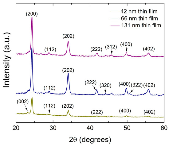
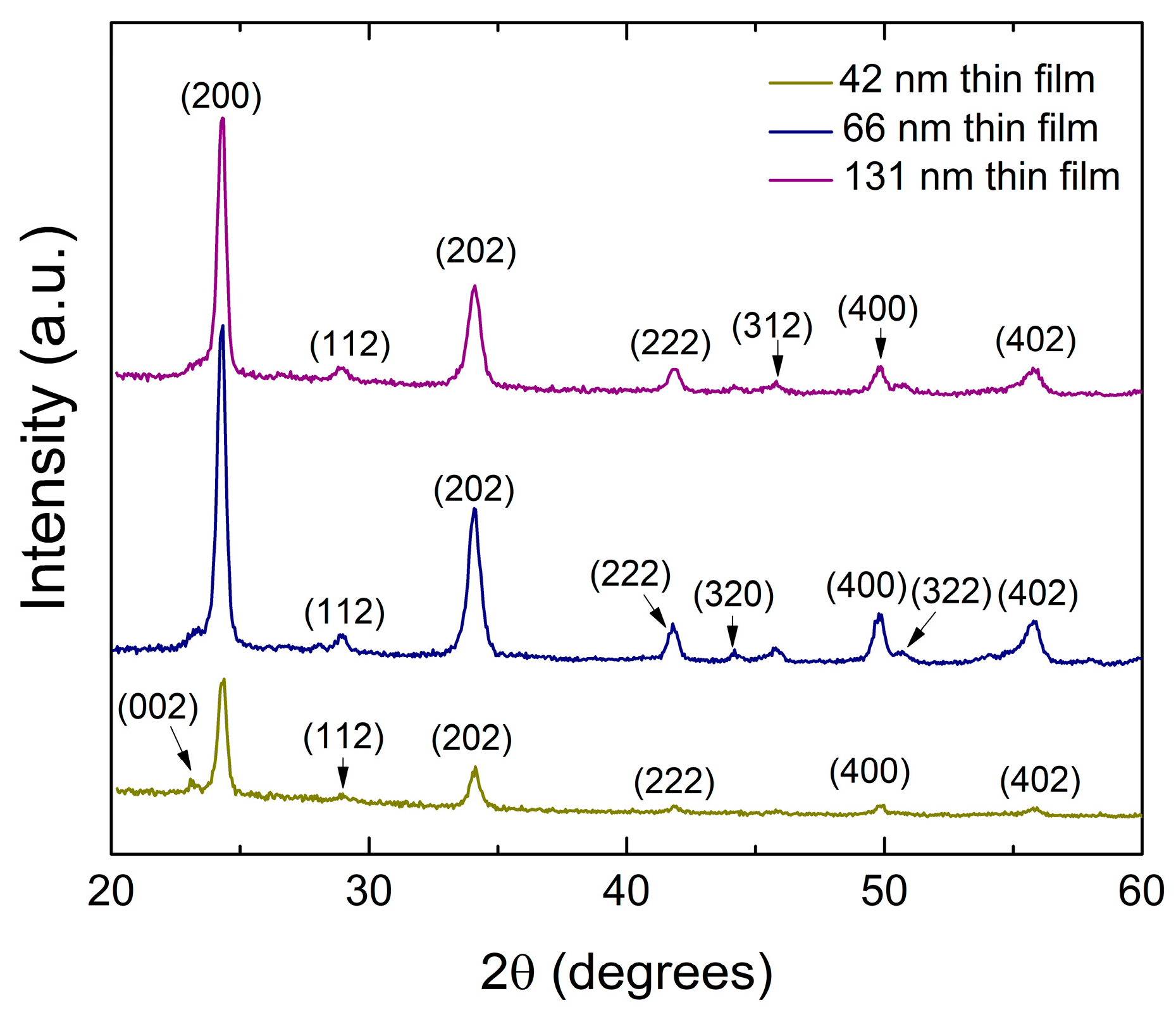
XRD of the annealed thin films reveal a clear thickness-dependent evolution of the crystalline structure of the WO3 thin films. All samples can be assigned to the monoclinic WO3 phase, see Figure 1, commonly indexed in the literature with the P21/n space group, No. 14 [19]. The most intense reflection in the films is indexed as (200), indicating a pronounced preferred orientation along the (200) plane. A marked increase in diffraction intensity and peak multiplicity is observed as the film thickness increases from 42 to 131 nm, indicating progressive crystallization and improved long-range structural order. The 42 nm film exhibits a weak and relatively broad diffraction feature near the low-angle WO3 reflections, suggesting limited crystallinity or very small coherent diffracting domains. In contrast, the 66 nm and especially the 131 nm films show sharper and more intense reflections, evidencing a substantial enhancement in crystalline quality with thickness. This trend agrees with previous sputtered WO3 studies showing that thicker films generally provide more favorable conditions for nucleation, grain growth, and crystallite alignment during post-deposition annealing [20]. From a structure-property standpoint, the thickness-dependent XRD evolution is important because, in WO3, crystallinity, preferred orientation, and defect chemistry are closely coupled to transport and sensing behavior. Reviews and mechanistic studies have emphasized that the electrical properties of WO3 are strongly affected by oxygen-vacancy-related donor states and by the atomic configuration of the exposed crystal planes. In particular, the literature has linked enhanced reactivity of WO3 surfaces to facet-dependent oxygen chemisorption and vacancy-mediated charge transfer, which means that the development of a stronger (200)-type texture may have direct implications for gas adsorption and resistance modulation. Therefore, the XRD results suggest that film thickness is not merely a geometric parameter, but a key variable controlling the crystalline order and preferred orientation that ultimately govern the functional response of WO3 thin films [11].
Figure 1.
X-ray diffraction patterns after annealing at 500 °C for the three different thicknesses of WO3 films.
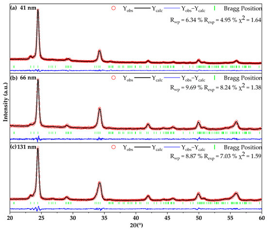
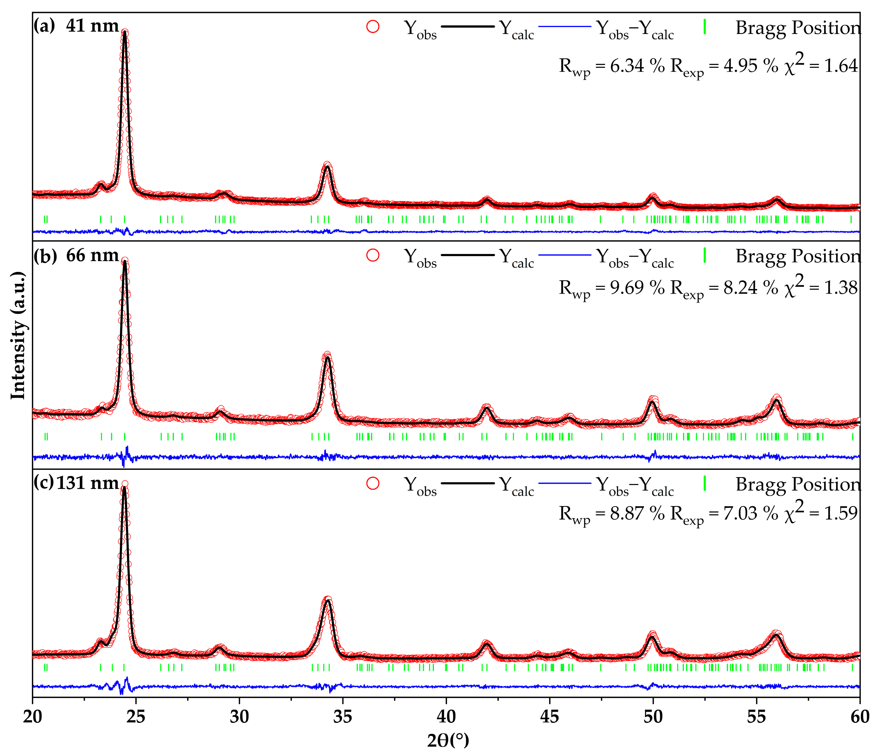
Structural characterization was performed by Rietveld refinement using the Thompson–Cox–Hastings pseudo-Voigt (TCH-pV) function implemented in the GSAS-II software [21]. The crystal structure model used as starting point for the refinement was the inorganic crystal structure database ICSD card No. 80056 [22]. The refinement strategy was carried out sequentially, starting with the scale factor and background, followed by correction of the instrumental zero shift. Subsequently, the unit-cell parameters were refined to properly match the Bragg positions. Once a satisfactory fit was obtained, the peak profile parameters, preferred orientation, asymmetry (if required), and atomic positions were refined in the final stage. The atomic displacement parameter (Uiso) was fixed during refinement in order to avoid over-parameterization and ensure refinement stability. The XRD Rietveld refinements are shown in Figure 2.
Figure 2.
Structural refinement for WO3 thin films of (a) 42 nm, (b) 66 nm and (c) 131 nm of thickness. Yobs is the observed XRD data measured, Ycalc is the structural model calculated by the refinement and Bragg-positions are vertical green lines.
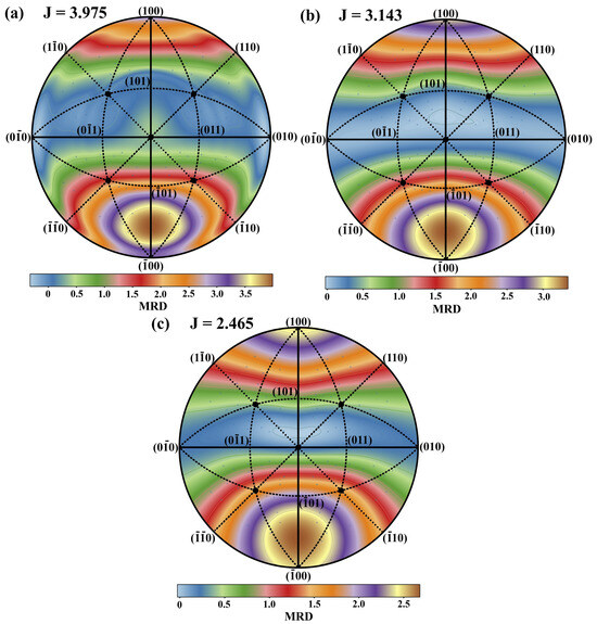
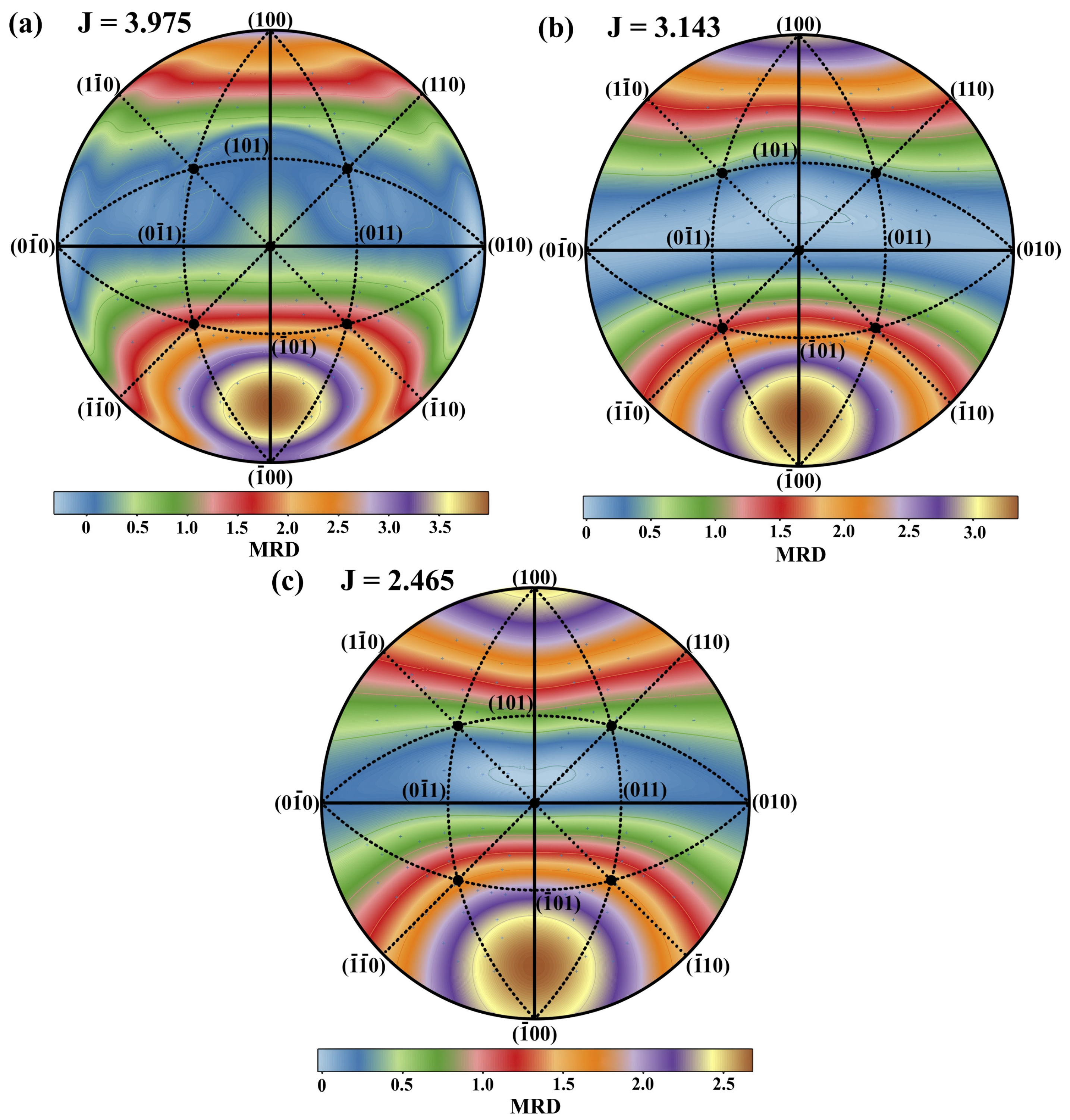
The agreement factors (Rwp and Rexp), the goodness of fit indicador (χ2), and the structural parameters calculated by the refinement of each thin film are compiled in the Table 1. It can be observed that the cell volume decreases as the thickness of the thin films increases. This behavior is well documented in metal oxides grown and particularly in WO3, which is not an intrinsic chemical effect of the material, instead a structural phenomenon associated with residual stresses, oxygen vacancies, interface effects, surface energy and structural relaxation. In reactive sputtering, thin films grow under conditions far from thermodynamic equilibrium. When the film thickness is very low, the film can be strongly influenced by the substrate, which may lead to an expansion of the unit cell. As the thickness increases, oxygen vacancies are reduced and a transition from W6+ to W5+ occurs, increasing the local effective ionic radius [23]. Additionally, distortions of the WO6 octahedra are generated, accompanied by enhanced structural densification and improved crystallinity [24,25,26,27,28]. The preferred orientation observed in reflection (200) was approximated in the Rietveld refinement using the spherical harmonics model [29,30] because it showed a better fit in approximating the experimental measurement compared to the March–Dollase method [31]. By using this model, it is possible to quantify the preferred orientation using the texture index J. For a random polycrystalline material, J = 1, while for textured polycrystalline materials, J > 1, if the material is monocrystalline, J = ∞ [29,30,32]. The refinement began with three coefficients (minimum number of coefficients for the P 21/n space group, No. 14) and was extended up to eight coefficients (harmonic order 4). Increasing the number of coefficients beyond this value did not significantly improve the fit and resulted in reduced convergence stability.
Table 1.
Lattice parameters, volume, atomic positions, and agreement factors for each Rietveld refinement.
Figure 3 shows the inverse pole figures (IPFs) for the thin films; the units are Multiple Random Distribution, MRD. Due to the monoclinic symmetry, the (200), (020), and (002) plane families are not symmetry-equivalent, as no operation interchanges the crystallographic axes. Consequently, the three thin films exhibit a concentration of the maximum MRD values associated with the (200) family (symmetrically distributed along planes (100) in the inverse pole figures). The progressive decrease of the texture index J with increasing film thickness suggests a reduction in preferential orientation. This behavior can be attributed to the influence reduction of the substrate during the film growth, which allows competitive grain development in multiple orientations and an increase in defect density, such as the possible rise in microstrains and the reduction in crystallite size, ultimately leading to a gradual weakening of the texture [33].
Figure 3.
Inverse pole figure for WO3 thin films of (a) 42 nm, (b) 66 nm and (c) 131 nm of thickness. Note: Non-central black dots indicate the (111) family of planes.
The volume-average crystallite size and microstrains was calculated using TCH-pV function in Fullprof Suite software. The ISizeModel and StrainModel parameters were set to 15 (monoclinic) and 2, respectively [21]. The selected models are consistent with the monoclinic Laue symmetry (2/m) [34,35]. Since the general methodology has been detailed in our previous work [36], only the parameters specific to the present study are described here. An anisotropic approximation was employed for both strain and crystallite size. The strain anisotropy was modeled through the refinement of S400, S040, S004, S220, S202, S022, S121, S301, and S103 strain parameters along with ξ, while the anisotropic apparent crystallite size was described using Y00, Y22+, Y22−, Y20, Y44+, Y44−, Y42+, Y42−, and Y40 coefficients along with IG parameter. Instrumental broadening was corrected by calibrating the resolution function (Res = 1) against a well-crystallized silicon standard, assuming a constant X-ray wavelength (λ), following the FullProf Suite manual guidelines.
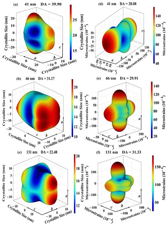
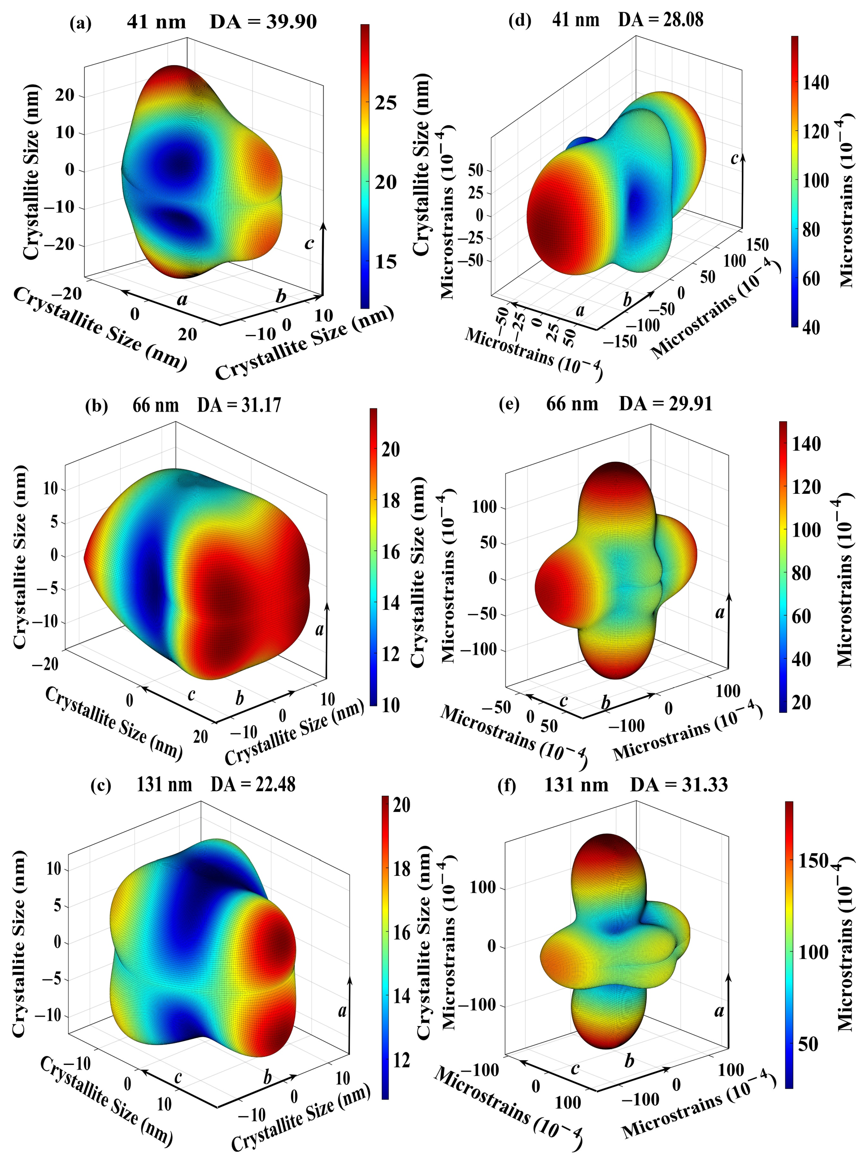
Table 2 shows the profile parameters refined and the microstructure parameters of the thin films. As previously suggested, the volume-average apparent crystallite size decreases from 18.64 nm for the 42 nm thin film to 14.45 nm for the 131 nm thin film due to the increase in defect density as can be seen in the progressive increase of the average maximum strain from 82.74 × 10⁻⁴ to 98.93 × 10⁻⁴.
Table 2.
Profile parameters refined (TCH-pV method) and microstructure parameters of the thin films.
In Figure 4 the spherical harmonics projections of both the volume-average apparent crystallite size and the average maximum strain for all thin films are shown. These projections were generated using MATLAB software (NM, United States), package R2023b version, processing the TCH-pV data refinement. The anisotropy degree (DA) quantifies the standard deviation of crystallite size and microstrain as a function of orientation in reciprocal space. A DA value equal to zero denotes an isotropic condition, where the directional distribution of both parameters can be represented by a spherical geometry in their corresponding graphical representations. In other way, increasing DA values reflect progressive deviations from this spherical symmetry, revealing orientation variations associated with different crystallographic directions. The evolution of the microstructural parameters with film thickness reveals two distinct tendencies. In one way, the volume-average apparent crystallite size slightly decreases from 18.64 nm to 14.45 nm as thickness increases and the DA associated with crystallite size exhibits a marked reduction. This behavior suggests a gradual homogenization in crystallite growth directions. In contrast, the average maximum microstrain increases with thickness, accompanied by a moderate rise in its DA. This indicates that although crystallite growth becomes more isotropic, internal microstrains intensify and become slightly more heterogeneously distributed in reciprocal space. Both behaviors are in accordance with the trend shown by the texture index J and support the explanation mentioned before.
Figure 4.
The spherical harmonics projection of three-dimensional bodies representing average apparent size for (a) 42 nm, (b) 66 nm, and (c) 131 nm thin films, and average maximum strain for (d) 42 nm, (e) 66 nm, (f) 131 nm WO3 thin films.
3.2. Morphology and Composition
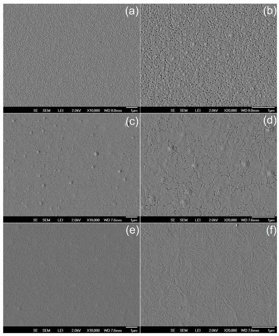
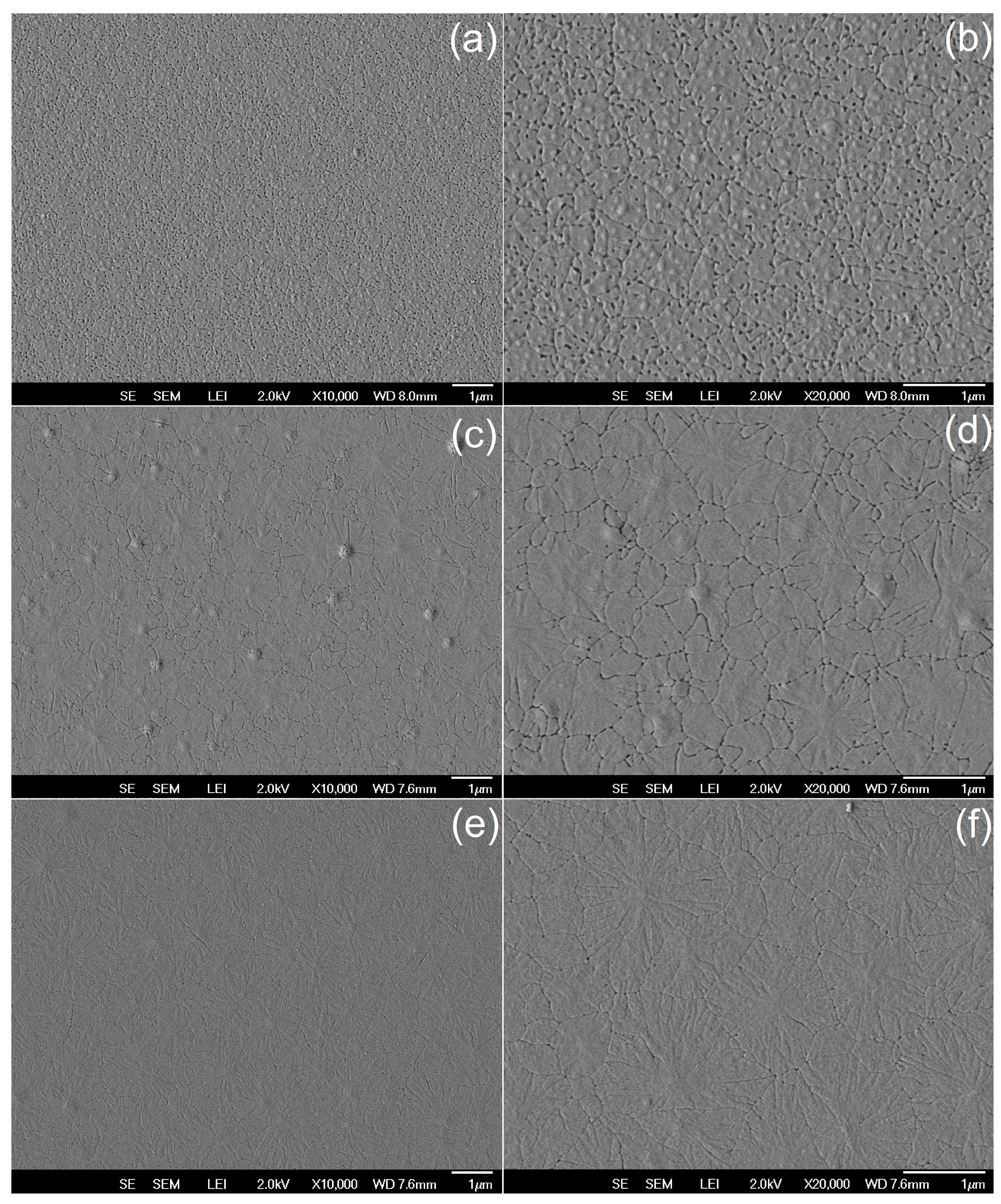
FE-SEM surface micrographs performed in secondary-electron mode reveals that the tungsten trioxide (WO3) thin films, after the crystallization heat treatment, exhibit a continuous surface characterized by an equiaxed granular morphology that appears to originate from central nucleation sites (Figure 5). The thinnest film (42 nm) presents smaller grains at the submicrometric scale (Figure 5a) together with a relatively high and homogeneously distributed surface porosity (Figure 5b). As the film thickness increases, this porosity progressively coalesces, as observed for the 66 nm film (Figure 5d), and becomes nearly absent in the thickest film (131 nm, Figure 5f), resulting in a gradual densification of the microstructure with increasing thickness. A clear grain growth is also evident, first in the 66 nm film (Figure 5c) and more prominently in the 131 nm film (Figure 5e). Despite these changes, well-defined grain boundaries are observed in all samples. In addition, very fine surface lines are visible on the grains, giving rise to a highly textured surface in the WO3 films. From the perspective of gas sensing, these microstructural features are particularly relevant. In resistive gas sensors based on metal-oxide semiconductors, such as WO3, the sensing mechanism is governed by the adsorption of oxidizing or reducing species on the surface and by the modulation of the potential barrier at grain boundaries due to the formation of an electron depletion layer [37]. Consequently, smaller grains and porous microstructures increase the specific surface area and the density of grain junctions, thereby enhancing the modulation of electrical resistance upon gas adsorption [38]. Previous studies have also shown that nanostructures exhibiting high surface roughness and porosity, such as nanoflakes and nanorods, can significantly enhance the response toward gases such as H2S and volatile organic compounds (VOCs), including acetaldehyde and xylene [39,40]. Therefore, parameters such as grain size, porosity, film thickness, and surface texture play a critical role in determining the sensitivity, response kinetics, and stability of WO3-based gas sensors, in agreement with the microstructural characteristics observed in the present films [41].
Figure 5.
FE-SEM surface micrographs of WO3 thin films with different thicknesses. Images correspond to the 42 nm film at (a) 10,000× and (b) 20,000× magnification; the 66 nm film at (c) 10,000× and (d) 20,000×; and the 131 nm film at (e) 10,000× and (f) 20,000×.
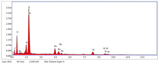
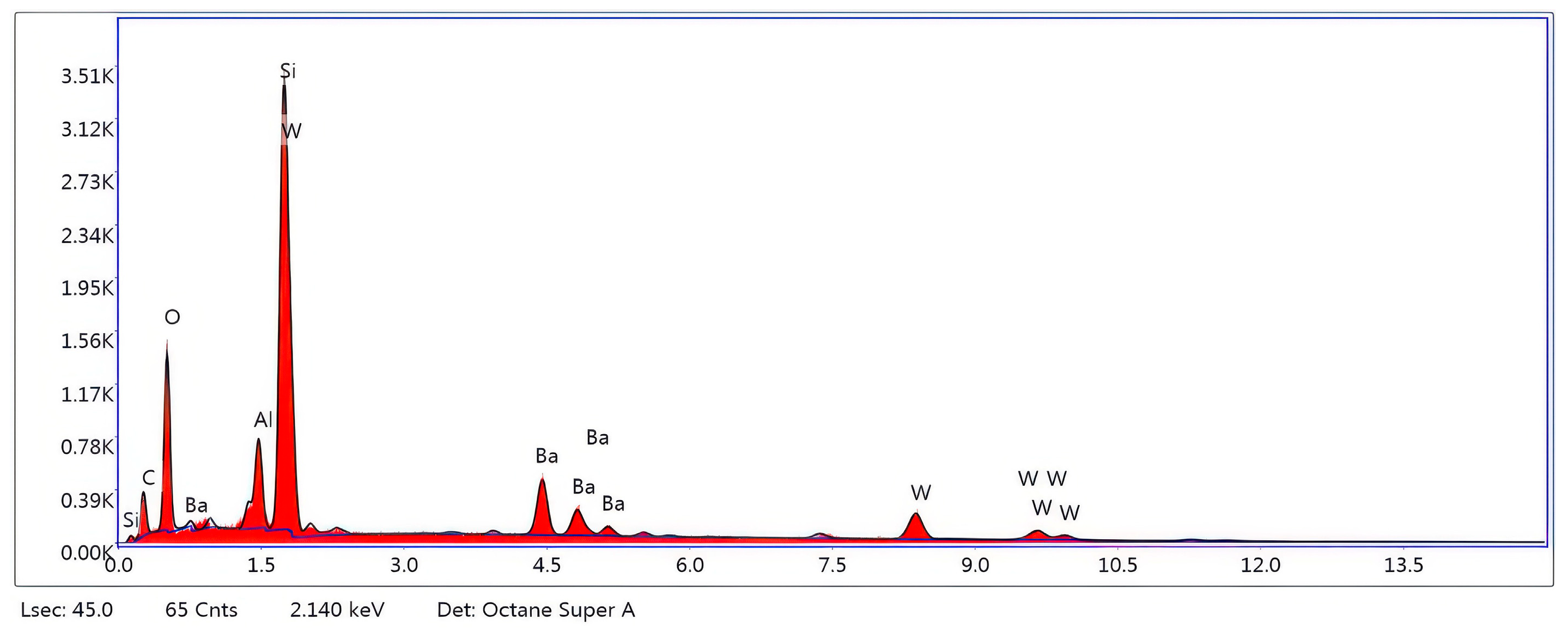
Figure 6 is an elemental analysis of the samples performed by energy dispersive X-ray spectroscopy (EDS) in general mode to corroborate the existence of tungsten trioxide. It can be seen that there are no contaminants or elements foreign to the tungsten oxide and elements related to the substrate.
Figure 6.
Elemental analysis of the samples performed by energy dispersive X-ray spectroscopy (EDS) on thin film of tungsten oxide.
3.3. CO2 Gas Response Characteristics
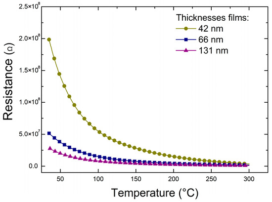
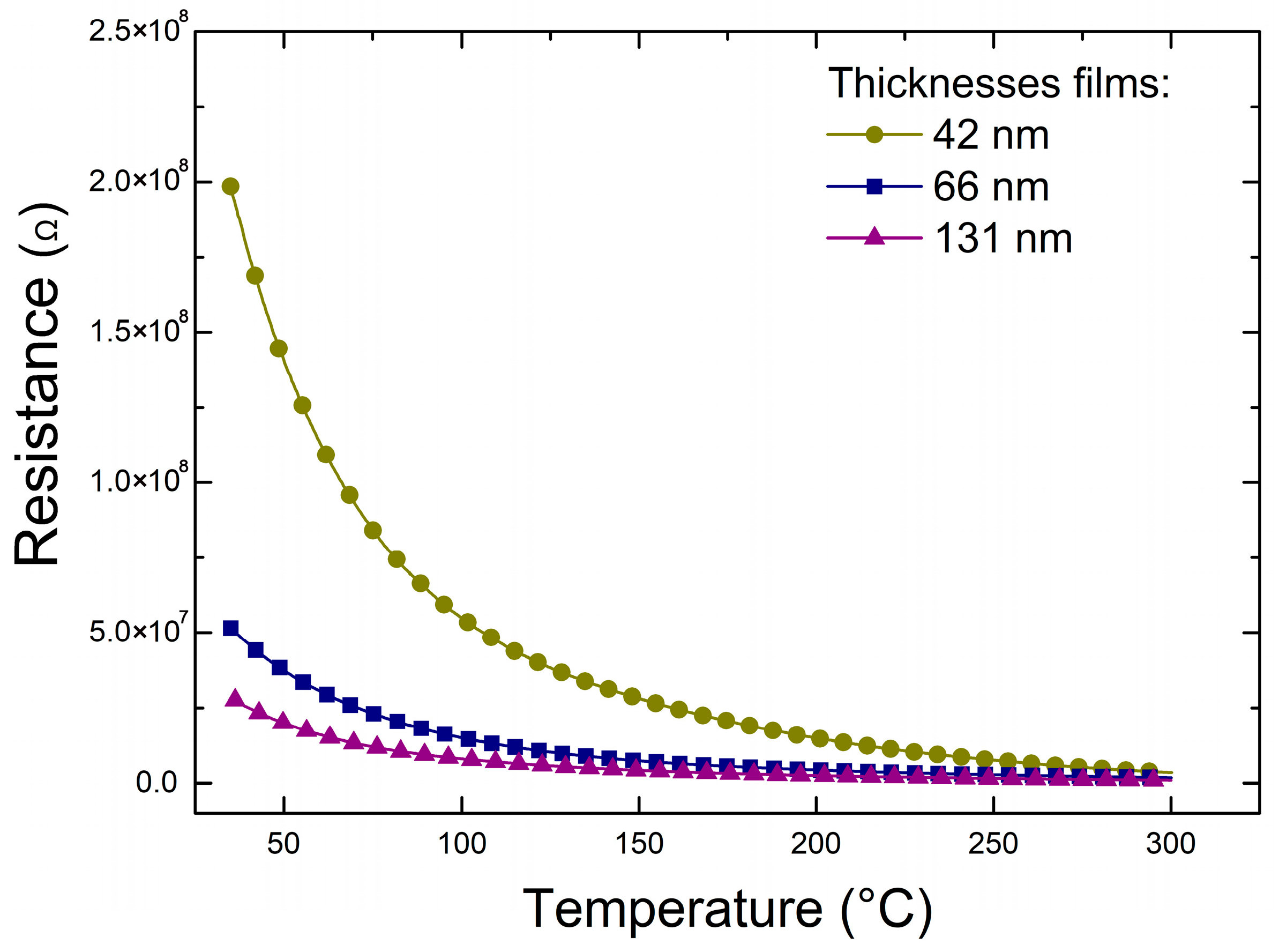
To analyze the semiconductor behavior of thin films grown with different thicknesses, the DC resistance was measured, revealing the drop in electrical resistance with increasing temperature, from room temperature to 300 °C. As shown in Figure 7, the thinner film has a higher resistance than the thicker film, which, according to Bhagwat [42], may be due to a higher concentration of oxygen vacancies that increases resistance.
Figure 7.
Semiconductor behavior of WO3 thin films.
The tungsten trioxide films CO2 gas detection mechanism, involves the interaction of gas molecules with the materials surface. This interaction results in a measurable response, such as a change in electrical conductivity [42]. To verify the existence of this detection mechanism in these tungsten trioxide films, a constant flow of extra-dry air was initially introduced into the Linkam chamber for a period prior to the introduction of the test gas. In these experiments, humidity measurements were taken using a Fluke 971 thermo-hygrometer. The relative humidity (RH) was maintained at 14% throughout all experiments and, therefore, under these relatively dry conditions, could limit the availability of OH− groups on the surface and interfere with the formation of bicarbonate (HCO3−) species, which in turn would weaken the interaction between CO2 molecules and the oxide surface [43], however, the formation of bicarbonates would result purely from the interaction of the CO2 gas with the WO3 material.
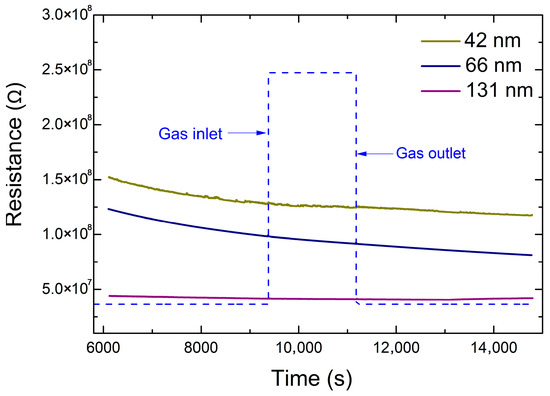
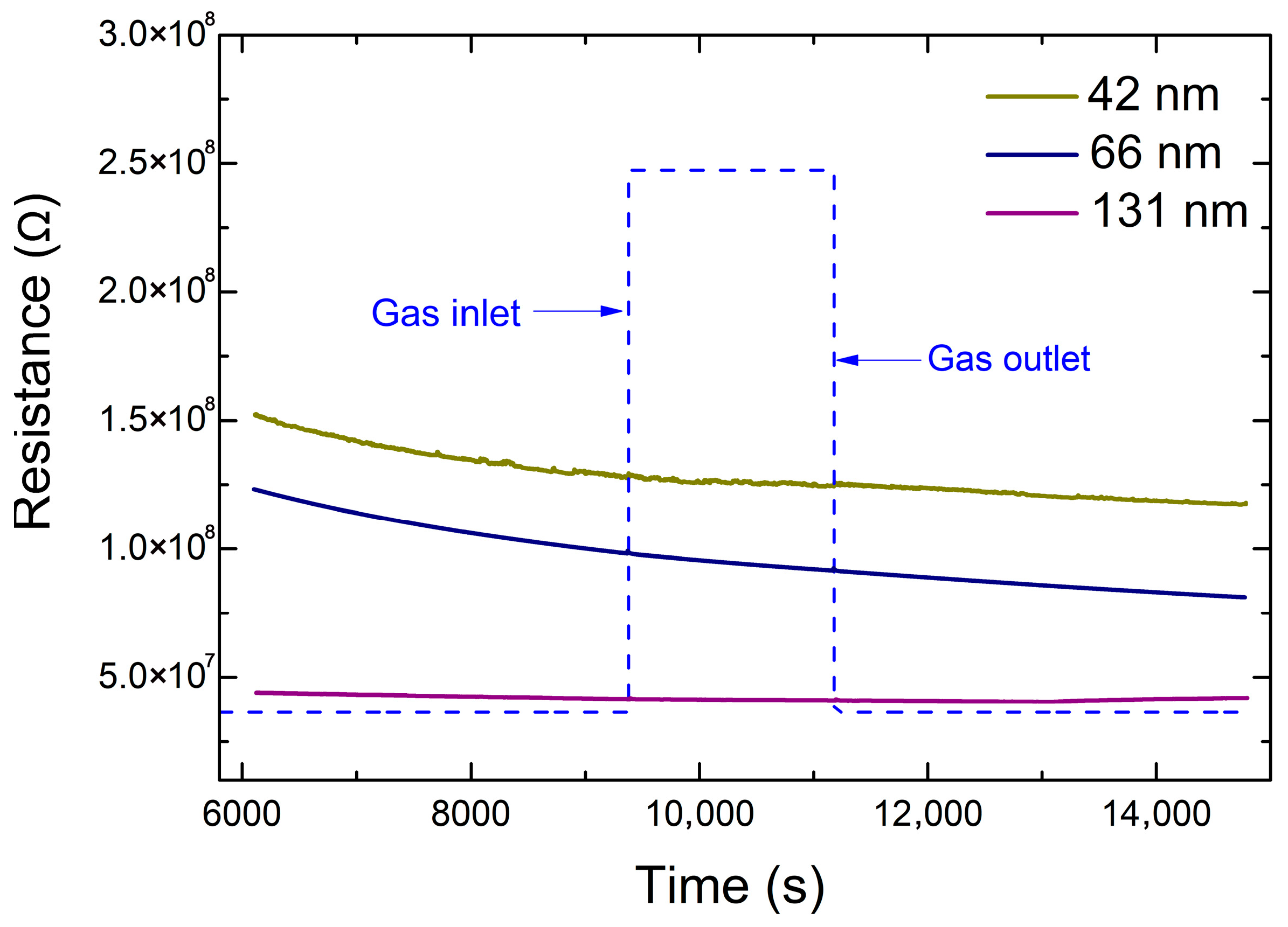
During the experiment, the electrical resistance was measured using tungsten probes placed on the thin films surface. After the selected time, the air was shut off, and then the gas flow containing 10,000 ppm (1%) carbon dioxide was introduced. Measurements were first taken at 150 °C, starting at a temperature slightly below that reported in the literature for this type of material, which detects other gases between 200 and 500 °C [44,45,46,47]. However, no signal was obtained at this temperature for any thickness of the thin films, see Figure 8. The interaction between CO2 gas and the different oxygen species present in the material depends largely on the operating temperature, as the concentration of free electrons due to charge exchange with the adsorbed gaseous species varies considerably [48].
Figure 8.
Electrical resistance measurement during CO2 sensitivity test measured at 150 °C for all film thicknesses.
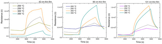
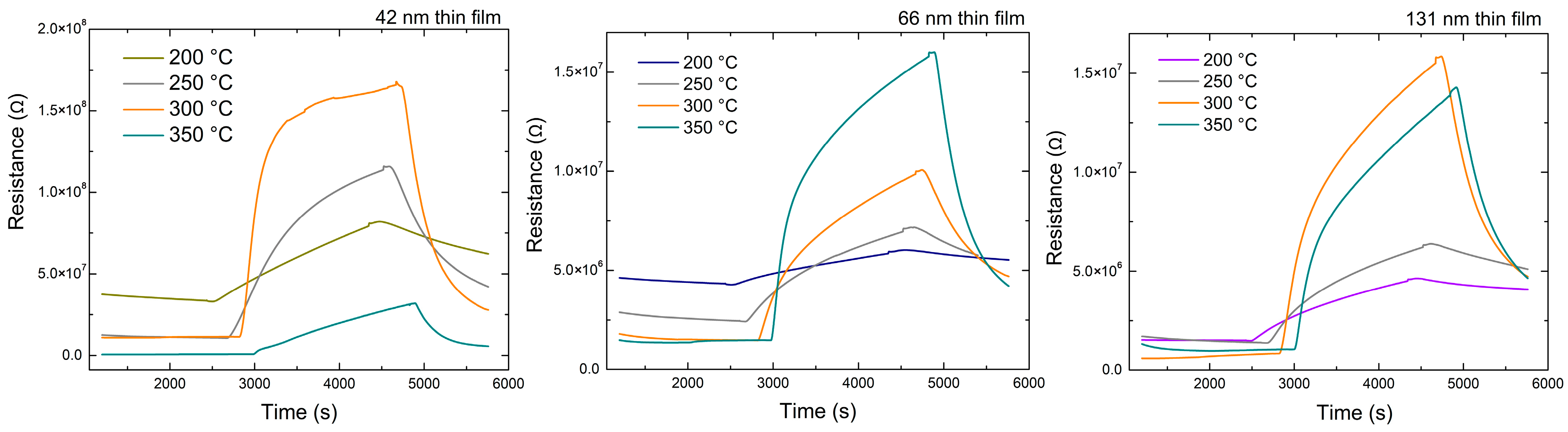
To evaluate whether the electrical resistance changed at other operating temperatures when the film was exposed to the target gas, measurements were conducted at 200, 250, 300, and 350 °C, see Figure 9. The gas-sensing mechanism of WO3 is governed by a chemiresistive process controlled by oxygen vacancies and adsorbed oxygen species. In air, O2 molecules chemisorb on the surface, extracting electrons from the conduction band and forming ionic species such as O2−, O−, and O2−. This process generates an electron-depletion layer near the surface and increases the resistance of the n-type WO3 semiconductor [49]. Upon exposure to reducing gases (e.g., CO, NH3), these species react with the adsorbed oxygen ions, releasing electrons back to the conduction band and thereby decreasing the resistance [50,51]. In contrast, for oxidizing gases such as NO2, additional adsorption results in further electron withdrawal from the semiconductor, leading to an increase in resistance, which is characteristic behavior for n-type metal-oxide sensors [52,53].
Figure 9.
CO2 gas response at temperatures from 200 °C to 350 °C.
In the case of CO2, which behaves as an oxidizing gas, the interaction occurs mainly with surface oxygen species or lattice oxygen from the WO3 crystals. CO2 can adsorb on the surface in both monodentate and bidentate configurations, forming carbonate species (CO32−) [54].
For each film thickness, an optimal response temperature was identified. For the 42 nm film, the response begins very clearly at 250 °C; however, the most pronounced increase is observed around 300 °C, where the resistance increase reaches its maximum value among the evaluated temperatures. This behavior can be explained by the favorable equilibrium between the adsorption of active oxygen species and the surface reaction kinetics at this temperature [54]. At 350 °C, the response decreases, which is consistent with the increase in the desorption rate of surface species typically observed in metal oxide sensors at elevated temperatures. Conversely, the 66 nm film exhibits the greatest resistance modulation at 350 °C. This result suggests that, for this thickness, the thermal activation of surface reactions and gas diffusion in the film’s porous network are more efficient at higher temperatures. In MOX sensors, film thickness influences gas diffusion and the relative contribution of depletion regions, which can shift the optimal operating temperature. For the 131 nm film, the behavior shows a significant response at both 300 °C and 350 °C. This could be related to the fact that in thicker films, electrical conduction involves multiple paths through the grains and grain boundaries. Therefore, the response depends not only on surface reaction but also on gas diffusion processes and the modulation of potential barriers at intergranular contacts. Overall, the results demonstrate that both operating temperature and film thickness significantly influence the sensor response, as they affect the adsorption-desorption equilibrium of oxygen species, surface reaction kinetics, and the modulation of depletion regions and intergranular potential barriers that govern charge transport in semiconducting metal oxide gas sensors.
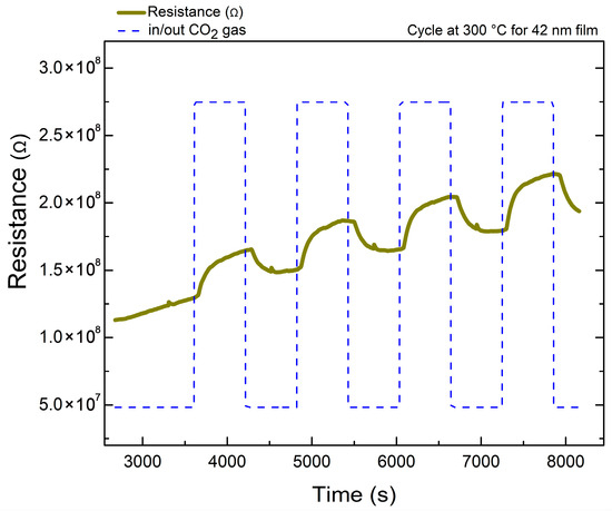
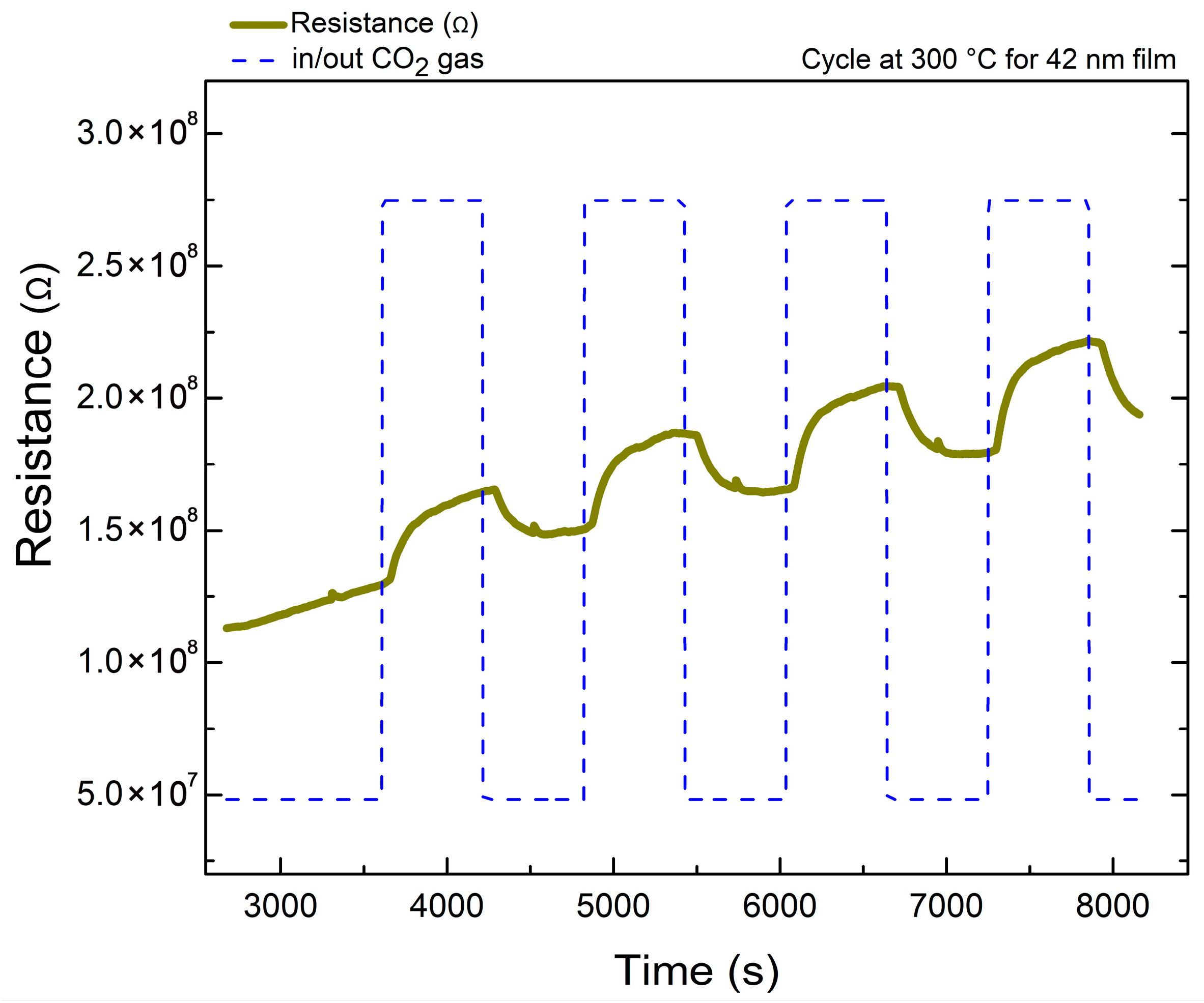
The dynamic sensing response stability was evaluated over a defined operating period. As a representative example, Figure 10 shows the behavior of a 42 nm tungsten trioxide (WO3) thin film operated at 300 °C during repeated exposure cycles to carbon dioxide (CO2). The resistance exhibits a clear and reproducible modulation associated with the alternating introduction and removal of CO2. During the gas exposure intervals, the electrical resistance progressively increases, while upon returning to the reference atmosphere, the resistance partially recovers to higher values. This behavior is consistent with the typical response of n-type metal oxide semiconductors, where surface interactions between adsorbed oxygen species and the target gas modify the electron concentration in the conduction band through charge transfer processes occurring in the surface depletion layer [55,56].
Figure 10.
CO2 gas cycles at 300 °C for the 42 nm WO3 thin film.
A notable feature of the response is the gradual upward shift of the reference resistance in successive detection cycles. The resistance increases from approximately 1.3 × 10⁸ Ω at the start of the experiment to values exceeding 2.0 × 10⁸ Ω in later stages, indicating a drift from the baseline. According to established models of defect chemistry for metal oxide gas sensors, this behavior can be attributed to the slow re-equilibration of intrinsic donor defects, particularly oxygen vacancies. In WO3 and other n-type metal oxides, oxygen vacancies act as electron donors, contributing to the material’s conductivity. Following high-temperature film growth and heat treatment, these defects can remain “frozen” at concentrations corresponding to temperatures above the actual operating conditions. During sensor operation at elevated temperatures, a gradual re-equilibration process occurs as oxygen diffuses into the oxide lattice, progressively reducing the concentration of oxygen vacancies and thus decreasing the free electron density in the conduction band. As a result, the electrical resistance of the film slowly increases over time. Despite this baseline shift, the periodic response associated with CO2 exposure remains clearly observable throughout the measurement. This indicates that the fundamental surface sensing mechanism remains active, while the long-term drift is governed primarily by bulk defect relaxation, rather than irreversible surface degradation. This behavior is consistent with previous observations in metal oxide semiconductor sensors, where slow oxygen diffusion and bulk defect equilibrium in the oxide produce gradual baseline shifts without completely suppressing the gas-induced response. Therefore, the results suggest that the sensing dynamics of the WO3 thin film arise from the interaction between surface adsorption processes that control the instantaneous response and the bulk defect chemistry that governs the long-term electrical stability of the device. One of the strategies reported in the literature to mitigate this phenomenon and reduce its impact on real-world applications is the implementation of prolonged thermal preconditioning or the incorporation of metallic dopants [55]. These approaches are currently being investigated in the present films, and the results will be reported in future work.
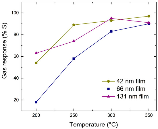
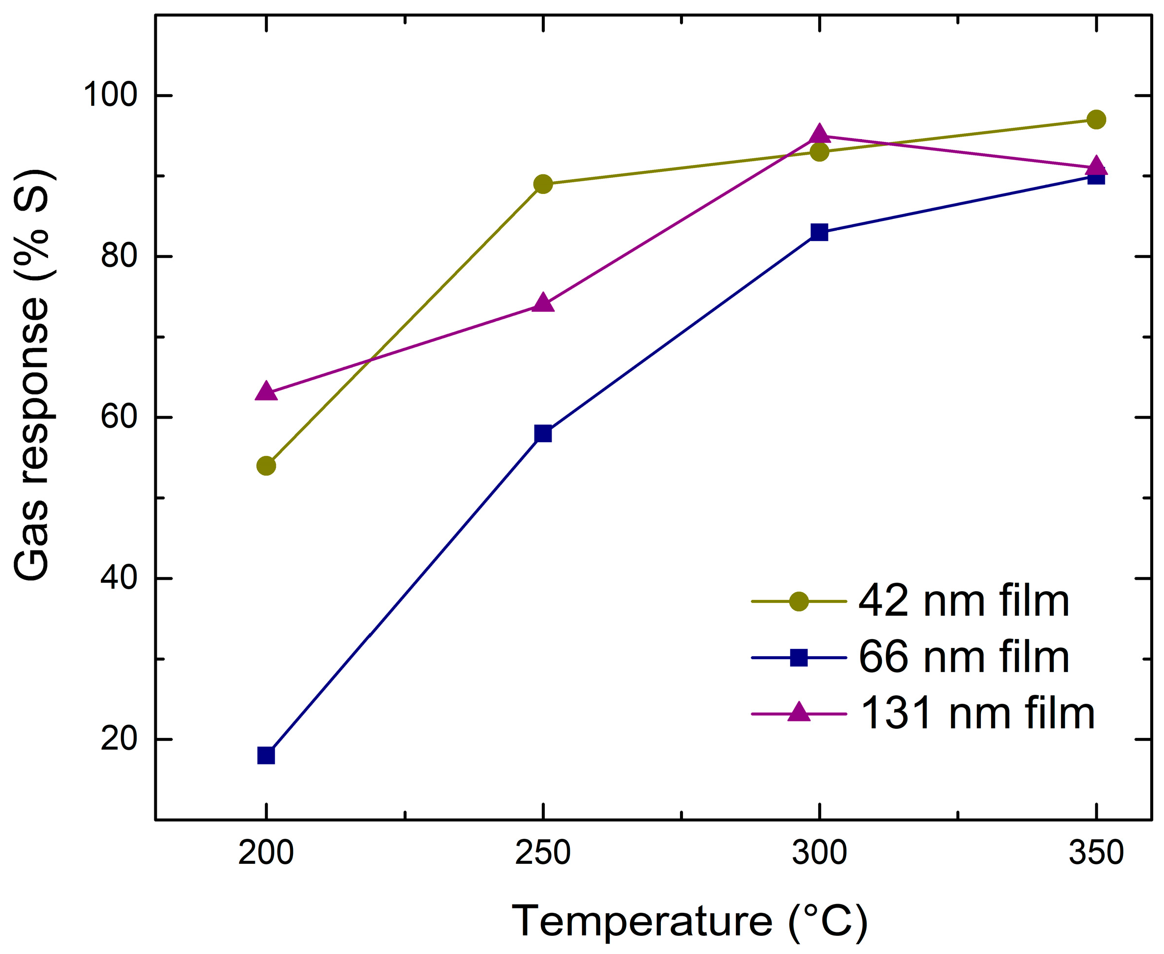
Figure 11 presents the resistance change in response to CO2 exposure, quantified as the sensitivity (%S) according to Equation (1), as a function of the operating temperature for the three WO3 thin films. In all cases, a general increase in sensor response is observed as the temperature rises from 200 °C to 350 °C, which is consistent with the typical behavior of metal oxide semiconductor gas sensors. This trend can be attributed to the enhanced thermal activation of adsorption–desorption processes and the increased mobility of charge carriers; however, the response does not exhibit a strictly linear dependence on temperature for all film thicknesses. For the thinnest film (42 nm), a high and stable response is observed within the 250–350 °C range, indicating efficient surface reactions under these conditions. In contrast, the 66 nm film appears to require higher thermal activation to reach an effective sensing regime, as evidenced by its more pronounced response at elevated temperatures. For the thickest film (131 nm), a higher degree of instability in sensitivity is observed, which may be associated with the combined effects of anisotropic surface reactivity and the formation of electronic barriers at grain boundaries. These factors can influence both the density and the nature of adsorption sites, thereby affecting the gas–surface interaction. As evidenced by the inverse pole figure analysis, the progressive decrease in the texture index (J) with increasing film thickness indicates a reduction in preferential crystallographic orientation, accompanied by a gradual weakening of the texture. This structural evolution may have a more significant impact on gas sensitivity than the concurrent decrease in crystallite size or the increase in microstrain, as it directly affects the surface reactivity and charge transport mechanisms governing the sensing response [57].
Figure 11.
Percentage sensitivity (%S) as a function of the operating temperature for three different thicknesses.
Table 3 summarizes the response and recovery times obtained during the evaluation of the sensitivity toward CO2 gas for each of the analyzed samples. The response time (t90) is commonly defined as the time required for the sensor signal to reach 90% of its steady-state value after gas exposure, while the recovery time corresponds to the time needed to return within 10% of the baseline after gas removal [18]. These parameters are widely used to describe the dynamic performance of MOX gas sensors, which typically exhibit response and recovery times ranging from seconds to minutes due to adsorption–desorption kinetics. To contextualize the results obtained in this work, representative approaches reported in the literature for the semiconductor metal oxide WO3 used in gas sensing are briefly discussed, Table 4. Pristine WO3 rarely exhibits significant gas-sensing performance near room temperature; instead, composites, heterostructures, and/or UV activation are typically employed to achieve faster responses, albeit often with moderate sensitivity. WO3 has been widely investigated for the detection of gases such as NO2, H2, and alcohols, whereas reports on CO2 sensing using this material remain scarce.
Table 3.
Response and recovery times obtained at the measured temperatures.
Table 4.
Overview of WO3 gas sensors: fabrication methods and sensing characteristics.
4. Discussion
The microstructural evolution of WO3 thin films with increasing thickness, from 42 to 131 nm, reveals a critical transition in transport and gas-sensing properties. Although the crystallite size slightly decreases (from 18.64 to 14.45 nm), the dominant factor governing CO2 sensitivity is the granular morphology and porosity. The 42 nm film exhibits a homogeneously distributed porous structure that maximizes the active surface area, thereby facilitating more efficient gas diffusion compared to the densified microstructure observed in the 131 nm film. The CO2 sensing mechanism for an oxidizing gas is associated with the formation of carbonate species (CO32−) on the surface, which extract electrons from the conduction band, leading to an increase in electrical resistance, as expected for an n-type semiconductor. The texture index (J) indicates that the 42 nm film exhibits the highest preferential orientation along the (200) plane, which has been correlated in the literature with a higher density of adsorption sites and reactive oxygen vacancies. The baseline drift observed during dynamic cycling (Figure 10) is attributed to the slow re-equilibration of intrinsic donor defects (oxygen vacancies) at the operating temperature (300 °C). This process is governed by bulk diffusion phenomena and does not compromise the instantaneous response capability of the sensor.
5. Conclusions
This study demonstrates that the thickness of WO3 thin films is a key control parameter that nonlinearly modulates CO2 sensitivity. It is concluded that the 42 nm film exhibits the best performance (sensitivity > 90% at 300 °C), which is attributed to the synergistic interplay between a grain size comparable to the Debye length and a high surface porosity. Thermal treatment at 500 °C effectively stabilizes the monoclinic P21/n phase, with a preferential (200) texture that enhances surface reactivity. The optimal operating temperature is found to lie between 300 °C and 350 °C, where the thermally activated adsorption/desorption processes of oxygen reach a dynamic equilibrium. These findings provide a clear pathway for the design of low-cost, high-efficiency CO2 sensors based on thickness engineering of WO3 thin films.
Author Contributions
Conceptualization, R.J.S.-H. and J.A.M.-A.; methodology, R.J.S.-H. and C.R.S.-R.; software, J.S.U.-C., C.R.S.-R. and M.C.G.-C.; validation, R.J.S.-H. and J.T.E.-G.; formal analysis, R.J.S.-H., J.S.U.-C. and G.M.H.-P.; investigation, R.J.S.-H., J.S.U.-C., C.R.S.-R. and M.C.G.-C.; resources, J.T.E.-G. and J.S.U.-C.; data curation, J.S.U.-C. and C.R.S.-R.; writing—original draft preparation, R.J.S.-H. and J.S.U.-C.; writing—review and editing, R.J.S.-H., J.S.U.-C. and G.M.H.-P.; visualization, C.R.S.-R., M.C.G.-C. and M.C.G.-C., supervision, J.A.M.-A., G.M.H.-P. and J.T.E.-G. All authors have read and agreed to the published version of the manuscript.
Funding
This research received no external funding.
Data Availability Statement
The data that support the findings of this study are available on request from the corresponding author, Renee Joselin Sáenz Hernández (joselin.saenz@cimav.edu.mx), due to protection of intellectual property and ongoing research.
Acknowledgments
The authors thank O. Solís-Canto, C. Leyva-Porras, A. Vázquez-Vargas, (NanoTech-CIMAV) for technical assistance provided for the realization of this work. During the preparation of this manuscript, the author(s) used ChatGPT (5.3 version) for the purposes of improving the readability and language of the manuscript. The authors have reviewed and edited the output and take full responsibility for the content of this publication.
Conflicts of Interest
The authors declare no conflicts of interest.
References
- Lin, Y.; Fan, Z. Compositing Strategies to Enhance the Performance of Chemiresistive CO2 Gas Sensors. Mater. Sci. Semicond. Process. 2020, 107, 104820. [Google Scholar] [CrossRef] [Scilit]
- Bhowmick, T.; Ghosh, A.; Nag, S.; Majumder, S.B. Sensitive and Selective CO2 Gas Sensor Based on CuO/ZnO Bilayer Thin-Film Architecture. J. Alloys Compd. 2022, 903, 163871. [Google Scholar] [CrossRef] [Scilit]
- Ghosh, A.; Zhang, C.; Shi, S.; Zhang, H. High Temperature CO2 Sensing and Its Cross-Sensitivity towards H2 and CO Gas Using Calcium Doped ZnO Thin Film Coated Langasite SAW Sensor. Sens. Actuators B Chem. 2019, 301, 126958. [Google Scholar] [CrossRef] [Scilit]
- Altun, B.; Karaduman Er, I.; Çağırtekin, A.O.; Ajjaq, A.; Sarf, F.; Acar, S. Effect of Cd Dopant on Structural, Optical and CO2 Gas Sensing Properties of ZnO Thin Film Sensors Fabricated by Chemical Bath Deposition Method. Appl. Phys. A Mater. Sci. Process. 2021, 127, 687. [Google Scholar] [CrossRef] [Scilit]
- Saruhan, B.; Lontio Fomekong, R.; Nahirniak, S. Review: Influences of Semiconductor Metal Oxide Properties on Gas Sensing Characteristics. Front. Sens. 2021, 2, 657931. [Google Scholar] [CrossRef] [Scilit]
- Zheng, H.; Ou, J.Z.; Strano, M.S.; Kaner, R.B.; Mitchell, A.; Kalantar-zadeh, K. Nanostructured Tungsten Oxide-Properties, Synthesis, and Applications. Adv. Funct. Mater. 2011, 21, 2175–2196. [Google Scholar] [CrossRef] [Scilit]
- Castro-Hurtado, I.; Tavera, T.; Yurrita, P.; Pérez, N.; Rodriguez, A.; Mandayo, G.G.; Castaño, E. Structural and Optical Properties of WO3 Sputtered Thin Films Nanostructured by Laser Interference Lithography. Appl. Surf. Sci. 2013, 276, 229–235. [Google Scholar] [CrossRef] [Scilit]
- Mukherjee, R.; Prajapati, C.S.; Sahay, P.P. Tailoring the Microstructural, Optical, and Electrical Properties of Nanocrystalline WO3 Thin Films Using Al Doping. J. Mater. Eng. Perform. 2014, 23, 3141–3151. [Google Scholar] [CrossRef] [Scilit]
- Mardare, C.C.; Hassel, A.W. Review on the Versatility of Tungsten Oxide Coatings. Phys. Status Solidi Appl. Mater. Sci. 2019, 216, 1900047. [Google Scholar] [CrossRef] [Scilit]
- Vemuri, R.S.; Carbjal-Franco, G.; Ferrer, D.A.; Engelhard, M.H.; Ramana, C.V. Physical Properties and Surface/Interface Analysis of Nanocrystalline WO3 Films Grown under Variable Oxygen Gas Flow Rates. Appl. Surf. Sci. 2012, 259, 172–177. [Google Scholar] [CrossRef] [Scilit]
- Epifani, M. Mechanistic Insights into WO3 Sensing and Related Perspectives. Sensors 2022, 22, 2247. [Google Scholar] [CrossRef] [Scilit]
- Dong, C.; Zhao, R.; Yao, L.; Ran, Y.; Zhang, X.; Wang, Y. A Review on WO3 Based Gas Sensors: Morphology Control and Enhanced Sensing Properties. J. Alloys Compd. 2020, 820, 153194. [Google Scholar] [CrossRef] [Scilit]
- Toby, B.H.; Von Dreele, R.B. GSAS-II: The Genesis of a Modern Open-Source All Purpose Crystallography Software Package. J. Appl. Crystallogr. 2013, 46, 544–549. [Google Scholar] [CrossRef] [Scilit]
- Rodríguez-Carvajal, J. Recent advances in magnetic structure determination by neutron powder diffraction. Phys. B Condens. Matter 1993, 192, 55–69. [Google Scholar] [CrossRef] [Scilit]
- González-Platas, J.; Rodríguez-Carvajal, J. GFourier: A Windows/Linux Program to Calculate and Display Fourier Maps; Program Available Within the FullProf Suite; Institut Laue-Langevin: Grenoble, France, 2007. [Google Scholar]
- Lu, Y.; Santino, L.M.; Acharya, S.; Anandarajah, H.; D’Arcy, J.M. Studying Electrical Conductivity Using a 3D Printed Four-Point Probe Station. J. Chem. Educ. 2017, 94, 950–955. [Google Scholar] [CrossRef] [Scilit]
- Mosavi, A.; Bertalan, B.; Imre, F.; Nadai, L.; Gorji, N.E. Electrical Characterization of CIGS Thin-Film Solar Cells by Two- and Four-Wire Probe Technique. Mod. Phys. Lett. B 2020, 34, 2050–2102. [Google Scholar] [CrossRef] [Scilit]
- Ahsan, M. Thermally Evaporated Tungsten Oxide (WO3) Thin Films for Gas Sensing Applications. Ph.D. Thesis, Queensland University of Technology, Brisbane, Australia, 2012. [Google Scholar]
- Alina, A.K.; Kadyrzhanov, K.K.; Kozlovskiy, A.A.; Konuhova, M.; Popov, A.I.; Shlimas, D.D.; Borgekov, D.B. WO3/ZnWO4 Microcomposites with Potential Application in Photocatalysis. Opt. Mater. 2024, 150, 115280. [Google Scholar] [CrossRef] [Scilit]
- Mohamedkhair, A.K.; Drmosh, Q.A.; Qamar, M.; Yamani, Z.H. Tuning Structural Properties of WO3 Thin Films for Photoelectrocatalytic Water Oxidation. Catalysts 2021, 11, 381. [Google Scholar] [CrossRef] [Scilit]
- Cox, D.E.; Hastings, J.B.; Cardoso, L.P.; Finger, L.W. Synchrotron X-Ray Powder Diffraction at X13A: A Dedicated Powder Diffractometer at the National Synchrotron Light Source. Mater. Sci. Forum 1986, 9, 1–20. [Google Scholar] [CrossRef] [Scilit]
- Woodward, P.M.; Sleight, A.W.; Vogt, T. Structure Refinement of Triclinic Tungsten Trioxide. J. Phys. Chem. Solids 1995, 56, 1305–1315. [Google Scholar] [CrossRef] [Scilit]
- Sáenz-Hernández, R.J.; Herrera-Pérez, G.M.; Uribe-Chavira, J.S.; Grijalva-Castillo, M.C.; Elizalde-Galindo, J.T.; Matutes-Aquino, J.A. Correlation Between Thickness and Optical Properties in Nanocrystalline γ-Monoclinic WO3 Thin Films. Coatings 2022, 12, 1727. [Google Scholar] [CrossRef] [Scilit]
- Ohring, M. Materials Science of Thin Films, 2nd ed.; Academic Press: New York, NY, USA, 2002; ISBN 9780125249751. [Google Scholar]
- Tomaev, V.V.; Sokhovich, E.V.; Myakin, S.V.; Polishchuk, V.A.; Semenova, A.A. Obtaining and Studying Films of Tungsten, Titanium and Their Oxides. Glass Phys. Chem. 2022, 48, 61–68. [Google Scholar] [CrossRef] [Scilit]
- Shi, Y.; Liu, T.; Hu, R.; Xu, H.; Yang, C.; Yang, L.; Feng, L.; Jiang, X. Synergy of W Doping and Oxygen Vacancy Engineering on D-Band Center Modulation for Enhanced Gas Sensing Performance. J. Mater. Chem. A 2024, 12, 4770–4781. [Google Scholar] [CrossRef] [Scilit]
- Li, J.; Na, E.; Liang, X.; Liang, Q.; Fan, M.; Chen, H.; Li, G.-D.; Zou, X. Surface Oxygen Chemistry of Metal Oxide Semiconductors for Gas-Sensing Applications. Inorg. Chem. Front. 2024, 11, 8602–8626. [Google Scholar] [CrossRef] [Scilit]
- Gudmundsson, J.T.; Anders, A.; von Keudell, A. Foundations of Physical Vapor Deposition with Plasma Assistance. Plasma Sources Sci. Technol. 2022, 31, 083001. [Google Scholar] [CrossRef] [Scilit]
- Bunge, H.-J. Texture Analysis in Materials Science: Mathematical Methods; Butterworths: London, UK, 1969. [Google Scholar] [CrossRef] [Scilit]
- Von Dreele, R. Quantitative Texture Analysis by Rietveld Refinement. J. Appl. Crystallogr. 1997, 30, 517–525. [Google Scholar] [CrossRef] [Scilit]
- Sitepu, H.; O’Connor, B.H.; Li, D. Comparative Evaluation of the March and Generalized Spherical Harmonic Preferred Orientation Models Using X-Ray Diffraction Data for Molybdite and Calcite Powders. J. Appl. Crystallogr. 2005, 38, 158–167. [Google Scholar] [CrossRef] [Scilit]
- Larson, A.; Von Dreele, R.B. General Structure Analysis System (GSAS); Los Alamos National Laboratory: Los Alamos, NM, USA, 2000.
- Birkholz, H. Thin Film Analysis by X-Ray Scattering; Wiley-VCH: Weinheim, Germany, 2006; ISBN 978-3-527-31052-4. [Google Scholar]
- Popa, N.C. The (Hkl) Dependence of Diffraction-Line Broadening Caused by Strain and Size for All Laue Groups in Rietveld Refinement. J. Appl. Cryst. 1998, 31, 176. [Google Scholar] [CrossRef] [Scilit]
- Stephens, P.W. Phenomenological Model of Anisotropic Peak Broadening in Powder Diffraction. J. Appl. Cryst. 1999, 32, 281. [Google Scholar] [CrossRef] [Scilit]
- Uribe-Chavira, J.S.; Herrera-Pérez, G.; Santillán-Rodríguez, C.R.; Sáenz-Hernández, R.J.; Matutes-Aquino, J.A.; Grijalva-Castillo, M.C. X-Ray Diffraction Analysis by Rietveld Refinement of FeAl Alloys Doped with Terbium and Its Correlation with Magnetostriction. J. Rare Earths 2023, 41, 1217–1224. [Google Scholar] [CrossRef] [Scilit]
- Korotcenkov, G. Metal Oxides for Solid-State Gas Sensors: What Determines Our Choice? Mater. Sci. Eng. B 2007, 139, 1–23. [Google Scholar] [CrossRef] [Scilit]
- Li, X.; Fu, L.; Karimi-Maleh, H.; Chen, F.; Zhao, S. Innovations in WO3 Gas Sensors: Nanostructure Engineering, Functionalization, and Future Perspectives. Heliyon 2024, 10, e27740. [Google Scholar] [CrossRef] [Scilit]
- Oros, C.; Sangpradub, P.; Daunglaor, P.; Yodsawad, T. Oxygen Plasma Treatment WO3 Nanorods for Improvement H2S Gas Sensing. J. Mater. Sci. Appl. Energy 2024, 13, 248329. [Google Scholar] [CrossRef] [Scilit]
- Fasquelle, D.; Verbrugghe, N.; Députier, S. Tungsten-Based Cost-Effective Gas Sensors for H2S Detection. Chemosensors 2021, 9, 295. [Google Scholar] [CrossRef] [Scilit]
- Modak, M.; Rane, S.; Jagtap, S. WO3: A Review of Synthesis Techniques, Nanocomposite Materials and Their Morphological Effects for Gas Sensing Application. Bull. Mater. Sci. 2023, 46, 28. [Google Scholar] [CrossRef] [Scilit]
- Godbole, R.; Godbole, V.P.; Alegaonkar, P.S.; Bhagwat, S. Effect of Film Thickness on Gas Sensing Properties of Sprayed WO3 Thin Films. New J. Chem. 2017, 41, 11807–11816. [Google Scholar] [CrossRef] [Scilit]
- Vázquez-Vargas, D.A.; Pizá-Ruiz, P.; Solís-Canto, O.; Sáenz-Hernández, R.J.; Amézaga-Madrid, P. Low-Temperature CO2 Sensing Performance of Pt-Decorated ZnO and NiO Thin Films: Synthesis and Characterization. Phys. B Condens. Matter 2025, 717, 417860. [Google Scholar] [CrossRef] [Scilit]
- Castañeda-Aviña, L. Gas Sensors Based on Semiconductors. Rev. Int. Investig. Innov. Technol. 2018, 33, 1–16. [Google Scholar]
- Xie, G.; Yu, J.; Chen, X.; Jiang, Y. Gas Sensing Characteristics of WO3 Vacuum Deposited Thin Films. Sens. Actuators B Chem. 2007, 123, 909–914. [Google Scholar] [CrossRef] [Scilit]
- Galatsis, K.; Li, Y.; Wlodarski, W.; Kalantar-zadeh, K. Sol–Gel Prepared MoO3–WO3 Thin-Films for O2 Gas Sensing. Sens. Actuators B Chem. 2001, 77, 478–483. [Google Scholar] [CrossRef] [Scilit]
- Ahsan, M.; Tesfamichael, T.; Ionescu, M.; Bell, J.; Motta, N. Low Temperature CO Sensitive Nanostructured WO3 Thin Films Doped with Fe. Sens. Actuators B Chem. 2012, 162, 14–21. [Google Scholar] [CrossRef] [Scilit]
- Ciftyurek, E.; Li, Z.; Schierbaum, K. Adsorbed Oxygen Ions and Oxygen Vacancies: Their Concentration and Distribution in Metal Oxide Chemical Sensors and Influencing Role in Sensitivity and Sensing Mechanisms. Sensors 2023, 23, 29. [Google Scholar] [CrossRef] [Scilit]
- Dey, A. Semiconductor Metal Oxide Gas Sensors: A Review. Mater. Sci. Eng. B 2018, 229, 206–217. [Google Scholar] [CrossRef] [Scilit]
- Jung, G.; Hong, S.; Jeong, Y.; Shin, W.; Park, J.; Kim, D.; Lee, J.H. Highly Selective and Low-Power Carbon Monoxide Gas Sensor Based on the Chain Reaction of Oxygen and Carbon Monoxide to WO3. ACS Appl. Mater. Interfaces 2022, 14, 17950–17958. [Google Scholar] [CrossRef] [Scilit]
- Xue, L.; Zhang, F.; Dang, J.; Zhang, Y.; Li, X.; Liu, T.; Wang, Q. Room-Temperature NH3 Sensor with Ppb Detection via AACVD of Nanosphere WO3 on IO SnO2. Ceram. Int. 2024, 50, 47991–47999. [Google Scholar] [CrossRef] [Scilit]
- Kanchan Kumar, D.; Bharathi, P.; Archana, J.; Navaneethan, M.; Harish, S. Optimizing NO2 Gas Sensor Performance: Investigating the Influence of Cobalt Doping on WO3 Recovery Kinetics for Enhanced Gas Sensing Application. Sens. Actuators B Chem. 2024, 421, 136477. [Google Scholar] [CrossRef] [Scilit]
- Mathankumar, G.; Bharathi, P.; M. Mohan, K.; Archana, J.; Harish, S.; Navaneethan, M. Defect Manipulation of WO3 Nanostructures by Yttrium for Ultra-Sensitive and Highly Selective NO2 Detection. Sens. Actuators B Chem. 2022, 353, 131057. [Google Scholar] [CrossRef] [Scilit]
- Lozano-Rosas, R.; Lamas, D.G.; Sánchez-Ochoa, F.; Cocoletzi, G.H.; Karthik, T.V.K.; Robles-Águila, M.J. CO2 Sensing Properties of WO3 Powder: Experimental and Theoretical Studies. Appl. Phys. A Mater. Sci. Process. 2021, 127, 815. [Google Scholar] [CrossRef] [Scilit]
- Müller, G.; Sberveglieri, G. Origin of Baseline Drift in Metal Oxide Gas Sensors: Effects of Bulk Equilibration. Chemosensors 2022, 10, 171. [Google Scholar] [CrossRef] [Scilit]
- Šutka, A.; Zubkins, M.; Linarts, A.; Lapčinskis, L.; MalNieks, K.; Verners, O.; Sarakovskis, A.; Grzibovskis, R.; Gabrusenoks, J.; Strods, E.; et al. Tribovoltaic Device Based on the W/WO3 Schottky Junction Operating through Hot Carrier Extraction. J. Phys. Chem. C 2021, 125, 14212–14220. [Google Scholar] [CrossRef] [Scilit]
- Kwong, W.L.; Koshy, P.; Hart, J.N.; Xu, W.; Sorrell, C.C. Critical Role of {002} Preferred Orientation on Electronic Band Structure of Electrodeposited Monoclinic WO3 Thin Films. Sustain. Energy Fuels 2018, 2, 2224–2236. [Google Scholar] [CrossRef] [Scilit]
- Singh, S.; Gurawal, P.; Malik, G.; Adalati, R.; Kaur, D.; Chandra, R. Highly Responsive and Selective NO Gas Sensing Based on Room Temperature Sputtered Nanocrystalline WO3/Si Thin Films. Micro Nanostruct. 2024, 188, 207794. [Google Scholar] [CrossRef] [Scilit]
- Lei, G.; Li, Z.; Lu, G.; Hu, J.; Shang, H.; Zhang, X.; Liu, X.; Zhang, J.; Guo, X. Tungsten Oxide Thin Films for Highly Sensitive Triethylamine Detection. J. Mater. 2022, 8, 408–416. [Google Scholar] [CrossRef] [Scilit]
- Kim, T.H.; Hasani, A.; Van Quyet, L.; Kim, Y.; Park, S.Y.; Lee, M.G.; Sohn, W.; Nguyen, T.P.; Choi, K.S.; Kim, S.Y.; et al. NO2 Sensing Properties of Porous Au-Incorporated Tungsten Oxide Thin Films Prepared by Solution Process. Sens. Actuators B Chem. 2019, 286, 512–520. [Google Scholar] [CrossRef] [Scilit]
- Ramya Barathy, T.; Yadav, P.V.K.; Mondal, A.; Ramakrishnan, K.; Jarugala, J.; Liu, C.; Reddy, Y.A.K. Enhanced Response of WO3 Thin Film Through Ag Loading towards Room Temperature Hydrogen Gas Sensor. Chemosphere 2024, 353, 141545. [Google Scholar] [CrossRef] [Scilit]
- Nalimova, S.S.; Shomakhov, Z.V.; Zyryanova, O.D.; Kondratev, V.M.; Bui, C.D.; Gurin, S.A.; Moshnikov, V.A.; Zhilenkov, A.A. WO3−x/WS2 Nanocomposites for Fast-Response Room Temperature Gas Sensing. Molecules 2025, 30, 566. [Google Scholar] [CrossRef] [Scilit] [PubMed]
- Ramola, R.C.; Negi, S.; Rawat, M.; Singh, R.C.; Singh, F. Annealing Effects on Gas Sensing Response of Ga-Doped ZnO Thin Films. ACS Omega 2021, 6, 11660–11668. [Google Scholar] [CrossRef] [Scilit] [PubMed]

Disclaimer/Publisher’s Note: The statements, opinions and data contained in all publications are solely those of the individual author(s) and contributor(s) and not of MDPI and/or the editor(s). MDPI and/or the editor(s) disclaim responsibility for any injury to people or property resulting from any ideas, methods, instructions or products referred to in the content. |
© 2026 by the authors. Licensee MDPI, Basel, Switzerland. This article is an open access article distributed under the terms and conditions of the Creative Commons Attribution (CC BY) license.