


Abstract
The efficiency of perovskite solar cells (PSCs) is mainly determined by their electron transport layer (ETL). In this work, we present a facile and efficient strategy to incorporate iminodiacetic acid (IDA) as a cost-effective, multifunctional dopant into hydrothermally synthesized TiO2 ETLs. This modification enables holistic defect passivation in the bulk TiO2, on its surface, and at the TiO2/perovskite interface, thereby significantly improving device performance. In particular, the dicarboxyl groups (-COOH) of the IDA molecule coordinate with Ti ions and oxygen vacancies at the TiO2 surface, effectively passivate the deep level traps, and improve the carrier (electron) mobility. At the same time, the imino groups (-NH-) assist in forming a thick and highly crystalline CsPbI3−xBrx perovskite film by coordinating to free Pb2+. Consequently, the best-performing device (5 mg/mL IDA) achieves a peak PCE of 12.16%, representing a relative enhancement of 38.9% compared to the control device (8.78%). The modified devices show significantly lower hysteresis (from 0.172 to 0.055) and better stability with more than 82% retention in the original performance after being stored in ambient air (25–30 °C, 20–30% RH) for 60 days. The present study offers a low-cost and industrially compatible technological pathway to produce efficient inorganic PSCs through molecular interfacial engineering.
1. Introduction
In the field of photovoltaics, thanks to their outstanding light-harvesting ability, PSCs have realized an unprecedented breakthrough on PCE, solution processability, and low cost. Since their first report in 2009, the certified PCE of PSCs soared from the beginning of 3.9% to 27.14% at the end of 2024 [1,2], showing tremendous promise for industrial use. Underlying this milestone achievement is the synergistic optimization of the whole device architecture, amongst which the fabrication of high-performance perovskite light-harvesting layers and the interfacial engineering of the ETL and hole transport layer (HTL) are regarded as pivotal determinants for improving the optoelectronic performances of devices [3]. In the case of n-i-p structure PSCs, in addition to being a deposition platform for perovskites, an efficient ETL is responsible for electron extraction and transport and blocking holes to suppress recombination [4]. Its behavior determines the charge transport efficiency, interfacial compatibility, and long-term stability of the device, thus becoming one of the main research topics in device structure design. Among various ETL materials, TiO2 has become one of the most widely utilized ETL materials in normal-architecture PSCs. This is attributed to its prominent advantages such as scalable solution-processable fabrication, low cost, and outstanding chemical stability [5,6], coupled with its well-matched conduction band energy level with that of inorganic perovskite materials, which ensures the efficient extraction and transport of photogenerated electrons [7].
Although TiO2 is widely adopted as an electron transport layer (ETL) in perovskite solar cells (PSCs) owing to its favorable energy alignment, high electron mobility, and solution processability, TiO2 films fabricated via conventional solution-based methods suffer from several intrinsic limitations—including low crystallinity, high defect density, and poor interfacial contact—that collectively impede further efficiency enhancement and hinder commercial scalability. Firstly, the inherently low electron mobility in TiO2 results in the hindered transport of photogenerated electrons both within the ETL and at the ETL/perovskite interface, easily inducing charge accumulation [8,9]. Second, the nanoparticles in the TiO2 precursor solution have a tendency to aggregate, leading to the formation of numerous defects including pinholes and grain boundaries in the prepared films; these defects will lead to the direct contact of the perovskite layer with FTO conductive substrate creating leakage pathways that aggravate interfacial carrier recombination and impede charge transport efficiency. More importantly, the solution-based synthesis will unavoidably generate surficial defects like oxygen vacancies, which are deep-level traps, and they greatly hinder carrier transportation, promote nonradiative recombination, and induce interfacial charge accumulation, which finally leads to a drop in open-circuit voltage (Voc), intensification of the hysteresis effect, and the loss of the long-term stability of the device [10,11].
To address the above problems, many researchers have proposed various methods for modifying the TiO2 ETL, such as elemental doping, interfacial modification, microstructure optimization, and molecular interface engineering in order to enhance device performance by controlling the electron transport properties, defect state density, and interfacial compatibility of the ETL [12]. One effective strategy is elemental doping (using metal or non-metal ions) to modulate the electronic structure and improve the conductivity of TiO2. For instance, Giordano et al. demonstrated that lithium doping of mesoporous TiO2 significantly reduces electronic trap states and improves the electron transport properties, leading to high-efficiency perovskite solar cells [13,14]. Furthermore, optimizing the structural properties of perovskites through doping or interface engineering is crucial for minimizing lattice strain and defect density, as extensively reviewed in the recent literature [15]. In addition to elemental doping, interfacial engineering using inorganic materials represents another promising strategy. For example, the incorporation of cesium halides (CsX) into the TiO2 scaffold has been demonstrated to effectively improve electron extraction and device stability, especially in carbon-based modules [16]. Among them, molecular interface engineering has evolved into a mainstream technical route for optimizing the ETL/perovskite interfacial properties, owing to its advantages of facile operation, low cost, and remarkable modification effects. The introduction of functional organic small molecules or polymers to exert a specific interaction with the TiO2 surface and perovskite layer can realize multiple synergetic functions, such as passivation, energy-level tuning, and charge transport promotion [17]. For example, Zhao et al. used polyethylene oxide (PEO) to modify the surface of a low-temperature processed TiO2 ETL, which effectively reduced the film surface roughness and trap state density, suppressed charge recombination, and boosted the PCE of CsPbI3-xBrx inorganic PSCs from 9.03% to 11.24% while significantly mitigating the device hysteresis effect. Wu et al. introduced cystamine dihydrochloride (CMDR) with double amino groups between the dense TiO2 and perovskite interface, via the two-way synergy passivation through bonding to TiO2 (Ti–N bond) and I− in the perovskite (hydrogen bond), thereby inhibiting the formation of Pb0 defects, and the device PCE was increased from 18.41% to 20.63% [18]. Wang et al. synthesized an amino acid-terminated chlorophyll derivative (SPPaX) for modifying the perovskite interface, realizing synergistic interfacial passivation and bulk defects; the highest efficiency of the modified inverted PSCs was achieved, up to 25.54%, which exhibited good stability both under light illumination and thermal stress [19]. The above works clearly demonstrated that organic small molecules/polymers containing multifunctional groups (such as amino and carboxyl groups) hold great potential for TiO2 ETL modification and device performance enhancement.
The core function of the ETL is to realize the efficient extraction and transport of photogenerated electrons while inhibiting electron–hole recombination. However, the surface defects and interfacial compatibility issues of conventional TiO2 ETLs remain the key bottleneck restricting the performance breakthrough of inorganic PSCs [20,21]. Developing low-cost modifiers with the integrated functions of defect passivation, morphology regulation, and interfacial optimization to achieve the multi-dimensional enhancement of TiO2 ETL performance is of great significance for promoting the industrial development of inorganic PSCs [22]. Iminodiacetic acid (IDA) is one of the simplest structures and lowest-cost amino acid derivatives, which has two kinds of functional groups in molecular composition: -COOH and -NH-. The carboxyl groups could form strong coordination bonding to the metal ions and defect sites on the surface of TiO2, while the -NH- should form stable complexes with the uncoordinated Pb2+ in the perovskite layer, endowing IDA with the potential to realize multi-faceted interfacial regulation [23]. Based on this, this study employs IDA as a functional modifier to dope the TiO2 ETL fabricated via the hydrothermal method. Specifically, we systematically investigate the regulatory effects of IDA doping concentration on the defect state density, electron transport performance, film microstructure, and surface wettability of the TiO2 ETL; thoroughly analyze the influence rules of IDA modification on the ETL/perovskite interfacial compatibility, as well as the crystallinity and defect density of the perovskite active layer; and ultimately clarify the intrinsic mechanism by which IDA enhances the photovoltaic performance of the device through the synergistic optimization of TiO2 ETL performance and interfacial properties, as well as the suppression of carrier recombination. This work provides a facile and feasible interfacial modification strategy for fabricating high-performance and high-stability inorganic PSCs.
2. Materials and Methods
2.1. Solution Preparation
TiO2 and IDA–TiO2 Precursor Fluid: TiCl4 solution (2.25 mL) was added dropwise into an ice bath prepared from 125 mL of deionized water. After a set waiting period, IDA powder was added and stirred to obtain a homogenous solution.
Preparation of the Perovskite Precursor: To prepare the perovskite precursor solution, we dissolved 360.5 mg of DMAPbI3, 73.8 mg of PbBr2, and 187.08 mg of CsI in an anhydrous DMF: DMSO mixed solvent (750 μL:150 μL), and then stirred the mixture on a magnetic stirrer for 6 h to obtain a uniform precursor solution of CsPbI3−xBrx. It should be filtered through a 0.22 μm syringe filter before use [24].
Hole Transport Layer Preparation: A Spiro-OMeTAD solution for the HTL was prepared by dissolving 70.3 mg of the material in 1.5 mL of chlorobenzene while stirring for 2 h. Subsequently, 27.5 μL of TBP and 15.6 μL of a Li-TFSI solution (prepared by dissolving 500 mg in 1.5 mL of acetonitrile) were added, and the mixture was stirred for a further 6 h.
2.2. Experimental Procedure
First, the FTO-coated glass substrates were cleaned, dried, and treated with UV–ozone irradiation. The thawed IDA-containing TiCl4 solution was poured into a crystallization dish containing the cleaned FTO substrates to ensure full immersion. The dish was then placed in a 70 °C oven for 60 min to facilitate the hydrolysis and deposition of titanium dioxide. After the reaction, the substrates were rinsed with deionized water until cooled to room temperature, dried with nitrogen, and annealed at 190 °C for 50 min to form a compact TiO2 electron transport layer.
Subsequently, 40 μL of perovskite precursor solution was deposited onto the IDA-modified TiO2 substrate via a two-step spin-coating procedure: 1000 rpm for 10 s followed by 4000 rpm for 30 s. The as-obtained perovskite film was annealed at 200 °C for 5 min. This high-temperature annealing step is crucial. It not only promotes the transformation of the film into the photoactive black phase, but also facilitates the sublimation of volatile organic DMA+ cations from the precursor, thus ensuring the formation of inorganic CsPbI3−xBrx perovskite.
Next, the HTL solution was spin-coated in a nitrogen-filled glovebox using a two-step protocol: 3000 rpm for 10 s followed by 5000 rpm for 30 s. Finally, a 70 nm-thick silver electrode was thermally evaporated onto the top surface. The effective device area was accurately defined as 0.09 cm2 with a shadow mask at a pressure of 2 × 10⁻³ Pa.
2.3. Characterization
In this study, various characterization techniques were employed to analyze the device structure, film quality, and optoelectronic performance. Scanning electron microscopy (SEM) was used to observe the surface morphology and interfacial contact of the TiO2 electron transport layer and perovskite films, thereby evaluating the film uniformity and crystallization quality. Atomic force microscopy (AFM, SPI 3800 N/SPA400, Seiko Instruments Inc., Tokyo, Japan) was used to determine the surface roughness of the films. Steady-state photoluminescence (PL) spectroscopy with an excitation wavelength of 375 nm was adopted to investigate the carrier recombination characteristics of perovskite films with different interfacial modification layers. Electrochemical impedance spectroscopy (EIS) was performed to analyze the interfacial carrier transport and recombination behavior, with a measurement frequency range of 1 Hz to 1 MHz.
Space-charge-limited current (SCLC) measurements were performed using the pulse voltage method with a Keithley 2400 source meter to evaluate the performance of electron-only devices. The photovoltaic performance of perovskite solar cells was tested using a 3rd-generation AAA-class solar simulator (Model: XS-40S3, Mitsui Electric Co., Ltd., Tokyo, Japan). The J–V curves were recorded at a scan rate of 100 mV/s (delay time: 10 ms). The reverse scan was carried out from 1.0 V to 0 V, while the forward scan was performed from 0 V to 1.0 V. No light soaking or electrical preconditioning was applied prior to the measurements. During the photovoltaic measurements, the effective active area of the device was defined as 0.09 cm2 by a metal mask. The optical absorption spectra were obtained using a UV–Vis spectrophotometer in the wavelength range of 300–800 nm.
3. Results and Discussion
3.1. Impact of IDA–TiO2-Based ETL on Device Performance
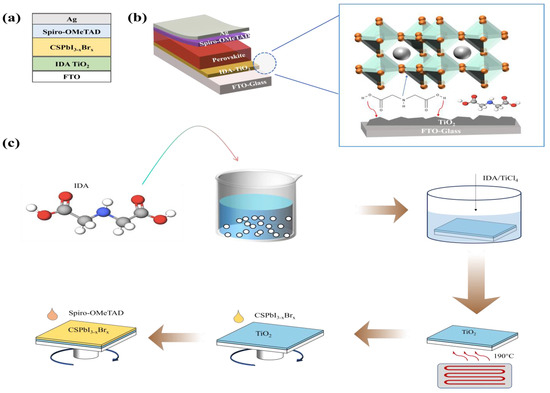
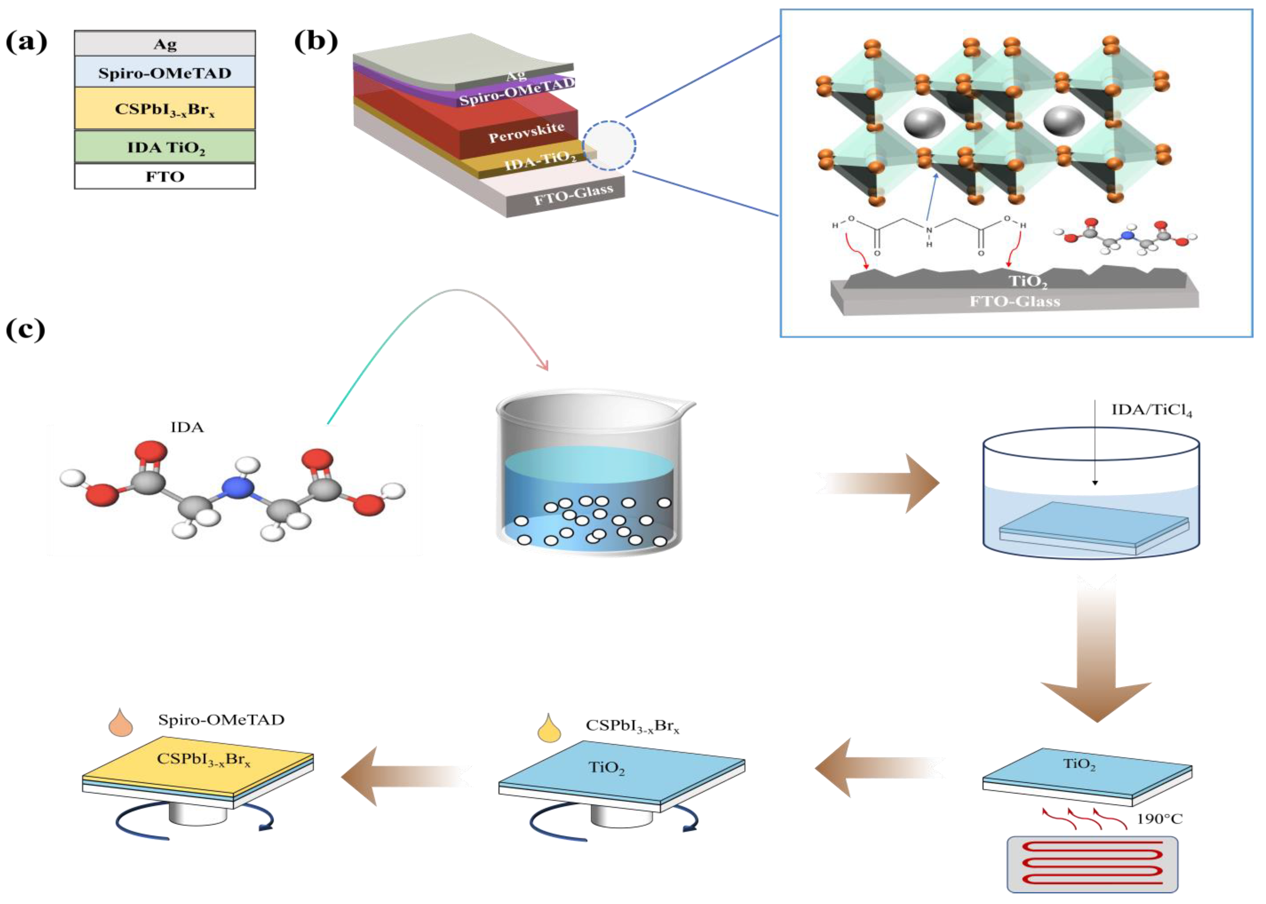
The schematic illustration of device structure, working principle, and large area manufacturing flow chart of the IDA-functionalized TiO2 (IDA–TiO2)-based PSC is shown in Figure 1. The structure of a typical n-i-p type of planar heterojunction device is shown in Figure 1a, which includes FTO glass/IDA−TiO2 ETL/CsPbI3−xBrx perovskite absorber/Spiro−OMeTAD/HTL/Ag top electrode. The IDA−TiO2 ETL was strategically introduced to overcome the inherent limitations of pure TiO2 (high defect density and inferior interfacial compatibility), through efficient electron extraction, hole blocking, and defect passivation [25,26].
Figure 1.
(a) The device structure of the PSCs. (b) Schematic representation of the IDA function between the TiO2 film and the perovskite film. (c) IDA was added dropwise to the aqueous solution of TiCl4 and the annealing process of perovskite and ETL films.
The 3D illustration of the whole device stack as well as the zoom-in image at the IDA−TiO2/CsPbI3−xBrx heterojunction is shown in Figure 1b, which helps us better understand how IDA can act as a capping agent for both suppressing nonradiative recombination centers—by forming strong bidentate ligand complexation between IDA’s carboxylic acid group and surface Ti4+ cations or oxygen vacancies residing within TiO2 lattices [27]—and promoting charge transfer by extending conjugated π-bridge between the perovskite layer and ETL. Simultaneously, the -NH- group coordinates to undercoordinated Pb2+ ions at the perovskite grain boundaries and interface to suppress ion migration and to enhance interface adhesion [28,29]. The schematic flow chart for our step-by-step fabrication process based on the hydrothermal method is shown in Figure 1c, which starts from preparing an appropriate and stable IDA−TiCl4 precursor through dissolving IDA in an ice-water–TiCl4 solution, after which the samples were subjected to a hydrothermal treatment for growing IDA-modified TiO2 nanoparticles in situ. The final IDA−TiO2 dispersion is subsequently cast on FTO glass followed by post-deposition annealing (at 190 °C) for film densification, absorbing IDA to the TiO2 surface, and removing excess solvent. Finally, the full device was completed via subsequent spin-coating of the CsPbI3−xBrx perovskite absorber and Spiro−OMeTAD HTL, after which we perform thermal evaporation of the Ag top electrode. The homogeneous distribution of IDA in the TiO2 matrix via this hydrothermal approach can provide effective passivation to defects as well as efficient interfacial engineering for achieving excellent PSC performance [30].
To clarify the interaction mechanism between IDA and the TiO2 ETL as well as the perovskite layer, we conducted optical photography, X-ray photoelectron spectroscopy (XPS), and Fourier transform infrared spectroscopy (FTIR) analyses.
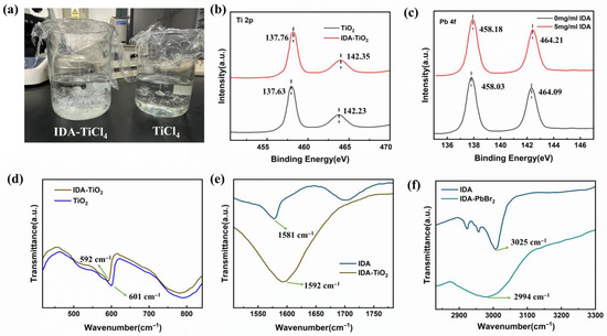
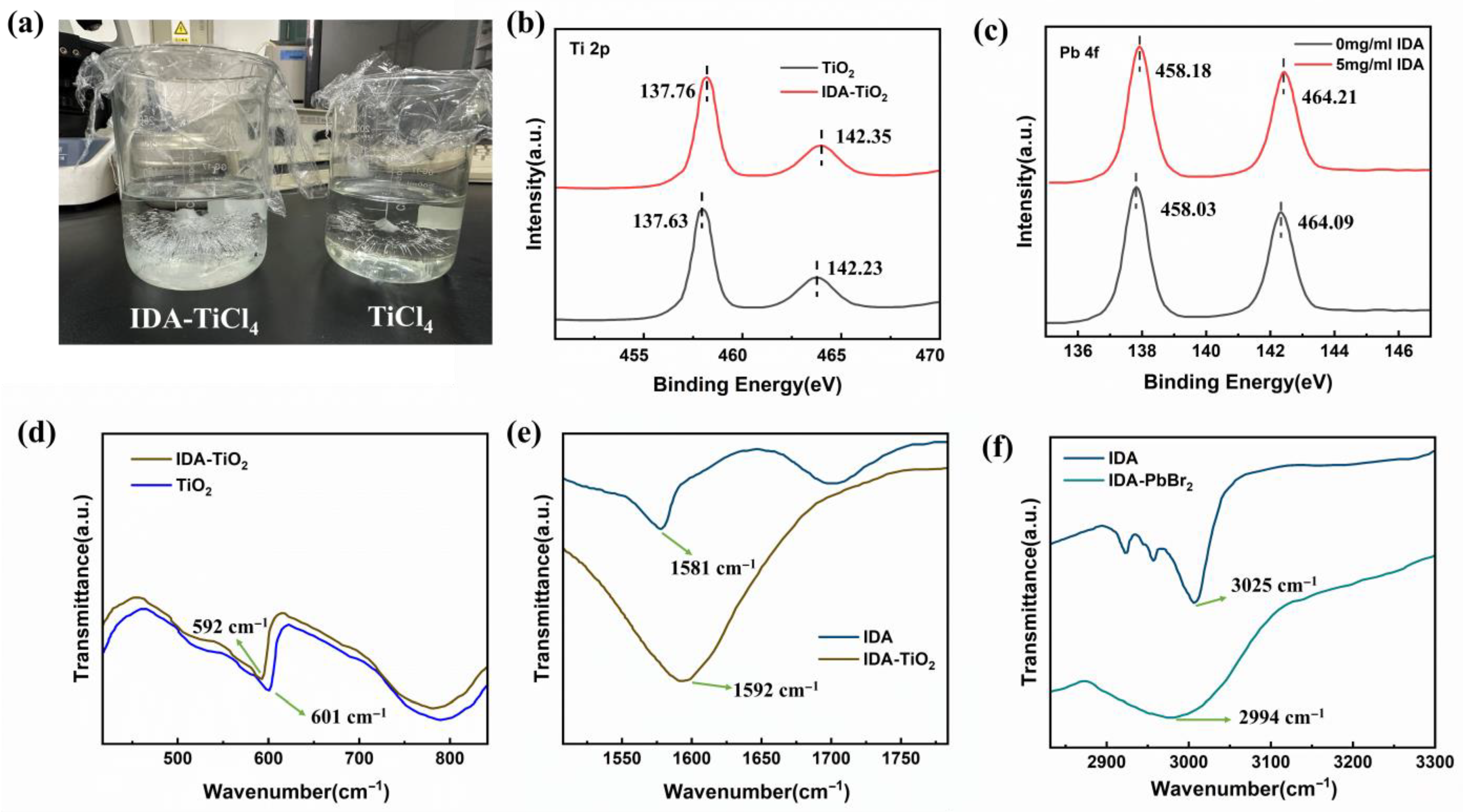
Figure 2a shows the TiCl4 precursor solution with and without IDA after 1 h on ice: the pure solution turned turbid due to rapid Ti4+ hydrolysis forming large TiO2 colloids, whereas the IDA-containing solution remained clear—demonstrating that IDA’s carboxyl groups coordinate Ti4+, suppressing hydrolysis and nanoparticle agglomeration [31].
Figure 2.
(a) Digital photographs show IDA–TiCl4 and pure TiCl4 solutions after 1 h in an ice bath: IDA suppresses rapid TiCl4 hydrolysis. (b) XPS spectra of Ti 2p for pristine TiO2 and IDA–TiO2 films. (c) XPS spectra of Pb 4f for perovskite films deposited on pristine TiO2 and IDA–TiO2 ETLs. (d) FTIR spectra of TiO2 and IDA–TiO2 focusing on the Ti-O stretching vibration region. (e) FTIR spectra of pure IDA and IDA–TiO2 in the C=O stretching vibration region. (f) FTIR spectra of pure IDA and the IDA–PbBr2 complex in the N–H stretching vibration region.
XPS further confirms the chemical interaction: in the IDA-modified TiO2 film, the Ti 2p3/2 and Ti 2p1/2 peaks shift positively to 458.18 eV and 464.21 eV—versus 458.03 eV and 464.09 eV for pure TiO2—indicating reduced electron density around Ti atoms and thus strong coordination between Ti sites and IDA’s carboxyl groups (-COOH). Furthermore, to investigate the interaction between IDA and the perovskite layer, we analyzed the Pb 4f spectra (Figure 2c). The Pb 4f peaks for the perovskite deposited on IDA–TiO2 (137.76 eV and 142.35 eV) show a distinct shift compared to the control sample (137.63 eV and 142.23 eV). This variation in binding energy serves as evidence that the functional groups of IDA (-NH-) interact with the Pb2+ ions at the buried interface, effectively passivating interfacial defects [32].
FTIR spectroscopy provides strong structural evidence for interfacial coordination. As shown in Figure 2d, the Ti–O stretching vibration peak shifts from 601 cm−1 for pure TiO2 to 592 cm−1 for IDA–TiO2, which is consistent with the elongation of the Ti–O bond after IDA anchoring. In Figure 2e, after IDA binds to TiO2, its C=O stretching vibration peak red-shifts from 1581 cm−1 to 1592 cm−1, confirming that carboxyl groups chelate with surface Ti4+ sites in a bidentate form. In Figure 2f, the N–H stretching vibration peak of IDA (3025 cm−1) red-shifts to 2994 cm−1 in the IDA–PbBr2 complex, indicating that the nitrogen atom on -NH- donates lone pair electrons to undercoordinated Pb2+—this is a key interaction for interfacial defect passivation.
These results collectively indicate that IDA can act as a bifunctional molecular bridge: its carboxyl group firmly anchors to the TiO2 surface, while -NH- effectively passivates the defects at the electron transport layer/perovskite interface [33].
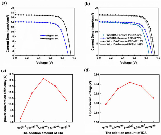
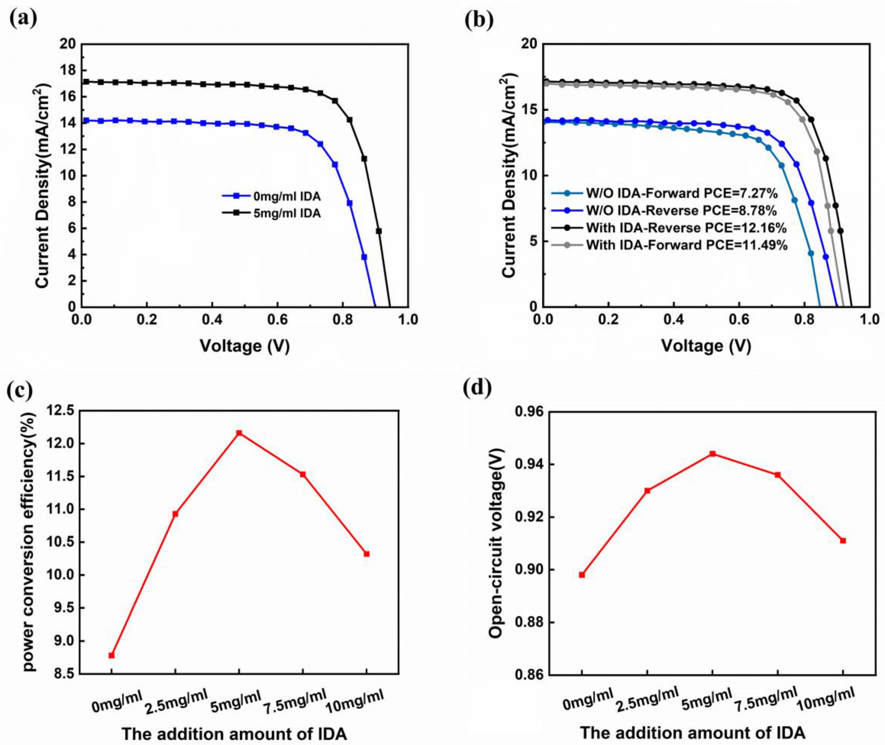
Figure 3a shows the J-V characteristic curves measured under standard AM 1.5G illumination. The results indicate that the device with the IDA-modified TiO2 electron transport layer (5 mg/mL) exhibits significantly improved photovoltaic parameters compared to the pristine TiO2 control device: the Jsc increases from 14.22 mA/cm2 to 17.17 mA/cm2, the Voc rises from 0.898 V to 0.944 V, and the FF improves from 71.04% to 75.15%. Additionally, the JV curve shows better saturation characteristics, with higher current output at forward bias, indicating improved charge extraction and reduced interface recombination [34]. These trends are also systematically quantified in Table 1.
Figure 3.
(a) J-V characteristic curves of PSCs prepared with IDA. (b) The J-V curves of the devices with and without IDA measured in the reverse and forward scanning directions. (c) PCE variations as a function of IDA concentration. (d) The Voc varies with the amount of IDA added.
Table 1.
Performance Parameters of PSCs Prepared with Different Concentrations of IDA.
To further assess the reliability of the device performance and the quality of the interface, we investigated the J-V hysteresis behaviors, as shown in Figure 3b. The hysteresis index (HI) was calculated using the following equation:
PCEReverse and PCEForward denote reverse-scan and forward-scan photovoltaic efficiencies, respectively. Pure-TiO2 devices show large J-V hysteresis (HI = 0.172), whereas IDA-modified devices exhibit nearly hysteresis-free behavior (HI = 0.055). This confirms that IDA passivates interfacial defects and enables balanced charge extraction, suppressing ion-accumulation-induced capacitance [35,36].
As illustrated in Figure 3c,d, the PCE and Voc exhibit a volcano-shaped dependence on IDA concentration. Specifically, the device performance peaks at an optimal concentration of 5 mg/mL, achieving a maximum PCE of 12.16% (a relative enhancement of 38.9%), Voc of 0.944 V, and FF of 75.15%. This improvement stems from the dual role of IDA: at lower concentrations, it effectively passivates TiO2 trap states, whereas at higher concentrations, it optimizes the interface for enhanced electron extraction and reduced recombination [37]. However, excessive IDA (beyond 5 mg/mL) leads to the aggregation of TiO2 nanoparticles, creating new interfacial defects that hinder electron transport and degrade device performance [38]. Consequently, 5 mg/mL is identified as the optimal dosage for maximizing the synergistic enhancement of Jsc, Voc, and FF.
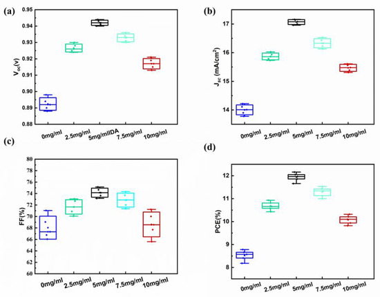
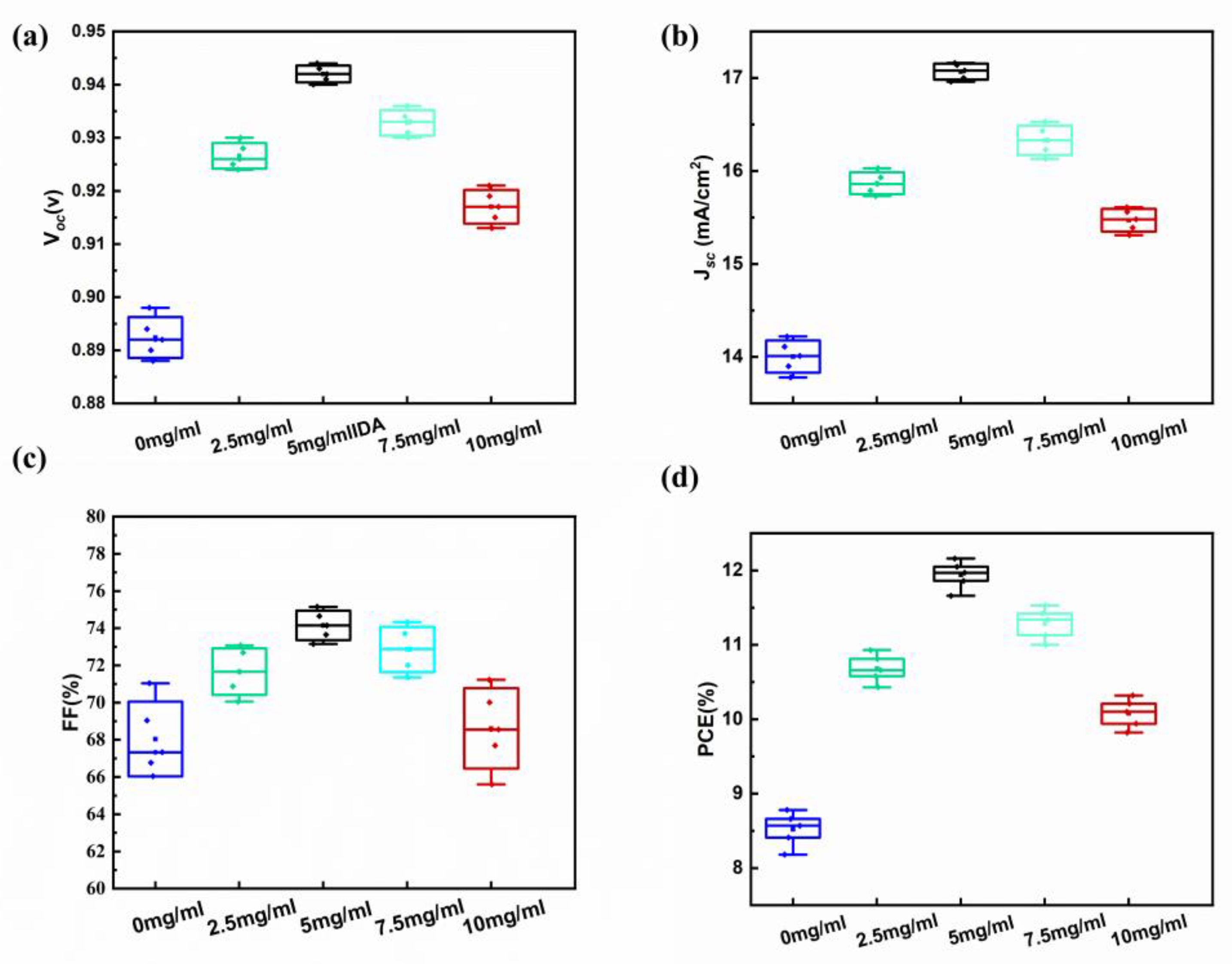
To further confirm the repeatability and consistency of the enhanced PV performances achieved with IDA-modified TiO2 ETLs, a total of 16 devices were fabricated over the range of different IDA doping concentrations (0, 2.5, 5, 7.5, and 10 mg/mL), employing identical solution-processing protocols. A representation of device performances obtained for all the devices is shown in Figure 4, which shows box-and-whisker plots of the Voc, Jsc, FF, and PCE over the various IDA concentrations. It is interesting to note that the cells with 5 mg/mL IDA have the largest medians of all four PV parameters, and the small size of the box for the 5 mg/mL IDA group suggests that there is little difference in their performances between different parallel devices, indicating good reproducibility of the processes. On the other hand, a lower average (median value) as well as larger spread of values is observed for devices using pure TiO2 layers and IDAs in excess of 5 mg/mL, confirming that 5 mg/mL is the optimal doping concentration of IDA modification.
Figure 4.
Performance characteristics of CsPbI3−xBrx PSCs devices as a function of varying amounts of IDA: (a) Voc, (b) Jsc, (c) FF, and (d) PCE.
All these results together indicate that IDA-treated TiO2 ETLs not only improve maximum PCE for CsPbI3−xBrx-based PSCs but are also reliable, with good reproducibility between different batches of devices, highlighting the effectiveness of the introduced interfacial engineering approach.
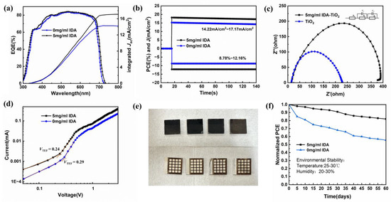
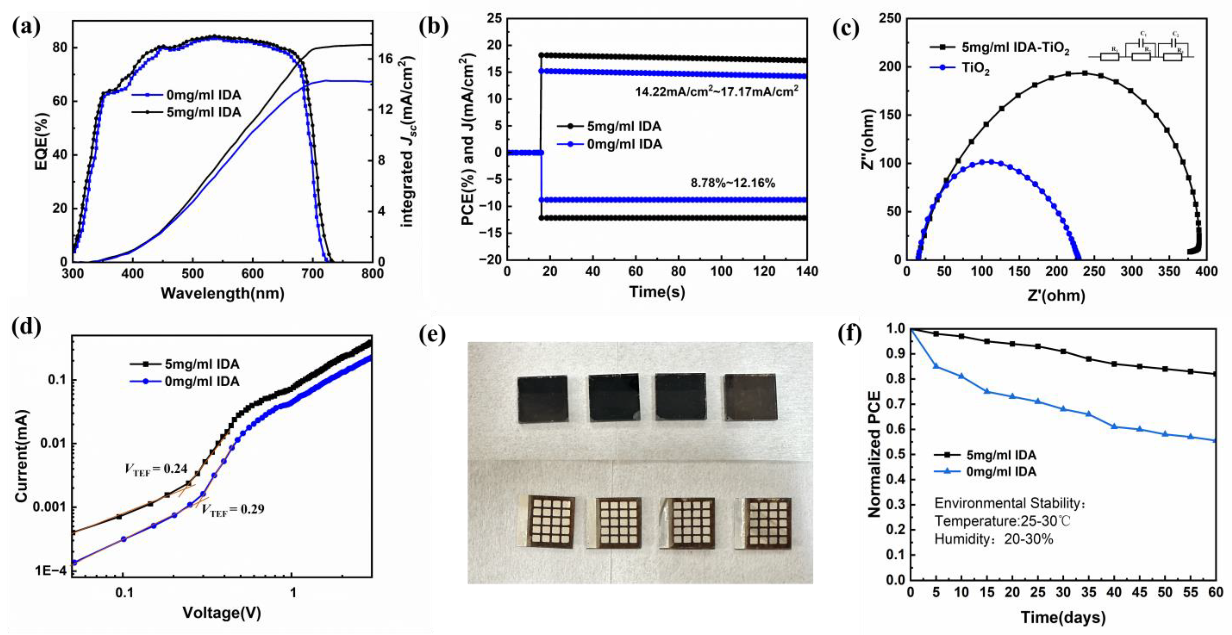
To validate the J-V measurements and probe spectral response, we acquired external quantum efficiency (EQE) spectra (Figure 5a). The IDA-modified TiO2 device shows enhanced and broadened photo response across the visible range, outperforming the control. The current density obtained by EQE spectral integration yielded 17.00 mA/cm2 for the modified device and 14.06 mA/cm2 for the control device, which is highly consistent with the results obtained from J-V scanning.
Figure 5.
(a) EQE spectra of PSCs based on pristine and IDA-modified TiO2 ETLs. (b) Steady-state Jsc and PCE output, tracked over 140 s under continuous AM 1.5G illumination. (c) EIS analysis of devices based on different ETLs. (d) SCLC curves for electron-only devices. (e) Physical photographs of the unencapsulated IDA-modified devices (front and back views) every 15 days. (f) Long-term environmental stability curves of normalized PCE for devices based on pristine and IDA-modified TiO2 ETLs stored in ambient air (25–30 °C, 20–30% RH) for 60 days.
To verify the reliability of the photovoltaic performance, a 140 s test was conducted on the steady-state power output at the maximum power point [39,40]. As shown in Figure 5b, the steady-state current density of the device modified by IDA was 17.17 mA/cm2, with a PCE of 12.16%, and no attenuation was observed. This is in complete agreement with the J-V scan results, demonstrating the stability and reliability of the device efficiency, which contrasts sharply with the lower performance of the control device (8.78%).
To deeply investigate the charge recombination kinetics and defect density, electrochemical impedance spectroscopy (EIS) and space-charge-limited current (SCLC) tests were conducted. Figure 5c shows the Nyquist plot of the device. Compared with the pure TiO2 device, the IDA-modified device presents a significantly larger semicircle in the low-frequency region. The substantial increase in the recombination resistance indicates that the IDA modification can effectively suppress the carrier recombination at the electron transport layer/perovskite interface [41].
To estimate the defect density of perovskite films, space-charge-limited current (SCLC) measurements were conducted on electron-only devices with the structure FTO/IDA–TiO2/CsPbI3−xBrx/PCBM/Ag, as shown in Figure 5d. The trap-filled limit voltage (VTFL) was extracted, and the trap density (Nt) was calculated using the following equation [42]:
In this expression, ε0 is the vacuum permittivity, εr is the relative dielectric constant, is the elementary charge, and L is the thickness (~500 nm) of the perovskite layer [24]. As seen from Figure 5d, the trap-filled limit voltage (VTFL) is 0.29 V for the pristine device, while it decreases to 0.24 V for the device modified with 5 mg/mL IDA. The corresponding trap densities are 3.72 × 1015 cm−3 and 3.08 × 1015 cm−3, respectively. These results confirm that the introduction of IDA effectively passivates interfacial and grain boundary defects. This observation is consistent with the PL quenching behavior, verifying the key role of IDA in defect inhibition and charge transport enhancement.
Finally, the long-term stability of the unencapsulated devices was evaluated under ambient conditions (25–30 °C, 20–30% relative humidity). Figure 5e records the morphological evolution of the IDA-modified device over 60 days, with photographs taken every 15 days from both the front and rear sides. Notably, the device maintains its original deep black color throughout the test, without any bleaching or yellowing (a typical signature of the phase transition to the non-photoactive δ-phase). This direct visual evidence strongly demonstrates that IDA modification significantly improves the resistance of perovskite films against moisture-induced degradation.
To quantitatively evaluate the stability, the PCE of the devices was recorded every 5 days, as shown in Figure 5f). The IDA-modified device exhibits excellent stability, retaining over 82% of its initial efficiency after 60 days. In contrast, the control device degrades rapidly, maintaining only about 55% of its original performance. The improved stability is attributed to the modification effect of IDA.
3.2. Characterization of IDA–TiO2 ETL
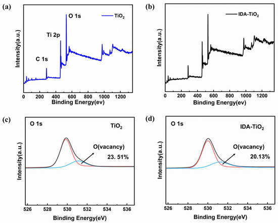
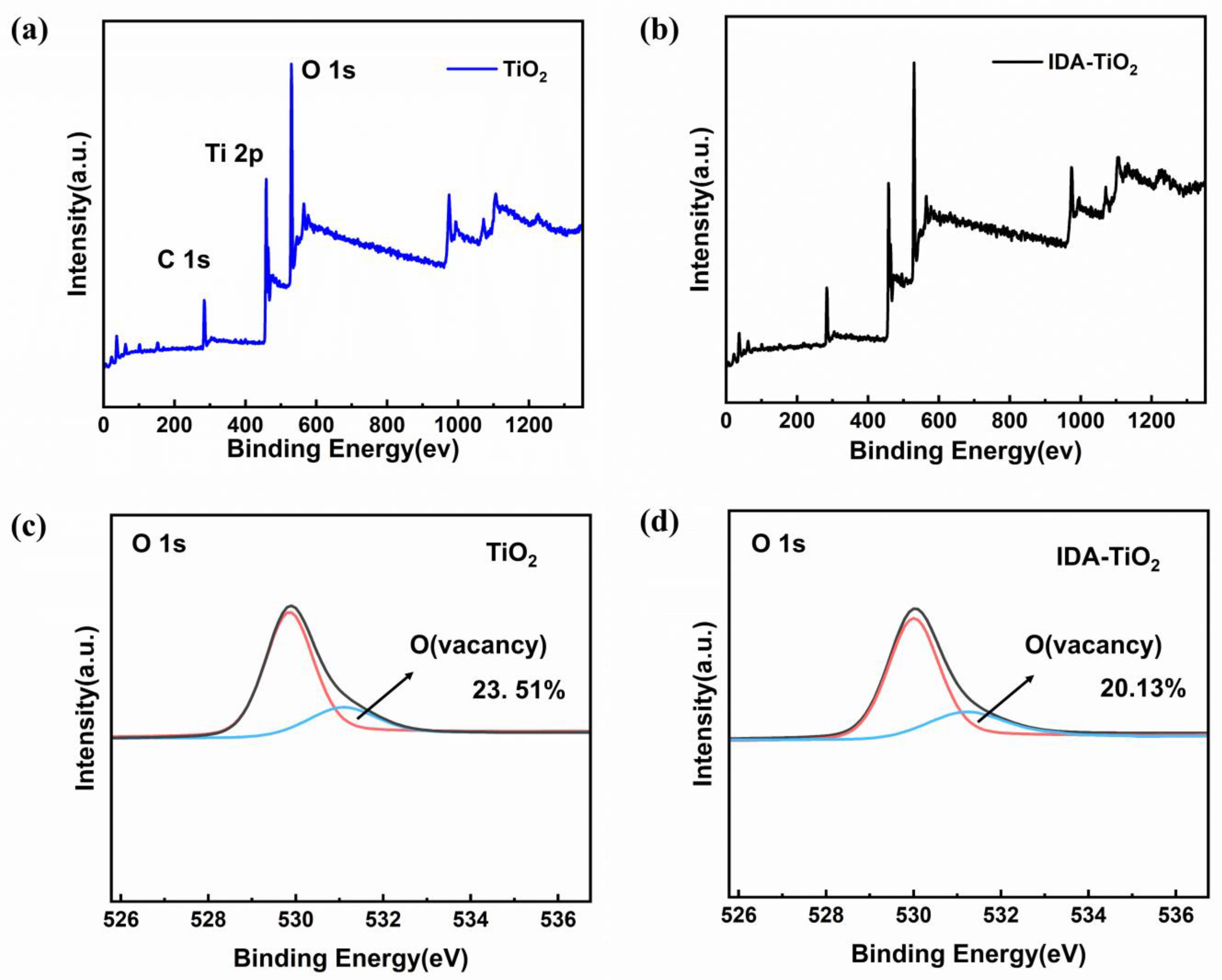
To systematically investigate the influence of IDA on the surface chemical states and defect density of the electron transport layer, XPS measurements were performed. Full-spectrum XPS scans of the pristine TiO2 and IDA-modified TiO2 films are presented in Figure 6a,b, respectively. Subsequent deconvolution of the O 1s core-level spectra—shown in Figure 6c,d—reveals two distinct components: a dominant peak centered at ~529.9 eV, assigned to lattice oxygen in Ti–O bonds (denoted as OL), and a higher-binding-energy shoulder at ~531.5 eV, attributed to oxygen vacancies and/or surface-adsorbed hydroxyl species (denoted as Ov). Oxygen vacancies constitute prototypical electron trap states that impede charge transport and promote nonradiative recombination [43].
Figure 6.
(a) XPS survey spectra of the pristine TiO2. (b) XPS survey spectra of the pristine IDA–TiO2. (c) O 1s XPS spectra of the pristine TiO2. (d) O 1s XPS spectra of the IDA–TiO2.
Quantitative analysis indicates that the relative contribution of the Ov component decreases from 23.51% in pristine TiO2 to 20.13% in the IDA-modified film. This reduction strongly suggests that the carboxyl groups (-COOH) of IDA molecules effectively coordinate with under-coordinated surface Ti atoms, thereby passivating oxygen vacancy defects [44]. Such passivation suppresses detrimental trap states, leading to an enhanced structural order at the TiO2 surface. Consequently, electron extraction efficiency is expected to improve, while interfacial nonradiative recombination losses are minimized. This finding provides a direct chemical rationale for the experimentally observed reduction in Nt reported in the preceding electrical characterization.
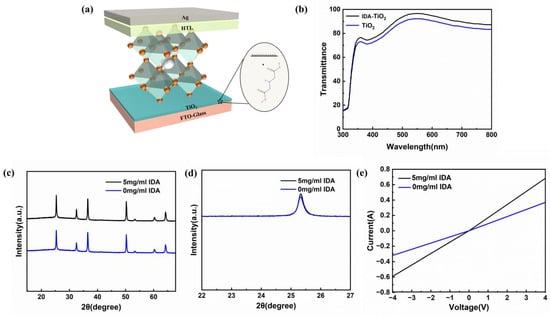
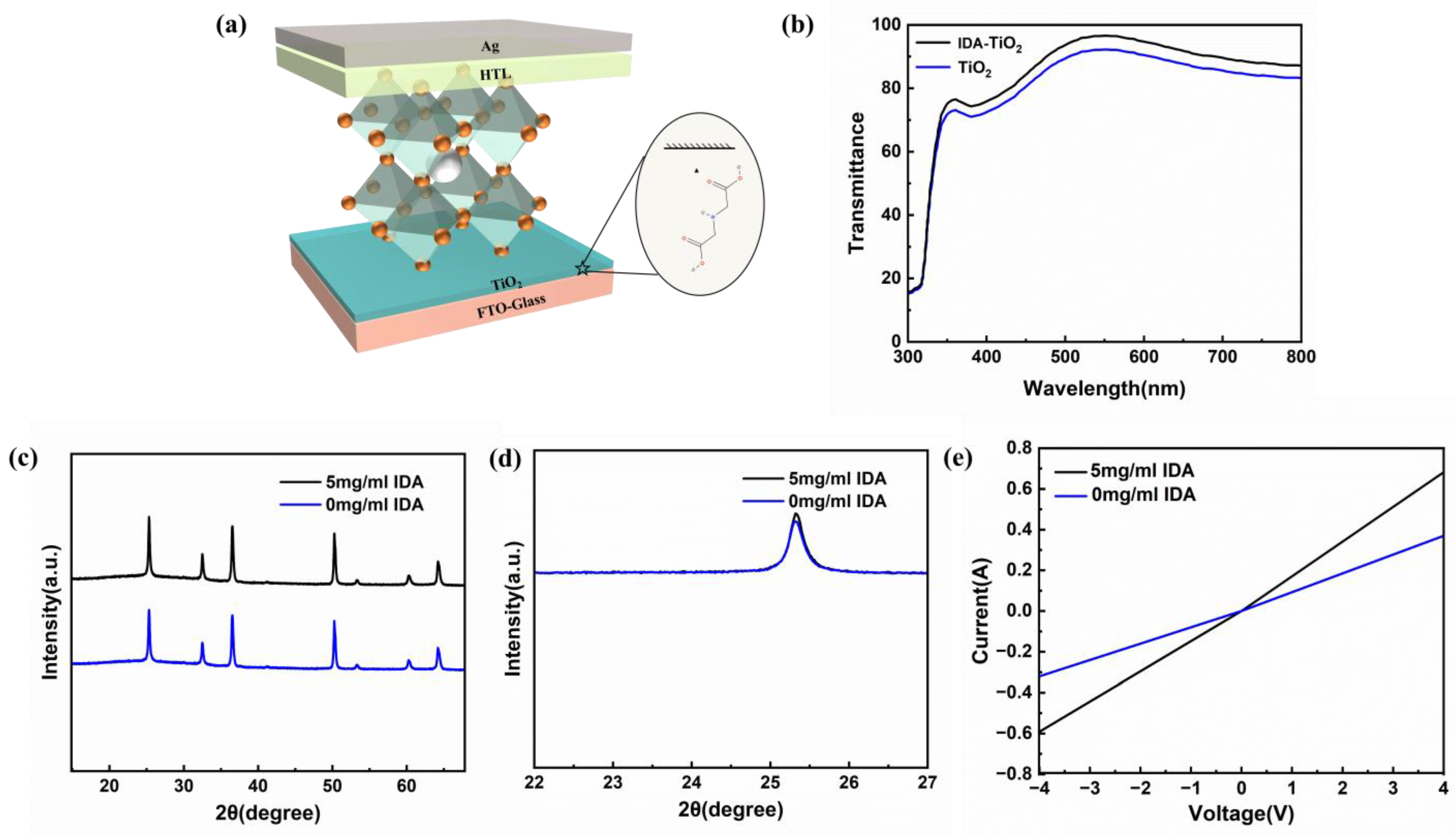
We investigated the effects of IDA on the physical and electrical properties of TiO2 films. The schematic diagram of the device structure is shown in Figure 7a, where the IDA molecules act as interface-connecting molecules between the ETL and the perovskite layer.
Figure 7.
(a) The schematic diagram representing an interfacial process occurring in IDA, TiO2, and the CsPbI3−xBrx perovskite film where IDA acts as a molecular linker for defect passivation on the TiO2 surface/perovskite interface. (b) Optical transmittance spectra of the pristine and IDA-modified TiO2 films deposited on FTO glass. (c) X-ray diffraction patterns of IDA–TiO2 and TiO2. (d) Enlarged view of XRD. (e) I–V characteristics of the Ag/ETL/FTO device structure.
Figure 7b presents a comparative analysis of the transmission spectra for the pristine TiO2 film and the IDA-modified TiO2 film. The modified film exhibits slightly enhanced transmittance across the entire visible spectrum (350–800 nm). This improvement suggests that IDA functionalization refines the surface morphology of the TiO2 layer, suppresses light scattering, and thereby facilitates greater photon utilization for photocurrent generation—consistent with the observed increase in Jsc reported in Figure 3.
The crystalline structure of the ETL was characterized by X-ray diffraction (XRD), and the results are displayed in Figure 7c. Both samples show characteristic diffraction peaks assigned to the anatase phase of TiO2. After magnifying the dominant (101) diffraction peak located at approximately 25.3° (Figure 7d), the IDA-modified TiO2 film presents significantly sharper and stronger diffraction signals compared with the pristine sample. This improvement demonstrates that the incorporation of IDA contributes to enhanced crystallinity during thermal annealing and effectively passivates structural defects within the TiO2 layer [45].
To investigate the effect of IDA modification on the conductivity of the TiO2 electron transport layer, we performed I–V measurements using an Ag/ETL/FTO structure (as shown in Figure 7e). It can be seen that IDA–TiO2 film has a steeper slope with larger current density at the same applied voltage than pure TiO2, suggesting that the electrons have better conductivity and mobility. This is attributed to both the passivation of trap states (reduced carrier scattering) and better connectivity between TiO2 nanoparticles (due to IDA’s dispersing action), which facilitates better electron extraction and transport—key reasons for the larger FF and smaller hysteresis of device J–V curves.
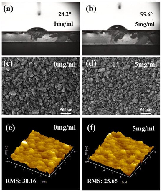
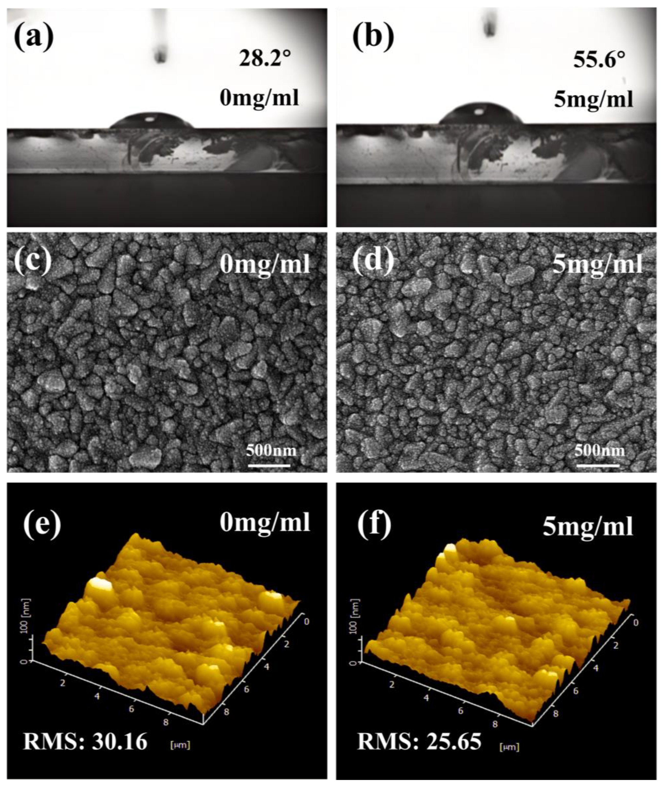
To further investigate the interfacial optimization effects of IDA modification on TiO2 ETLs, we characterized the surface wettability, microscopic morphology, and topographical roughness of pristine and 5 mg/mL IDA-modified TiO2 films, as shown in Figure 8.
Figure 8.
(a,b): Water contact angle measurement of IDA-modified TiO2 films. (c,d): Top-view SEM images of TiO2 films before and after IDA treatment. (e,f) AFM plots of TiO2 films treated with 5mg/mL concentrations of IDA.
The water contact angle (WCA) results are shown in Figure 8a,b. It can be seen that after IDA modification, the WCA rises from 28.2° to 55.6°, thereby changing the surface property from very hydrophilic to relatively hydrophobic, which can tailor the wettability and improve the spreading homogeneity of the CsPbI3−xBrx perovskite precursor solution, which is essential to deposit a continuous and pinhole-free perovskite absorber layer. Figure 8c,d shows SEM photographs of the film before and after calcination. It can be seen that there were many tiny pores on the surface of the pure TiO2 film with irregular particle distribution, whereas for the case of IDA-modified TiO2 films, we observe that particles are packed together in a dense and homogeneous manner, and pores have been greatly diminished. As a result, no direct contact is achieved between the perovskite film and the underlying FTO electrode, minimizing current leakage and interfacial recombination. Figure 8e,f shows AFM topography images, which indicate that IDA treatment decreases the RMS surface roughness of TiO2 from 30.16 nm to 25.65 nm. A smooth surface can not only improve the interfacial adhesion between the ETL and perovskite layer but also promote the growth of bigger, more uniform perovskite grains to reduce even further the number of defects at the ETL/perovskite interface.
Taken together, the above surface characterizations indicate that IDA modification optimizes TiO2 ETL wettability, morphology, and roughness—the key issues enabling the formation of high-quality perovskite films, which in turn are directly responsible for the improved photovoltaic performance and stability of CsPbI3−xBrx PSCs, in line with our previous device performance and mechanistic analysis.
3.3. Impact of IDA–TiO2-Based ETL on Perovskite
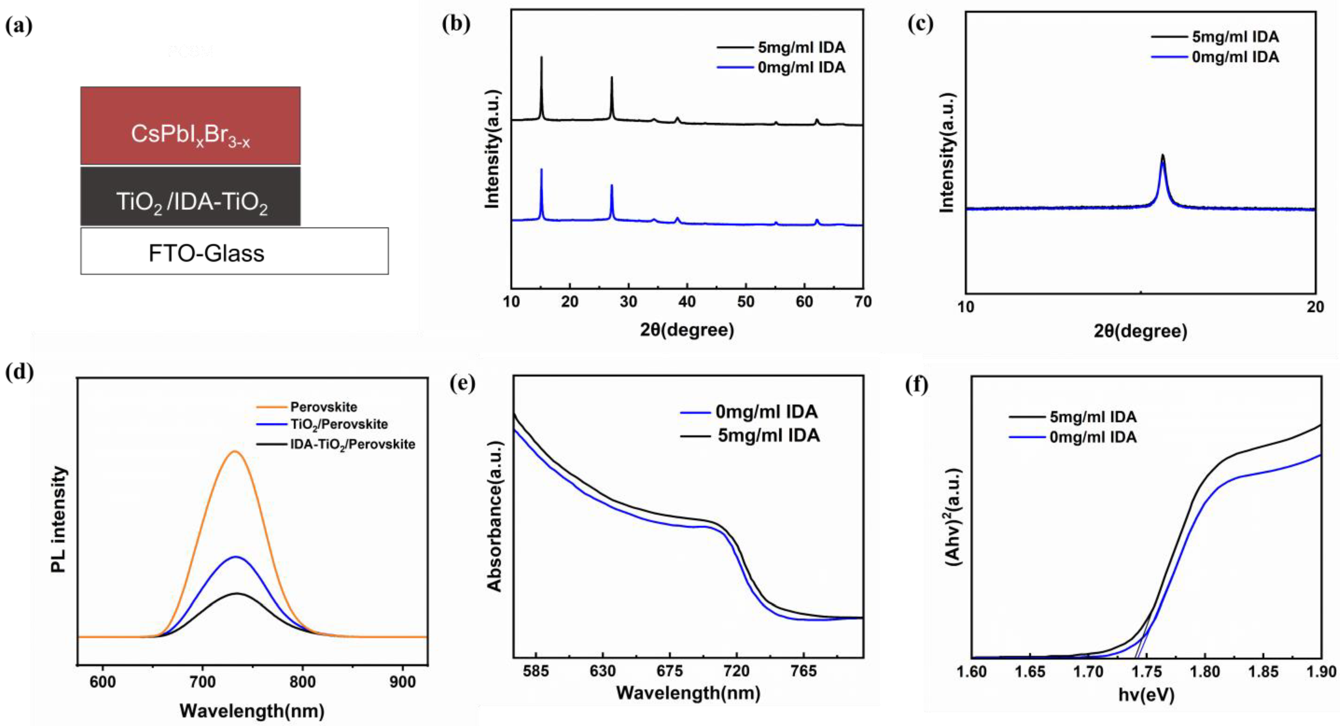
To investigate the influence of the IDA-modified electron transport layer (ETL) on the growth and quality of the upper perovskite layer, we characterized the film structure and optical properties. The structure of the devices is shown in Figure 9a.
Figure 9.
(a) Device structure. (b) XRD patterns of CsPbI3−xBrx perovskite films deposited on pristine TiO2 and 5mg/mL IDA–TiO2 ETLs. (c) Enlarged (100) diffraction peak. (d) PL spectra of CsPbI3−xBrx perovskite layers treated with IDA. (e) UV–Visible absorption spectra of perovskite films. (f) Tauc plots determining the optical bandgap of ~1.74 eV.
Figure 9b presents the XRD patterns of the perovskite films. Both samples exhibit prominent diffraction peaks at 14.4° and 28.9°, corresponding to the (100) and (200) reflections of the cubic (α) phase, confirming the formation of phase-pure perovskite crystals. Figure 9c enlarges the diffraction peak of the (100) crystal plane. It is evident that the diffraction peaks of the films deposited on the IDA-modified TiO2 substrate are sharper and more intense compared to the control group. This increase in peak intensity indicates that the IDA-modified interface can promote the vertical grain growth of the perovskite film and improve the crystallinity. This may be attributed to the reduction in the substrate surface roughness and the improvement of wettability.
The charge extraction capability at the interfaces was evaluated via steady-state photoluminescence (PL) spectroscopy, as shown in Figure 9d. The pristine perovskite film deposited on glass exhibited a strong emission peak centered at approximately 725 nm. Upon integration of the ETL, the PL intensity was significantly quenched—attributable to efficient electron extraction from the perovskite layer. Notably, among all samples, the device incorporating IDA-modified TiO2 exhibited the most pronounced PL quenching relative to the unmodified TiO2 control. This substantial suppression of radiative recombination strongly indicates that IDA passivation effectively mitigates interfacial trap states and enhances electron transfer efficiency from the perovskite absorber to the ETL.
To further investigate the effect of IDA modification on the photoelectric properties of CsPbI3−xBrx films, we performed UV–Vis measurements on perovskite films deposited on bare TiO2 and IDA-modified TiO2 surfaces. As shown in Figure 9e, the absorption spectra of these films are slightly improved after IDA modification, which is attributed to the enhanced crystallinity and the increased grain size of the perovskite confirmed by scanning electron microscopy images. The optical band gap (Eg) was determined from Tauc plots (Figure 9f). Both films exhibited nearly identical band gaps of 1.74 eV, indicating that surface modification enhanced the structural and morphological quality of the perovskite films without perturbing the intrinsic optoelectronic properties of the perovskite material.
Collectively, these results demonstrate that IDA modification of TiO2 ETLs is not only beneficial to the ETL itself but also facilitates the growth of high-quality perovskite films with excellent crystallinity. Meanwhile, this modification enhances light absorption and charge extraction, and these synergistic effects contribute to the improved performance of CsPbI3−xBrx perovskite solar cells.
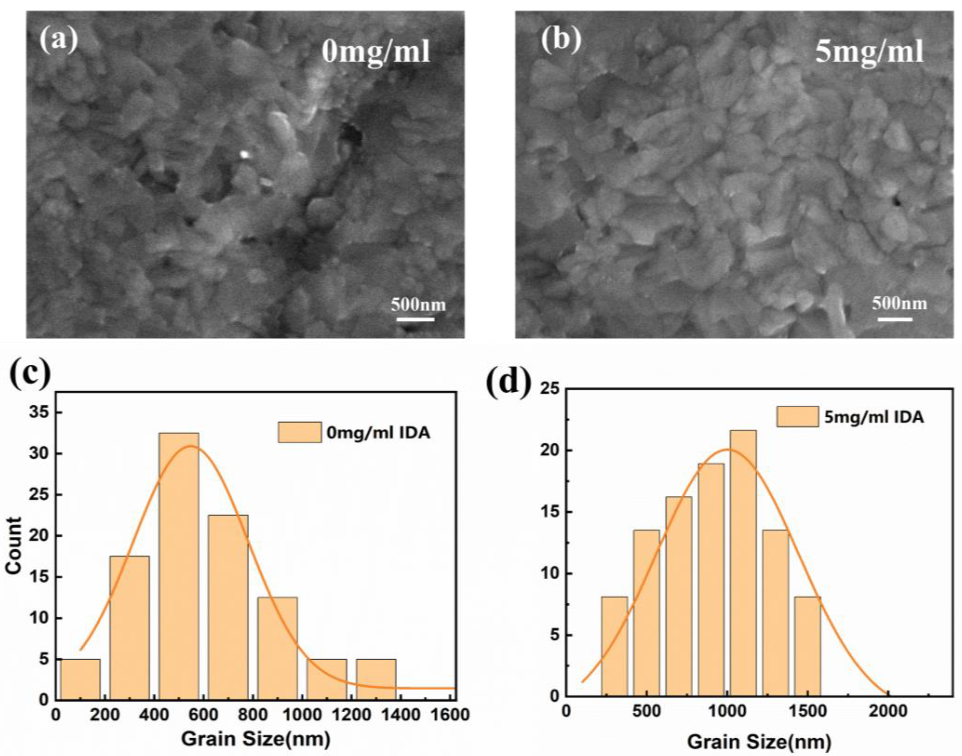
To systematically investigate the effects of the IDA-modified TiO2 ETLs on the growth kinetics and morphology development of the subsequently deposited CsPbI3−xBrx perovskite films, we characterized the surface morphology and grain size distributions of perovskite films grown over pristine and 5 mg/mL IDA-modified TiO2 ETLs, as shown in Figure 10a, which shows the SEM image of the perovskite film grown over pristine TiO2 that exhibits an irregular grain size, smaller grain sizes, as well as the presence of visible pinhole defects on the grain boundaries, which are responsible for acting as a nonradiative center of recombination and reducing the efficiency in charge transport. On the other hand, Figure 10b presents the perovskite film grown on IDA-modified TiO2, exhibiting much flatter and denser morphology with larger, connected grains and fewer pinholes, which is attributed to the improved surface wettability as well as the decreased roughness of the IDA–TiO2 ETL, which favors homogeneous nucleation and the growth of perovskite grain, in agreement with what we observed previously from our contact angle as well as AFM characterization of the ETL surface.
Figure 10.
(a,b): Top-view SEM images of perovskite films before and after IDA treatment. (c,d): The grain statistics of perovskite films before and after IDA treatment.
Figure 10c,d displays the grain size distribution histograms derived from quantitative analysis of SEM micrographs. Statistical analysis of 100 randomly selected grains reveals that the perovskite film deposited on pristine TiO2 exhibits a relatively narrow grain size distribution, with a mean grain size of approximately 550 nm. In contrast, the film grown on IDA–TiO2 displays a broader distribution skewed toward larger grain sizes, with a mean grain size of approximately 950 nm. The observed increase in both average grain size and size uniformity reduces the density of grain boundaries—the primary sites for nonradiative carrier recombination—thereby facilitating more efficient charge transport and mitigating voltage losses. This morphological enhancement is fully consistent with our prior photovoltaic performance measurements, corroborating that IDA functionalization of the TiO2 ETL not only improves the intrinsic properties of the ETL but also promotes the formation of high-quality, large-grained perovskite films, ultimately leading to substantial improvements in device photovoltaic efficiency.
4. Conclusions
This study demonstrates that IDA is an efficient multifunctional modifier for TiO2 ETLs in inorganic CsPbI3−xBrx PSCs. IDA modification synergistically optimizes TiO2 ETL optoelectronic properties, ETL/perovskite interfacial compatibility, and perovskite film quality, thereby enhancing both device efficiency and stability.
Systematic characterization reveals that IDA passivates TiO2 defects to enhance electron transport/extraction, improves visible-light transmittance to efficiently harvest photons, and facilitates the formation of dense TiO2 films as well as large-grained perovskite film with lower recombination. This optimal cell (5 mg/mL IDA) exhibits a PCE value of 12.16%, representing a relative enhancement of 38.9% compared to the control device (8.78%), along with less hysteresis effect. Stability tests without encapsulation at room temperature (25–30 °C, 20–30% RH) demonstrate that the IDA-modified devices retain 82% of their original PCE after 60 days, as compared with only 60% retention of the pristine TiO2 control, suggesting substantial improvements in operation stability.
Importantly, this IDA modification strategy is a facile one-step additive strategy to the TiCl4 precursor, which can be scaled up by solution process without complicated post-treatments; its double roles (carboxy-TiO2 anchoring and imino-perovskite interaction) are responsible for both efficiency and stability enhancements. In this study, we demonstrate a low-cost and practicable way of interfacial engineering toward higher performance, stable inorganic PSCs.
Author Contributions
Conceptualization, F.Z. and G.L.; methodology, G.L.; validation, C.C. and K.G.; formal analysis, F.Z.; resources, F.Z.; data curation, G.L.; writing—original draft preparation, G.L.; writing—review and editing, F.Z.; visualization, G.L.; supervision, X.W.; project administration, X.W.; funding acquisition, F.Z. All authors have read and agreed to the published version of the manuscript.
Funding
This research was funded by the National Natural Science Foundation of China (grant number 62305202), the Technology Innovation Leading Program of Shaanxi (grant number 2025ZC-YYDP-32, 2023GXLH-076), and the 2023 “Three Reforms” Achievement Transformation Project of Xianyang (grant number L2023-ZDKJ-QCY-SXGG-GY-099).
Data Availability Statement
The original contributions presented in this study are included in the article. Further inquiries can be directed to the corresponding author.
Acknowledgments
The authors would like to thank the Analysis and Testing Center of Shaanxi University of Science and Technology for their assistance with the characterization measurements.
Conflicts of Interest
The authors declare no conflicts of interest.
References
- Kojima, A.; Teshima, K.; Shirai, Y.; Miyasaka, T. Organometal halide perovskites as visible-light sensitizers for photovoltaic cells. J. Am. Chem. Soc. 2009, 131, 6050–6051. [Google Scholar] [CrossRef] [Scilit] [PubMed]
- Green, M.A.; Dunlop, E.D.; Hohl-Ebinger, J.; Yoshita, M.; Kopidakis, N.; Bothe, K.; Hinken, D.; Rauer, M.; Hao, X. Solar cell efficiency tables. Prog. Photovolt. Res. Appl. 2024, 32, 3–13. [Google Scholar] [CrossRef] [Scilit]
- Yoo, J.J.; Seo, G.; Chua, M.R.; Park, T.G.; Lu, Y.; Rotermund, F.; Kim, Y.-K.; Moon, C.S.; Jeon, N.J.; Correa-Baena, J.-P.; et al. Efficient perovskite solar cells via improved carrier management. Nature 2021, 590, 587–593. [Google Scholar] [CrossRef] [Scilit] [PubMed]
- Liao, Y.-H.; Chang, Y.-H.; Lin, T.-H.; Lee, K.-M.; Wu, M.-C. Recent Advances in Metal Oxide Electron Transport Layers for Enhancing the Performance of Perovskite Solar Cells. Materials 2024, 17, 2722. [Google Scholar] [CrossRef] [Scilit]
- O’Regan, B.; Grätzel, M. A low-cost, high-efficiency solar cell based on dye-sensitized colloidal TiO2 films. Nature 1991, 353, 737–740. [Google Scholar] [CrossRef] [Scilit]
- Anaraki, E.H.; Kermanpur, A.; Steier, L.; Domanski, K.; Matsui, T.; Tress, W.; Saliba, M.; Abate, A.; Grätzel, M.; Hagfeldt, A. Highly efficient and stable planar perovskite solar cells by low-temperature solution-processed tin oxide. Energy Environ. Sci. 2016, 9, 3128–3134. [Google Scholar] [CrossRef] [Scilit]
- Chen, Q.; Yuan, L.; Duan, R.; Huang, P.; Fu, J.; Ma, H.; Wang, X.; Zhou, Y.; Song, B. Zwitterionic Polymer: A Facile Interfacial Material Works at Both Anode and Cathode in p-i-n Perovskite Solar Cells. Sol. RRL 2019, 3, 1900118. [Google Scholar] [CrossRef] [Scilit]
- Tiwana, P.; Docampo, P.; Johnston, M.B.; Snaith, H.J.; Herz, L.M. Electron mobility and injection efficiency in mesoporous nanocrystalline TiO2 films. ACS Nano 2011, 5, 5158–5166. [Google Scholar] [CrossRef] [Scilit]
- Li, W.; Fan, J.; Li, J.; Mai, Y.; Wang, L. Controllable grain growth of perovskite crystals by organic-additive-containing precursors. J. Am. Chem. Soc. 2015, 137, 10399–10405. [Google Scholar] [CrossRef] [Scilit]
- Shao, Y.; Xiao, Z.; Bi, C.; Yuan, Y.; Huang, J. Origin and elimination of photocurrent hysteresis by surface passivation in CH3NH3PbI3 perovskite solar cells. Nat. Commun. 2014, 5, 5784. [Google Scholar] [CrossRef] [Scilit]
- Chen, B.; Yang, M.; Zheng, X.; Wu, C.; Li, S.; Huang, J. Impact of capacitive effect and ion migration on the hysteretic behavior of perovskite solar cells. J. Phys. Chem. Lett. 2015, 6, 4693–4700. [Google Scholar] [CrossRef] [Scilit] [PubMed]
- Mahmoudi, T.; Wang, Y.; Hahn, Y.B. Graphene and its derivatives for high performance perovskite solar cells. Nano Energy 2018, 47, 51–65. [Google Scholar] [CrossRef] [Scilit]
- Le Corre, V.M.; Duijnstee, E.A.; El Tambouli, O.; Ball, J.M.; Snaith, H.J.; Lim, J.; Koster, L.J.A. Revealing charge carrier mobility and defect densities in metal halide perovskites via space-charge-limited current measurements. ACS Energy Lett. 2021, 6, 1087–1094. [Google Scholar] [CrossRef] [Scilit] [PubMed]
- Giordano, F.; Abate, A.; Correa Baena, J.P.; Saliba, M.; Matsui, T.; Im, S.H.; Zakeeruddin, S.M.; Nazeeruddin, M.K.; Hagfeldt, A.; Graetzel, M. Enhanced electronic properties in mesoporous TiO2 via lithium doping for high-efficiency perovskite solar cells. Nat. Commun. 2016, 7, 10379. [Google Scholar] [CrossRef] [Scilit]
- Cao, J.; Jin, B.; Li, S.; Zheng, J.; Keremane, K.; Priya, S.; Hu, X.; Wu, C.; Wang, K. Structural Properties of Perovskite. In Perovskite Optoelectronic Devices; Springer: Cham, Switzerland, 2024; pp. 19–50. [Google Scholar] [CrossRef] [Scilit]
- Keremane, K.S.; Prathapani, S.; Haur, L.J.; Bruno, A.; Priyadarshi, A.; Adhikari, A.V.; Mhaisalkar, S.G. Improving the Performance of Carbon-Based Perovskite Solar Modules (70 cm2) by Incorporating Cesium Halide in Mesoporous TiO2. ACS Appl. Energy Mater. 2021, 4, 249–258. [Google Scholar] [CrossRef] [Scilit]
- Wu, Z.; Wu, J.; Wang, S.; Wang, G.; Shen, L.; Xu, G.; Zhang, C.; Zhang, H.; Lu, Y.; Zeng, H. Multifunctional molecule of cystamine dihydrochloride for high-efficient perovskite solar cells. Chem. Eng. J. 2022, 449, 137851. [Google Scholar] [CrossRef] [Scilit]
- Tan, H.; Jain, A.; Voznyy, O.; Lan, X.; Garcia de Arquer, F.P.; Fan, J.Z.; Quintero-Bermudez, R.; Zhugayevych, A.; Hoyt, O.S.; Sargent, E.H. Efficient and stable solution-processed planar perovskite solar cells via contact passivation. Science 2017, 355, 722–726. [Google Scholar] [CrossRef] [Scilit]
- Liu, Z.; Li, M.; Cai, X.; Wang, X.; Jiang, J.; Li, Y.; Song, Y.; Wang, X.-F. Perovskite Solar Cells Based on Polymerized Chlorophyll Films as Environmentally Friendly Hole-Transporting Layers. Small 2024, 20, 2305484. [Google Scholar] [CrossRef] [Scilit]
- Wang, Y.; Tian, Y.; Yang, Z.; Wang, L.; Wang, S. High-efficiency and stable all-inorganic CsPbI3 perovskite solar cells enabled by interfacial engineering. Science 2019, 365, 591–595. [Google Scholar] [CrossRef] [Scilit]
- Eperon, G.E.; Paternò, G.M.; Sutton, R.J.; Zampetti, A.; Haghighirad, A.A.; Cacialli, F.; Snaith, H.J. Inorganic caesium lead iodide perovskite solar cells: Overcoming thermodynamic instability via regional nucleation. J. Mater. Chem. 2015, 3, 19688–19695. [Google Scholar] [CrossRef] [Scilit]
- Li, Z.; Klein, T.R.; Kim, D.H.; Yang, M.; Berry, J.J.; van Hest, M.F.A.M.; Zhu, K. Scalable fabrication of perovskite solar cells. Nat. Rev. Mater. 2018, 3, 18017. [Google Scholar] [CrossRef] [Scilit]
- Hancock, R.D.; Martell, A.E. Ligand design for selective complexation of metal ions in aqueous solution. Chem. Rev. 1989, 89, 1875–1914. [Google Scholar] [CrossRef] [Scilit]
- Xue, T.; Li, S.; Chen, Y.; Wang, X.; Zhang, P.; Guo, K.; Zhang, F. Electron beam evaporated SiO2 interfacial layer for improved CsPbI3−xBrx perovskite solar cells. Sol. Energy Mater. Sol. Cells 2025, 292, 113772. [Google Scholar] [CrossRef] [Scilit]
- Xiang, W.; Tress, W. Review on recent progress of all-inorganic metal halide perovskites and solar cells. Adv. Mater. 2019, 31, 1902851. [Google Scholar] [CrossRef] [Scilit] [PubMed]
- Burschka, J.; Pellet, N.; Moon, S.J.; Humphry-Baker, R.; Gao, P.; Nazeeruddin, M.K.; Grätzel, M. Sequential deposition as a route to high-performance perovskite-sensitized solar cells. Nature 2013, 499, 316–319. [Google Scholar] [CrossRef] [Scilit]
- Noel, N.K.; Stranks, S.D.; Abate, A.; Wehrenfennig, C.; Guarnera, S.; Haghighirad, A.A.; Sadhanala, A.; Eperon, G.E.; Johnston, M.B.; Herz, L.M.; et al. Lead-free organic–inorganic tin halide perovskites for photovoltaic applications. Energy Environ. Sci. 2014, 7, 3061–3068. [Google Scholar] [CrossRef] [Scilit]
- Correa-Baena, J.P.; Saliba, M.; Tress, W.; Tvingstedt, K.; Abate, A.; Nazeeruddin, M.K.; Grätzel, M.; Hagfeldt, A. Promises and challenges of perovskite solar cells. Science 2017, 358, 739–744. [Google Scholar] [CrossRef] [Scilit]
- Nunzi, F.; Mosconi, E.; Storchi, L.; Ronca, E.; Selloni, A.; Grätzel, M.; De Angelis, F. Anchoring of Organic Dyes to TiO2: A Computational Study. Energy Environ. Sci. 2013, 6, 1221–1229. [Google Scholar] [CrossRef] [Scilit]
- Wu, W.Q.; Huang, F.; Chen, D.; Cheng, Y.B.; Caruso, R.A. Solvent-mediated dimensional tuning of highly crystalline TiO2 nanorod arrays for n-i-p perovskite solar cells. Adv. Funct. Mater. 2016, 6, 1502027. [Google Scholar] [CrossRef] [Scilit]
- Zhang, X.; Yang, J.; Xu, J.; Zhou, S.; Zhang, Y.; Liu, X.; Zhang, Y.; Li, Y.; Guo, J. Photocatalytic performance of Se-modified TiO2 prepared with triethanolamine or iminodiacetic acid as hydrolysis inhibitors. Mater. Lett. X 2025, 26, 100253. [Google Scholar] [CrossRef] [Scilit]
- Yang, W.; Pan, T.; Yang, G.; Zhu, J.; Ran, X.; Ren, B.; Zuo, M.; Chao, L.; Xia, Y.; Chen, Y. Tailoring interface-anchoring molecules for efficient and stable perovskite solar cells. Nat. Commun. 2025, 16, 11408. [Google Scholar] [CrossRef] [Scilit] [PubMed]
- Snaith, H.J. Perovskites: The emergence of a new era for low-cost, high-efficiency solar cells. J. Phys. Chem. Lett. 2013, 4, 3623–3630. [Google Scholar] [CrossRef] [Scilit]
- Christians, J.A.; Manser, J.S.; Kamat, P.V. Best practices in perovskite solar cell efficiency measurements: Avoiding the error of overestimating photovoltaic performance. J. Phys. Chem. Lett. 2015, 6, 852–857. [Google Scholar] [CrossRef] [Scilit] [PubMed]
- Zhou, R.; Chen, Y.; Zhou, L.; Yao, Y.; Liu, Y.; Wang, C.; Niu, L.; Chen, L. Inhibiting hysteresis and optimizing the performance of perovskite solar cells. Sol. Energy Mater. Sol. Cells 2024, 264, 112616. [Google Scholar] [CrossRef] [Scilit]
- Xu, Z.; Lou, Q.; Chen, J.; Xu, X.; Luo, S.; Nie, Z.; Zhang, S.; Zhou, H. SnO2 Modification with Tetrapropylammonium Hydroxide to Enhance Bottom Contact for High-Performance Perovskite Solar Cells. ACS Appl. Energy Mater. 2025, 8, 14437–14445. [Google Scholar] [CrossRef] [Scilit]
- Queffélec, C.; Petit, M.; Janvier, P.; Knight, D.A.; Bujoli, B. Surface modification using phosphonic acids and derivatives. Chem. Rev. 2012, 112, 3777–3807. [Google Scholar] [CrossRef] [Scilit]
- Huang, Y.; Zhu, J.; Ding, Y.; Chen, S.; Zhang, C.; Dai, S. TiO2 Sub-microsphere Film as Scaffold Layer for Efficient Perovskite Solar Cells. ACS Appl. Mater. Interfaces 2016, 8, 8162–8167. [Google Scholar] [CrossRef] [Scilit]
- Bi, C.; Wang, Q.; Shao, Y.; Yuan, Y.; Xiao, Z.; Huang, J. Non-wetting surface-driven high-aspect-ratio crystalline grain growth for efficient hybrid perovskite solar cells. Nat. Commun. 2015, 6, 7747. [Google Scholar] [CrossRef] [Scilit]
- De Quilettes, D.W.; Vorpahl, S.M.; Stranks, S.D.; Nagaoka, H.; Eperon, G.E.; Ziffer, M.E.; Snaith, H.J.; Ginger, D.S. Impact of microstructure on local carrier lifetime in perovskite solar cells. Science 2015, 348, 683–686. [Google Scholar] [CrossRef] [Scilit]
- Stranks, S.D.; Eperon, G.E.; Grancini, G.; Menelaou, C.; Alcocer, M.J.; Leijtens, T.; Herz, L.M.; Petrozza, A.; Snaith, H.J. Electron-hole diffusion lengths exceeding 1 micrometer in an organometal trihalide perovskite absorber. Science 2013, 342, 341–344. [Google Scholar] [CrossRef] [Scilit]
- Hsu, H.-C.; Tsao, J.-C.; Yeh, C.-H.; Wu, H.-T.; Wu, C.-T.; Wu, S.-H.; Shih, C.-F. Large-Area Perovskite Solar Module Produced by Introducing Self-Assembled L-Histidine Monolayer at TiO2 and Perovskite Interface. Nanomaterials 2024, 14, 1315. [Google Scholar] [CrossRef] [Scilit]
- Chen, H.; Yang, J.; Cao, Q.; Wang, T.; Pu, X.; He, X.; Chen, X.; Li, X. pi-Interactions Suppression of Buried Interface Defects for Efficient and Stable Inverted Perovskite Solar Cells. Adv. Funct. Mater. 2023, 33, 2213963. [Google Scholar] [CrossRef] [Scilit]
- Tantardini, C.; Argiolas, S.; De Padova, P.; Yakobson, B.I.; Di Carlo, A.; Mattoni, A. Amorphous Silica Interlayer Unlocks Direct Epitaxial Growth of CsPbBr3 on Silicon via Slip-and-Stick Mechanism. ACS Lett. 2025, 16, 2385–2392. [Google Scholar] [CrossRef] [Scilit]
- Liu, B.; Sun, G.; Sun, Q.; Lv, Y.; Huang, M.; Qi, B. Low-temperature fabrication of perovskite solar cells using modified TiO2 electron transport layer. Mater. Sci. Semicond. Process. 2022, 138, 106303. [Google Scholar] [CrossRef] [Scilit]

Disclaimer/Publisher’s Note: The statements, opinions and data contained in all publications are solely those of the individual author(s) and contributor(s) and not of MDPI and/or the editor(s). MDPI and/or the editor(s) disclaim responsibility for any injury to people or property resulting from any ideas, methods, instructions or products referred to in the content. |
© 2026 by the authors. Licensee MDPI, Basel, Switzerland. This article is an open access article distributed under the terms and conditions of the Creative Commons Attribution (CC BY) license.