


Abstract
Low-dimensional lead-free metal halide perovskites have demonstrated excellent performance in indirect X-ray detectors; however, the imaging resolution remains limited due to the lack of effective scintillation waveguiding. In this work, array-structured scintillation screens were fabricated using anodic aluminum oxide (AAO) templates via a spatial confinement–assisted in situ growth strategy. The resulting directional optical confinement effect significantly enhances the scintillation performance of the screen. The fabricated Cs3Cu2Br1.25I3.75-AAO scintillator arrays achieve a spatial resolution of 14.10 lp/mm and a minimum detectable dose rate of 243 nGy/s under X-ray irradiation. In addition, the scintillator arrays exhibit excellent radiation stability, providing a reliable and cost-effective solution for high-resolution array-based X-ray imaging.
1. Introduction
X-ray detection plays a crucial role in a wide range of applications, including medical imaging, nondestructive testing, security inspection, and industrial monitoring [1,2,3,4,5,6,7]. Among the available detection technologies, indirect X-ray detectors represent the predominant approach. In these systems, scintillators convert invisible high-energy X-ray photons into low-energy visible light, which is then collected by highly sensitive photodetectors to achieve efficient X-ray detection and energy discrimination [8,9,10,11,12]. Owing to their relatively simple system configuration, high operational stability, and controllable fabrication cost, indirect X-ray detectors have been widely adopted in both scientific research and practical applications. As the key functional component of indirect X-ray detectors, scintillator materials play a decisive role in determining imaging sensitivity, spatial resolution, and energy response characteristics. Their optical properties, structural morphology, and process controllability directly affect overall imaging performance. In recent years, metal halide perovskite materials have attracted increasing attention in the field of X-ray scintillation and have emerged as an important class of high-performance imaging materials [5,13,14,15,16,17,18,19]. These materials exhibit several intrinsic advantages, including high X-ray absorption cross sections, excellent photoluminescence quantum yields (PLQY), tunable band gaps, short decay lifetimes, and good solution processability. As a result, metal halide perovskites show considerable potential for improving imaging sensitivity, signal-to-noise ratio, and compatibility with various device architectures. At the material level, the scintillation performance of metal halide perovskites can be effectively tuned through halide-composition engineering. Therefore, mixed-halide systems have been demonstrated to be a practical and effective route to optimize scintillation efficiency and material stability [20,21,22].
Despite these advantages, conventional perovskite scintillation screens are typically fabricated as polycrystalline thick films [17,23]. In such structures, scintillation photons undergo significant scattering at grain boundaries and internal interfaces, leading to pronounced optical diffusion. This diffusion effect results in inter-pixel signal crosstalk, which limits further improvement in spatial resolution and ultimately causes blurred image edges and loss of fine structural details. Therefore, overcoming photon scattering and suppressing optical crosstalk remain critical challenges for achieving high-resolution perovskite-based X-ray imaging. To address these limitations, the construction of arrayed scintillator architectures with optical waveguiding effects has been widely explored. For example, Rocha et al. [24] fabricated regular patterned arrays on silicon substrates using conventional photolithography, followed by solution-based deposition and crystallization of perovskite precursors within predefined regions, resulting in arrayed scintillators with improved spatial resolution. Cha et al. [25] employed deep reactive ion etching (DRIE) to create high-aspect-ratio microhole structures in silicon substrates, which were subsequently filled with perovskite precursor solutions to enable in situ crystallization. The resulting arrays exhibited effective optical confinement and reduced inter-pixel crosstalk. Shao et al. [26] utilized three-dimensional printing to fabricate periodic groove structures, followed by aluminum deposition and recrystallization of perovskite crystals within the microstructures. In this configuration, scintillation photons propagated preferentially along the grooves and were confined within individual pixels by the reflective aluminum layer. In addition, Wang et al. [27] controlled the directional growth of perovskite single crystals by introducing hydrophilic and hydrophobic printed substrates, successfully achieving oriented MAPbCl3 single-crystal arrays on solid substrates. This strategy was also demonstrated to be applicable to various perovskite compositions, such as MAPbBr3, CsPbCl3, and CsPbBr3. Although these approaches effectively improve spatial resolution through structural design, most reported methods rely on complex microfabrication techniques or multistep processing procedures. Such complexity increases fabrication cost and may introduce risks of structural damage or material aggregation during scintillator preparation. Therefore, there is still a strong need for an efficient, low-cost, and facile strategy to fabricate high-resolution arrayed scintillator screens with good structural uniformity and reproducibility.
In this work, anodic aluminum oxide (AAO) with nanoscale pore dimensions is employed as a template for array construction. The AAO template features highly ordered pore arrangements with uniform pore size, good structural homogeneity, mature fabrication processes, and relatively low cost. Moreover, Al2O3 is nearly transparent to X-rays, thereby minimizing additional absorption losses during detection [28]. To achieve a balanced combination of scintillation efficiency and material stability, a mixed-halide copper halide perovskite composition, Cs3Cu2Br1.25I3.75, was selected by leveraging the complementary characteristics of Br- and I-containing end-member systems (i.e., Br-rich compositions typically exhibit improved stability [29], whereas I-rich compositions often show higher luminescence efficiency [30]). A spatially confined evaporation-assisted crystallization strategy is then adopted to achieve in situ growth of Cs3Cu2Br1.25I3.75 single crystals within the AAO nanopores, resulting in a Cs3Cu2Br1.25I3.75-AAO scintillator array. Under X-ray excitation, the fabricated array exhibits intense blue emission with a PLQY of 62% and a photoluminescence lifetime of 1.93 μs, together with good moisture, oxygen, and radiation stability. Benefiting from effective longitudinal optical confinement and lateral optical isolation between adjacent pixels, the scintillator array achieves a spatial resolution of 14.10 lp/mm and a low detection limit of 243 nGy/s in practical imaging tests, demonstrating its strong potential for high-resolution, low-dose X-ray imaging applications.
2. Materials and Methods
2.1. Materials
Cesium carbonate (Cs2CO3, 99.5%), cesium bromide (CsBr, 99.9%), cesium iodide (CsI, 99.9%), and N,N-dimethylformamide (DMF, 99.9%) were purchased from Aladdin Biochemical Technology Co., Ltd. (Shanghai, China). Hydroiodic acid (HI, 55–58%), cuprous iodide (CuI, 99%), poly (methyl methacrylate) (PMMA, 99%), and dimethyl sulfoxide (DMSO, 99%) were obtained from Macklin Biochemical Co., Ltd. (Shanghai, China).
2.2. Synthesis Methods of Cs3Cu2Br1.25I3.75 Crystal Powder
In this work, Cs3Cu2Br1.25I3.75 crystal powder was prepared using a liquid-phase cooling crystallization method. Specifically, 3.5 mmol of Cs2CO3, 5 mmol of CsBr, and 8 mmol of CuI were added to 3 mL of hydroiodic acid (HI). The mixture was heated to 130 °C under stirring until a clear solution was obtained, followed by natural and slow cooling to room temperature. Upon cooling to room temperature, Cs3Cu2Br1.25I3.75 crystals precipitated from the solution. The crystals were separated from the precursor solution, washed with anhydrous isopropanol, and then separated from the solvent. Finally, the obtained Cs3Cu2Br1.25I3.75 crystal powder was dried for further use. Throughout this work, the material is referred to as Cs3Cu2Br1.25I3.75 based on the nominal precursor stoichiometry and the agreement of the XRD patterns with reported literature [20].
2.3. Synthesis Methods of Cs3Cu2Br1.25I3.75-Film Scintillation Screen
Cs3Cu2Br1.25I3.75-Film was prepared using the following procedure. Initially, 0.4 g of poly (methyl methacrylate) (PMMA) was dissolved in 1 mL of toluene under continuous stirring at 100 °C until complete dissolution occurred, after which the solution was cooled and maintained at 60 °C. Concurrently, single crystals of Cs3Cu2Br1.25I3.75 were thoroughly ground in a quartz mortar for approximately 20 min, yielding a homogeneous, finely powdered material. Subsequently, 0.1 g of the obtained Cs3Cu2Br1.25I3.75 crystalline powder was introduced into the PMMA solution and stirred continuously for an additional 30 min to ensure uniform dispersion. The resulting mixture was then cast into a circular mold (diameter: 2 cm), and the solvent was allowed to evaporate naturally at room temperature in air for 12 h.
2.4. Synthesis Methods of Cs3Cu2Br1.25I3.75-AAO Scintillation Screen
First, 0.7 mmol of CsI, 0.8 mmol of CuI, and 0.5 mmol of CsBr were dissolved in a mixed solvent consisting of 0.84 mL of dimethyl sulfoxide (DMSO) and 0.36 mL of N, N-dimethylformamide (DMF). The solution was stirred at 100 °C until a clear and transparent precursor solution was obtained. The precursor solution was then filtered using a syringe filter with a pore size of 0.22 μm. The AAO templates were sequentially ultrasonically cleaned in deionized water and ethanol for 5 min each, followed by drying under a nitrogen flow. Subsequently, 200 μL of the precursor solution was dropped onto the surface of a cleaned AAO template (2 × 2 cm2) and evenly spread across the surface. The AAO template was then spin-coated at 5000 rpm for 1 min. Finally, aluminum foil was placed on a hot plate preheated to 100 °C, and the AAO template loaded with the sample was placed on the aluminum foil and heated for 5 min to promote solvent evaporation and confined crystallization. This deposition and crystallization process was repeated ten times to obtain the Cs3Cu2Br1.25I3.75-AAO scintillation screen.
2.5. Performance Characterization Methods
X-ray diffraction (XRD) patterns were collected using a high-resolution X-ray diffractometer (D8 Discover, Bruker AXS GmbH, Karlsruhe, Germany)) with Cu Kα radiation (λ = 1.541 Å). Absorption spectra were measured using a Shimadzu UV-2700 UV-visible-near-infrared spectrophotometer (Shanghai, China). Photoluminescence (PL) and X-ray-excited radioluminescence (RL) spectra were recorded using a Zolix OmniFluo 960SP spectrometer (Beijing, China) equipped with an FLS-XrayV module. X-ray imaging performance was evaluated by recording images with a Fortune technologyFT-XW500 digital camera (Shenzhen, China).
3. Results and Discussion
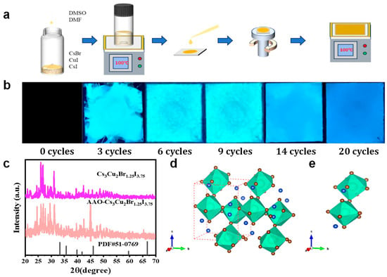
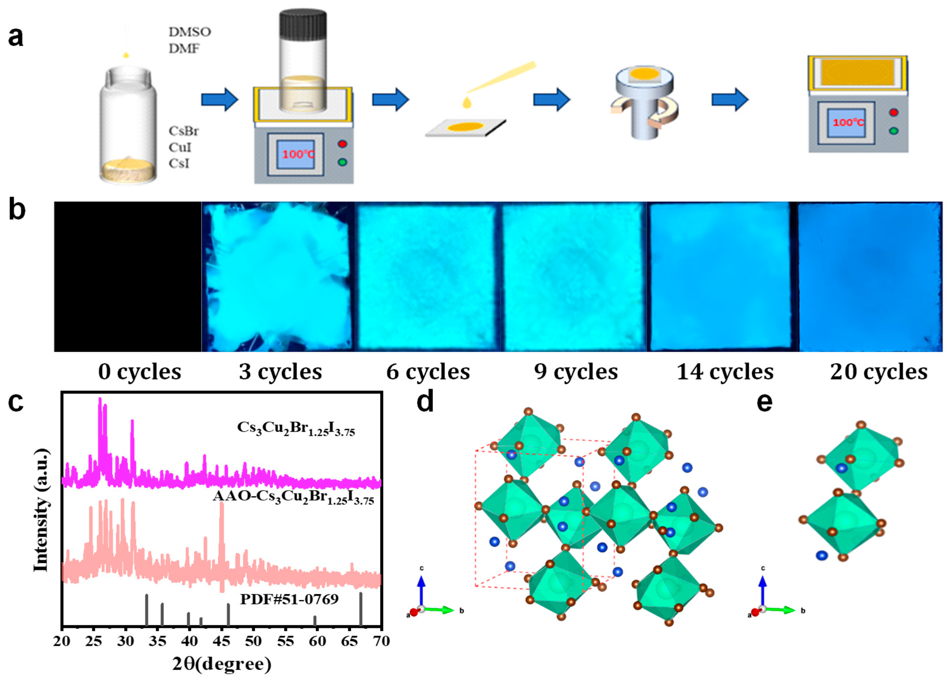
Figure 1a illustrates the in situ growth process of Cs3Cu2Br1.25I3.75 crystals within the AAO template. In the experiment, a pre-prepared precursor solution was uniformly spread onto the AAO surface through multiple spin-coating cycles, while the infiltration of the solution into the nanopores was mainly driven by capillary forces. Subsequent thermal treatment promoted gradual crystallization and the oriented arrangement of the crystals inside the template channels. As shown in Figure 1b, ultraviolet fluorescence images reveal that the surface distribution uniformity of Cs3Cu2Br1.25I3.75 crystals on the AAO template visibly improves with increasing spin-coating cycles. To further verify the crystal structure of the obtained material, Figure 1c presents the X-ray diffraction (XRD) pattern of the Cs3Cu2Br1.25I3.75-AAO film. All diffraction peaks arising from the evaporation-assisted crystallization process are consistent with those of Cs3Cu2Br1.25I3.75 powder prepared by the cooling crystallization method. In addition, several extra diffraction peaks corresponding to Al2O3 are observed, indicating that Cs3Cu2Br1.25I3.75 perovskite crystals were successfully grown in situ within the AAO membrane. Figure 1d,e shows the crystal structure analysis, which demonstrates that Cs3Cu2Br1.25I3.75 and Cs3Cu2Br5 possess similar crystal structures [31,32]. The Cu ions occupy two distinct coordination environments, namely tetrahedral and trigonal sites, forming two different structural units. These units are interconnected through the sharing of two halide ions, while Cs ions are located between the polyhedral units, separating the structural frameworks.
Figure 1.
(a) In situ growth process of Cs3Cu2Br1.25I3.75 crystals within an anodic aluminum oxide (AAO) template; (b) Growth behavior of Cs3Cu2Br1.25I3.75 in the AAO template under different spin-coating cycles; (c) X-ray diffraction (XRD) pattern of the Cs3Cu2Br1.25I3.75-AAO film; (d) Crystal structure of Cs3Cu2Br1.25I3.75:Blue spheres represent Cs+ cations, brown spheres denote disordered halogen sites occupied by Br−and I− ions, green polyhedra indicate the Cu2+ coordination environment, and the red dashed frame outlines a single unit cell; (e) Cs3Cu2Br1.25I3.75 smallest structural unit.
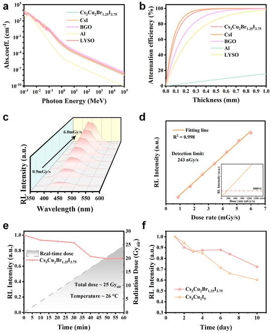
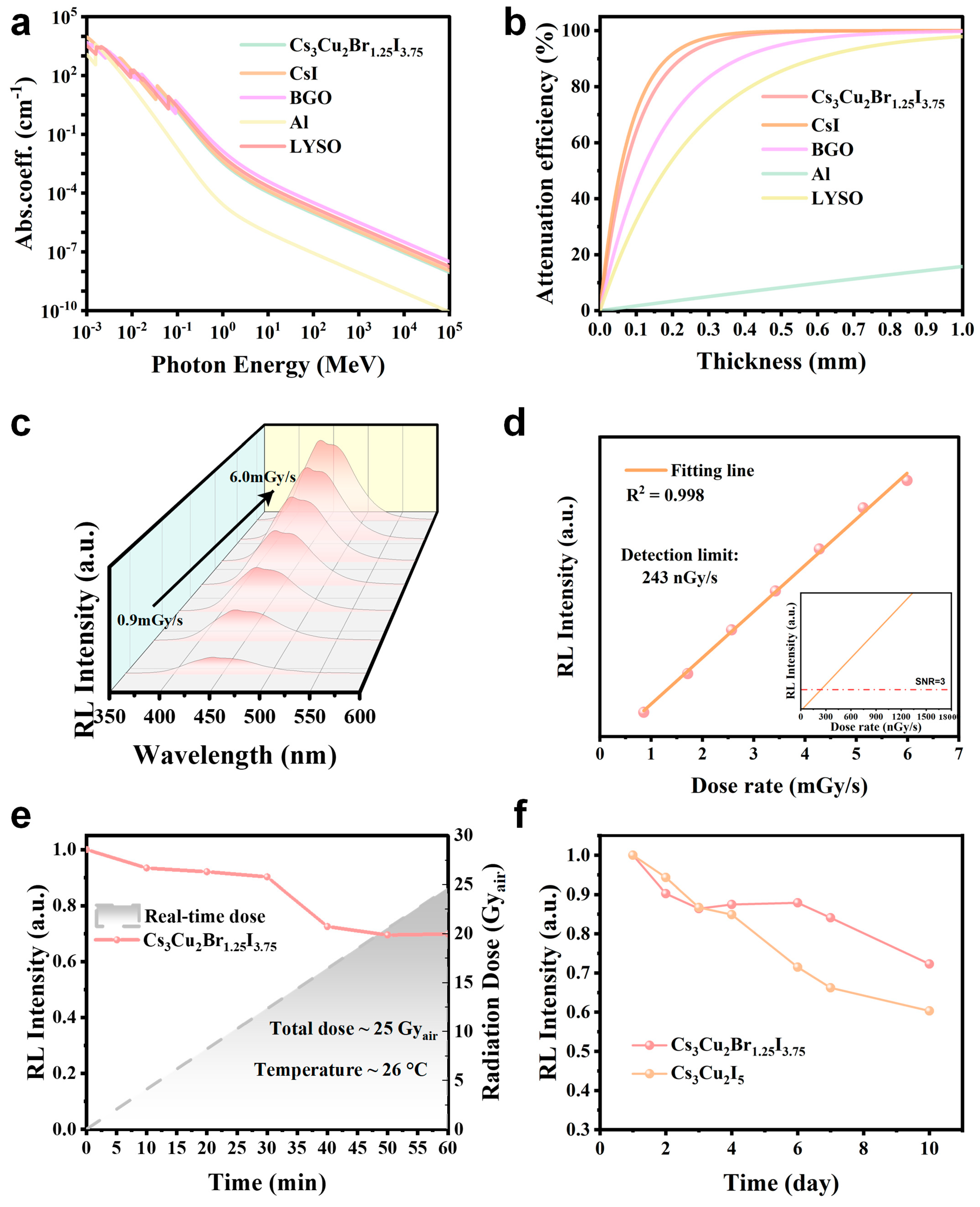
The X-ray absorption capability of a scintillator directly determines its detection efficiency and luminescence performance and is therefore considered one of the key parameters for evaluating scintillator materials [33]. By utilizing photon cross-section databases (the NIST XCOM database), we systematically compared the X-ray absorption properties of Cs3Cu2Br1.25I3.75 with those of commercially available scintillators, as shown in Figure 2a. The results indicate that Cs3Cu2Br1.25I3.75 exhibits absorption performance comparable to, or even competitive with, that of commercial scintillators such as CsI: Tl, BGO, and LYSO over the entire X-ray energy range. It is worth noting that the contribution of the Al substrate at the bottom of the AAO template to X-ray absorption is negligible, which was further confirmed by additional calculations.
Figure 2.
(a) Comparison of the X-ray absorption coefficients of Cs3Cu2Br1.25I3.75 and representative scintillator materials at different photon energies; (b) X-ray attenuation efficiency as a function of material thickness, calculated using linear attenuation coefficients at a photon energy of 50 keV, demonstrating the radiation shielding performance under this energy condition; (c) Radioluminescence (RL) intensity responses under different X-ray dose rates; (d) Linear relationship between RL intensity and dose rate (R2 = 0.998), with a detection limit of 243 nGy/s (inset: linear fitting in the low-dose region); (e) RL stability under a total accumulated dose of approximately 25 Gy/air; (f) RL intensity for Cs3Cu2Br1.25I3.75-AAO and Cs3Cu2I5 under ambient conditions over 10 days.
Furthermore, experimental measurements show that a Cs3Cu2Br1.25I3.75 sample with a thickness of 400 μm can effectively attenuate 50 keV X-rays, achieving nearly complete absorption of the incident radiation, as illustrated in Figure 2b. In contrast, an Al substrate with the same thickness exhibits much weaker attenuation capability, indicating that the presence of the Al substrate does not introduce a significant influence during practical imaging processes. Figure 2c presents the X-ray-excited radioluminescence (RL) spectra of the Cs3Cu2Br1.25I3.75-AAO film under different radiation dose rates. The integrated RL intensity as a function of dose rate was further extracted, as shown in Figure 2d. A good linear response is maintained even at a dose rate as low as 6 mGy/s, which excludes the contribution from defect-related emission. In addition, the minimum detectable dose rate of the Cs3Cu2Br1.25I3.75-AAO scintillator was evaluated. At a signal-to-noise ratio (SNR) of 3, the detection limit was determined to be 243 nGy/s, which is significantly lower than the typical dose rate (~5.5 μGy/s) required for medical X-ray diagnostic imaging, as reported in the literature [34].
To comprehensively evaluate the practical application potential of Cs3Cu2Br1.25I3.75-AAO, its stability under continuous X-ray irradiation was systematically investigated. As shown in Figure 2e, the Cs3Cu2Br1.25I3.75-AAO composite exhibits excellent radiation tolerance under continuous exposure to 50 keV X-rays. After more than 1 h of irradiation, corresponding to a cumulative dose exceeding 25 Gy/air, the integrated RL intensity remains at approximately 70% of its initial value. These results demonstrate the reliability and durability of Cs3Cu2Br1.25I3.75-AAO in practical applications, particularly for imaging scenarios requiring sub-second exposure times, where the performance exceeds current application requirements [35]. Figure 2f shows the RL intensity evolution of the Cs3Cu2Br1.25I3.75-AAO material under ambient conditions over a period of 10 days. During one week of natural storage, the RL intensity remains above 70% of its initial value. In comparison, undoped Cs3Cu2I5 single crystals exhibit a decrease to approximately 60% within one week [22], indicating that Cs3Cu2Br1.25I3.75-AAO displays superior RL stability.
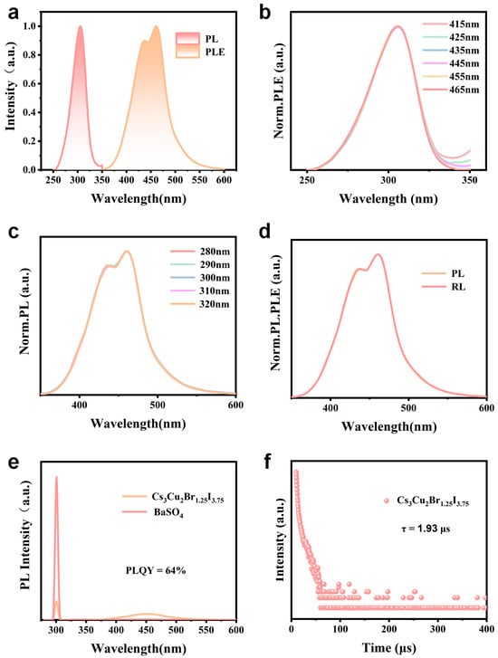
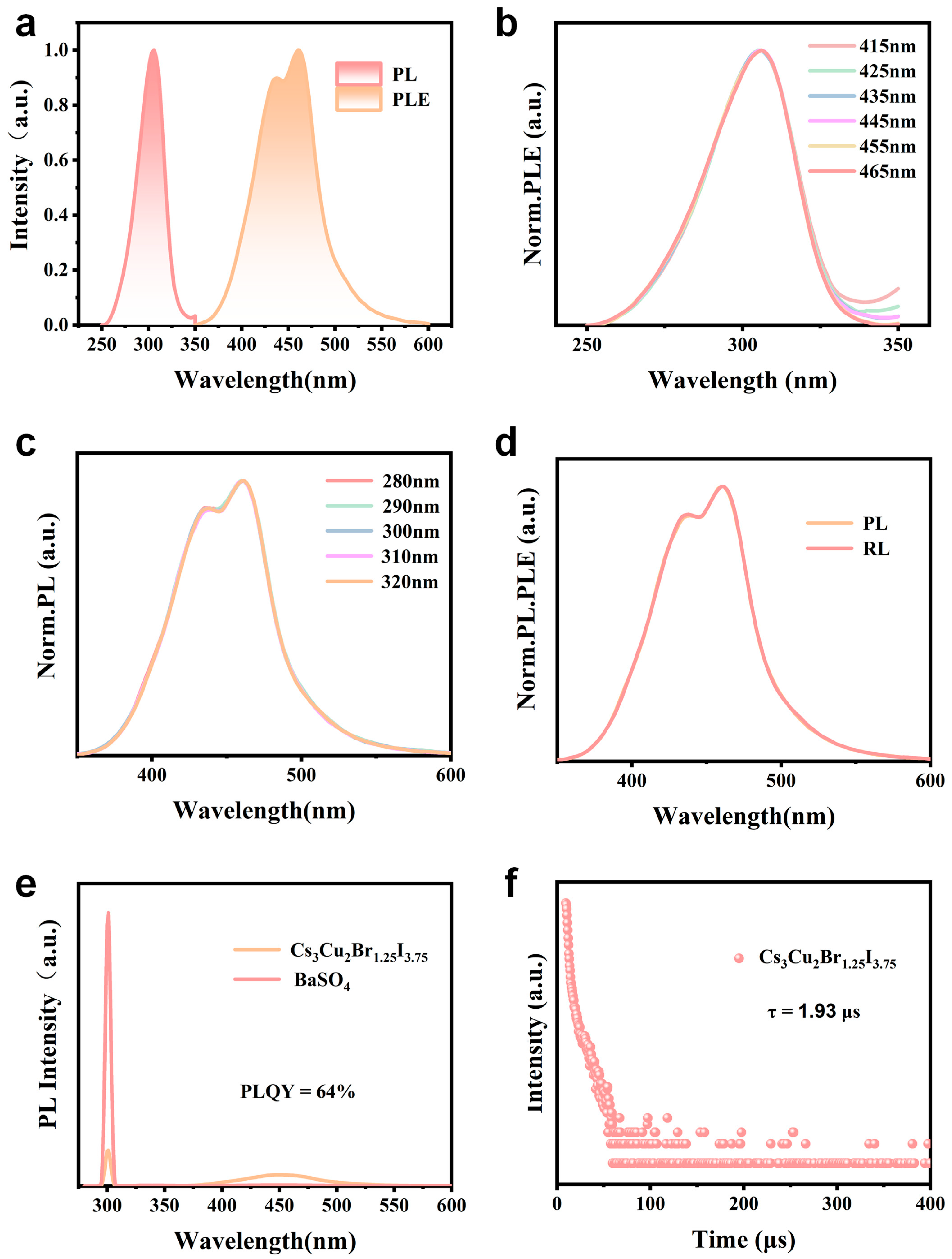
Figure 3a shows the photoluminescence excitation (PLE) and photoluminescence (PL) spectra of the synthesized Cs3Cu2Br1.25I3.75-AAO. Under excitation at 307 nm, a bright blue emission peak centered at 437 nm is observed for Cs3Cu2Br1.25I3.75-AAO. The emission exhibits a full width at half maximum (FWHM) exceeding 90 nm and a large Stokes shift of approximately 130 nm, which is characteristic of self-trapped exciton (STE) emission. Notably, there is negligible spectral overlap between the excitation and emission spectra, indicating minimal self-absorption behavior. To further investigate the emission characteristics, PL spectra were recorded under different excitation wavelengths, and PLE spectra were collected at different emission wavelengths. As shown in Figure 3b,c, Cs3Cu2Br1.25I3.75-AAO was excited using wavelengths ranging from 280 to 320 nm, resulting in multiple PL spectra. After normalization, these PL spectra nearly overlap, exhibiting identical peak positions and spectral widths. This behavior indicates that the position and shape of the emission band remain unchanged as the excitation wavelength varies within the 280–320 nm excitation range. In addition, PLE spectra were recorded by monitoring emission wavelengths from 405 to 465 nm. After normalization, the PLE spectra also show nearly identical peak positions and bandwidths. Furthermore, as shown in Figure 3d, the normalized PL and radioluminescence (RL) spectra overlap well, suggesting that the excited charge carriers undergo a single radiative recombination pathway. This observation implies that the entire emission band originates from the same dynamic process. Unlike three-dimensional perovskite structures, these zero-dimensional structures based on isolated [Cu2X5]3− units exhibit strong electron-phonon coupling and pronounced exciton localization. Consequently, they give rise to broadband emission with a large Stokes shift induced by STEs. These features, including the broad emission bandwidth and large Stokes shift, are fully consistent with the spectral characteristics observed in this work.
Figure 3.
(a) Photoluminescence (PL) and photoluminescence excitation (PLE) spectra of Cs3Cu2Br1.25I3.75-AAO; (b) PLE spectra of Cs3Cu2Br1.25I3.75-AAO recorded at various emission wavelengths ranging from 405 to 465 nm; (c) PL spectra of Cs3Cu2Br1.25I3.75-AAO under excitation wavelengths from 280 to 320 nm; (d) Normalized PL and radioluminescence (RL) spectra of Cs3Cu2Br1.25I3.75-AAO; (e) Absolute photoluminescence intensity of Cs3Cu2Br1.25I3.75 measured using an integrating sphere system with BaSO4 as the diffuse reflectance standard. (f) Time-resolved photoluminescence spectra of Cs3Cu2Br1.25I3.75-AAO.
Furthermore, the luminescence efficiency and emission dynamics of the Cs3Cu2Br1.25I3.75-AAO array were systematically characterized. As shown in Figure 3e, the absolute photoluminescence intensity was measured using an integrating sphere system with BaSO4 as the reference material, and the corresponding photoluminescence quantum yield (PLQY) was determined to be 64%. This result indicates a high radiative efficiency during the excited-state recombination process and further confirms the effectiveness and dominant role of the self-trapped exciton (STE) radiative recombination pathway. Figure 3f presents the time-resolved photoluminescence decay curve under pulsed excitation. By fitting the decay profile with a single-exponential function, a photoluminescence lifetime (τ) of 1.93 μs was obtained, which is characteristic of microsecond-scale emission associated with STEs. Overall, Cs3Cu2Br1.25I3.75-AAO exhibits pronounced STE-dominated emission behavior, high quantum efficiency, and well-defined emission dynamics, thereby providing a solid foundation for its application in high-resolution, low-dose X-ray imaging.
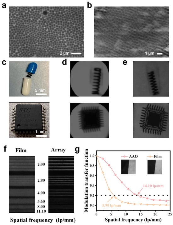
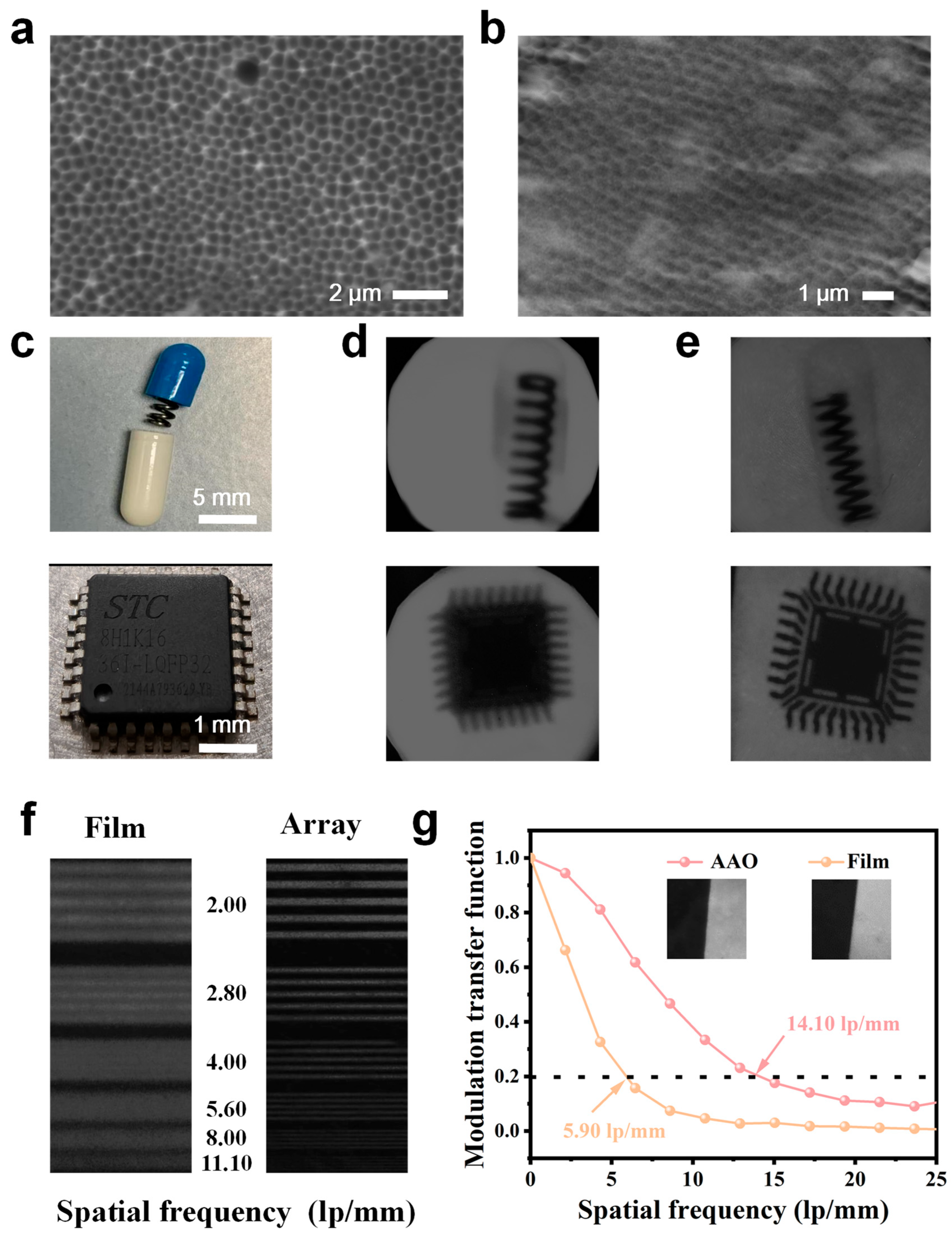
Figure 4a,b show scanning electron microscopy (SEM) images of the pristine AAO template and the surface of the Cs3Cu2Br1.25I3.75-AAO array, respectively. It can be observed that, through the spatially confined evaporation-assisted crystallization process, the Cs3Cu2Br1.25I3.75 precursor solution enables successful in situ growth of arrayed nanocrystals within the AAO pores. The resulting arrays exhibit a regular arrangement and uniform pore size, indicating good reproducibility of the template-guided growth process. To evaluate the imaging performance, X-ray imaging experiments were carried out using a 35 keV X-ray source to irradiate test objects containing internal structures, and the scintillation images were recorded with a digital camera. The test objects included opaque capsules containing internal springs and 5 mm chips. Figure 4c presents photographs of representative test objects, such as the spring and the chip. Figure 4d,e display the X-ray images obtained using a conventional film-type Cs3Cu2Br1.25I3.75 scintillator (Cs3Cu2Br1.25I3.75-Film) and the array-structured Cs3Cu2Br1.25I3.75-AAO scintillator, respectively. Although both scintillators are capable of resolving the internal information of the test objects, a clear comparison reveals that the array-structured Cs3Cu2Br1.25I3.75-AAO produces images with higher clarity and sharper edges. The spatial resolution was first evaluated using images of a standard line-pair phantom, as shown in Figure 4f. The Cs3Cu2Br1.25I3.75-AAO scintillator achieves a spatial resolution of 11.10 lp/mm, representing a significant improvement compared with the resolution of 4.00 lp/mm obtained for the Cs3Cu2Br1.25I3.75-Film. Further quantitative analysis was performed using the standard slanted-edge method. As shown in Figure 4g, at a modulation transfer function (MTF) value of 0.2, the spatial resolutions of Cs3Cu2Br1.25I3.75-Film and Cs3Cu2Br1.25I3.75-AAO are determined to be 5.90 lp/mm and 14.10 lp/mm, respectively. These imaging results indicate that the AAO nanoporous array structure, by providing enhanced optical confinement and suppressing lateral scintillation photon spreading, plays a dominant role in improving spatial resolution and edge sharpness, rather than changes in the intrinsic scintillation properties of Cs3Cu2Br1.25I3.75 itself.
Figure 4.
(a) SEM image of the surface of the pristine AAO template; (b) SEM image of the surface of the Cs3Cu2Br1.25I3.75-AAO scintillator; (c) Photographs of the test objects (spring and chip); (d) X-ray imaging result obtained using the Cs3Cu2Br1.25I3.75-Film scintillator; (e) X-ray imaging result obtained using the Cs3Cu2Br1.25I3.75-AAO scintillator; (f) Modulation transfer function (MTF) curve measured using the standard slanted-edge method for the Cs3Cu2Br1.25I3.75-Film scintillator; the inset shows the corresponding slanted-edge image and the imaging result of a standard X-ray resolution test card obtained with the Cs3Cu2Br1.25I3.75-AAO scintillator; (g) Modulation transfer function (MTF) curves of Cs3Cu2Br1.25I3.75-AAO and Cs3Cu2Br1.25I3.75-Film scintillators, where the black dashed line represents the MTF = 0.2 threshold for defining limiting spatial resolution (inset: corresponding slanted-edge image).
4. Conclusions
In this study, a spatially confined evaporation-assisted crystallization strategy was proposed and demonstrated to enable the in situ growth of Cs3Cu2Br1.25I3.75 nanoarray scintillators within anodic aluminum oxide (AAO) templates. Leveraging the high ordering, uniform pore dimensions, and good processability of the AAO template, Cs3Cu2Br1.25I3.75 was grown in an arrayed manner within nanoscale pores. The resulting arrayed scintillator exhibits a photoluminescence quantum yield of 62% and a microsecond-scale lifetime of 1.93 μs. The emission process is dominated by self-trapped excitons (STEs), characterized by a large Stokes shift and broadband emission, which is favorable for efficient radiative recombination and reduced optical crosstalk in imaging applications.
Under X-ray excitation, the Cs3Cu2Br1.25I3.75-AAO array demonstrates strong imaging performance, achieving a spatial resolution of 14.10 lp/mm and a low detection limit of 243 nGy/s, exceeding the performance reported for most lead-free perovskite-based scintillators. Compared with conventional thick-film Cs3Cu2Br1.25I3.75 scintillators, the arrayed structure shows clear advantages in image sharpness, contrast, and fine-detail resolution. These improvements are primarily attributed to the longitudinal optical waveguiding effect and lateral optical isolation between adjacent pixels provided by the AAO template, which effectively reduces lateral photon diffusion and signal crosstalk. In addition, the Cs3Cu2Br1.25I3.75-AAO scintillator exhibits good environmental and radiation stability, maintaining a high luminescence intensity under prolonged high-dose X-ray irradiation and during storage under ambient conditions. These results indicate its practical feasibility for real-world applications. Overall, the Cs3Cu2Br1.25I3.75-AAO array scintillator shows strong potential for high-resolution, low-dose X-ray imaging and provides a viable strategy for the development of cost-effective and structurally controllable scintillation screens.
Author Contributions
Conceptualization, X.L. and T.L.; methodology, X.L.; software, X.L., Z.Y. and B.Z.; validation, X.L., J.H. and Z.Z.; formal analysis, X.L.; investigation, X.L., Z.Y. and B.Z.; resources, T.L.; data curation, X.L., B.Z. and Z.Y.; writing—original draft preparation, X.L.; writing—review and editing, X.L. and T.L.; supervision, T.L.; project administration, T.L. All authors have read and agreed to the published version of the manuscript.
Funding
The Guangxi Natural Science Foundation (Nos. 2025GXNSFAA069543, 2025GXNSFAA069357) and the National Natural Science Foundation of China (No. 52472153).
Data Availability Statement
The original contributions presented in this study are included in the article. Further inquiries can be directed to the corresponding author.
Acknowledgments
During the preparation of this manuscript, the authors used ChatGPT (OpenAI, GPT-5.2) [M1.1] for language polishing and improvement of academic expression only. The scientific content, experimental design, data analysis, results, and conclusions were entirely developed and verified by the authors. The authors take full responsibility for the integrity and originality of this work.
Conflicts of Interest
The authors declare no conflicts of interest.
References
- Ou, X.; Chen, X.; Xu, X.; Xie, L.; Chen, X.; Hong, Z.; Bai, H.; Liu, X.; Chen, Q.; Li, L.; et al. Recent Development in X-Ray Imaging Technology: Future and Challenges. Research 2021, 2021, 9892152. [Google Scholar] [CrossRef] [Scilit] [PubMed]
- Pang, J.; Wu, H.; Li, H.; Jin, T.; Tang, J.; Niu, G. Reconfigurable perovskite X-ray detector for intelligent imaging. Nat. Commun. 2024, 15, 1769. [Google Scholar] [CrossRef] [Scilit]
- Sakhatskyi, K.; Turedi, B.; Matt, G.J.; Wu, E.; Sakhatska, A.; Bartosh, V.; Lintangpradipto, M.N.; Naphade, R.; Shorubalko, I.; Mohammed, O.F.; et al. Stable perovskite single-crystal X-ray imaging detectors with single-photon sensitivity. Nat. Photonics 2023, 17, 510–517. [Google Scholar] [CrossRef] [Scilit]
- Wang, J.-X.; Shekhah, O.; Bakr, O.M.; Eddaoudi, M.; Mohammed, O.F. Energy transfer-based X-ray imaging scintillators. Chem 2025, 11, 102273. [Google Scholar] [CrossRef] [Scilit]
- Li, H.; Wang, C.-f.; Luo, Q.-f.; Ma, C.; Zhang, J.; Zhao, R.; Yang, T.; Du, Y.; Chen, X.; Li, T.; et al. Wearable Photoferroelectric Perovskite X-Ray Detectors. Adv. Funct. Mater. 2024, 34, 2407693. [Google Scholar] [CrossRef] [Scilit]
- Spahn, M. X-ray detectors in medical imaging. Nucl. Instrum. Methods Phys. Res. Sect. A Accel. Spectrometers Detect. Assoc. Equip. 2013, 731, 57–63. [Google Scholar] [CrossRef] [Scilit]
- Zentai, G.; Partain, L.; Pavlyuchkova, R.; Proano, C.; Schieber, M.; Shah, K.; Bennett, P. Comparison of mercuric iodide and lead iodide X-ray detectors for X-ray imaging applications. In Proceedings of the Nuclear Science Symposium/Medical Imaging Conference, Rome, Italy, 16–22 October 2004; pp. 2278–2282. [Google Scholar]
- Cha, B.K.; Jeon, S.; Lee, M.; Lee, H.; Cho, H.; Seo, C.W. Design and performance evaluation of different high-resolution scintillators in digital X-ray imaging detector. Nucl. Instrum. Methods Phys. Res. Sect. A Accel. Spectrometers Detect. Assoc. Equip. 2024, 1063, 169323. [Google Scholar] [CrossRef] [Scilit]
- He, G.L.; Li, L.J.; Chen, J.Y.; Gong, Y.J.; Guo, H. An efficient Cu+ doped Gd-based fluoroaluminosilicate scintillator glass for X-ray detectors. J. Mater. Chem. C 2025, 13, 1325–1331. [Google Scholar] [CrossRef] [Scilit]
- Wu, Z.; Jia, W.; Wu, Y.; Hei, D.; Sun, A.; Ling, Y.; Shan, Q.; Shi, C.; Zhang, J. Design of a five-layers multi-energy X-ray imaging detector for material sorting. Appl. Radiat. Isot. 2023, 194, 110711. [Google Scholar] [CrossRef] [Scilit] [PubMed]
- Yang, L.; Li, Z.; He, L.; Sun, J.; Wang, J.; Wang, Y.; Li, M.; Zhu, Z.; Dai, X.; Hu, S.; et al. Emergence of a Lanthanide Chalcogenide as an Ideal Scintillator for a Flexible X-ray Detector. Angew. Chem. Int. Ed. 2023, 62, e202306465. [Google Scholar] [CrossRef] [Scilit] [PubMed]
- Zhang, Q.; Zhang, S.; Zheng, R.; Du, P.; Ding, J.; Wei, W. High-efficiency narrow-band green-emitting Tb-doped fluorosilicate glass for X-ray detectors. J. Non Cryst. Solids 2023, 608, 122236. [Google Scholar] [CrossRef] [Scilit]
- Han, M.; Xiao, Y.; Zhou, C.; Yang, Y.; Wu, X.; Hu, Q.; Jin, X.; Zhang, W.; Hu, J.-S.; Jiang, Y. Recent advances on two-dimensional metal halide perovskite x-ray detectors. Mater. Futures 2023, 2, 012104. [Google Scholar] [CrossRef] [Scilit]
- Wang, B.; Yang, X.; Li, R.; Qaid, S.M.H.; Cai, W.; Xiao, H.; Zang, Z. One-Dimensional CsCu2I3 Single-Crystal X-ray Detectors. ACS Energy Lett. 2023, 8, 4406–4413. [Google Scholar] [CrossRef] [Scilit]
- Wang, W.; Cai, M.; Liu, X.; Ji, K.; Yu, X.; Dai, S. Metal halide perovskite single crystal growth and application for X-ray detectors. J. Mater. Chem. C 2023, 11, 12105–12127. [Google Scholar] [CrossRef] [Scilit]
- Hao, X.; Nie, L.; Zhu, X.; Zeng, G.; Liu, C.; Teng, Z.; Liu, H.; Yue, Y.; Yu, X.; Wang, T. High-Resolution X-ray Image from Copper-Based Perovskite Hybrid Polymer. ACS Appl. Mater. Interfaces 2024, 16, 29210–29216. [Google Scholar] [CrossRef] [Scilit]
- Zhou, W.; Zhu, X.; Yu, J.; Mou, D.; Li, H.; Kong, L.; Lang, T.; Peng, L.; Chen, W.; Xu, X.; et al. High-Quality Cs3Cu2I5@PMMA Scintillator Films Assisted by Multiprocessing for X-ray Imaging. ACS Appl. Mater. Interfaces 2023, 15, 38741–38749. [Google Scholar] [CrossRef] [Scilit]
- Han, L.; Zhao, J.; Miao, Y.; Zhou, W.; Yuan, M.; Cui, J.; Ci, Z. Thermal stability and flexible X-Ray scintillation screen through in-situ assembling Cs3Cu2Cl5 nanocrystals in polymer matrix. Mater. Res. Bull. 2024, 179, 112980. [Google Scholar] [CrossRef] [Scilit]
- Xiang, W.; Shen, D.; Zhang, X.; Li, X.; Liu, Y.; Zhang, Y. Transparent and Planar Cs3Cu2Cl5 Crystals for Micrometer-Resolution X-ray Imaging Screen. ACS Appl. Mater. Interfaces 2024, 16, 4918–4924. [Google Scholar] [CrossRef] [Scilit]
- Roccanova, R.; Yangui, A.; Nhalil, H.; Shi, H.; Du, M.-H.; Saparov, B. Near-Unity Photoluminescence Quantum Yield in Blue-Emitting Cs3Cu2Br5–xIx (0 ≤ x ≤ 5). ACS Appl. Electron. Mater. 2019, 1, 269–274. [Google Scholar] [CrossRef] [Scilit]
- Ren, Y.; Lü, S. Industrial mass production of novel mixed-halide Cs3Cu2Cl5-xIx and Cs5Cu3Cl8-xIx compounds with greatly enhanced stability and luminescent efficiency by compositional engineering. Chem. Eng. J. 2021, 417, 129223. [Google Scholar] [CrossRef] [Scilit]
- Liu, J.; Li, X.; Zhao, J.; Liu, H.; Lin, T. Efficient and stable Cs5Cu3Cl8-xIx (x = 1,2) single crystalline scintillators for X-ray imaging. J. Alloys Compd. 2025, 1021, 179659. [Google Scholar] [CrossRef] [Scilit]
- Zhao, B.-Z.; Qin, X.-B.; Feng, Z.-D.; Wei, C.-F.; Chen, Y.; Wang, B.-Y.; Wei, L. Performance evaluation of CsI screens for X-ray imaging. Chin. Phys. C 2014, 38, 116003. [Google Scholar] [CrossRef] [Scilit]
- Rocha, J.G.; Dias, R.A.; Goncalves, L.; Minas, G.; Ferreira, A.; Costa, C.M.; Lanceros-Mendez, S. X-Ray Image Detector Based on Light Guides and Scintillators. IEEE Sens. J. 2009, 9, 1154–1159. [Google Scholar] [CrossRef] [Scilit]
- Cha, B.K.; Kim, J.Y.; Cho, G.; Seo, C.-W.; Jeon, S.; Huh, Y. Quasi-pixel structured nanocrystalline Gd2O3 (Eu) scintillation screens and imaging performance for indirect X-ray imaging sensors. Nucl. Instrum. Methods Phys. Res. Sect. A Accel. Spectrometers Detect. Assoc. Equip. 2011, 648, S12–S15. [Google Scholar] [CrossRef] [Scilit]
- Shao, W.; He, T.; Wang, L.; Wang, J.-X.; Zhou, Y.; Shao, B.; Ugur, E.; Wu, W.; Zhang, Z.; Liang, H.; et al. Capillary Manganese Halide Needle-Like Array Scintillator with Isolated Light Crosstalk for Micro-X-Ray Imaging. Adv. Mater. 2024, 36, 2312053. [Google Scholar] [CrossRef] [Scilit]
- Wang, S.; Gu, Z.; Zhao, R.; Zhang, T.; Lou, Y.; Guo, L.; Su, M.; Li, L.; Zhang, Y.; Song, Y. A general method for growth of perovskite single-crystal arrays for high performance photodetectors. Nano Res. 2022, 15, 6568–6573. [Google Scholar] [CrossRef] [Scilit]
- Hui, J.; Ran, P.; Su, Y.; Yang, L.; Xu, X.; Liu, T.; Yang, Y.M. High-Resolution X-ray Imaging Based on Solution-Phase-Synthesized Cs3Cu2I5 Scintillator Nanowire Array. J. Phys. Chem. C 2022, 126, 12882–12888. [Google Scholar] [CrossRef] [Scilit]
- Liang, D.; Tan, L.; Lu, S.; Sun, Z.; Wang, H.; Cai, W.; Zang, Z. Low-Temperature Solution Synthesis of Stable Cs3Cu2Br5 Single Crystals for Visible Light Communications. ACS Appl Mater Interfaces 2023, 15, 24622–24628. [Google Scholar] [CrossRef] [Scilit]
- Jun, T.; Sim, K.; Iimura, S.; Sasase, M.; Kamioka, H.; Kim, J.; Hosono, H. Lead-Free Highly Efficient Blue-Emitting Cs3Cu2I5 with 0D Electronic Structure. Adv. Mater. 2018, 30, 1804547. [Google Scholar] [CrossRef] [Scilit]
- Zeng, B.; Liu, Y.; Bao, S.; Wang, C.; Xu, R.; Liu, J.; Zhu, Y. The growth of Cs3Cu2Br5 and CsCu2Br3 single crystals by cooling crystallization for scintillator application. Crystengcomm 2025, 27, 2888–2894. [Google Scholar] [CrossRef] [Scilit]
- Zheng, X.; Huang, J.; Liu, Y.; Wang, T.; Han, S.; Wang, Z.; Teng, B.; Ji, S. Stable Lead-Free Blue-Emitting Cs3Cu2Br5 Single Crystal with Self-Trap Exciton Emission for Optoelectronics. Adv. Photonics Res. 2022, 3, 2100289. [Google Scholar] [CrossRef] [Scilit]
- Yanagida, T. Inorganic scintillating materials and scintillation detectors. Proc. Jpn. Acad. Ser. B 2018, 94, 75–97. [Google Scholar] [CrossRef] [Scilit] [PubMed]
- Clairand, I.; Bordy, J.M.; Carinou, E.; Daures, J.; Debroas, J.; Denozière, M.; Donadille, L.; Ginjaume, M.; Itié, C.; Koukorava, C.; et al. Use of active personal dosemeters in interventional radiology and cardiology: Tests in laboratory conditions and recommendations—ORAMED project. Radiat. Meas. 2011, 46, 1252–1257. [Google Scholar] [CrossRef] [Scilit]
- Yanagida, T.; Kato, T.; Nakauchi, D.; Kawaguchi, N. Fundamental aspects, recent progress and future prospects of inorganic scintillators. Jpn. J. Appl. Phys. 2023, 62, 010508. [Google Scholar] [CrossRef] [Scilit]
Disclaimer/Publisher’s Note: The statements, opinions and data contained in all publications are solely those of the individual author(s) and contributor(s) and not of MDPI and/or the editor(s). MDPI and/or the editor(s) disclaim responsibility for any injury to people or property resulting from any ideas, methods, instructions or products referred to in the content. |
© 2026 by the authors. Licensee MDPI, Basel, Switzerland. This article is an open access article distributed under the terms and conditions of the Creative Commons Attribution (CC BY) license.