


Abstract
This paper examines the impact of defect-related Density of States (DOS) on both dark and illuminated conductivity of intrinsic amorphous silicon (a-Si:H). The quality of the a-Si:H layer plays a crucial role in achieving high photovoltaic (PV) conversion efficiency, especially when it functions as the absorber layer between two heavily doped regions. Extensive studies have demonstrated that common fabrication processes can introduce a high density of defect states within the bandgap. These defects are typically modeled using two exponentially decaying distributions to represent the valence- and conduction-band tails (BTs), along with two correlated Gaussian distributions accounting for deep defect states associated with dangling bonds (DBs). Based on this model, numerical simulations are carried out by solving the fundamental semiconductor equations—namely Poisson’s equation and the electron and hole continuity equations—in order to analyze how DOS defects affect and govern the electrical conductivity of a-Si:H.
1. Introduction
Technologically transformative materials are rare, as they require distinctive electronic and structural properties that clearly differentiate them from established materials. Amorphous silicon (a-Si:H) represents a notable example of such innovation, with widespread applications in photovoltaics and large-area electronic device arrays. Rather than being regarded merely as a degraded form of crystalline silicon, its structural disorder is now understood to generate unique energy states and distinctive optoelectronic properties.
The development and technological maturation of hydrogenated amorphous silicon (a-Si:H) were enabled by the advent of plasma-enhanced chemical vapor deposition (PECVD) techniques where silane gas (SiH4) is decomposed in RF or DC glow discharges [1,2,3,4,5]. This method facilitates hydrogen incorporation, which passivates dangling bonds and stabilizes the disordered network, leading to the high-quality a-Si:H widely used today [6,7]. Despite these advances, a comprehensive understanding of its electrical conductivity and extended-state transport mechanisms remains a significant challenge [8].
Recent studies have continued to investigate the role of structural disorder, hydrogen incorporation, defect formation, and charge transport in a-Si:H, highlighting the strong relationship between material structure and its electrical and optoelectronic properties [9,10,11].
The electronic properties of a-Si:H are strongly governed by the Density of States (DOS) within the mobility gap, which consists of band-tail states and dangling bond (DB) defects. While numerous DOS-based simulation studies have successfully reproduced the electrical characteristics of a-Si:H devices [10,12], they generally employ fixed defect-state distributions and focus on the overall device performance. Consequently, the individual influence of the dangling bond distribution parameters on the conductivity of intrinsic a-Si has received comparatively less attention. Recent experimental investigations have provided further evidence of the importance of native and metastable gap states and their contribution to photoconductivity and charge transport. In particular, studies based on photoconductivity measurements have demonstrated the presence of different defect-state distributions within the mobility gap of intrinsic a-Si:H [13].
The effects of hydrogenation and light-induced defect formation on charge transport and photoconductivity have also been investigated in recent studies [10,13]. These results further emphasize the importance of understanding the relationship between defect-state distributions and the electrical properties of intrinsic a-Si:H.
This paper aims to provide a detailed numerical investigation of the conductivity behavior of intrinsic a-Si:H under both dark and illuminated conditions by systematically analyzing the influence of the dangling bond density, energy correlation, and Gaussian standard deviation, while keeping the band-tail distributions unchanged. This approach makes it possible to isolate the specific contribution of dangling bond states to carrier transport and electrical conductivity.
Our analysis is carried out using a computational model developed by the authors, based on the one-dimensional self-consistent numerical solution of Poisson’s equation and the electron and hole continuity equations using the Scharfetter–Gummel discretization scheme [14]. The implemented model incorporates the complete DOS distribution and its associated recombination mechanisms, enabling a comprehensive evaluation of the relationship between defect-state characteristics and the dark and photo-induced conductivity of intrinsic a-Si:H.
2. Modeling Description
The modeling of semiconductor devices involves solving the fundamental transport equations, namely the electron and hole continuity equations, together with Poisson’s equation. These equations are formulated as presented in Table 1, taking into account both the optical generation rate (Gopt) and the trap state density (NT). The free carrier concentrations in amorphous silicon are evaluated using the Maxwell–Boltzmann approximation, which is justified by the fact that the quasi-Fermi levels remain consistently more than three kT away from their respective band edges.
Table 1.
Summary of Poisson’s equation and hole (electron) continuity equations [14].
Gopt represents the generation of electron–hole pairs due to the absorption of incident solar radiation. It is calculated using the AM1.5 reference solar spectrum. It is equal to . Here, ϕi denotes the incident photon flux at wavelength i, while αi and Ri are the wavelength-dependent absorption and reflection coefficients of a-Si:H, respectively.
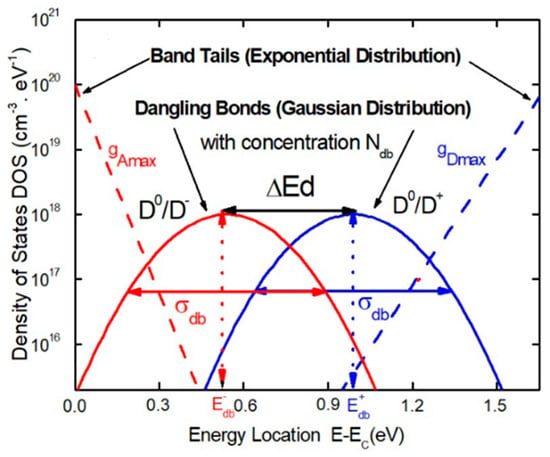
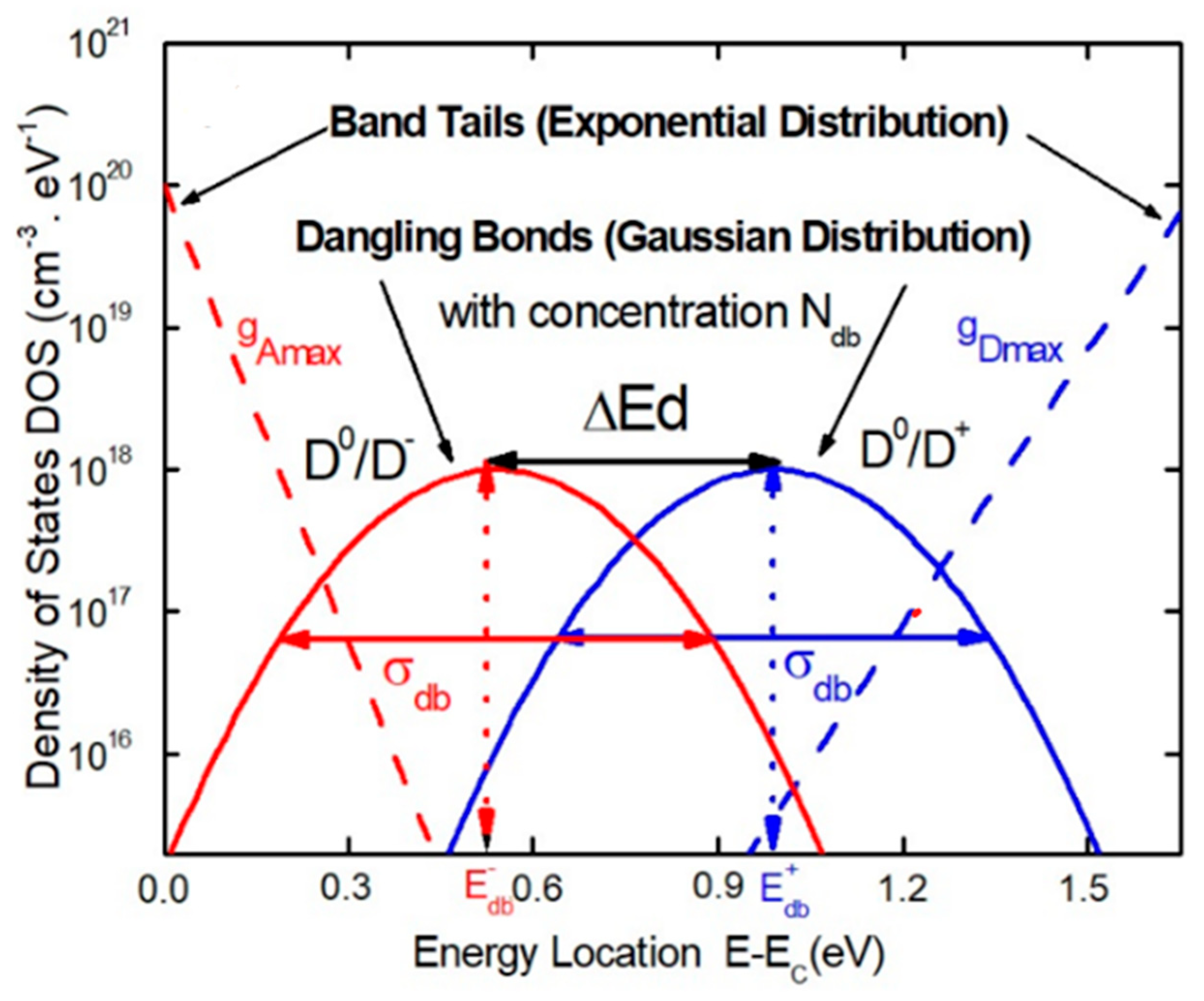
The trap state density NT, commonly described by the DOS, has a direct impact on the electrical behavior of the material. The usual DOS model in the amorphous silicon shown in Figure 1 is used to describe the U-shaped distribution of the states inside the forbidden bandgap [15,16].
Figure 1.
Density of States (DOS) in the bandgap of the a-Si:H.
The Density-of-States (DOS) model is composed of two main types of defect distributions, whose formulation is summarized in Table 2.
Table 2.
Summary of the bands tail (BT) and the dangling bond (DB) equations [17,18].
The band tails (BTs) are described by two exponentially decaying distributions extending into the bandgap from the valence and conduction bands.
Dangling bonds (DBs), originating from unsatisfied silicon–silicon bonds, are considered. These amphoteric defect centers behave as multi-level traps and are distributed over three energy levels corresponding to their possible charge states. In the standard DOS defect model, the energy distribution of dangling bond states is represented by a Gaussian function.
The total charge associated with these states is accounted for by NT, representing the volumetric charge density included in Poisson’s equation. A comprehensive description of the adopted DOS model, including its underlying assumptions, the selected DOS parameters, and the defect-state recombination mechanisms incorporated into the transport model included in the term Un (Up), is available in Refs [17,18].
3. Numerical Approach and Hypothesis
The system of three coupled nonlinear partial differential Equations (1)–(3) is solved using the finite difference method of Gummel:
- Each equation is solved independently for its main unknown: φ for Poisson’s equation, and φn or φp for the continuity equations.
- Each differential equation is approximated by a finite difference equation using a classical three-point scheme.
- Each equation of the system is represented as a matrix system with a tridiagonal structure.
- The solution to the linearized equations is obtained using the Gauss elimination method.
- Each solution is solved by turns and the iterative procedure runs until a chosen precision (10−6) is reached for the total conduction current.
- An adaptive mesh refinement procedure is used to ensure numerical accuracy. The mesh is refined (1 nm) near the two boundaries of the simulation domain, where the largest variations in the electrostatic potential and carrier concentrations occur, while a progressively coarser discretization is adopted toward the center of the domain. The spatial step is varied according to a geometric progression, providing a finer mesh near the boundaries and a coarser mesh in the central region, thereby reducing the computational cost while maintaining numerical accuracy. A similar adaptive/non-uniform meshing principle has been employed in numerical simulations of p-i-n structures and grain-boundary regions [19].
- The electrical boundary conditions are imposed at the two ends of the one-dimensional simulation domain. A Dirichlet boundary condition is applied at the first boundary (Va = 0.5 V), while an ohmic boundary condition is imposed at the other boundary.
- The simulated structure consists of a single intrinsic a-Si:H layer with a thickness of 300 nm, which is a representative thickness for the intrinsic absorber layer of a-Si:H p-i-n solar-cell structures ((200 nm–500 nm) [19].
- The simulation is performed at a temperature of 300 K under both dark and solar-illuminated conditions (AM1.5).
- The electrical conductivity is calculated from the simulated current density using the microscopic form of Ohm’s law, J = σ × E, where J is the current density (dark or illuminated conditions).
4. Simulation Parameters and Results
The objective of this study is to simulate the electrical conductivity of an intrinsic amorphous silicon (a-Si:H) layer, which acts as the absorber in p–i–n solar cells, under both dark and illuminated conditions. While previous studies have shown that band-tail states significantly influence transport properties in heavily doped layers, these states are neglected in the present work since the investigated layer is intrinsic. The analysis therefore focuses exclusively on the parameters governing dangling bond defect states.
Table 3 summarizes the physical and electrical parameters defining the a-Si:H layer that are kept constant throughout the simulations, along with the variation ranges of selected parameters. Particular emphasis is placed on the characteristics of dangling bond defects.
Table 3.
Physical and electrical parameters characterizing the a-Si:H [17,18].
The donor concentration of 1015 cm−3 represents a low residual/background donor concentration experimentally reported for nominally intrinsic a-Si:H [1,20]. It does not represent intentional doping and is therefore consistent with the use of the term “intrinsic” or “undoped” in the present study.
The selected values of the dangling bond density Ndb, correlation energy ΔEd, and Gaussian standard deviation σdb are representative of intrinsic PECVD-grown a-Si:H reported in previous experimental and numerical studies. The investigated parameter ranges were chosen to cover typical variations associated with differences in material quality, hydrogen passivation, and deposition conditions, while remaining within the physically realistic limits reported in the literature [1,17,18].
The simulation results presented below illustrate the impact of dangling bond defects on both electrical conductivity and the Fermi level under dark and illuminated conditions. These defects are characterized by key parameters, including their density, standard deviation, and correlation energy. The adopted methodology consists of varying one parameter at a time, while assigning selected values to a second parameter and keeping the third fixed at its reference value (see Table 3).
4.1. Dangling Bond Density Ndb Effect
Dangling bonds act as deep localized states within the bandgap and constitute efficient recombination centers [21]. Increasing the dangling bond density enhances the probability of carrier capture and recombination, thereby reducing the steady-state free carrier concentration. Consequently, the electrical conductivity decreases despite the increase in the total density of defect states. Conversely, under illumination, the conductivity enhancement results from the competition between photogenerated carrier generation and dangling bond-assisted recombination.
In the present study, the ratio of the electron and hole capture coefficients is fixed at Cn/Cp = 1 and the capture coefficients (for neutral, donor and acceptor dangling bond density) are not treated as independent variables. This assumption allows the analysis to focus specifically on the parameters governing the Gaussian distribution of dangling bond states.
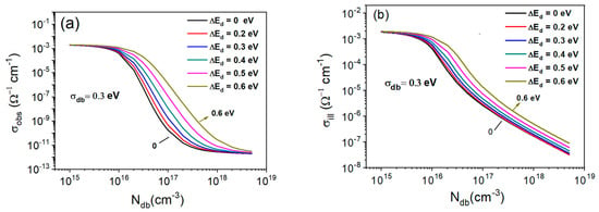
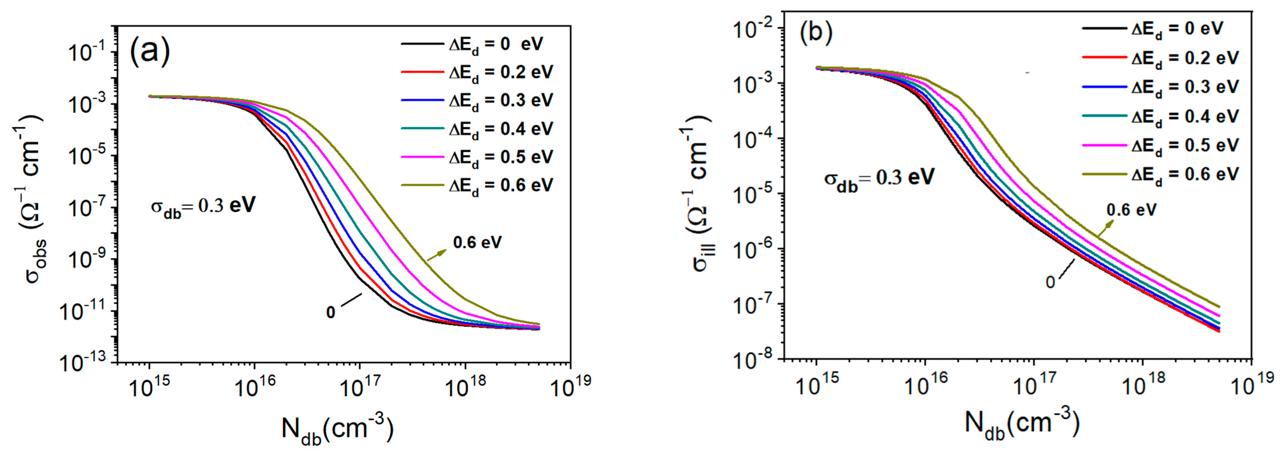
Figure 2 illustrates the variations in conductivity as a function of the dangling bond density Ndb ranging from 1015 cm−3 to 5 × 1018 cm−3 under both dark conditions (Figure 2a) and illumination (Figure 2b). The simulations are performed for different values of the correlation energy ΔEd (from 0 to 0.6 eV), while the standard deviation σdb is kept constant at its default value of 0.3 eV.
Figure 2.
Conductivity σ versus dangling bond density for different correlation energies ΔEd: (a) dark, (b) illuminated conditions.
The results clearly indicate that Ndb has a strong influence on conductivity. A significant decrease is observed for densities exceeding 1016 cm−3, with conductivity dropping by up to eight orders of magnitude in the dark and four orders of magnitude under illumination.
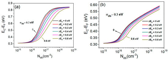
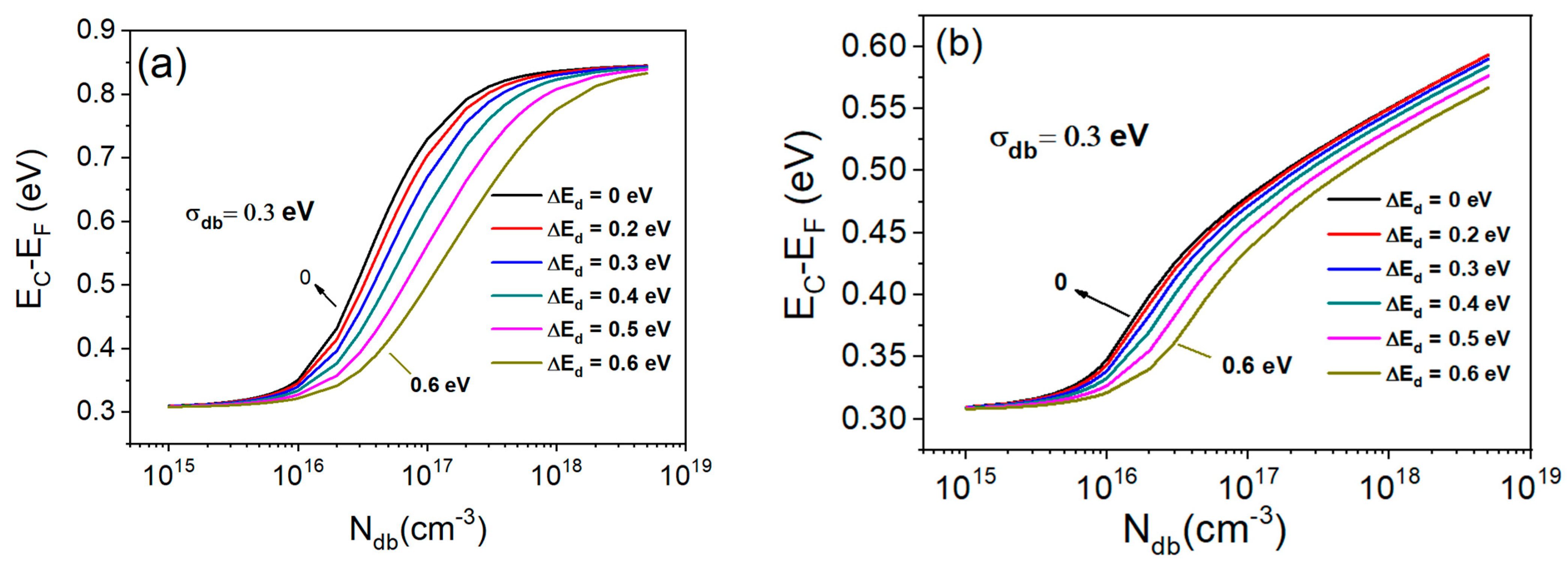
This explanation is supported by the Fermi level curve (Figure 3), which shifts toward the middle of the forbidden band either with an increase in Ndb or a decrease in the energy ΔEd. However, this dependence is less pronounced under illumination due to the photogeneration of free carriers.
Figure 3.
Fermi level position versus dangling bond density for different ΔEd: (a) dark, (b) illuminated.
4.2. Correlation Energy ΔEd Effect
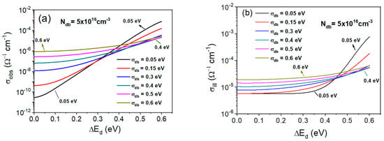
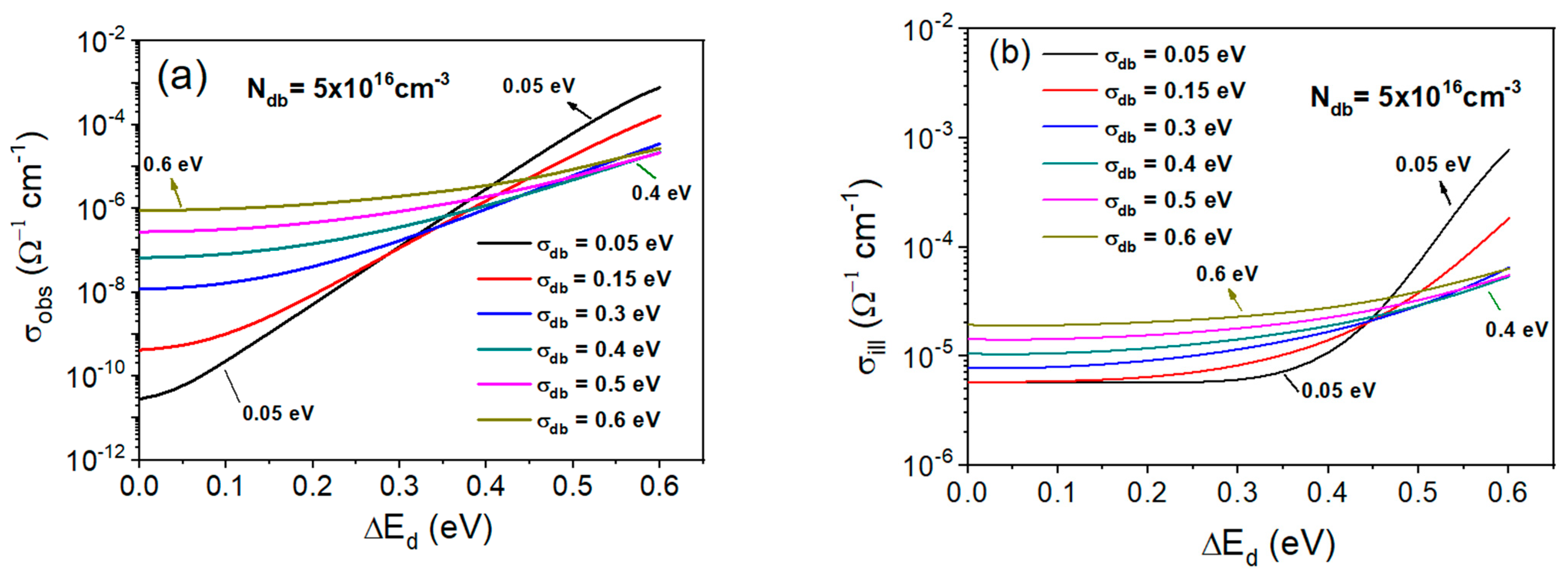
To emphasize the role of the correlation energy ΔEd, defined as the energy separation between donor and acceptor centers, Figure 4 illustrates its effect on the conductivity of a-Si:H at a fixed dangling bond concentration of 5 × 1016 cm−3. The parameter σdb is varied between 0.05 eV and 0.6 eV.
Figure 4.
Conductivity σ versus correlation energy for different standard deviations σdb: (a) dark, (b) illuminated conditions.
The correlation energy ΔEd characterizes the energetic separation between the donor-like and acceptor-like dangling bond states. Increasing ΔEd shifts these states farther away from the middle of the bandgap, thereby reducing their interaction and their effectiveness as trapping and recombination centers. Conversely, decreasing ΔEd brings the donor-like and acceptor-like distributions closer together. Although this increases their overlap, an excessive overlap also reduces their effectiveness because the distinction between the two defect-state distributions becomes less pronounced. Consequently, the electrical conductivity is governed by a complex interplay between the correlation energy and the dangling bond distribution.
The observed behavior can be explained as follows: the conductivity reaches its minimum value when the overlap between the defect-state distributions is maximal, corresponding to the smallest standard deviation σdb = 0.05 eV. In this case, the total dangling bond density Ndb reaches its highest value (see Equation (23)), leading to strong carrier trapping and consequently reduced conductivity. As the correlation energy ΔEd increases, the conductivity gradually rises because the D+ and D− states move farther away from the middle of the bandgap.
For 0 ≤ ΔEd ≤ 0.4 eV, a simultaneous increase in σdb and ΔEd results in an enhancement in conductivity. This behavior can be attributed to two combined effects:
The overlap between the dangling bond distributions NDB− (acceptor-like states) and NDB+ (donor-like states) becomes more significant as σdb increases.
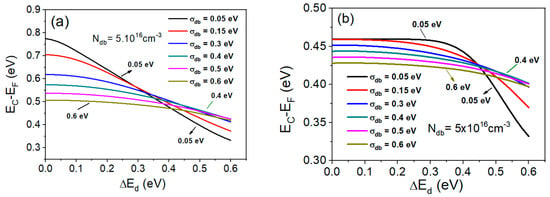
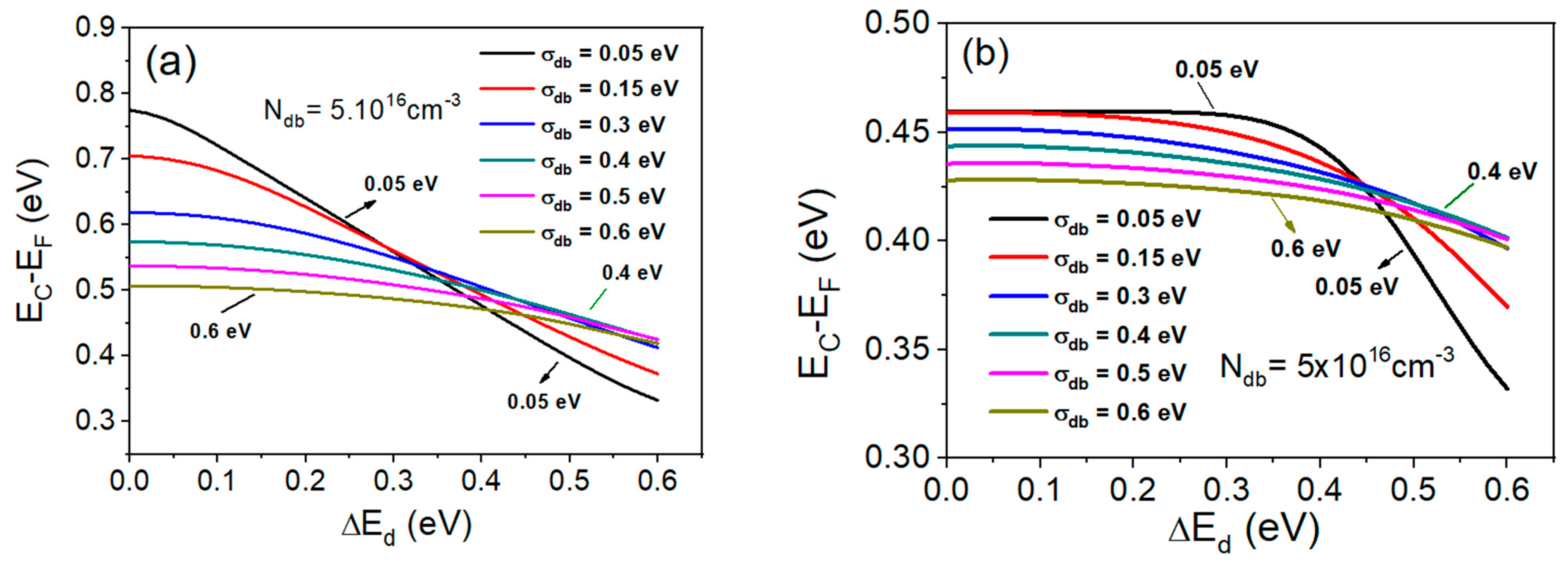
The increase in the energy separation ΔEd between the D+ and D− centers shifts these trap states away from the middle of the bandgap. As a result, the capture probability of electrons or holes by neutral D0 centers decreases, causing the Fermi level EF to move closer to the conduction band edge EC (see Figure 5).
Figure 5.
Fermi level position versus correlation energy ΔEd for different standard deviations σdb: (a) dark, (b) illuminated conditions.
For 0.5 ≤ ΔEd ≤ 0.60 eV and 0.05 ≤ σdb ≤ 0.15 eV, an opposite trend between σdb and ΔEd is observed, leading to a further increase in conductivity. This behavior reveals the complex interplay between the correlation energy ΔEd and the standard deviation σdb. Interestingly, this phenomenon appears to be specific to undoped amorphous silicon and has not been observed in doped a-Si:H layers.
4.3. Standard Deviation σdb
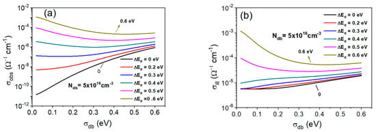
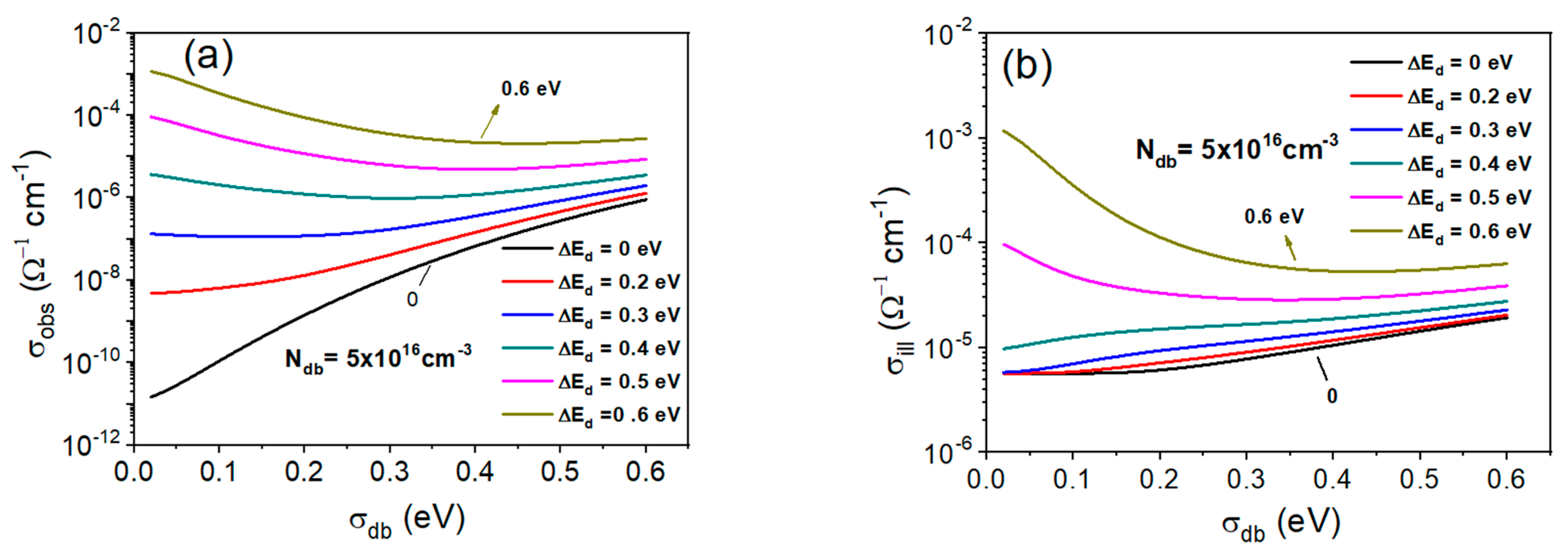
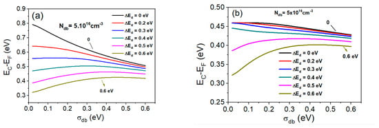
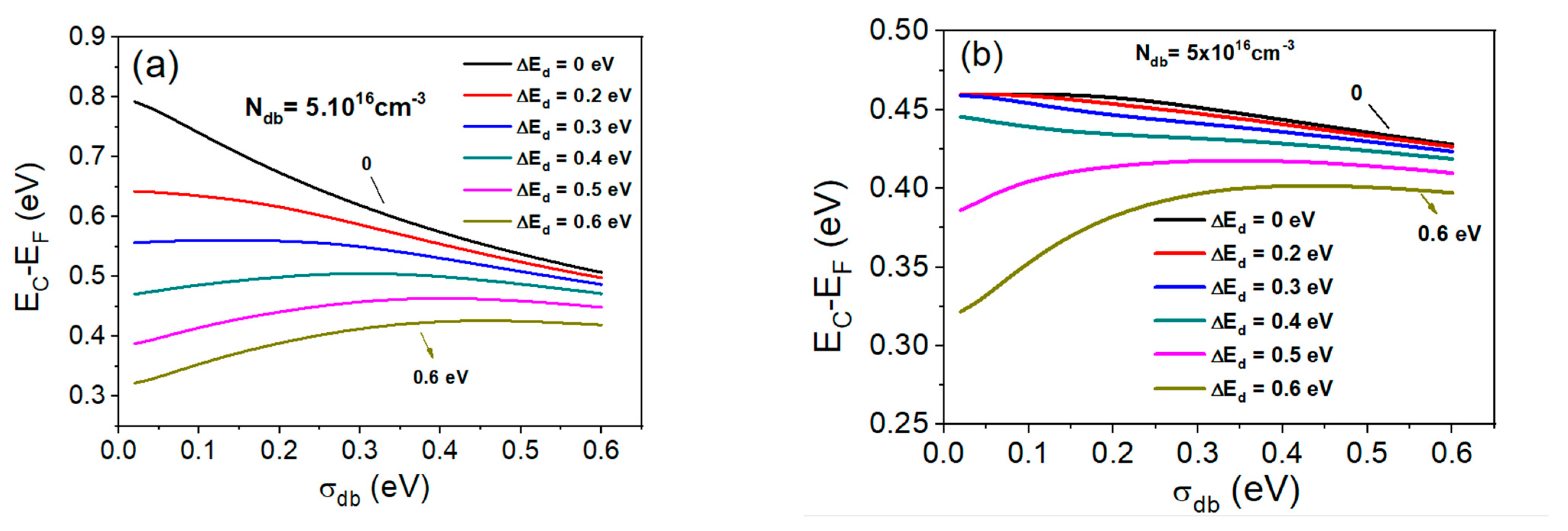
The last parameter examined is the standard deviation σdb which defines the width of the Gaussian distributions of dangling bond states. Figure 6 shows its effect for a fixed dangling bond density Ndb = 5 × 1016 cm−3 and correlation energies ΔEd ranging from 0 to 0.6 eV.
Figure 6.
Conductivity σdb versus standard deviation for different correlation energies ΔEd: (a) dark, (b) illuminated conditions.
For 0 ≤ ΔEd ≤ 0.40 eV, a simultaneous increase in σdb and ΔEd leads to an enhancement in conductivity, in agreement with the behavior observed in the previous curves.
For 0.5 ≤ ΔEd ≤ 0.60 eV and 0.05 ≤ σdb ≤ 0.3 eV, the conductivity decreases before reaching a saturation region for 0.4 ≤ σdb ≤ 0.6 eV. A similar behavior is observed for the Fermi level evolution curves (see Figure 7).
Figure 7.
Fermi level position standard versus deviation σdb for different correlation energy ΔEd: (a) dark, (b) illuminated conditions.
5. Conclusions
This work has highlighted the significant influence of dangling bond defect states on the electrical conductivity and Fermi level position of intrinsic a-Si:H under both dark and illuminated conditions. Using a self-consistent numerical solution of the semiconductor transport equations, the effects of the principal dangling bond Density-of-States (DOS) parameters, namely the dangling bond density Ndb, the correlation energy ΔEd, and the Gaussian standard deviation σdb, were systematically investigated.
The results demonstrate that the electrical conductivity of intrinsic a-Si is primarily governed by the characteristics of the dangling bond distribution. An increase in the dangling bond density significantly reduces the conductivity owing to enhanced carrier trapping and recombination through deep localized states, while variations in the correlation energy and Gaussian standard deviation modify the occupation of defect states, resulting in noticeable changes in carrier transport and Fermi level evolution under both dark and illuminated conditions. Moreover, the simulations revealed complex interactions between these parameters, particularly in intrinsic amorphous silicon, leading to behaviors that differ from those commonly observed in doped layers. Overall, this study provides a deeper understanding of the physical mechanisms associated with defect states in a-Si:H and underlines the importance of controlling dangling bond defects to improve the electrical and photovoltaic performance of amorphous silicon photovoltaic devices. Under the investigated conditions, the contribution of band-tail states was found to be negligible compared with that of dangling bonds.
Future work will extend the present model to include doped p-type and n-type a-Si layers, allowing the combined influence of band-tail states and dangling bond defects to be investigated within complete p-i-n solar-cell structures. In such devices, the interaction between localized states in the intrinsic and doped regions is expected to play an important role in carrier transport and photovoltaic performance. Furthermore, temperature-dependent simulations will be incorporated to evaluate the influence of thermal effects on carrier transport, defect-state occupation, recombination mechanisms, and electrical conductivity. Finally, comparisons with experimental measurements will be carried out to further validate the proposed physical model and assess its predictive capability for device optimization.
Author Contributions
Conceptualization, I.S. and B.Z.; methodology, I.S. and B.Z.; software, I.S.; validation, I.S., A.R. and M.A.K.; formal analysis, I.S., A.R. and A.D.; investigation, I.S.; writing—original draft preparation, I.S.; writing—review and editing, B.Z., A.R., M.A.K., Z.B., M.H. and A.D.; supervision, B.Z. and Z.B. All authors have read and agreed to the published version of the manuscript.
Funding
This research received no external funding.
Institutional Review Board Statement
Not applicable.
Informed Consent Statement
Not applicable.
Data Availability Statement
The numerical data supporting the findings of this study were generated by the simulation framework described in Section 2 and are available from the corresponding author upon request.
Acknowledgments
The authors thank their respective institutions for providing the computational environment used in this work.
Conflicts of Interest
The authors declare no conflicts of interest.
Abbreviations
The following abbreviations are used in this manuscript:
| a-Si:H | Hydrogenated amorphous silicon |
| AM1.5 | Air-mass 1.5 solar spectrum |
| BTs | Band tails |
| DBs | Dangling bonds |
| DOS | Density of States |
| PECVD | Plasma-enhanced chemical vapor deposition |
| PV | Photovoltaic |
References
- Street, R.A. Amorphous Silicon Electronics. MRS Bull. 1992, 17, 70–76. [Google Scholar] [CrossRef] [Scilit]
- Chittick, R.C.; Alexander, J.H.; Sterling, H.F. The Preparation and Properties of Amorphous Silicon. J. Electrochem. Soc. 1969, 116, 77–81. [Google Scholar] [CrossRef] [Scilit]
- Bubenov, S.S.; Vinokurov, A.A.; Yudin, I.V.; Popelensky, V.M.; Kononov, N.N.; Kuznetsova, T.A.; Dorofeev, S.G. High-Throughput Low Frequency Reactor for Non-Thermal Plasma Synthesis of Amorphous Silicon Nanoparticles. Silicon 2024, 16, 1775–1783. [Google Scholar] [CrossRef] [Scilit]
- An, S.; Choi, J.E.; Kang, J.E.; Lee, J.; Hong, S.J. Eco-Friendly Dry-Cleaning and Diagnostics of Silicon Dioxide Deposition Chamber. IEEE Trans. Semicond. Manuf. 2024, 37, 207–221. [Google Scholar] [CrossRef] [Scilit]
- Nuayi, A.W.; Ruslan, R.; Noor, F.A.; Winata, T.; Irzaman. Optical Characterization of Intrinsic Silicon Thin Films Growth via Hot Wire in Plasma-Very High-Frequency PECVD. J. Phys. Conf. Ser. 2025, 2980, 012020. [Google Scholar] [CrossRef] [Scilit]
- Brodsky, M. Plasma preparations of amorphous silicon films. Thin Solid Films 1978, 50, 57–67. [Google Scholar] [CrossRef] [Scilit]
- Mekaret, F.; Rabehi, A.; Zebentout, B.; Tizi, S.; Douara, A.; Bellucci, S.; Guermoui, M.; Benamara, Z.; El-Kenawy, E.-S.M.; Eid, M.M.; et al. A comparative study of Schottky barrier heights and charge transport mechanisms in 3C, 4H, and 6H silicon carbide polytypes. AIP Adv. 2024, 14, 115302. [Google Scholar] [CrossRef] [Scilit]
- Moustakas, T.D. Sputtered hydrogenated amorphous silicon. J. Electron. Mater. 1979, 8, 391–435. [Google Scholar] [CrossRef] [Scilit]
- Güneş, M.; Melskens, J.; Smets, A.H.M. The native and metastable defects and their joint density of states in hydrogenated amorphous silicon obtained from the improved dual beam photoconductivity method. J. Appl. Phys. 2023, 133, 125702. [Google Scholar] [CrossRef] [Scilit]
- Wang, N.; Meng, F.; Zhang, L.; Liu, Z.; Liu, W. Light soaking of hydrogenated amorphous silicon: A short review. Carbon Neutrality 2024, 3, 18. [Google Scholar] [CrossRef] [Scilit]
- Kopprio, L.; Longeaud, C.; Schmidt, J. Subgap density of states spectroscopy using steady-state photoconductivity-based experiments. J. Non-Cryst. Solids 2023, 601, 122046. [Google Scholar] [CrossRef] [Scilit]
- Luo, Y.; Flewitt, A.J. Revisiting multiple trapping and release charge transport in amorphous semiconductors exemplified by hydrogenated amorphous silicon. J. Non-Cryst. Solids 2025, 654, 123436. [Google Scholar] [CrossRef] [Scilit]
- Jeong, Y.J.; Hyun, K.J.; Jang, H.W.; Yun, J.W.; Kim, Y.H.; Park, W.I.; Choi, S.W.; Kwon, J.D. Tailoring Hydrogenation to Enhance Defect Suppression and Charge Transport in Hydrogenated Amorphous Silicon for Flexible Photodetectors. Adv. Sci. 2025, 12, e04199. [Google Scholar] [CrossRef] [Scilit] [PubMed]
- Scharfetter, D.L.; Gummel, H.K. Large-signal analysis of a silicon Read diode oscillator. IEEE Trans. Electron Devices 1969, 16, 64–77. [Google Scholar] [CrossRef] [Scilit]
- Flietner, H. U-Shaped Distributions at Semiconductor Interfaces and the Nature of the Related Defect Centres. Phys. Status Solidi (A) 1985, 91, 153–164. [Google Scholar] [CrossRef] [Scilit]
- Iftiquar, S.M.; Zilay, H. Impact of Sub Band Gap States of Amorphous Silicon Oxide Layer on Device Performance. Silicon 2024, 16, 1809–1822. [Google Scholar] [CrossRef] [Scilit]
- Solhi, A.; Sahnoune, M.; Lhermite, H.; Bonnaud, O. Numerical simulation and experimental verification of the parameters determining the base current in an a-Si: H/c-Si emitter-base heterojunction bipolar transistor. Solid-State Electron. 1992, 35, 1609–1620. [Google Scholar] [CrossRef] [Scilit]
- Gray, J. A computer model for the simulation of thin-film silicon-hydrogen alloy solar cells. IEEE Trans. Electron Devices 1989, 36, 906–912. [Google Scholar] [CrossRef] [Scilit]
- Zebentout, B.; Benamara, Z.; Mohammed-Brahim, T. Dependence of photovoltaic parameters on grain size and density of states in n+-i-p+ and p+-i-n+ polycrystalline silicon solar cells. Thin Solid Films 2007, 516, 84–90. [Google Scholar] [CrossRef] [Scilit]
- Staebler, D.L.; Wronski, C.R. Reversible conductivity changes in discharge-produced amorphous Si. Appl. Phys. Lett. 1977, 31, 292–294. [Google Scholar] [CrossRef] [Scilit]
- Sah, C.-T.; Shockley, W. Electron-Hole Recombination Statistics in Semiconductors through Flaws with Many Charge Conditions. Phys. Rev. 1958, 109, 1103–1115. [Google Scholar] [CrossRef] [Scilit]

Disclaimer/Publisher’s Note: The statements, opinions and data contained in all publications are solely those of the individual author(s) and contributor(s) and not of MDPI and/or the editor(s). MDPI and/or the editor(s) disclaim responsibility for any injury to people or property resulting from any ideas, methods, instructions or products referred to in the content. |
© 2026 by the authors. Licensee MDPI, Basel, Switzerland. This article is an open access article distributed under the terms and conditions of the Creative Commons Attribution (CC BY) license.