Abstract
Characterized by its low melting temperature of 138 °C, the eutectic Sn-58Bi solder expands the melting temperature range of interconnect joints in electronic packaging, making it widely used in multi-level packaging processes. However, its reliability at higher current densities poses a challenge. This paper employs a hybrid process combining laser soldering and hot-air reflow to fabricate Cu/Sn-58Bi/Cu solder joints in ball grid array (BGA) structures. Through mechanical testing under current loading, the effects of increasing current density (0 A/cm2, 0.85 × 10³ A/cm2, 1.70 × 10³ A/cm2, 2.55 × 10³ A/cm2, 3.40 × 10³ A/cm2, 4.25 × 10³ A/cm2) were studied systematically. Results indicate that the shear strength decreases markedly with increasing current density, exhibiting a reduction of approximately 5.63% to 95.75%. This degradation is initiated by the overall temperature increase and material softening due to Joule heating. It is further exacerbated by the loss of the non-thermal electron wind’s strengthening contribution, which weakens as the dominant thermal impact escalates with current density. Fracture mode transitions from ductile failure within the solder matrix to a ductile-brittle mixture at the solder/IMC interface, with the transition initiating at 3.40 × 10³ A/cm2. Finite element simulations reveal that current crowding in Sn-rich regions and at the solder/IMC interface induces localized Joule heating and thermomechanical strain, which jointly drive the degradation in shear strength and the shift in fracture path.
1. Introduction
Solder joints provide essential electrical and mechanical interconnections in electronic devices yet constitute their most reliability-critical elements []. The transition from 2D to 3D packaging employs vertically stacked chips or horizontal interposer distributions, utilizing solder joints with hierarchical melting temperatures to enable low-temperature assembly while minimizing thermal warpage and enhancing yield []. Low-Temperature Soldering (LTS) employs alloys such as the Sn-Bi system with a melting point below 183 °C, making it suitable for assembling heat-sensitive components and substrates. However, the inherent brittleness of its bismuth-rich phase poses challenges to mechanical reliability []. Ongoing miniaturization and higher integration densities have elevated current densities in ball grid array (BGA) joints beyond 104 A/cm2 []. Under such elevated current densities, combined with the low melting point of Sn-58Bi solder, these joints face severe reliability challenges due to current-induced degradation [,].
A major challenge for joint reliability is the current-induced accelerated failure of Sn-58Bi solder, which is driven by both thermal and non-thermal effects []. Current flow generates significant temperature increases through Joule heating, which causes softening of the solder matrix, reduced yield strength, and exacerbated thermal mismatch stresses at the interface [,,]. Microstructural heterogeneity in Sn-Bi joints leads to uneven current distribution, with localized high current density and temperature gradients in Sn-rich zones elevating electromigration risk []. Electromigration and electron wind effects drive atomic migration and microstructural evolution, including anodic Bi enrichment—whose growth correlates with Bi-rich layer thickness—increasing electrical resistance [,], while also causes phase coarsening and composition inhomogeneity [,]. It is worth noting that the microstructure formation kinetics are highly dependent on the soldering process. The laser soldering technique employed in this study effectively refines the microstructure and suppresses Bi segregation through rapid non-equilibrium solidification, yielding superior initial mechanical properties. However, under sustained current stressing, the coupled electro-thermo-mechanical fields can destabilize this metastable structure, promoting phase coarsening and interfacial voiding []. Current stressing elevates dislocation density up to 1.8 × 10¹⁷/m2 at 6.5 × 10³ A/cm2, inducing grain refinement and substructure formation that impair mechanical properties []. Non-thermal effects also promote void formation [,] and abnormal growth of IMC [,], while electromigration synergizes with isothermal aging to thicken IMC layers and increase porosity, degrading interfacial strength []. Current stress influence exhibits threshold-dependent behavior: at lower densities (1 × 10³ A/cm2 to 2 × 10³ A/cm2), non-thermal effects dominate, even causing anomalous "increase-then-decrease" strength trends []. However, once the current exceeds a critical threshold (e.g., 6 × 10³ A/cm2), the Joule heating effect intensifies dramatically and becomes the dominant mechanism []. Consequently, higher current densities relocate fracture initiation from the solder matrix to the solder/IMC interface and transition fracture mode from ductile to brittle [,,], resulting from the combined action of thermal softening, mismatch stresses, electromigration-driven void/microcrack formation, and the current crowding-induced destabilization of the interface [,,,].
Furthermore, existing research has primarily focused on traditional hot-air reflow processes, while studies on the application of other soldering techniques (such as laser soldering) in micro-joints and their reliability under current loading remain insufficient. Compared to conventional reflow soldering, laser soldering can effectively suppress IMC growth through non-equilibrium solidification, typically controlling IMC thickness below 1 μm while significantly refining the joint microstructure [,]. Notably, the formation energy of the Cu6Sn5 IMC formed by the reaction between Sn-Bi-based solder and Cu substrates is relatively high. During reflow, it often requires a longer time above the liquidus line or higher heat input to form a continuous, uniform interfacial layer []. Furthermore, parameter optimization in laser soldering yields uniformly fine β-Sn grains and a more homogeneous microstructure within the joint. The distribution of secondary IMC, like Ag3Sn further enhances material strength and hardness. These microstructural improvements lay the foundation for enhancing joint ductility and fatigue resistance [,,]. Laser soldering also mitigates the segregation tendency of Bi, promoting a more uniform distribution of eutectic structures. This reduces stress concentration points, further improving joint reliability and mechanical stability [,]. Although laser soldering demonstrates significant advantages in microstructure control and mechanical properties, current research on its reliability under realistic service conditions, such as current loading, remains insufficient. How electric current affects the evolution of mechanical properties and fracture mechanisms in laser soldering joints has not been fully elucidated.
This study employs a hybrid process combining laser soldering with hot-air reflow to fabricate Cu/Sn-58Bi/Cu solder joints. The objective is to thoroughly investigate the unique influence of current density on the shear properties and failure behavior of these joints, which exhibit excellent initial microstructures, thereby filling a gap in traditional research. The analysis examines these properties under progressively increasing current densities ranging from 0 A/cm2 to 4.25 × 10³ A/cm2. A finite element model was constructed to predict the current density and thermal profiles across the entire solder joint material. By synthesizing the simulation data, the research elucidates the underlying mechanisms through which electric current—from both thermal and non-thermal perspectives—governs the degradation in shear performance and the evolution of fracture behavior.
2. Materials and Methods
2.1. Experimental Methods
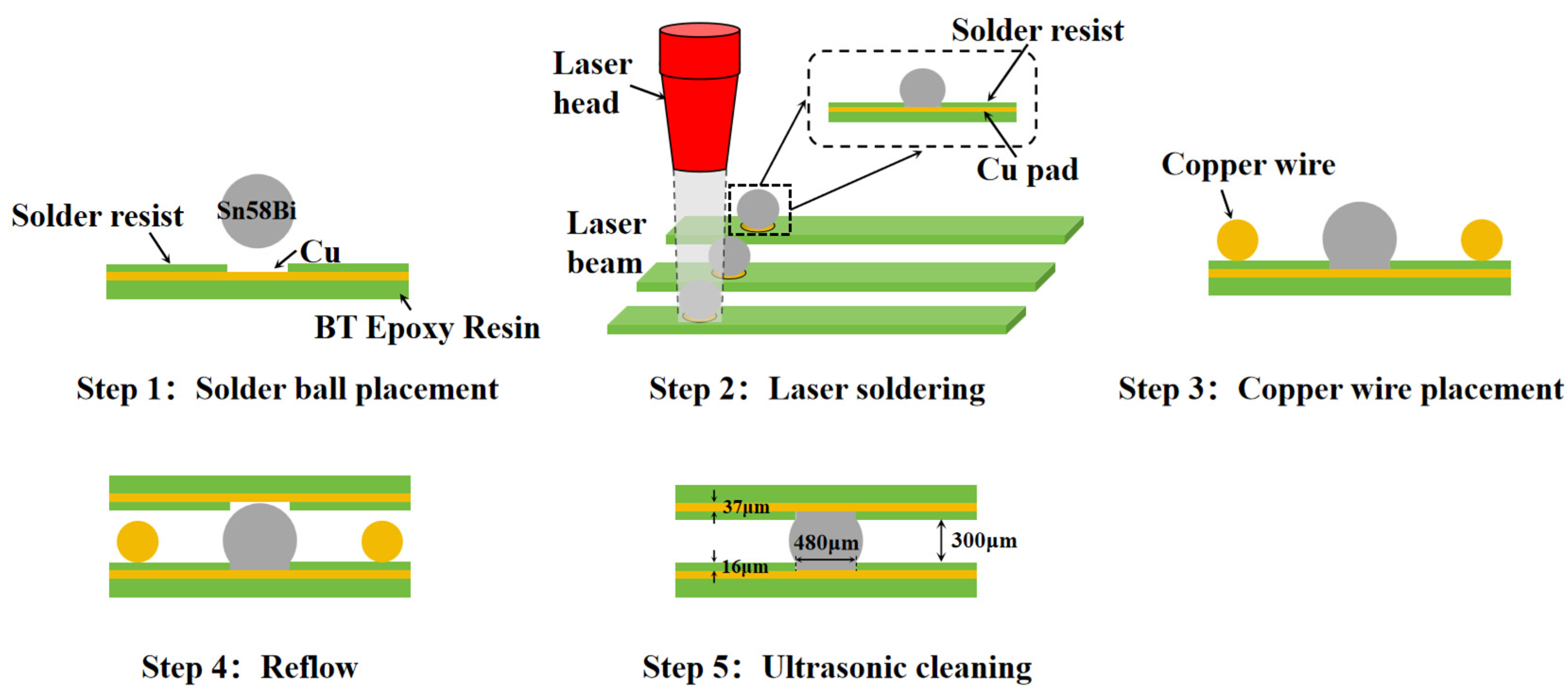
A hybrid fabrication process integrating laser soldering with hot-air reflow was utilized to produce Cu/Sn-58Bi/Cu solder joints in a BGA configuration, enabling an investigation into the effects of current density on their shear performance and fracture modes. The effects of current stress on joint performance were systematically examined through mechanical testing under current loading. The test specimens consisted of Cu/Sn-58Bi/Cu joints, which were designed with a pad diameter (d) of 480 μm and a joint height (h) of 300 μm. For this purpose, 600 μm Sn-58Bi solder balls were employed. The substrate was a solder mask defined (SMD), surface copper-clad bismaleimide triazine (BT) epoxy resin, with its surfaces pre-treated with a Cu-OSP finish. The primary laser soldering parameters considered were laser power and laser exposure time. Based on an evaluation of soldering strength and error metrics, single-interface joints produced using 25 W laser power and a 0.3 s exposure time were selected for subsequent experiments following a rigorous screening process (see Supplementary File, Figure S1).
The solder joint preparation process is as follows (as shown in Figure 1): (1) Place Sn-58Bi solder balls onto the substrate using a lead-free, halogen-free, no-clean flux. Perform laser soldering under a constant-temperature precision laser soldering machine (Anewbest, Shenzhen, China) to form single-interface solder joints. During laser soldering, the laser power was set to 25 W, and the irradiation duration was 0.3 s. (2) Assemble the single-interface solder joint with another substrate using a specialized mold. A standoff height of 300 μm for the solder joints was set by employing copper wire with a matching diameter. A peak temperature of 230 °C, sustained for 50 s, was employed during the subsequent reflow stage. Lead-free, halogen-free, no-clean flux was also used throughout the reflow process.
Figure 1.
Fabrication flowchart of Cu/Sn-58Bi/Cu solder joints.
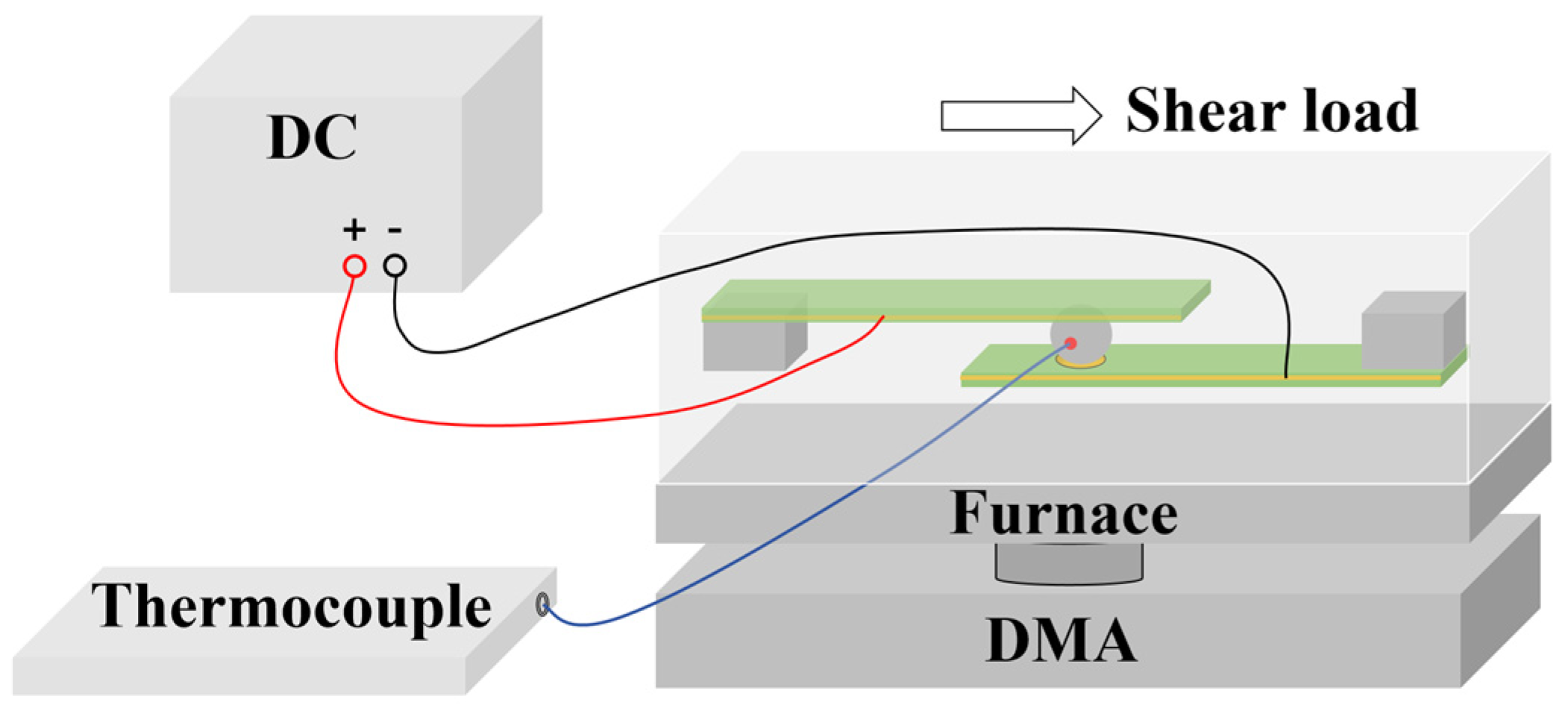
To apply a load under current, this study employed a dynamic mechanical analyzer (DMA, Q800) (TA Instuments, New Castle, DE, USA) for shear testing (see Figure 2), with a constant DC voltage and constant current power supply (KRT-3010). The fixture span was maintained at 18.0 mm, and all tests were conducted at 25.0 °C. Samples were secured in an electrically insulated fixture, followed by furnace closure and current application after thermal stabilization. Current densities ranging from 0 to 4.25 × 10³ A/cm2 were applied for 3 minutes to establish thermal equilibrium before initiating shear loading at 1.0 N/min. Data acquisition continued until specimen failure.
Figure 2.
Illustration of the shear test configuration for BGA solder joints subjected to electrical current.
After the sample fracture, the fracture morphology of the solder joint was characterized using a scanning electron microscope (SEM, TESCAN MIRA LMS) (TESCAN, Brno, Czech Republic) equipped with an energy-dispersive spectrometer (EDS, Oxford Xplore 30) (Oxford Instruments, Oxford, UK) and a laser confocal microscope (OLS4100) (Olympus, Tokyo, Japan). Additionally, the KIC X5-9 thermocouple was employed to monitor the surface temperature of the solder joints in real time. The test conditions were conducted at room temperature (25 °C) with an energization duration of 300 s.
2.2. Finite Element Methods
Finite element simulations were conducted using COMSOL Multiphysics 6.2 to investigate how current density affects the shear performance and fracture behavior of Cu/Sn-58Bi/Cu solder joints. Figure 3 presents the joint microstructure and corresponding simulation model. Figure 3a displays the typical microstructural morphology of solder joints fabricated via the hybrid process. It can be observed that the eutectic Sn-58Bi structure consists of dark Sn-rich phases interwoven with bright Bi-rich phases, forming a characteristic eutectic morphology combining lamellar and granular phases. However, due to the rapid solidification nature of laser soldering, the microstructure exhibits significant refinement, with smaller and more uniform phase sizes. Based on this actual microstructure, a geometric model for finite element simulation was constructed, as shown in Figure 3b. We employed COMSOL 6.2 software to convert two-dimensional microstructure images of solder joints into geometric entities using the nearest-neighbor interpolation method. This approach simplified regions smaller than 2 μm2 while preserving the actual arrangement of Sn/Bi phases. The primary meshing strategy utilized a three-node free triangular mesh. Considering the small microstructural scale of Sn and Bi phases, local mesh refinement was applied to these regions during meshing to ensure computational accuracy. The mesh across all domains in the model comprised 3,748,490 elements, with a minimum element size of 0.243 μm and a maximum element size of 54.3 μm. The average mesh quality was 0.8214. By systematically refining the mesh, two key output variables—maximum solder joint temperature and maximum current density—were monitored. Boundary conditions included: constant current density applied to one Cu pad with the opposite side grounded; convective cooling on external surfaces; and constrained normal displacement at Cu pad surfaces to prevent rigid body motion. Mesh independence was verified through systematic refinement, monitoring maximum temperature and current density until convergence was achieved.
Figure 3.
(a) The microstructure of Cu/Sn-58Bi/Cu solder joint; (b) finite element simulation model.
The finite element model was employed to analyze temperature distribution and quantify current density in Sn/Bi phases under various operating conditions. A coupled multiphysics framework was established to simulate electromechanical response and damage evolution. Material properties for Sn, Bi, and Cu incorporated temperature-dependent functions directly from the COMSOL Multiphysics 6.2 material library to ensure simulation accuracy. Specific parameters are detailed in Table 1.
Table 1.
Material properties used in the simulation.
3. Results
3.1. Deformation of Solder Joints Under Current Loading
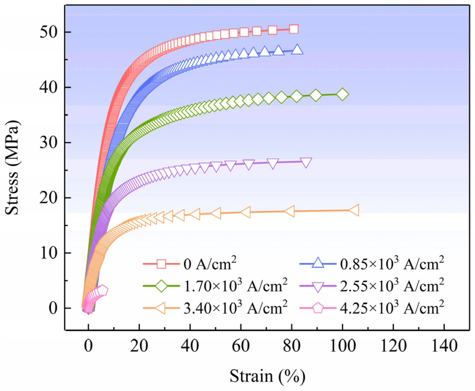
Following the fabrication process, the shear properties of the solder joints were characterized using DMA to obtain stress-strain responses at different current densities (see Figure 4). These electro-mechanical characteristics demonstrate current density’s significant influence on deformation behavior. Below 3.40 × 10³ A/cm2, the curves displayed two distinct regimes: initial linear elastic deformation followed by nonlinear accelerated deformation. The elastic stage showed rapid stress increase with strain, while the subsequent stage exhibited dramatic strain accumulation with minimal stress variation. At zero current density, joints demonstrated high initial modulus and extensive plastic deformation, achieving maximum shear strength. With current increased to 0.85 × 10³ A/cm2, similar characteristics persisted though with marginally reduced stress levels, indicating initial current influence. At 3.40 × 10³ A/cm2, enhanced nonlinearity emerged alongside reduced initial stress and nearly diminished strain hardening. A fundamental transition occurred at 4.25 × 10³ A/cm2, where deformation became predominantly linear with essentially eliminated plastic flow capacity.
Figure 4.
The stress-strain curves of Cu/Sn-58Bi/Cu solder joints at different current densities.
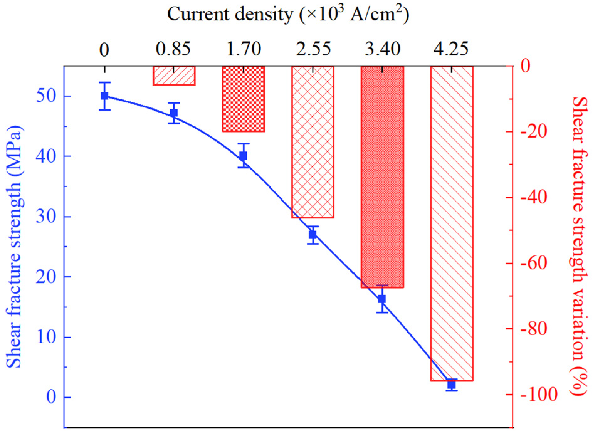
The mean shear strength, derived from experimental stress-strain curves, demonstrates a clear dependence on current density as summarized in Figure 5. A progressive decrease in shear strength is observed across the current density range from 0 to 4.25 × 10³ A/cm2, confirming that electrical stress significantly compromises mechanical integrity, with pronounced degradation under high current conditions []. This accelerated deterioration results from the coupled electro-mechanical stresses that jointly exacerbate property degradation in solder joints.
Figure 5.
Shear fracture strength variation in Cu/Sn-58Bi/Cu solder joints at different current densities.
An assessment of current-induced deterioration was conducted through comparative analysis of shear fracture strength with and without electrical loading across different current densities. The results are shown in Figure 5. A similar trend was observed between the shear strength and its variation rate. Specifically, the variation rate exhibited a pronounced reduction from −5.63% to −95.75% with increasing current density over the range of 0.85 × 10³ A/cm2 to 4.25 × 10³ A/cm2.
3.2. Fracture Behavior of Solder Joints Under Current Loading
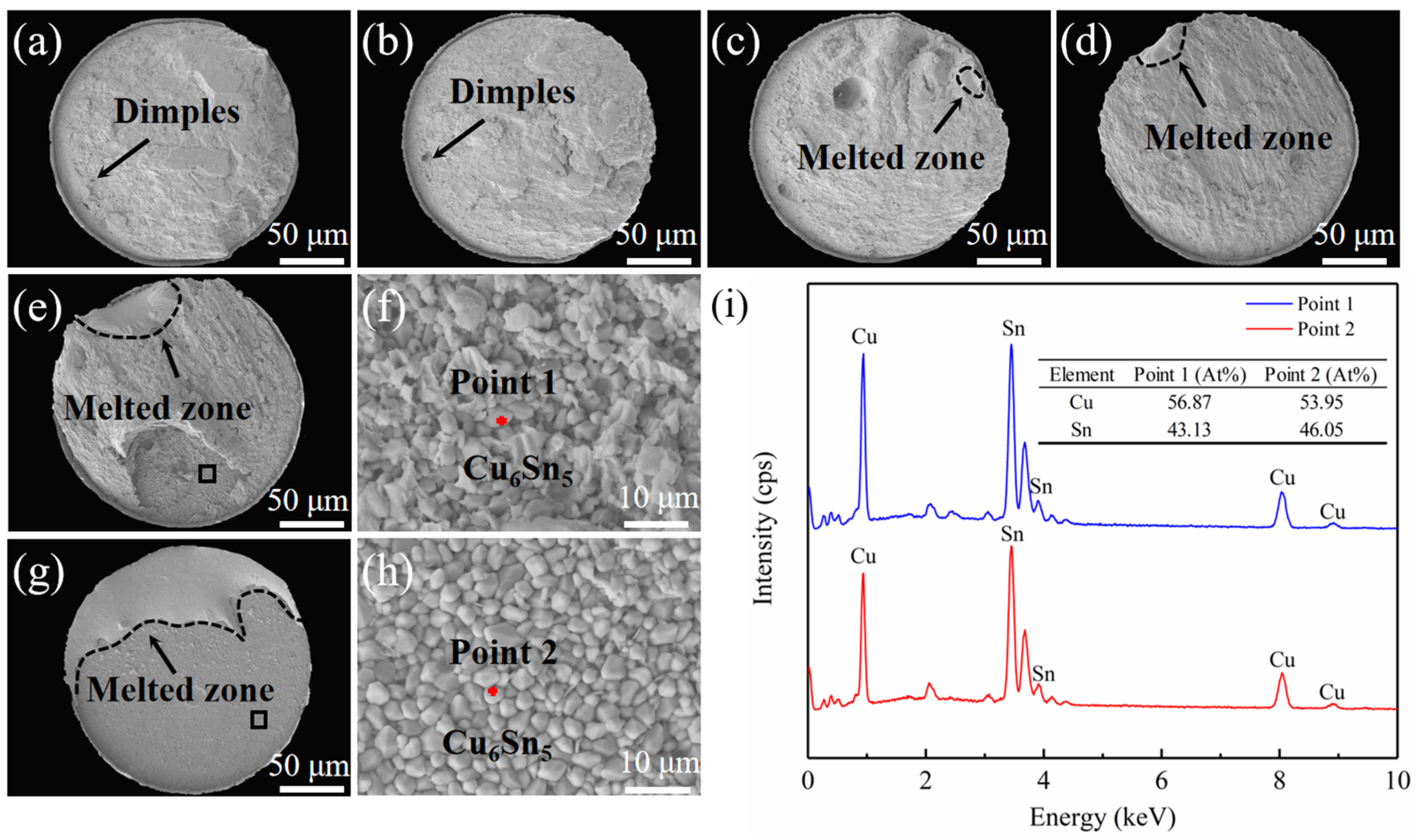
The shear fracture morphology of Cu/Sn-58Bi/Cu solder joints under current loading is shown in Figure 6. At a current density of 0 A/cm2, fracture occurs within the solder matrix, exhibiting ductile pitting on the fracture surface and characteristic ductile fracture behavior [], as depicted in Figure 6a. The ductile nature of the fracture morphology was preserved even at the current density of 1.70 × 10³ A/cm2. However, localized solder melting began to appear at the fracture edges, indicating that temperatures in these areas approached the solder melting point, as shown in Figure 6c. This localized melting intensified with increasing current density, further influencing the fracture behavior of the joints. At 3.40 × 10³ A/cm2, distinct granular regions became visible on the fracture surface, as shown in Figure 6e. EDS analysis confirmed that these particles observed on the fracture surface were Cu6Sn5 IMC (see Figure 6i), indicating interfacial fracture at this current density with mixed ductile-brittle fracture characteristics. At a current density of 4.25 × 10³ A/cm2, the proportion of interfacial fracture further increased, with more pronounced brittle fracture characteristics [], as shown in Figure 6g. The interfacial fracture area was significantly larger than the molten region at this stage, demonstrating the predominance of brittle interfacial fracture over the diminishing ductile characteristics of the solder matrix. This observation signifies a shift in the joint’s failure mechanism, progressing from ductile fracture to a predominantly brittle mode with mixed characteristics.
Figure 6.
Fracture morphologies of Cu/Sn-58Bi/Cu solder joints at different current densities: (a) 0 A/cm2; (b) 0.85 × 10³ A/cm2; (c) 1.70 × 10³ A/cm2; (d) 2.55 × 10³ A/cm2; (e) 3.40 × 10³ A/cm2; (f) partially enlarged view of the rectangular area in (e); (g) 4.25 × 10³ A/cm2; (h) partially enlarged view of the rectangular area in (g); (i) EDS results for points 1 and 2.
To further examine the fracture mechanism of the solder joints, cross-sectional observations of the fracture surfaces were conducted, with results shown in Figure 7. In the absence of electrical current, the fracture occurred at a distance from the Cu pad that was consistent with the thickness of the solder mask, as shown in Figure 7a. Upon increasing the current density to 2.55 × 10³ A/cm2, the fracture characteristics resembled those observed without current application, with no exposed IMC visible (Figure 6d). This indicates that a fracture still occurred within the solder matrix at this current density, as shown in the cross-section of Figure 7d. As the current density was elevated to 3.40 × 10³ A/cm2, combining the characterization results from Figure 6e and Figure 7e, a small portion of IMC grains was found to be present on the fracture surface, indicating partial interfacial fracture of the solder joint at this current density. With the current density rising to 4.25 × 10³ A/cm2, the Cu layer surface in the fracture was primarily composed of IMC grains with a minor amount of solder. The exposed IMC surface is explained by interfacial fracture, with the scant solder residue accounted for by subsequent melting and coating of the interface. The results demonstrate that the fracture behavior of Cu/Sn-58Bi/Cu joints exhibits significant current density dependence under current loading []. A progressive evolution in fracture mode occurred with increasing current density, manifested as a transition from ductile fracture within the solder to a mixed ductile-brittle failure at the solder/IMC interface, in agreement with the stress-strain curve findings (see Figure 4).
Figure 7.
Cross-sectional morphology of fatigue fracture in Cu/Sn-58Bi/Cu solder joints under current loading (Interfacial region near substrate): (a) j = 0 A/cm2; (b) j = 0.85 × 10³ A/cm2; (c) j = 1.70 × 10³ A/cm2; (d) j = 2.55 × 10³ A/cm2; (e) j = 3.40 × 10³ A/cm2; (f) j = 4.25 × 10³ A/cm2.
4. Discussion
4.1. Mechanism of Degradation in Shear Performance of Solder Joints Under Current Loading
4.1.1. Overall Temperature Rise Caused by Joule Heating Effect and Material Softening
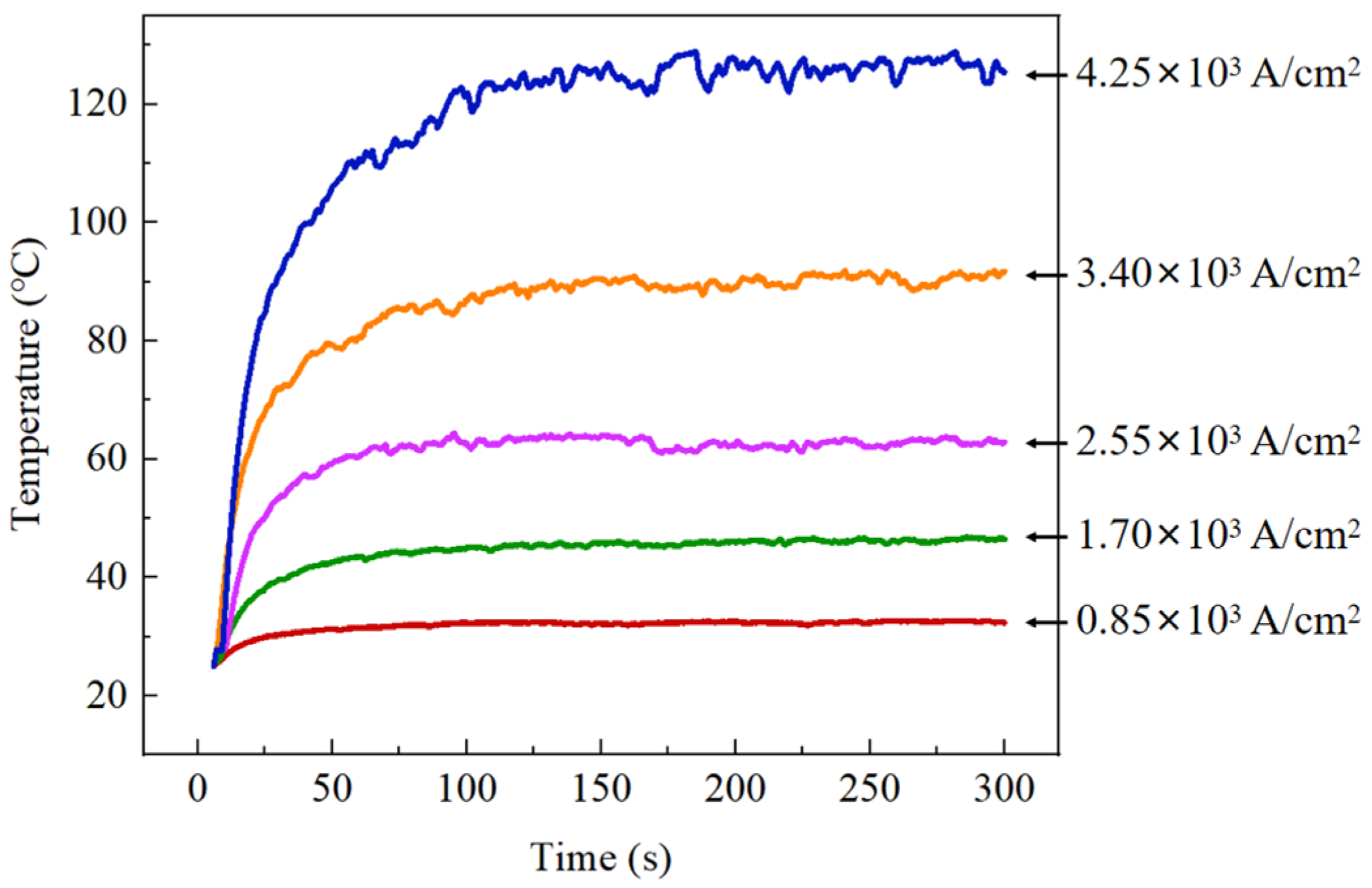
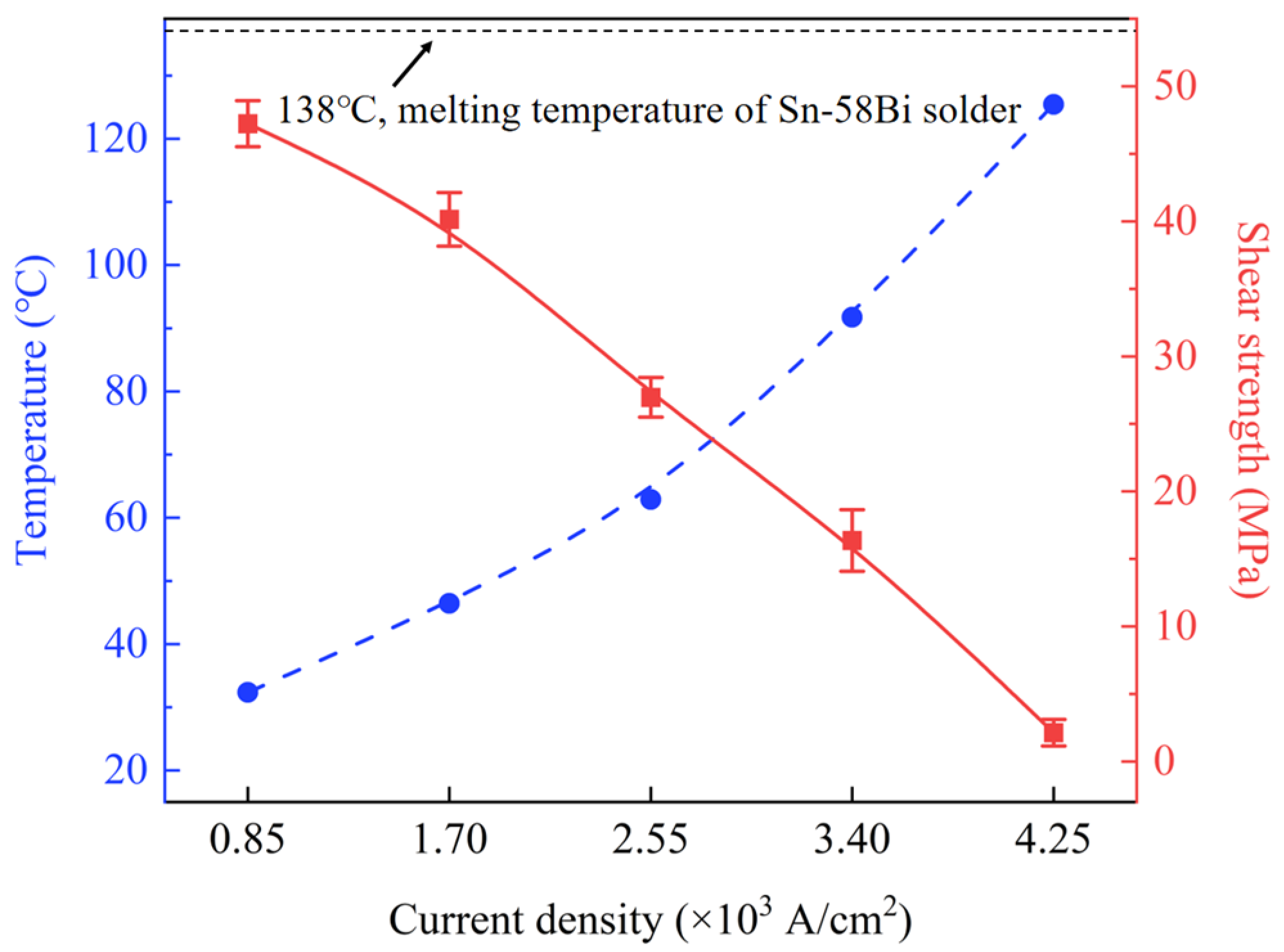
To investigate the mechanism by which the Joule heating effect influences the mechanical shear response of Cu/Sn-58Bi/Cu solder joints, this study systematically measured temperature changes within the solder joints subjected to varying current densities. The effect of Joule heating on the microstructural development and mechanical properties of the solder joint was investigated through combined finite element simulations and experimental analysis. Experimental results indicate that under current densities of 0.85 × 10³ A/cm2, 1.70 × 10³ A/cm2, 2.55 × 10³ A/cm2, 3.40 × 10³ A/cm2, and 4.25 × 10³ A/cm2, the solder joints’ temperature continuously increased within 100 s of current application before gradually stabilizing to reach a steady-state thermal equilibrium. Figure 8 displays the temperature-versus-time curves for solder joints under different current densities. It can be observed that as the current density increases, the steady-state temperature of the solder joint rises from 30 °C to over 120 °C, approaching the melting point of Sn-58Bi (138 °C). When the current density reaches 0.85 × 10³ A/cm2, the solder joint temperature increases by approximately 5 °C within 100 s, ultimately stabilizing around 30 °C. Conversely, upon reaching a current density of 4.25 × 10³ A/cm2, the solder joint temperature rose by approximately 95 °C within 100 s, eventually stabilizing above 120 °C. The increase in temperature of the solder joint correlates positively with the current density, as depicted in Figure 9. According to Joule’s law, the heat dissipation QJoule can be expressed as []:
where I represents the current flowing through the solder joint; RS denotes the electrical resistance of the solder material; t is the duration of current application; AS is the cross-sectional area of the solder joint; j is the current density within the solder joint; is the resistivity of the solder; h is the height of the solder joint. Increasing current density directly enhances Joule heating within solder joints, resulting in proportionally higher temperature rise. Experimental observations confirm that Joule heating governs the thermal response of solder joints under elevated current density conditions.
Figure 8.
Temperature as a function of time for solder joints exposed to different current densities.
Figure 9.
Variation of solder joints shear strength with temperature at different current densities.
The actual temperature of the solder joints under current loading is significantly elevated above the ambient test temperature due to the Joule heating effect. The operational temperature within the solder joint can be quantified using the following formula []:
where ht denotes the convective coefficient; S is the surface area for heat transfer; C represents the solder’s specific heat capacity; m0 is the mass of the solder matrix material; Ta is the ambient temperature.
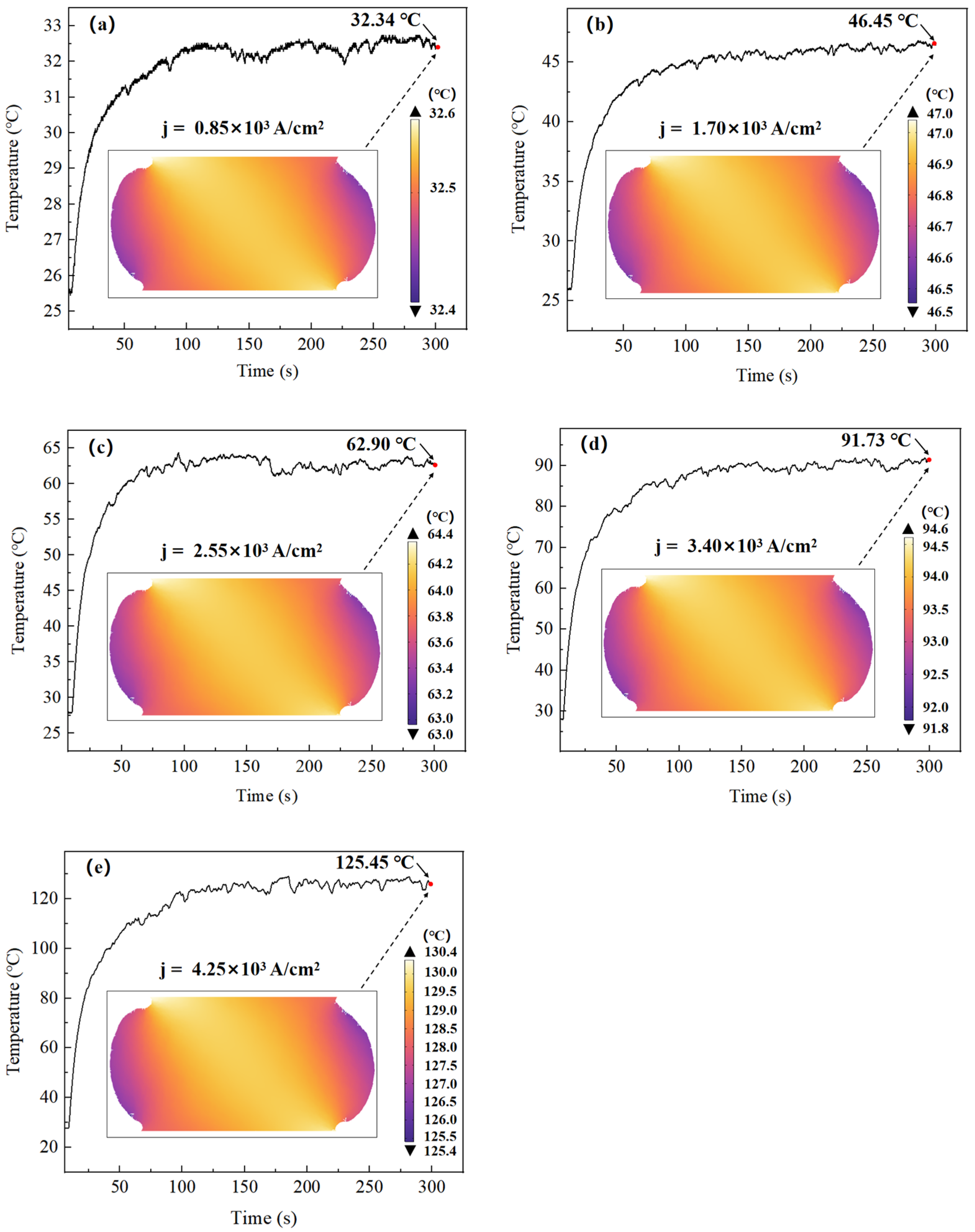
To elucidate the mechanism through which Joule heating influences joint shear performance, this research employed the finite element method to simulate actual temperature distributions based on the aforementioned formula. The simulation results shown in Figure 10 reveal a relatively uniform temperature distribution within the solder joint. The simulated temperatures show strong agreement with experimentally obtained values, indicating that the measured temperature during testing can be attributed primarily to Joule heating effects. Given that the temperature increase caused by Joule heating reflects the Joule heating effect within the solder joint, the measured temperatures show that this effect is more significant under high current density conditions []. Under conditions of current density at 0.85 × 10³ A/cm2 (see Figure 10a), the Joule heating-induced temperature within the joint (32.6 °C) was only 7.6 °C higher than the measured temperature (25 °C). However, at a current density of 4.25 × 10³ A/cm2, the Joule heating-induced temperature within the solder joint reached 130.4 °C (see Figure 10e), far exceeding the test temperature. This also demonstrates that the finite element model accurately reflects the thermal distribution within the solder joint under varying current densities. This temperature distribution suggests that the temperature increase due to the Joule heating effect is widespread throughout the solder joint.
Figure 10.
Simulated temperature distribution in Cu/Sn-58Bi/Cu solder joints at different current densities: (a) j = 0.85 × 10³ A/cm2; (b) j = 1.70 × 10³ A/cm2; (c) j = 2.55 × 10³ A/cm2; (d) j = 3.40 × 10³ A/cm2; (e) j = 4.25 × 10³ A/cm2.
The thermal softening induced by increasing joint temperatures was identified as the primary cause of the marked deterioration in shear strength, as shown in Figure 9. Moreover, as current density increases, the solder joint temperature gradually rises from its initial room temperature (approximately 25 °C). Upon reaching a current density of 4.25 × 10³ A/cm2, the solder joint temperature approaches the melting point of Sn-58Bi. This temperature increase, driven by the Joule heating effect, results in thermal softening of the solder matrix. As a result, the solder exhibits a considerable decrease in both yield strength and shear resistance at elevated temperatures [], becoming the primary cause of strength degradation in the high-current range.
Differences in the CTE between materials also significantly influence the mechanical shear resistance of the solder joint. Due to the distinct CTE values of Sn-58Bi solder, copper, and IMC, these materials expand at different rates when temperatures rise due to Joule heating, resulting in thermal expansion mismatch. This mismatch generates substantial thermal stresses that further weaken the bond strength at the interface.
4.1.2. Non-Thermal Strengthening Mechanism of Electron Wind in Low-Current Range
While Joule heating dominates shear strength degradation at high current densities, the more gradual decline observed at lower current levels (0~1.70 × 10³ A/cm2) (as shown in Figure 5) suggests competing non-thermal mechanisms prior to the onset of dominant thermal softening. The principal non-thermal influence is the electron wind force, which arises from momentum transfer between drifting electrons and the atomic lattice. This force promotes dislocation motion and proliferation, thereby affecting the mechanical properties of the solder joint []. The term “electron wind force” () refers to the force exerted by flowing electrons on atomic lattices. It is quantified by the equation []:
Here, Z* stands for the effective charge, e represents the electron charge, is the resistivity of the solder, and j is the current density. The intensified electron wind at elevated current densities promotes dislocation multiplication, which contributes to a strengthening effect in solder joints under low-current conditions. In line with the Taylor relation, the correlation between lattice stress () and dislocation density (d) can be formulated as []:
Here, , G, b, and d correspond to the dislocation interaction constant, the shear modulus, the Burgers vector, and the dislocation density, respectively. An increase in dislocation density leads to heightened lattice stress. This implies that in regions of low current density and low temperature, non-thermal effects may exert a slight strengthening influence on the solder joint, partially offsetting the initial, weaker Joule heating softening effect.
On the other hand, current also induces significant lattice diffusion behavior. Under the combined action of the electric field and electron wind, atoms (or vacancies) undergo directional migration along specific orientations. The current-driven lattice atomic diffusion flux (J) can be expressed as []:
Here, D represents the diffusion coefficient, n is the atom concentration within the lattice during diffusion, kB denotes the Boltzmann constant, and t is the external temperature. Under low current conditions, this process can induce local compositional fluctuations, thereby altering phase boundary structures and defect distributions, exerting additional effects on the material deformation mechanism.
At low current densities, the synergistic action of non-thermal mechanisms induces moderate dislocation multiplication and microstructural refinement, thereby providing limited strengthening to the joint. However, this enhancement diminishes with increasing current density due to intensified dynamic recovery processes that counteract dislocation proliferation []. Simultaneously, the rapidly escalating Joule heating effect induces substantial temperature rise, whose dominant thermal softening effect eventually overwhelms the non-thermal contributions. When the current density exceeds 1.70 × 10³ A/cm2, Joule heating becomes the governing factor determining joint strength. Furthermore, the electron wind force modifies internal stress distribution through its influence on dislocation dynamics: while promoting organized dislocation motion at low current densities, intensified electron wind at higher levels induces disordered dislocation movement that accelerates recovery processes and contributes to mechanical degradation.
The competing interplay between thermal and non-thermal effects governs the current-dependent shear strength evolution: non-thermal strengthening predominates in the low-current regime, whereas Joule heating-induced thermal degradation becomes governing at elevated current densities, ultimately leading to substantial mechanical deterioration.
4.2. Evolution Mechanism of Fracture Behavior in Solder Joints Under Current Loading
4.2.1. Interface Strain Mismatch and Fracture Mechanism Transition
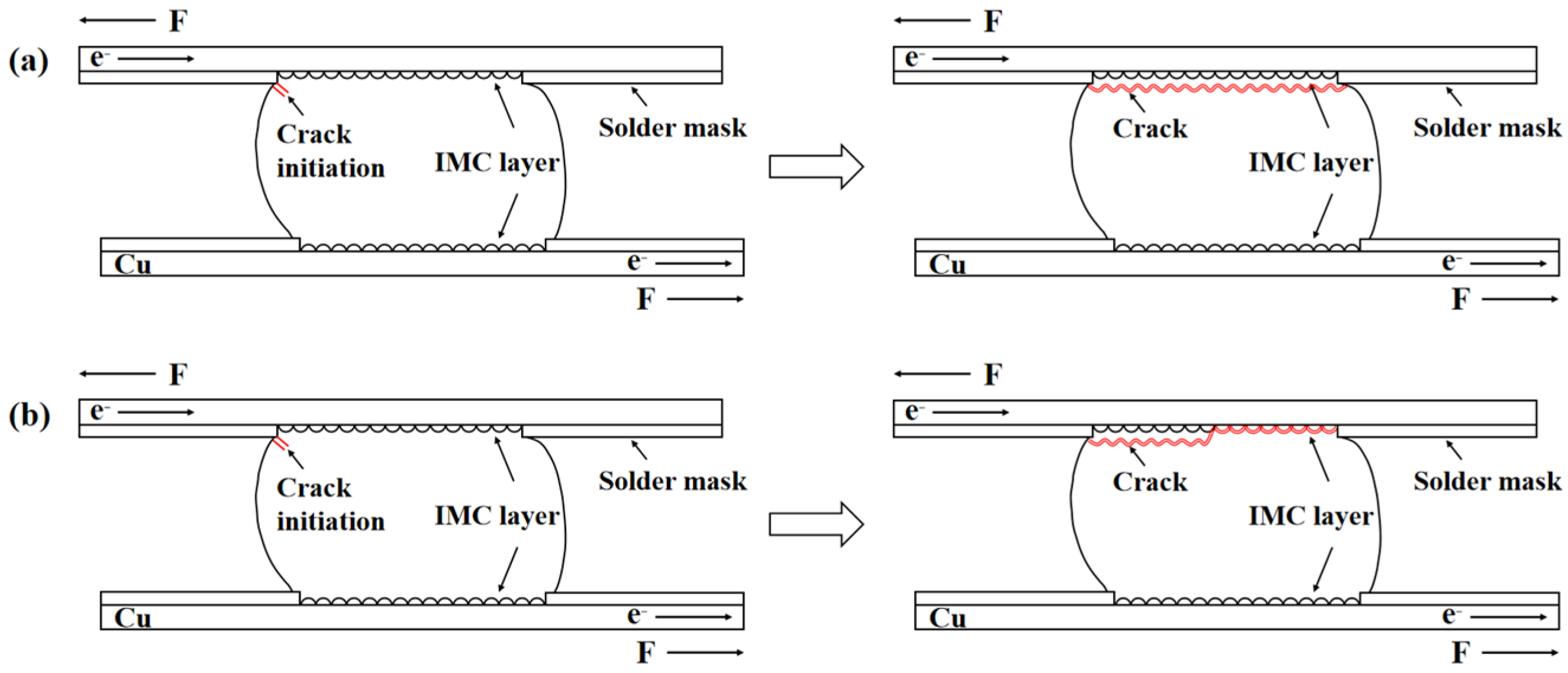
Electric current significantly influences the fracture mechanisms of Cu/Sn-58Bi/Cu solder joints, with its effects particularly evident in the transition of fracture modes and evolution of failure mechanisms. As shown in the experimental results above, with increasing current density from 0 A/cm2 to 4.25 × 10³ A/cm2, the fracture mode of the solder joint primarily evolves into two distinct types (as depicted in Figure 11). This figure clearly illustrates how, as current density increases, the fracture path gradually migrates from the interior of the solder matrix—which possesses the highest stress-bearing capacity (Figure 11a)—to the solder/IMC interface, where current concentration, Joule heating, and strain mismatch exert the most severe effects (Figure 11b). The evolution shown in Figure 11 is highly consistent with the stress-strain curve characteristics (gradual loss of plastic deformation capacity) in Figure 4 and the cross-sectional morphology observations in Figure 6 and Figure 7. This demonstrates that the transition in fracture mode is an inevitable outcome of the coupled thermal-electrical-mechanical multiphysics effects under electrical stress. The fracture mode transitions from ductile failure within the solder matrix to predominantly brittle fracture along the solder/IMC interface. While Bi addition refines the Sn-based microstructure and enhances fracture toughness [], elevated current density counteracts this beneficial effect and promotes brittle failure. This transition is further intensified by localized Joule heating at the interface (as shown in Figure 10), which induces thermal softening and degrades interfacial bonding. Additionally, the coefficient of thermal expansion mismatch between the solder, IMC, and Cu substrate generates substantial thermomechanical stresses during current-induced heating. These concentrated stresses accelerate interfacial crack initiation and propagation, ultimately leading to premature joint fracture.
Figure 11.
Schematic diagram of fracture locations in Cu/Sn-58Bi/Cu solder joints under current stressing: (a) fracture occurs in solder matrix; (b) fracture occurs at solder/IMC interface.
The synergistic effect of high temperature and high stress at the interface under high current density significantly promotes the formation and propagation of interfacial cracks. In previous studies on Cu/SAC305/Cu joint under tensile stress, elevated temperatures exacerbated strain mismatch at the solder/IMC layer interface, causing fracture locations to migrate from the solder matrix toward the solder joint/IMC layer interface []. Under shear stress, strain mismatch in Cu/Sn-58Bi/Cu solder joint also intensifies with increasing temperature. Furthermore, strain localization and stress redistribution further drive the fracture toward the interface. Figure 12 illustrates the distribution of equivalent strain within the solder joint, revealing that the most severe strain mismatch under current loading takes place at the solder/IMC interface, which is the driving force for interfacial fracture []. Results indicate that the intensification of strain localization and interfacial embrittlement with rising current density drives the transition in failure mechanism from bulk ductile fracture to interfacial-dominated brittle failure.
Figure 12.
Distribution of equivalent strain in Cu/Sn-58Bi/Cu solder joints at different current densities: (a) j = 0.85 × 10³ A/cm2; (b) j = 1.70 × 10³ A/cm2; (c) j = 2.55 × 10³ A/cm2; (d) j = 3.40 × 10³ A/cm2; (e) j = 4.25 × 10³ A/cm2.
4.2.2. Microcurrent Concentration and Local Property Evolution
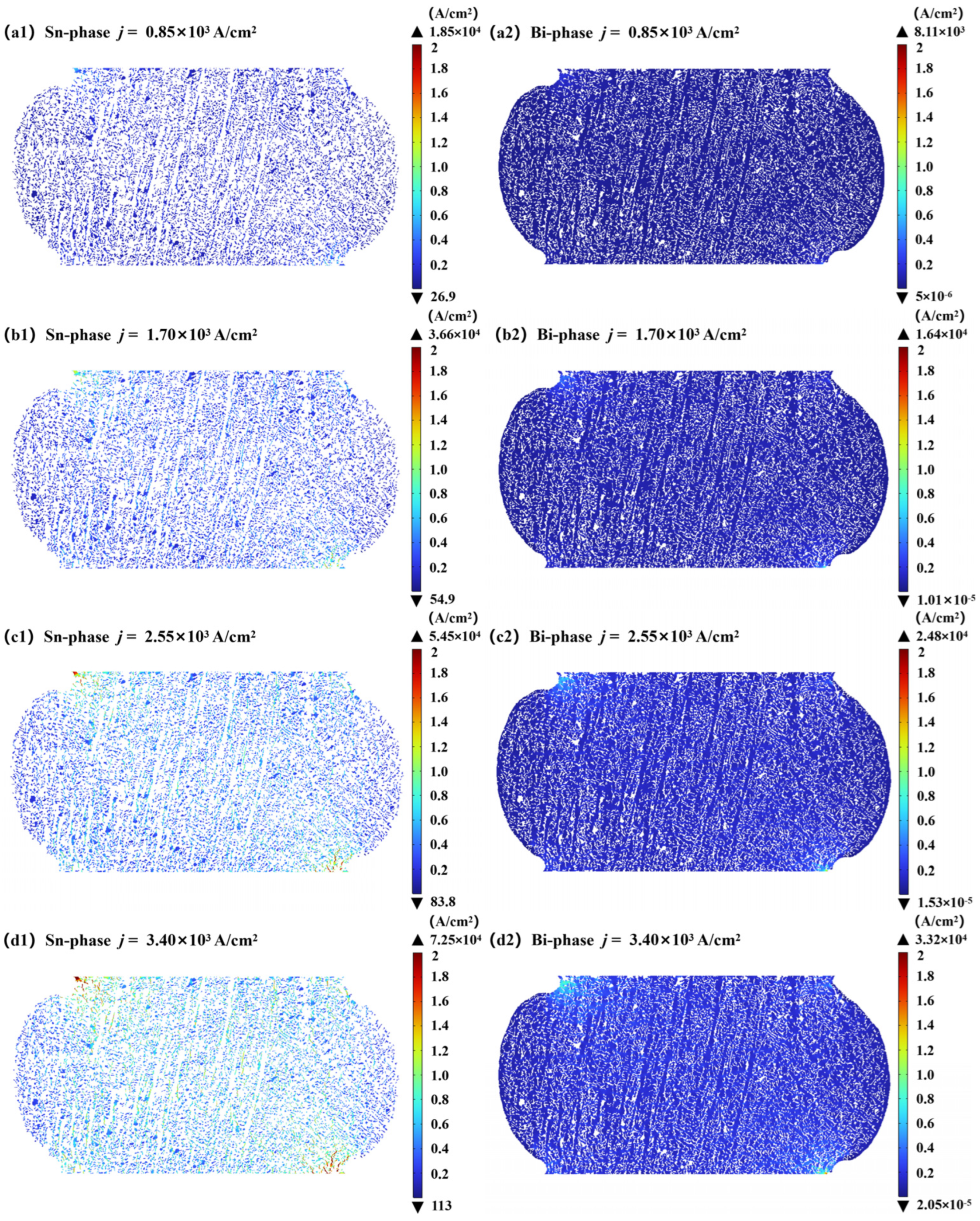
To elucidate the microscale influence of current density, we investigate its fundamental role in dictating the shear performance and fracture mechanisms of solder joints. This study employed finite element simulation based on the microstructure of the micro-solder joint depicted in Figure 3. The simulation examined the current density distribution in the Sn-rich and Bi-rich phases within the solder matrix of this BGA structure under varying current densities []. The simulation outcomes are illustrated in Figure 13. At a current density of 0.85 × 10³ A/cm2, significant current distribution non-uniformity was observed within the solder joint. Current deflection and aggregation formed localized high-current regions. The Sn-rich phase, possessing higher electrical conductivity, carried a greater share of the current, with its local current density reaching 1.85 × 10⁴ A/cm2, far exceeding the set current density. In contrast, the current density carried by the Bi-rich phase remained relatively low, measured at 8.11 × 10³ A/cm2, as shown in Figure 13(a1,a2). As the current density progressively rose to 4.25 × 10³ A/cm2, this current crowding became increasingly pronounced. A sharp rise was observed in the local current density of the Sn-rich phase, reaching 9.16 × 10⁴ A/cm2, while the Bi-rich phase also exhibited high-current regions reaching 4.13 × 10⁴ A/cm2. Current concentration was most severe at the Sn/Bi phase interface and the solder/IMC interface, as shown in Figure 13(e1,e2). This demonstrates that as the applied current density increases, the current distribution within the solder joint becomes increasingly non-uniform, with current concentration at the solder/IMC interface becoming more severe, forming distinct localized high-current-density regions.

Figure 13.
Distribution of current density in Cu/Sn-58Bi/Cu solder joints at different current densities: (a1) j = 0.85 × 10³ A/cm2 (Sn-phase); (a2) j = 0.85 × 10³ A/cm2 (Bi-phase); (b1) j = 1.70 × 10³ A/cm2 (Sn-phase); (b2) j = 1.70 × 10³ A/cm2 (Bi-phase); (c1) j = 2.55 × 10³ A/cm2 (Sn-phase); (c2) j = 2.55 × 10³ A/cm2 (Bi-phase); (d1) j = 3.40 × 10³ A/cm2 (Sn-phase); (d2) j = 3.40 × 10³ A/cm2 (Bi-phase); (e1) j = 4.25 × 10³ A/cm2 (Sn-phase); (e2) j = 4.25 × 10³ A/cm2 (Bi-phase).
The localized current crowding effect initiates a positive feedback mechanism for interfacial degradation: intensified current density at the interface amplifies localized Joule heating, which in turn accelerates thermo-mechanical degradation through both thermal softening and strain concentration. This self-reinforcing process, quantitatively captured in our simulations (Figure 10 and Figure 12) and experimentally validated through fracture analysis, elucidates the fundamental mechanism driving current-density-dependent interfacial failure. As shown in Figure 10, finite element simulation results indicate that at a nominal current density of 4.25 × 10³ A/cm2, the local temperature at the solder/IMC interface can exceed 130 °C, surpassing the overall average temperature (approximately 120 °C) measured by the thermocouple in Figure 8. Even if the overall solder joint temperature remains below the eutectic melting point of Sn-58Bi, localized thermal softening or even microscopic melting may occur in current-congested regions such as the Sn phase/IMC interface. This localized softening directly leads to a significant reduction in the yield strength and shear load-bearing capacity of the material in that region, thereby directly weakening the overall shear performance of the solder joint. This finding aligns closely with the experimental results shown in Figure 5, where the shear strength drops sharply (with the strength change rate decreasing to −95.75%) when the current density exceeds 3.40 × 10³ A/cm2.
Current concentration induces significant strain localization, particularly at the solder/IMC interface as evidenced by strain distribution simulations (Figure 12). This heterogeneous strain field generates localized stress intensification, establishing the interface as a critical zone for microcrack initiation. Experimental validation comes from cross-sectional analysis (Figure 7e,f), where exposed IMC grains and microcracks confirm that current crowding serves as the dominant driver for premature interfacial fracture at current densities ≥3.40 × 10³ A/cm2.
5. Conclusions
This study combined experimental and finite element approaches to investigate current density effects on shear properties and fracture behavior of Cu/Sn-58Bi/Cu BGA joints fabricated by laser soldering and hot-air reflow hybrid process. The main conclusions are summarized as follows:
- (1)
- As current density increases from 0 A/cm2 to 4.25 × 10³ A/cm2, the shear strength of the Cu/Sn-58Bi/Cu solder joints shows a steadily declining trend. The degradation mechanism primarily involves overall temperature rise and material softening due to the Joule heating effect, coupled with the weak strengthening effect of non-thermal electron wind in low current ranges, being masked by thermal effects as current increases. At current densities ≥3.40 × 10³ A/cm2, the solder joint temperature approaches the melting point, making thermal softening the dominant factor in strength degradation.
- (2)
- Increasing current density significantly alters the fracture path and mode: under no-current or low-current conditions, fracture occurs within the solder matrix, exhibiting ductile fracture; as current density increases (≥3.40 × 10³ A/cm2), the fracture location gradually shifts to the solder/IMC interface, with fracture surfaces exhibiting mixed ductile-brittle characteristics and localized exposure of Cu6Sn5 IMC; when current density reaches 4.25 × 10³ A/cm2, brittle fracture at the interface becomes dominant.
- (3)
- Arising from the divergent electrical conductivities of its constituent Sn and Bi phases, the solder joint exhibits a markedly heterogeneous current distribution, as evidenced by finite element simulations. Significant current crowding effects occur at the Sn-rich phase and the solder/IMC interface, where local current densities far exceed the set value. This triggers intense Joule heating effects and thermal-mechanical mismatch strain. This coupled action causes thermal softening in the interface region, significantly reducing the interface bonding strength and inducing strain localization. This, in turn, promotes microcrack nucleation and propagation at the interface, ultimately leading to shear strength degradation and shifting the fracture path toward the interface.
- (4)
- The solder/IMC interface, characterized by material property differences (e.g., mismatched thermal expansion coefficients) and current concentration effects, becomes a stress and strain concentration zone—a sensitive region for crack initiation. A marked deterioration in interfacial bond strength occurs with higher current density, resulting in a transition of fracture mode from bulk ductile to interfacial brittle failure.
This research comprehensively elucidates the mechanism through which current density affects the mechanical properties and failure behavior of Sn-Bi solder joints, offering theoretical underpinnings and experimental evidence for the reliability design and evaluation of low-melting-point solder joints in high-density electronic packaging.
Supplementary Materials
The following supporting information can be downloaded at: https://www.mdpi.com/article/10.3390/cryst15110945/s1, Figure S1: Comparison of shear strength of single-interface joints under different laser soldering parameters (laser power, time).
Author Contributions
Conceptualization, K.P. and Z.C.; methodology, K.P. and Z.C.; software, K.P., Z.C., M.L. and K.H.; validation, K.P., Z.C., B.W. and S.H.; formal analysis, K.P., Z.C., M.L., Z.K. and W.H.; investigation, K.P., Z.C. and W.H.; resources, K.P. and Z.C.; data curation, K.P., Z.C., Z.K. and B.W.; writing—original draft preparation, K.P.; writing—review and editing, B.W. and S.H.; visualization, K.P. and K.H.; supervision, K.P., B.W. and S.H.; project administration, K.P. and Z.C.; funding acquisition, K.P. and B.W. All authors have read and agreed to the published version of the manuscript.
Funding
This work was supported by the National Natural Science Foundation of China (U2441249); Natural Science Foundation of Guangxi Province (2025GXNSFBA069011, 2025GXNSFDA02850006); Guangxi Key Laboratory of Manufacturing System and Advanced Manufacturing Technology (23354S009); Project for Enhancing Young and Middle aged Teacher’s Research Basis Ability in Colleges of Guangxi (2024KY0220); Anhui Postdoctoral Scientific Research Program Foundation (2025C1116).
Data Availability Statement
The original contributions presented in the study are included in the article; further inquiries can be directed to the corresponding author.
Conflicts of Interest
The authors declare no conflicts of interest.
References
- Qin, H.B.; Li, W.Y.; Zhou, M.B.; Zhang, X.P. Low Cycle Fatigue Performance of Ball Grid Array Structure Cu/Sn–3.0Ag–0.5Cu/Cu Solder Joints. Microelectron. Reliab. 2014, 54, 2911–2921. [Google Scholar] [CrossRef]
- Liu, Y.; Tu, K.N. Low Melting Point Solders Based on Sn, Bi, and In Elements. Mater. Today Adv. 2020, 8, 100115. [Google Scholar] [CrossRef]
- Illés, B.; Géczy, A.; Tafferner, Z.; Skwarek, A.; Krammer, O. Low-Temperature Soldering (LTS) in the Electronics Industry: A Brief Review. In Proceedings of the 2025 International Spring Seminar on Electronics Technology (ISSE), Budapest, Hungary, 14–18 May 2025; pp. 1–6. [Google Scholar] [CrossRef]
- Wang, B.; Li, W.; Pan, K. Abnormal Shear Performance of Microscale Ball Grid Array Structure Cu/Sn–3.0Ag–0.5Cu/Cu Solder Joints with Increasing Current Density. Crystals 2022, 12, 85. [Google Scholar] [CrossRef]
- Shen, Z.; Jing, S.; Heng, Y.; Yao, Y.; Tu, K.N.; Liu, Y. Electromigration in Three-Dimensional Integrated Circuits. Appl. Phys. Rev. 2023, 10, 021309. [Google Scholar] [CrossRef]
- Zhu, Z.; Chan, Y.C.; Wu, F. Failure Mechanisms of Solder Interconnects under Current Stressing in Advanced Electronic Packages: An Update on the Effect of Alternating Current (AC) Stressing. Microelectron. Reliab. 2018, 91, 179–182. [Google Scholar] [CrossRef]
- Chen, C.; Tong, H.M.; Tu, K.N. Electromigration and Thermomigration in Pb-Free Flip-Chip Solder Joints. Annu. Rev. Mater. Res. 2010, 40, 531–555. [Google Scholar] [CrossRef]
- Li, X.; Wang, J.; Qin, H.; He, S.; Li, W.; Wei, S. Creep Performance of Phase-Inhomogeneous Cu/Sn–58Bi/Cu Solder Joints with Increasing Current Density. J. Mater. Sci. Mater. Electron. 2022, 33, 16167–16182. [Google Scholar] [CrossRef]
- Wang, B.; Li, W.; Zhang, S.; Li, X.; Pan, K. Effect of Electric Current Stressing on Mechanical Performance of Solders and Solder Joints: A Review. J. Mater. Sci. 2022, 57, 17533–17562. [Google Scholar] [CrossRef]
- Li, W.Y.; Zhang, X.P.; Qin, H.B.; Mai, Y.W. Joule Heating Dominated Fracture Behavior Change in Micro-Scale Cu/Sn-3.0Ag-0.5Cu/Cu(Ni) Joints under Electro-Thermal Coupled Loads. Microelectron. Reliab. 2018, 82, 224–227. [Google Scholar] [CrossRef]
- Qin, H.; Liu, T.; Li, W.; Yue, W.; Yang, D. Influence of Microstructure Inhomogeneity on the Current Density and Temperature Gradient in Microscale Line-Type Sn58Bi Solder Joints under Current Stressing. Microelectron. Reliab. 2020, 115, 113995. [Google Scholar] [CrossRef]
- Hadian, F.; Panta, S.; Flores, J.; Cotts, E.J. The Failure of Sn-Bi-Based Solder Joints Due to Current Stressing. J. Electron. Mater. 2023, 52, 751–759. [Google Scholar] [CrossRef]
- Hadian, F.; Flores, J.; Cotts, E. The Variation of the Electrical Resistance and Microstructure of SnBi Based Solder Joints with Current Stressing. JOM J. Miner. Met. Mater. Soc. (TMS) 2022, 74, 2139–2147. [Google Scholar] [CrossRef]
- Chen, F.; Mo, L.; Hu, F.; Li, W.; Wei, S. Synergistic Effect of Thermomigration and Electric Current Stressing on Damping Capacity of Sn58Bi Solder. Vacuum 2025, 231, 113760. [Google Scholar] [CrossRef]
- Liao, Y.H.; Liang, C.L.; Lin, K.L.; Wu, A.T. High Dislocation Density of Tin Induced by Electric Current. AIP Adv. 2015, 5, 127210. [Google Scholar] [CrossRef]
- Liu, B.; Tian, Y.; Liu, W.; Wu, W.; Wang, C. TEM Observation of Interfacial Compounds of SnAgCu/ENIG Solder Bump after Laser Soldering and Subsequent Hot Air Reflows. Mater. Lett. 2016, 163, 254–257. [Google Scholar] [CrossRef]
- Straubinger, D.; Hurtony, T.; Géczy, A. Impact of Electromigration and Isothermal Ageing on Lead-Free Solder Joints of Chip-Sized SMD Components. J. Mater. Res. Technol. 2022, 21, 308–318. [Google Scholar] [CrossRef]
- Wang, B.; Li, W.; Pan, K. Shear Performance of Microscale Ball Grid Array Structure Sn–3.0Ag–0.5Cu Solder Joints with Different Surface Finish Combinations under Electro-Thermo-Mechanical Coupled Loads. J. Mater. Sci. Mater. Electron. 2022, 33, 4924–4939. [Google Scholar] [CrossRef]
- Nishikawa, H.; Iwata, N. Formation and Growth of Intermetallic Compound Layers at the Interface during Laser Soldering Using Sn–Ag Cu Solder on a Cu Pad. J. Mater. Process. Technol. 2015, 215, 6–11. [Google Scholar] [CrossRef]
- Kunwar, A.; Shang, S.; Råback, P.; Wang, Y.; Givernaud, J.; Chen, J.; Ma, H.; Song, X.; Zhao, N. Heat and Mass Transfer Effects of Laser Soldering on Growth Behavior of Interfacial Intermetallic Compounds in Sn/Cu and Sn-3.5Ag0.5/Cu Joints. Microelectron. Reliab. 2018, 80, 55–67. [Google Scholar] [CrossRef]
- Chen, S.; Wang, X.; Guo, Z.; Wu, C.; Liu, Y.; Liu, Y.; Su, X. Investigation of the Microstructure, Thermal Properties, and Mechanical Properties of Sn-Bi-Ag and Sn-Bi-Ag-Si Low Temperature Lead-Free Solder Alloys. Coatings 2023, 13, 285. [Google Scholar] [CrossRef]
- Li, Y.; Chan, Y.C. Effect of Silver (Ag) Nanoparticle Size on the Microstructure and Mechanical Properties of Sn58Bi–Ag Composite Solders. J. Alloys Compd. 2015, 645, 566–576. [Google Scholar] [CrossRef]
- Hu, B.; Zhou, W.; Tsuchiya, K. Effect of Bi Additions on the Microstructure Evolution and Surface Instability during Room-Temperature Aging of Sn Alloys. J. Mater. Sci. 2025, 60, 11529–11547. [Google Scholar] [CrossRef]
- Hu, T.; Li, S.; Li, Z.; Wu, G.; Zhu, P.; Dong, W.; Sun, Y.; Zhou, J.; Wu, B.; Zhao, B.; et al. Coupled Effect of Ag and In Addition on the Microstructure and Mechanical Properties of Sn–Bi Lead-Free Solder Alloy. J. Mater. Res. Technol. 2023, 26, 5902–5909. [Google Scholar] [CrossRef]
- The Engineering ToolBox. Linear Thermal Expansion Coefficients of Materials. 2003. Available online: https://www.engineeringtoolbox.com/linear-expansion-coefficients-d_95.html. (accessed on 27 July 2025).
- Tian, R.; Hang, C.; Tian, Y.; Feng, J. Brittle Fracture Induced by Phase Transformation of Ni-Cu-Sn Intermetallic Compounds in Sn-3Ag-0.5Cu/Ni Solder Joints under Extreme Temperature Environment. J. Alloys Compd. 2019, 777, 463–471. [Google Scholar] [CrossRef]
- Le, W.K.; Ning, X.; Ke, C.B.; Zhou, M.B.; Zhang, X.P. Current Density Dependent Shear Performance and Fracture Behavior of Micro-Scale BGA Structure Cu/Sn–3.0Ag–0.5Cu/Cu Joints under Coupled Electromechanical Loads. J. Mater. Sci. Mater. Electron. 2019, 30, 15184–15197. [Google Scholar] [CrossRef]
- Liang, C.L.; Lin, K.L. The Microstructure and Property Variations of Metals Induced by Electric Current Treatment: A Review. Mater. Charact. 2018, 145, 545–555. [Google Scholar] [CrossRef]
- Gong, Y.; Liu, L.; He, S.; Yan, H.; Li, W.; Qin, H. Shear Performance of Cu/Sn–3.0Ag–0.5Cu/Cu Joints with Same Solder Volume and Different Heights at Increasing Current Density. J. Mater. Sci. Mater. Electron. 2022, 33, 24906–24919. [Google Scholar] [CrossRef]
- Li, W.; Mo, L.; Li, X.; Wang, J.; Qin, H.; He, S. Minor Ag Induced Shear Performance Alternation in BGA Structure Cu/SnBi/Cu Solder Joints under Electric Current Stressing. J. Mater. Res. Technol. 2023, 25, 6111–6122. [Google Scholar] [CrossRef]
Disclaimer/Publisher’s Note: The statements, opinions and data contained in all publications are solely those of the individual author(s) and contributor(s) and not of MDPI and/or the editor(s). MDPI and/or the editor(s) disclaim responsibility for any injury to people or property resulting from any ideas, methods, instructions or products referred to in the content. |
© 2025 by the authors. Licensee MDPI, Basel, Switzerland. This article is an open access article distributed under the terms and conditions of the Creative Commons Attribution (CC BY) license (https://creativecommons.org/licenses/by/4.0/).