


Abstract
In this paper, a quasi-vertical GaN-based trench gate MOSFETs treated with F-plasma is proposed. The F-plasma-treated devices exhibit a breakdown voltage (Vbr) increased from 170 V to 275 V compared to the untreated devices. TCAD simulations reveal that F-plasma treatment significantly reduces the peak electric field of the device, lowering the peak electric field from 18.7 MV/cm to 4.08 MV/cm (at a drain voltage of 900 V). For the F-plasma-treated device with a 4 μm gate trench dimension, the maximum saturation current is 2258.2 A/cm2, and the specific on-resistance (Ron,sp) is 7.2 mΩ·cm2. Stress testing results show that both the treated and untreated devices have their threshold voltage affected by interface charges and traps, with no additional impact of the F-plasma treatment on the threshold voltage stability of the device.
1. Introduction
GaN possesses excellent electrical properties, including a wide bandgap, a high critical breakdown electric field, and a high saturation velocity, which enable the resulting devices to withstand higher breakdown voltages. Moreover, at the same voltage rating, GaN-based devices exhibit lower on-resistance, rendering them highly promising for high-voltage and high-power applications in power electronics. Vertical GaN transistors offer prominent advantages: notably, they can achieve high breakdown voltages by increasing the drift layer thickness without expanding the device footprint. Among them, trench-structured GaN MOSFETs are particularly attractive due to their simpler fabrication process and relatively higher threshold voltage (Vth) compared with other types of vertical transistors [1]. In contrast to lateral HEMT devices, vertical GaN MOSFETs adopt a vertical topology, which allows high-voltage chips to be achieved by increasing the thickness of the drift region without sacrificing device area. Moreover, vertical GaN MOSFETs exhibit lower sensitivity to surface trap states relative to their lateral counterparts, effectively mitigating dynamic on-resistance degradation and suppressing current collapse. Given that commercially available GaN substrates are limited to 4-inch wafers, quasi-vertical GaN MOSFETs fabricated on Si substrates feature lower cost and simpler processing, providing a cost-effective alternative for the development of vertical GaN MOSFET structures. However, one critical challenge in GaN trench MOSFET design is the severe electric field concentration at the trench bottom under off-state conditions, which can significantly degrade the breakdown voltage [1,2,3,4,5,6,7,8,9,10]. To reduce the peak electric field, Dong Ji et al. fabricated vertical GaN-based MOSFETs with gate-source dual field plates, achieving a low specific on-resistance (Ron,sp) of 2.2 mΩ·cm2 and a breakdown voltage exceeding 1400 V [2]. Zhu et al. adopted a thick gate dielectric at the trench bottom to suppress the peak electric field, raising the breakdown voltage fivefold from 95 V to 485 V while preserving a low Ron,sp of 0.95 mΩ·cm2 [6]. Alternatively, shielded gate architectures have been proposed to mitigate the peak electric field, but at the cost of increased fabrication complexity [11]. For lateral HEMTs and power diodes, F-plasma treatment has been widely validated as an effective electric field management strategy with a relatively simple process flow [12,13,14,15]. Nevertheless, to date, the application of F-plasma treatment to quasi-vertical GaN MOSFETs remains unreported. The principle of F-plasma treatment lies in the introduction of fixed negative charges, which repel electrons and form a depletion region. The underlying mechanism of F-plasma treatment relies on the incorporation of fixed negative charges, which repel majority electrons and induce a local depletion region. This effect serves to spread the electric field profile and reduce the peak field magnitude. Accordingly, this strategy can be extended to quasi-vertical GaN MOSFETs to achieve enhanced breakdown performance.
In this paper, we propose for the first time a gate-on-both-sides combined with F-plasma treatment to reduce the peak electric field strength at the gate edge of quasi-vertical GaN-Based trench gate MOSFETs. The results show that F-plasma treatment significantly reduces the peak electric field of the device, leading to an increase in the breakdown voltage from 170 V to 275 V.
2. Materials and Methods
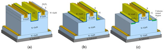
The schematic of the F-plasma-treated quasi-vertical GaN-based trench gate MOSFETs is shown in Figure 1. The traditional device A adopts a gate-in-the-middle structure without F-plasma treatment, while the traditional device B employs a gate-on-both-sides structure, also without F-plasma treatment. Since the gate-in-the-middle structure prevents F-plasma treatment due to the shielding effect of the gate metal, the gate-on-both-sides structure was selected for F-plasma treatment, as shown in Figure 1c. From bottom to top, the main structural parameters of the device are as follows: a 1 µm N+-GaN layer [Si:3 × 1018 cm−3], a 4 µm N−-GaN drift layer [Si:1 × 1016 cm−3], a 350 nm P-GaN layer [Mg:1 × 1019 cm−3], and a 220 nm N+-GaN layer [Si:1 × 1019 cm−3]. The device manufacturing process begins with the etching of a 700 nm deep trench using a Cl2/BCl3 gas mixture in a 15 W inductively coupled plasma (ICP) etching system. After the trench is formed, a 25% TMAH solution is used for a 1 h water bath treatment at 80 °C. The device is then annealed at 700 °C for 10 min to activate the buried P-GaN. Subsequently, a 50 nm thick Al2O3 layer is deposited as the gate dielectric using atomic layer deposition (ALD). The source and drain are made with Ti/Al/Ni/Au as the ohmic metal, while Ni/Au (45 nm/400 nm) is used as the gate metal. Finally, F-plasma treatment is performed to complete the device fabrication. The F-plasma treatment process involves 150 s of CF4 plasma treatment using the ICP system, with a CF4 gas flow rate of 45 sccm, an ICP power of 180 W, and a bias power of 55 W during the treatment.
Figure 1.
(a) Structure diagrams of traditional device A. (b) Structure diagrams of traditional device B. (c) Structure diagrams of F-plasma-treated quasi-vertical GaN-based trench gate MOSFETs.
3. Results
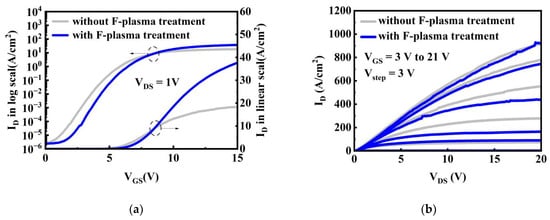
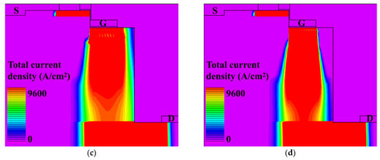
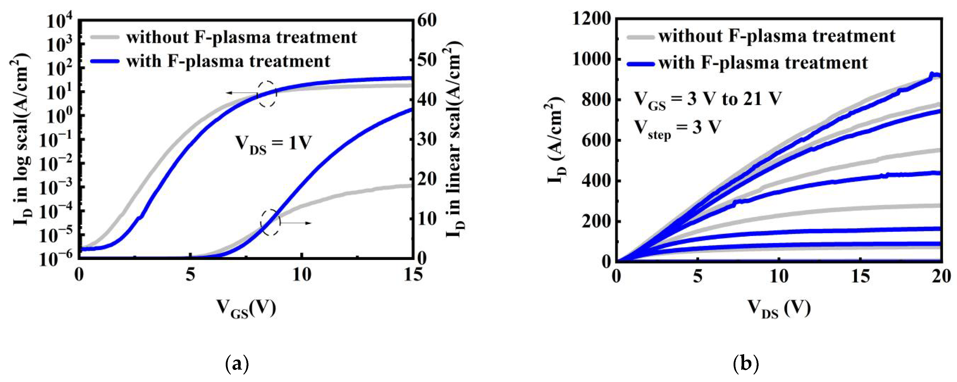
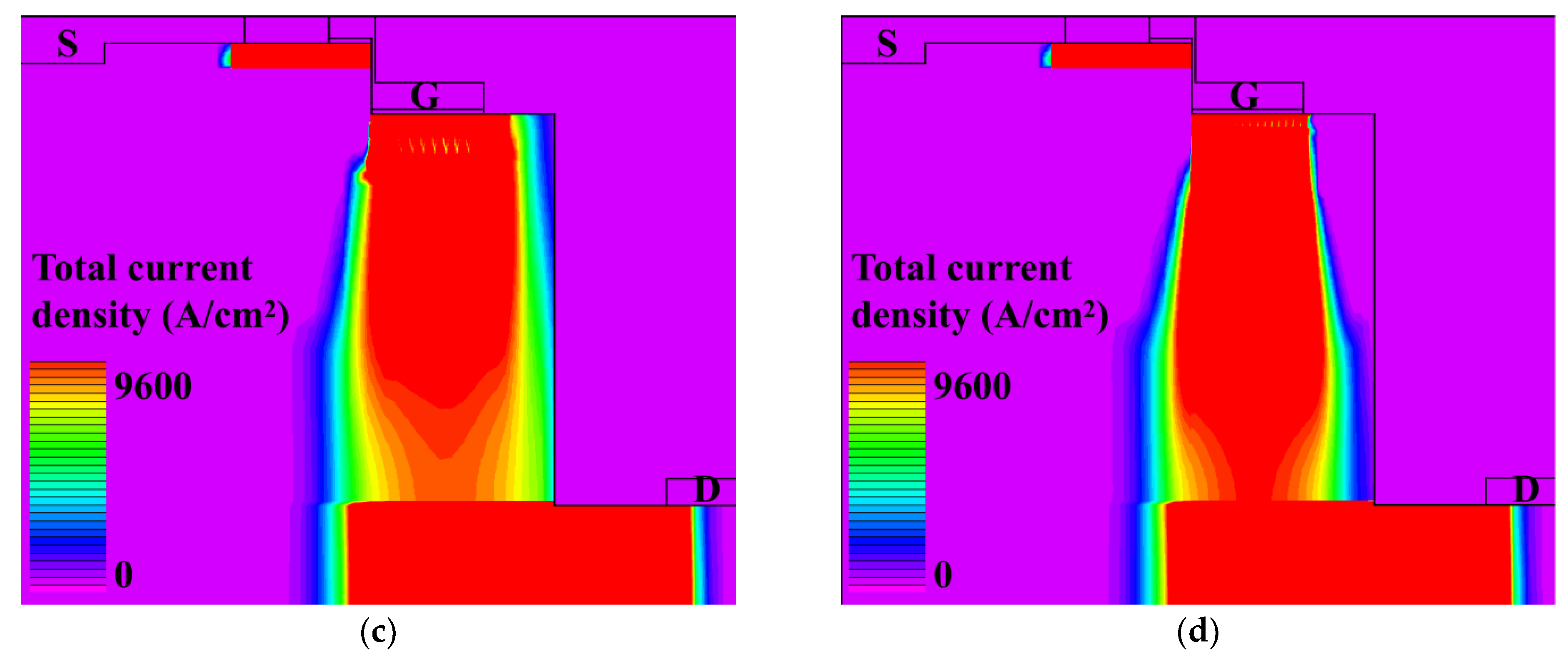
Figure 2a,b compare the transfer and output characteristics of the as-fabricated quasi-vertical GaN-based trench-gate MOSFETs with and without F-plasma treatment. The test device features a total gate trench dimension of 8 µm × 135 µm. As depicted in Figure 2a, the threshold voltages of the untreated and F-plasma-treated samples are measured as 5.8 V and 6.4 V, respectively. Both devices achieve an on/off current ratio (Ion/Ioff) on the order of 105. As shown in Figure 2b, the saturation current of the F-plasma-treated quasi-vertical GaN MOSFETs is lower than that of the untreated counterparts. Nevertheless, at a high gate bias of 21 V, the gap in saturation current becomes negligible, with both devices delivering a current density of approximately 917 A/cm2. Figure 2c,d illustrate the on-state current distribution in the quasi-vertical GaN-based trench-gate MOSFETs with and without F-plasma treatment. The results indicate that the fixed negative charges introduced by F-plasma treatment repel electrons and induce a local depletion region, which accounts for the reduced saturation current. With a scaled-down gate trench size, the device yields a maximum saturation current of 2258.2 A/cm2 and a specific on-resistance (Ron,sp) of 7.2 mΩ·cm2.
Figure 2.
Comparison of (a) transmission and (b) output characteristics of F-plasma-treated and untreated devices based on simulation. Current density distributions of the device (c) without and (d) with F-plasma treatment at VGS = 20 V and VDS = 20 V based on simulation.
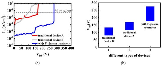
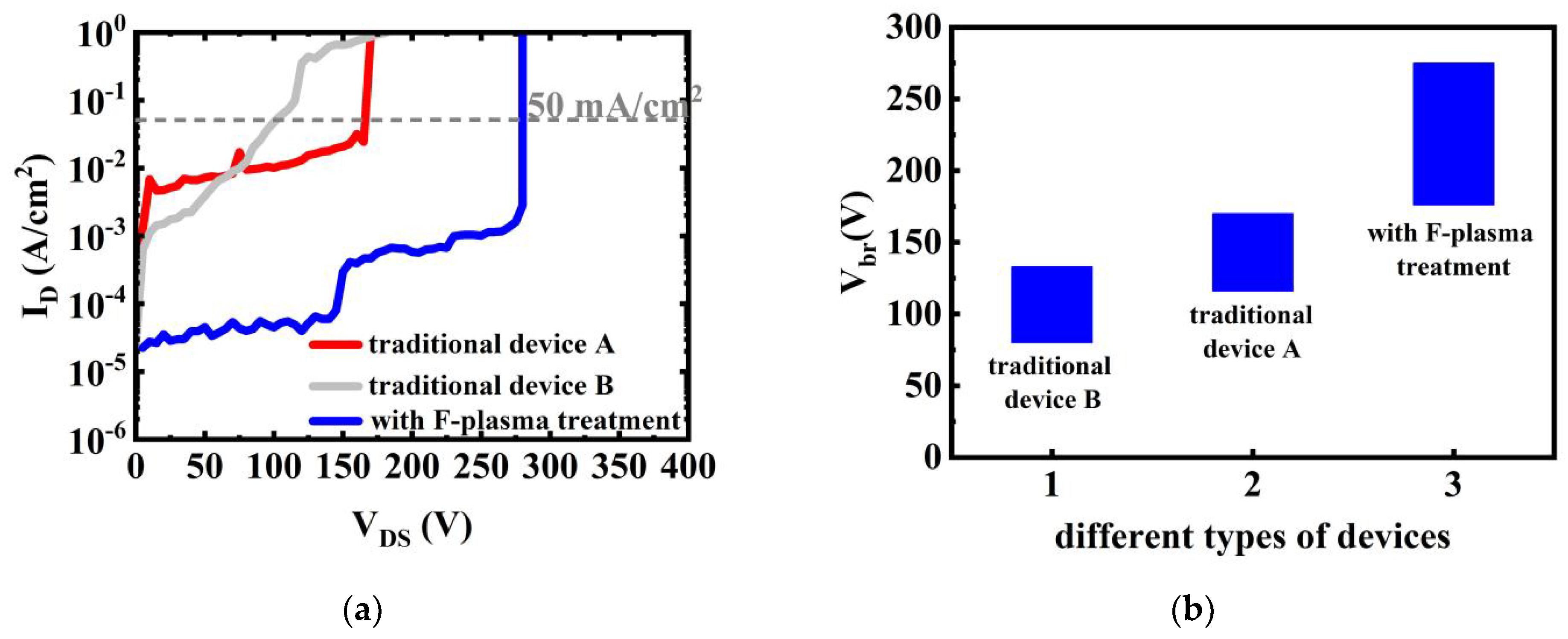
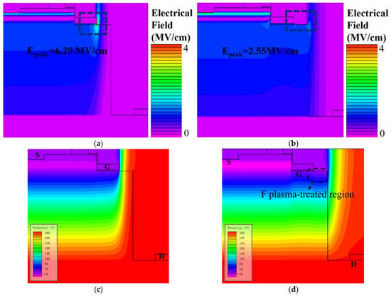
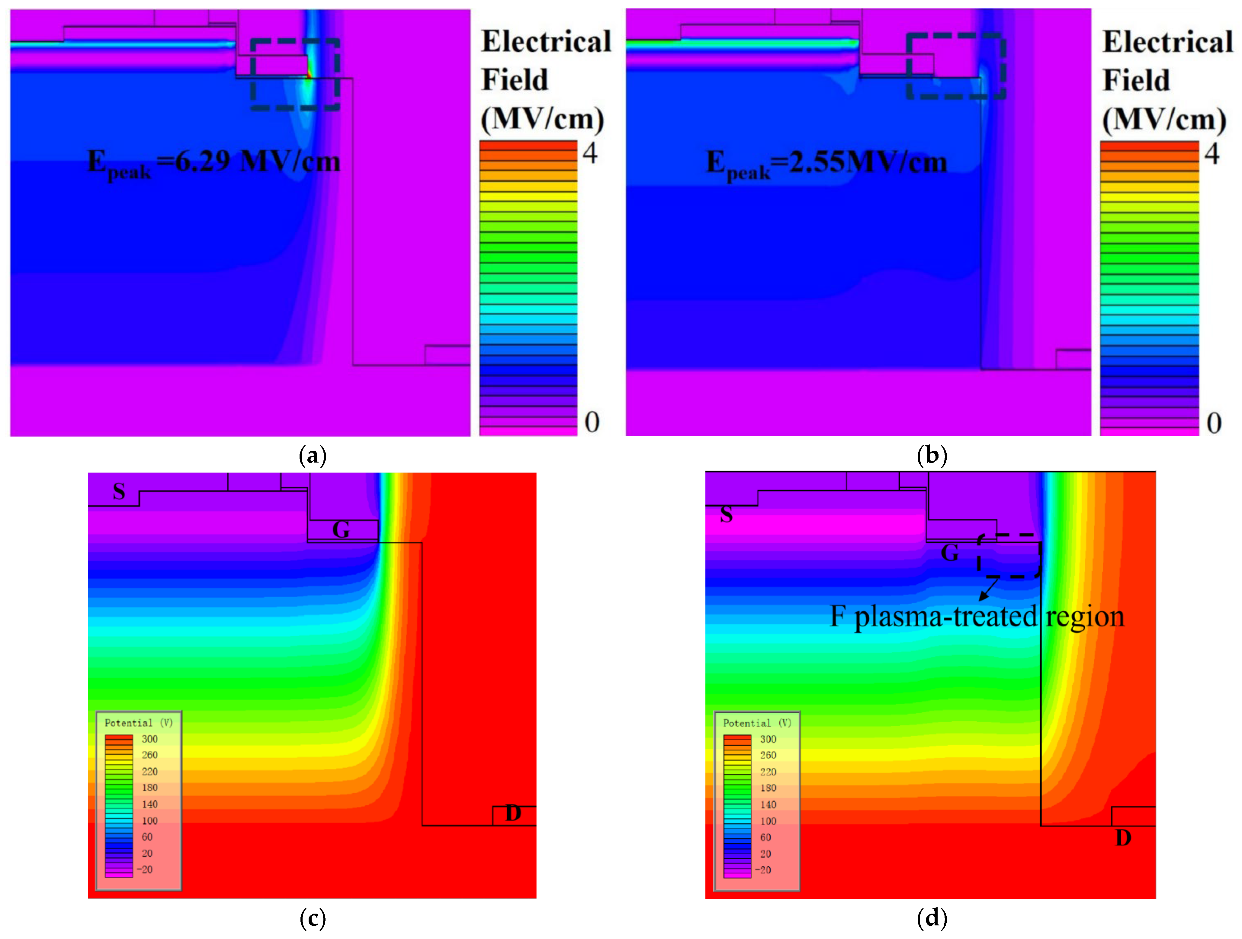
The off-state characteristics of the as-fabricated quasi-vertical GaN-based trench-gate MOSFETs are plotted in Figure 3. The measured breakdown voltages (Vbr) of conventional device A, conventional device B, and the F-plasma-treated device are 170 V, 100 V, and 275 V, respectively. The degraded Vbr of device B relative to device A originates from the reduced gate-to-drain spacing and the deeply etched drift region sidewall: the elevated etching power induces more severe etching damage, rendering the device more susceptible to premature breakdown. With F-plasma treatment, the pre-breakdown leakage current is substantially suppressed, and the resulting Vbr far exceeds those of both conventional devices A and B. This improvement stems from the fixed negative charges introduced in the F-plasma-treated region, which repel electrons and induce a depletion region. This effect serves to spread the electric field distribution and suppress the peak electric field magnitude [16,17]. Figure 3b summarizes the statistical distribution of Vbr measured across different devices. Figure 4a,b depict the potential profiles of devices with and without F-plasma treatment. Simulations reveal that the potential within the F-plasma-treated region is significantly lowered compared with the untreated counterpart, verifying that the incorporated fixed negative charges effectively reduce the local potential and flatten the potential distribution. Figure 4c,d display the off-state electric field distribution in the reference and F-plasma-treated devices under a drain bias of 300 V. The peak electric field drops from 6.29 MV/cm to 2.55 MV/cm, and the severe electric field crowding at the trench gate is effectively mitigated. The combined reduction in gate potential and peak electric field accounts for the enhanced breakdown performance.
Figure 3.
(a) Off-state characteristic curve of the quasi-vertical MOSFET device. (b) Voltage distribution map of the tested device (VGS = 0 V).
Figure 4.
Simulation potential distribution of device (a) without and (b) with F-plasma treatment at 300 V. Simulation of electric field distribution of device (c) without F-plasma treatment and (d) with F-plasma treatment at 300 V.
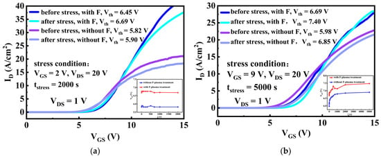
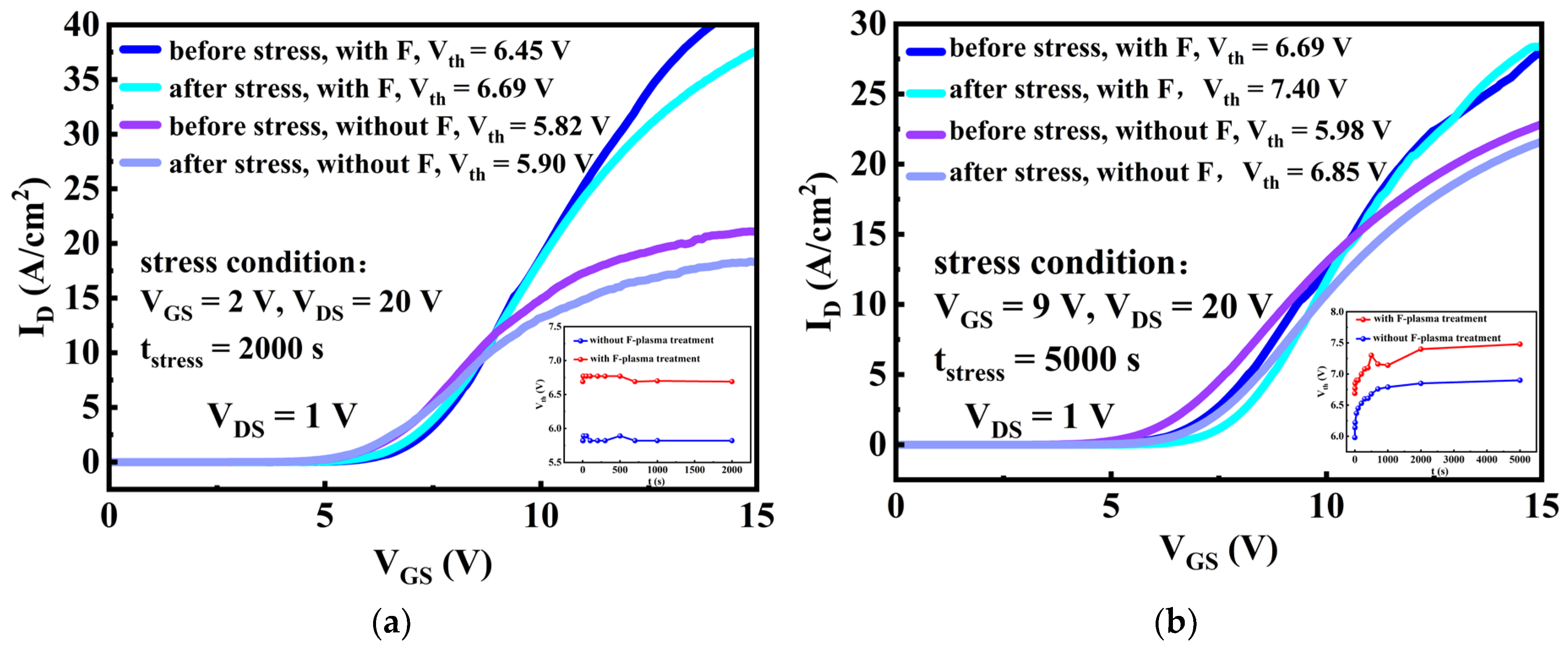
Figure 5a compares the transfer characteristics of the untreated and F-plasma-treated devices before and after off-state stress. Off-state stress shows negligible effect on the threshold voltage of both devices. Figure 5b presents the transfer characteristics of the two devices before and after on-state stress. After 5000 s of on-state stress, the threshold voltage of the untreated device increases by 0.87 V, while that of the F-plasma-treated device rises by 0.71 V. For both devices, the threshold voltage first increases and then stabilizes with increasing stress time. A similar rise in threshold voltage with extended on-state stress time has also been reported by Zhu et al. [18]. Based on the variation trend and amplitude of the threshold voltage, F-plasma treatment introduces almost no additional effects on the device under stress conditions. This is because the F-plasma-treated region is located far from the inversion channel and does not affect the inversion layer. It can be inferred that F-plasma treatment has minimal impact on stable device operation under prolonged on-state conditions. The significant effect of on-state stress on quasi-vertical GaN-based trench gate MOSFETs is speculated to arise from the following mechanism: under high gate stress, trap states may be generated or activated at the interface between the gate dielectric and GaN. These traps capture charge carriers, thereby reducing the gate controllability of the device.
Figure 5.
(a) Comparison of transfer characteristics before and after off-state stress (2000 s) for the device without and with F-plasma treatment and variation in device threshold voltage with off-state stress time for the device with and without F-plasma treatment. (b) Comparison of transfer characteristics before and after on-state stress (5000 s) for the device with and without F-plasma treatment and variation in device threshold voltage with on-state stress time for the device with and without F-plasma treatment.
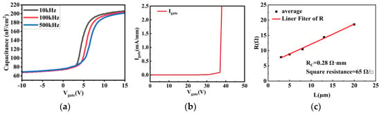
Figure 6a shows the results of the CV test for the device. The CV test allows for the evaluation of the device’s gate control capability and the thickness of the gate dielectric. The measured capacitance is the gate dielectric capacitance, and the gate dielectric thickness can be calculated using its theoretical dielectric constant and gate capacitance. The calculated alumina thickness from the CV test results is 41.7 nm. As can be seen from Figure 6b, the breakdown voltage of the alumina dielectric is 37 V, leading to a breakdown field strength of approximately 8.87 MV/cm. Figure 6c shows that the contact resistance RC measured by TLM is 0.4 Ω·mm, and the ohmic contact resistance RC measured is 0.28 Ω·mm. This result demonstrates that both the deposited dielectric film and the fabricated ohmic contact achieve favorable quality in the present experiment.
Figure 6.
(a) The curve of the CV test for the device. (b) Breakdown curve of alumina dielectric. (c) TLM graphical measurement results of the device.
4. Discussion
This paper presents the fabrication of F-plasma-treated quasi-vertical GaN-based trench-gate MOSFETs and investigates the impact of F-plasma treatment on their electric field distribution and potential profiles. The results show that F-plasma treatment modulates the electric field distribution at the gate region, effectively reducing the peak electric field strength. Compared with untreated devices, the peak electric field of the treated device is reduced from 18.7 MV/cm to 4.08 MV/cm. With F-plasma treatment, the breakdown voltage of the fabricated device is successfully increased from 170 V to 275 V. Stress test results indicate that the threshold voltage of both treated and untreated devices is affected by interface charges and traps, and F-plasma treatment imposes no additional impact on the threshold voltage stability of the device. It is expected that under prolonged on-state operation, the treatment will have minimal influence on stable device performance. The foregoing results indicate that F-plasma treatment represents a promising approach worthy of investigation for both gate-controlled channel devices operating at high voltage, high frequency or high power and devices with gate oxides prone to electric field-induced degradation. The F-plasma-treated quasi-vertical GaN-based trench gate MOSFETs are expected to have a significant impact on medium- and high-voltage applications.
Supplementary Materials
The following supporting information can be downloaded at: https://www.mdpi.com/article/10.3390/mi17091019/s1, Table S1. GaN material simulation parameter table.
Author Contributions
Conceptualization, P.Z.; Methodology, P.Z. and B.H.; Software, D.-Y.L.; Validation, D.-Y.L.; Formal analysis, J.-R.X. and Q.-Y.C.; Resources, P.Z. and Q.-Y.C.; Data curation, D.-Y.L. and J.-R.X.; Writing—original draft, D.-Y.L. and J.-R.X.; Writing—review & editing, P.Z.; Supervision, B.H. and H.X.; Project administration, H.X.; Funding acquisition, X.-H.M. All authors have read and agreed to the published version of the manuscript.
Funding
This work was supported by the National Natural Science Foundation of China under Grant No. 62188102.
Institutional Review Board Statement
Not applicable.
Informed Consent Statement
Not applicable.
Data Availability Statement
The original contributions presented in this study are included in the article/Supplementary Materials. Further inquiries can be directed to the corresponding authors.
Conflicts of Interest
The authors declare no conflict of interest.
References
- Zhu, R.Q.; Jiang, H.X.; Tang, C.W.; Lau, K.M. GaN quasi-vertical trench MOSFETs grown on Si substrate with ON-current exceeding 1 A. Appl. Phys. Express 2022, 15, 121004. [Google Scholar] [CrossRef] [Scilit]
- Ji, D.; Gupta, C.; Chan, S.H.; Corrion, A.; Brown, D.; Wong, J.; Schmitz, A.; Fung, H.; Kim, S.; Micovic, M. Demonstrating >1.4 kV OG-FET performance with a novel double field-plated geometry and the successful scaling of large-area devices. In Proceedings of the IEEE International Electron Devices Meeting, San Francisco, CA, USA, 2–6 December 2017. [Google Scholar] [CrossRef] [Scilit]
- Ji, D.; Gupta, C.; Agarwal, A.; Chan, S.H.; Brown, D.; Wong, J.; Schmitz, A.; Fung, H.; Kim, S.; Micovic, M. Large-Area In-Situ Oxide, GaN Interlayer-Based Vertical Trench MOSFET (OG-FET). IEEE Electron Device Lett. 2018, 39, 711. [Google Scholar] [CrossRef] [Scilit]
- Gupta, C.; Lund, C.; Chan, S.H.; Ji, D.; Brown, D.; Wong, J.; Schmitz, A.; Fung, H.; Kim, S.; Micovic, M. In Situ Oxide, GaN Interlayer-Based Vertical Trench MOSFET (OG-FET) on Bulk GaN substrates. IEEE Electron Device Lett. 2017, 38, 353. [Google Scholar] [CrossRef] [Scilit]
- Zhu, R.Q.; Jiang, H.X.; Tang, C.W.; Lau, K.M. Effects of p-GaN Body Doping Concentration on the ON-State Performance of Vertical GaN Trench MOSFETs. IEEE Electron Device Lett. 2021, 42, 970. [Google Scholar] [CrossRef] [Scilit]
- Zhu, R.Q.; Jiang, H.X.; Tang, C.W.; Lau, K.M. Enhancing ON- and OFF-State Performance of Quasi-Vertical GaN Trench MOSFETs on Sapphire with Reduced Interface Charges and a Thick Bottom Dielectric. IEEE Electron Device Lett. 2022, 43, 346. [Google Scholar] [CrossRef] [Scilit]
- Yin, Y.D.; Pinchbeck, J.; O’Regan, C.; Zhang, S.; Zhang, Y.; Shen, H.; Sun, Y.; Liu, H.; Wang, Z.; Zhang, B.; et al. Fabrication of Semi-Polar (11-22) GaN V-Groove MOSFET Using Wet Etching Trench Opening Technique. IEEE Electron Device Lett. 2022, 43, 1641. [Google Scholar] [CrossRef] [Scilit]
- Khadar, R.A.; Liu, C.; Soleimanzadeh, R.; Matioli, E. Fully Vertical GaN-on-Si power MOSFETs. IEEE Electron Device Lett. 2019, 40, 443. [Google Scholar] [CrossRef] [Scilit]
- Liu, C.; Khadar, R.A.; Matioli, E. GaN-on-Si Quasi-Vertical Power MOSFETs. IEEE Electron Device Lett. 2018, 39, 71. [Google Scholar] [CrossRef] [Scilit]
- Binder, A.T.; Steinfeldt, J.; Reilly, K.J.; Casady, J.B.; Hite, J.K.; Eddy, C.R.; Armstrong, A.M.; Hefner, A.R.; Pearton, S.J.; Jena, D. High current density 1.2 kV class HfO2-gated vertical GaN trench MOSFETs. Appl. Phys. Express 2024, 17, 101003. [Google Scholar] [CrossRef] [Scilit]
- Jaiswal, N.K.; Ramakrishnan, V.N.; Roy, S.D. Vertical GaN Split Gate Trench MOSFET with Improved High Frequency FOM. In Proceedings of the IEEE 17th India Council International Conference, New Delhi, India, 10–13 December 2020. [Google Scholar] [CrossRef] [Scilit]
- Zhou, K.N.; Shan, L.Q.; Zhang, Y.L.; Wang, Y.; Li, W.; Li, H.; Wang, Z.; Hao, Y. Fluorine Plasma Treatment for AlGaN/GaN HEMT-Based Ultraviolet Photodetector With High Responsivity and High Detectivity. IEEE Electron Device Lett. 2023, 44, 781. [Google Scholar] [CrossRef] [Scilit]
- Li, Y.J.; Yang, S.; Liu, K.; Lin, Y.; Zhang, Y.; Sun, X.; Wang, Z.; Hao, Y. Fully-Vertical GaN-on-SiC Schottky Barrier Diode: Role of Conductive Buffer Structure. IEEE Trans. Electron Dev. 2023, 70, 619. [Google Scholar] [CrossRef] [Scilit]
- Jia, F.C.; Ma, X.H.; Yang, L.; Li, S.; Li, W.; Li, H.; Wang, Z.; Hao, Y. 930V and Low-Leakage Current GaN-on-Si Quasi-Vertical PiN Diode with Beveled-Sidewall Treated by Self-Aligned Fluorine Plasma. IEEE Electron Device Lett. 2022, 43, 1400. [Google Scholar] [CrossRef] [Scilit]
- Chen, J.B.; Song, X.F.; Liu, Z.H.; Li, W.; Li, H.; Wang, Z.; Hao, Y. A GaN-on-Si quasi-vertical Schottky barrier diode with enhanced performance using fluorine ion-implanted field rings. Appl. Phys. Express 2021, 14, 116504. [Google Scholar] [CrossRef] [Scilit]
- Kim, Y.S.; Lim, J.Y.; Kim, M.K.; Han, M.K. High breakdown voltage AlGaN/GaN HEMT by employing selective fluoride plasma treatment. Phys. Status Solidi C 2010, 8, 453–456. [Google Scholar] [CrossRef] [Scilit]
- Chu, R.; Shen, L.; Fichtenbaum, N.; Brown, D.; Keller, S.; Mishra, U.K. Plasma Treatment for Leakage Reduction in AlGaN/GaN and GaN Schottky Contacts. IEEE Electron Device Lett. 2008, 29, 297–299. [Google Scholar] [CrossRef] [Scilit]
- Zhang, Y.; Zhu, R.Q.; Qu, H.L.; Jiang, H.X.; Tang, C.W.; Lau, K.M. Dynamic Reliability Assessment of Vertical GaN Trench MOSFETs with Thick Bottom Dielectric. IEEE Trans. Device Mater. Reliab. 2024, 24, 358. [Google Scholar] [CrossRef] [Scilit]
Disclaimer/Publisher’s Note: The statements, opinions and data contained in all publications are solely those of the individual author(s) and contributor(s) and not of MDPI and/or the editor(s). MDPI and/or the editor(s) disclaim responsibility for any injury to people or property resulting from any ideas, methods, instructions or products referred to in the content. |
© 2026 by the authors. Licensee MDPI, Basel, Switzerland. This article is an open access article distributed under the terms and conditions of the Creative Commons Attribution (CC BY) license.