


Abstract
Two-dimensional transition-metal carbides and nitrides (MXenes) are increasingly adopted in advanced electronic devices, where their metallic conductivity, optical tunability, and chemically addressable surfaces support next-generation multifunctional optoelectronics. Their practical performance, however, depends not only on their intrinsic properties but also on the heterogeneous interfaces where charges, photons, and ions interact. Unlike earlier reviews organized around synthesis routes or separate device categories, this review takes interfacial chemistry as a single organizing principle and follows it from surface terminations through to integrated systems. The structural and surface-chemical characteristics of MXenes are described first, showing how dynamic terminations and interfacial dipoles regulate work functions and energy-level alignment. We then discuss molecular functionalization, defect passivation, and heterojunction formation as strategies for reducing Schottky barriers and improving charge-transfer kinetics. Optoelectronic platforms built on these engineered interfaces, including high-efficiency photovoltaics, broadband photodetectors, and stretchable wearable systems, are subsequently detailed, together with emerging architectures that merge self-powered sensing with neuromorphic visual functions, a scope seldom treated alongside conventional devices in previous surveys. By connecting surface chemistry with device integration, this review outlines a materials-to-systems pathway toward more reliable and scalable MXene-based optoelectronic technologies.
1. Introduction
Optoelectronic technology has advanced quickly in recent years, and with it the way light, electricity, and information are generated, transported, detected, and interpreted. Transparent electrodes [1,2,3,4,5,6], photovoltaics [7,8,9,10,11,12,13,14], photodetectors [15,16,17,18,19,20,21,22,23,24,25,26,27,28,29], light-emitting devices [3,4,30,31,32], wearable sensors [33,34,35,36], and neuromorphic visual systems [37,38,39] are rarely developed in isolation anymore. They are instead combined into platforms that convert energy, transduce signals, carry optical communication [40], and interact directly with users. Such integration places heavy demands on the constituent materials, which must deliver high electrical conductivity, optical tunability [28,41], mechanical compliance [34,35], solution processability [41,42], and chemically programmable interfaces at the same time. Conventional transparent conductors and interfacial layers, including indium tin oxide, noble metals, metal oxides, and carbon-based nanomaterials, have contributed substantially to the development of modern optoelectronics [27,30]. Nevertheless, their intrinsic limitations, such as mechanical brittleness [32], limited work function tunability [14,30], interfacial incompatibility, high processing cost, or insufficient chemical adaptability, continue to restrict the realization of flexible, scalable, and multifunctional optoelectronic systems [31,39].
Two-dimensional transition-metal carbides, nitrides, and carbonitrides, collectively termed MXenes, have emerged as a distinctive class of materials that may bridge this gap [40,43,44]. First synthesized in 2011 from the Ti3AlC2 MAX phase, MXenes follow the general formula Mn+1XnTx, where M is an early transition metal, X is carbon or nitrogen, and Tx represents surface termination groups [45]. Unlike semiconducting two-dimensional materials, MXenes possess energy bands that cross the Fermi level [46,47], enabling metal-like charge transport even in optically semi-transparent ultrathin films [43,48,49,50]. MXenes also disperse readily in water or polar solvents as colloids, which opens the way to low-temperature spray [51], blade, and inkjet deposition [52], while their laminar stacking allows the interlayer spacing and the dielectric response to be adjusted by intercalation [53,54]. These characteristics position MXenes at an intersection of conductivity, optical activity, and chemical addressability that the optoelectronics field had previously been unable to access within a single material system [40,49,55,56].
These claims are best assessed against the two-dimensional materials that preceded MXenes. Graphene owes its conduction to π bonding within the sp2 lattice and reaches a resistivity near 10−8 Ω m, but only in ideal single-layer form rather than in the solution-processed films on which scalable fabrication depends. Graphene oxide falls well short of even that practical level, since the rise in sp3 character removes the conducting π network and drives the resistivity to roughly 108 Ω m, so a thermal or chemical reduction step is required before the material conducts at all. Ti3C2Tx needs no such recovery step and reaches 15,100 S/cm in solution-cast film, the highest value reported for a solution-processed two-dimensional solid [57,58,59]. The same contrast holds in transparent-electrode geometry, where aligned Ti3C2Tx flakes transmitting above 90% of visible light give a sheet resistance near 1032 Ω/sq, about one-third of the graphene value at comparable transparency. More important here, these figures are not fixed by the parent composition. Termination chemistry alone carries the work function from 1.6 eV for hydroxyl-terminated Sc2C to 4.60 eV for Ti3C2 and 5.1 eV for an oxygen-rich surface, a span graphene cannot match while pinned near 4.5 eV [60,61,62].
The optoelectronic relevance of MXenes, however, is not limited to their metallic conduction [63,64]. MXene films exhibit composition-dependent extinction [51,55,65], transmittance, and plasmonic resonances spanning the ultraviolet to the mid-infrared [44,56,66,67,68], all of which shift with flake thickness [69,70], carrier concentration, and surface termination without requiring changes in chemical composition [47,65,71,72,73]. More consequentially for device integration, surface terminations such as –O, –OH, –F, and –Cl alter both the local dielectric environment and the Fermi level simultaneously, coupling the photonic and electronic responses of MXene into a single tunable system [47,54,65,74,75,76,77,78,79,80,81,82,83,84]. This built-in coupling between photons and electrons sets MXenes apart from ordinary conductive additives. It also means they are better regarded as optically active metallic two-dimensional materials, with optoelectronic functions that can be engineered on purpose rather than simply taken advantage of [68,85].
The chemistry of the heterogeneous interface, however, carries the greatest consequence for the integration of MXenes into optoelectronic devices [86]. Surface terminations should not be regarded as passive residues of the synthesis [87,88]. Theoretical and experimental studies agree that the work function of Ti3C2Tx can be shifted reproducibly over a wide range by controlling the termination composition [80,84,87,89,90,91,92,93], by noncovalent molecular doping [94,95,96], or by covalent functionalization with electron-withdrawing or electron-donating organic groups [97,98,99,100,101]. Such adjustments carry immediate consequences for device physics. A mismatch in energy-level alignment at a semiconductor heterojunction may turn an Ohmic contact into a rectifying Schottky junction or introduce Fermi-level pinning that quenches the photovoltage, whereas accurate alignment permits selective carrier extraction and suppresses recombination [87,101,102,103,104,105,106]. The influence of MXene surfaces is not confined to energy-level engineering. Lewis-acidic Ti centers and oxygen-containing terminations coordinate with unpassivated surface metal ions [13,100,107], fill vacancies in oxide charge transport layers [108,109], and chelate dangling bonds, thereby suppressing nonradiative recombination and retarding ionic migration at the same time. This dual character, an electronically adaptive contact that also acts as a chemically passivating interfacial layer, separates MXene surface engineering from conventional conductive interlayers and has brought interfacial design to the center of high-performance MXene optoelectronics [110].
These interfacial principles have been examined across a broad range of device platforms. MXene-modified charge transport layers in photovoltaics [111] suppress recombination and stabilize the interfaces, with gains in both efficiency and operational lifetime [7,8,9,10,11,12,13,14]. Photodetectors exploit the work function contrast at MXene–semiconductor Schottky junctions, where the resulting built-in electric fields support self-powered broadband operation from the ultraviolet to the near-infrared [15,16,17,18,19,20,21,22,23,24,25,27,29,32,35]. Light-emitting and flexible display systems benefit from MXene electrodes of tunable work function, which assist carrier injection while their mechanically compliant film-forming behavior sustains operation under repeated deformation [3,4,30,31,33,49]. Neuromorphic architectures make use of MXene-derived dielectric layers that provide photocarrier trapping and multilevel conductance modulation, emulating biological synaptic plasticity [38,39]. Considerable obstacles nevertheless persist. Ambient oxidation degrades both the conductivity and the reproducibility of the surface dipole [33,39], fluoride-based synthesis yields stochastic termination distributions that complicate interfacial control [14,38], and the formulation of scalable inks with suppressed interlayer restacking calls for further process engineering [26,34,42].
The present review surveys recent progress in multifunctional MXene-based materials, taking as its unifying theme the transition from fundamental interfacial engineering to robust device integration, as outlined schematically in Figure 1. Structural and surface-chemical foundations are treated first, followed by work function tuning [30,31,32,93], energy-level alignment [13,96], Schottky barrier modulation [27,29,41,101,104,112], and defect passivation strategies [13,38,104,108,109]. Representative device platforms are then considered, covering photovoltaics [7,8,9,10,11,12,14], photodetectors [15,16,17,18,19,20,21,22,23,24,25,29,34], light-emitting systems [3,4,30,31], wearable optoelectronics [33,36], and neuromorphic visual interfaces [28,37,39,41]. A concluding perspective addresses fluorine-free synthesis, oxidation-resistant design, and scalable processing toward reliable MXene-based optoelectronic technologies [105,113].
Figure 1.
Schematic illustration of interfacial engineering and optoelectronic applications of multifunctional MXenes.
2. Fundamental Properties and Interfacial Chemistry
2.1. Optical and Plasmonic Properties
The optical response of MXenes arises from the interplay between the free carriers of a metallic transition-metal carbide or nitride lattice and the surface terminations that cover each atomically thin sheet, both of which can be tailored through composition and processing [114,115,116]. This tunability endows MXenes with an optical behavior that spans transparent conduction [48,50,115], broadband absorption [71,117], and wavelength-selective reflection [46,117] across the ultraviolet, visible, and infrared, making them attractive for optoelectronic and photothermal devices while also complicating the interpretation of their characteristic spectral features [40,118,119]. Establishing how these features depend on composition, carrier density, and surface chemistry is therefore a prerequisite for their rational design.
Gogotsi and co-workers surveyed nine carbide MXenes and showed that their optical response is governed primarily by composition (Figure 2a–d). The gravimetric extinction spectra display a strong, compositionally insensitive absorption in the UV together with a characteristic visible-to-NIR peak whose position is set by the atomic structure. Reducing the layer number from Ti3C2 to Ti2C, or substituting Ti with Mo, systematically pushes this peak toward higher energy (Figure 2a). The thin-film transmittance divides the MXenes into two families (Figure 2b). In one group, the NIR transmittance increases with wavelength, whereas in the other, it decreases. This latter group, comprising the highly conductive V2C, Ti2C, and Ti3C2, shows a negative slope indicative of metallic reflection that emerges near the wavelength at which the real part of the dielectric function turns negative, as expected for a Drude-like free-carrier plasma. This interpretation is supported by p-polarized reflectance (Figure 2c), where the onset of strong reflection coincides with the decline in transmittance.
Figure 2.
(a) UV-vis-NIR optical extinction properties of 2D transition metal carbides measured for colloidal solutions. (b) UV-vis-NIR transmittance spectra for MXene thin films. (c) Reflectance spectra of Ti3C2, Ti2C, and V2C films measured at a 75° incident angle using p-polarized light. (d) Normalized extinction spectra of Ti3C2 and Ti2C colloidal solutions synthesized via HF/TMAOH or HF/HCl/LiCl. Reproduced with permission from Ref. [51]. Copyright (2020), Wiley-VCH GmbH. (e) Schematic illustration of the high solar absorptance, high mid-infrared reflectance, and low infrared emissivity of MXene. (f) Absorptance/emissivity spectrum of Ti3C2Tx MXene (red) with solar (yellow) and thermal radiation (blue) spectra. (g) Real (ε1) part of the in-plane permittivity of Ti3C2Tx with different surface terminations. (h) Absorptance/emissivity spectra of Ti3C2Tx with different terminations. Reproduced with permission from Ref. [117]. Copyright (2021), Wiley-VCH GmbH.
The reflectance maximum of Ti3C2 moreover aligns closely with the plasmon energy-loss peak obtained from STEM-EELS, pointing to a common plasmonic origin for the reflectance and extinction features. A key prediction of this plasmonic picture is that the peak should shift to higher energy as the free-carrier density rises. In accordance with this, replacing the conventional HF etchant with a mixed-acid (HF/HCl) route and LiCl intercalation blue-shifts the extinction peaks of both Ti2C and Ti3C2 (Figure 2d), consistent with a carrier-concentration–dependent plasmon resonance [51].
Beyond broadband optical absorption, MXenes exhibit pronounced spectral selectivity that enables efficient solar–thermal conversion with suppressed infrared heat loss. Li et al. demonstrated that Ti3C2Tx behaves as a visible-black but infrared-white selective absorber, strongly absorbing incident solar radiation while reflecting mid-infrared thermal radiation (Figure 2e). The freestanding Ti3C2Tx film exhibited a solar absorptance of approximately 90% and a thermally weighted infrared emissivity of only 17% at 100 °C (Figure 2f), with values as low as approximately 10% achieved for surfaces with more favorable nanosheet alignment. This combination reduces radiative heat loss and improves solar–thermal energy retention without requiring a lithographically patterned metasurface.
First-principles calculations further revealed that this spectral selectivity is strongly governed by surface termination (Figure 2g,h). The complex permittivity of uniformly terminated Ti3C2Tx models was obtained from density functional theory with a hybrid functional, and the normal-incidence reflectance was evaluated through the Fresnel relation, with the absorptance taken as unity minus the reflectance for optically thick films. Because the electric field lies in the basal plane, the in-plane dielectric response dominates reflection from the layered film. The real permittivity of Ti3C2F2 and Ti3C2(OH)2 becomes negative in the near-infrared region and increases substantially in magnitude at longer wavelengths, indicating a strong metallic response that enhances mid-infrared reflection. These fluorine- and hydroxyl-terminated MXenes therefore retain high absorption across the solar spectrum while exhibiting substantially lower infrared emissivity than pristine Ti3C2 and Ti3C2O2. Such models nevertheless assume a single termination species on an ideal periodic surface, whereas etched films carry disordered mixtures of −O, −OH, and −F together with vacancies and intercalated water, which explains why the predicted spectra reproduce experimental trends without matching them quantitatively. Quantitative prediction will require configurational averaging over mixed terminations, along with validation against measured optical constants [117].
Additionally, the physical origin of the near-infrared extinction feature in Ti3C2Tx remains under debate. Spectroscopic ellipsometry, combined with density functional theory in which the interband optical conductivity is constructed from maximally localized Wannier functions and the intraband part is added through a Drude term, attributes the broad feature near 1.5 eV to an interband transition rather than to a localized plasmon resonance. The transition connects nearly flat bands close to the Γ point of oxygen-terminated Ti3C2O2, and the only well-defined surface plasmon polariton is predicted near 0.5 eV, outside the optical window. Supporting evidence comes from the near disappearance of the feature in chlorine-terminated Ti3C2Cl2 and from the positive real permittivity measured at 1.5 eV, which cannot sustain a plasmonic mode. Because such models assume a single termination species and an empirically fixed Hubbard correction for the Ti 3d states, they describe limiting cases rather than films with mixed terminations. The optical spectra of MXenes therefore arise from an interplay between free-carrier and termination-dependent interband contributions rather than from a single universal plasmonic mechanism [65].
Beyond surface termination, the optical response of MXenes can also be regulated through the X-site composition of the lattice. First-principles calculations of Ti3CN, with optical spectra evaluated within the Tamm–Dancoff approximation to time-dependent density functional theory, show that partial substitution of carbon by nitrogen preserves metallic band dispersion while leaving a comparatively flat conduction band just above the Fermi level. Parallel band absorption between these features sustains strong broadband absorption extending into the infrared, and the response is further differentiated by O- and F-based terminations. Nonadiabatic molecular dynamics on the same structures links this band arrangement to carrier dynamics, since fluorine- and mixed-terminated models release most of the excess electron energy within roughly 200 fs whereas the O-terminated surface relaxes far more slowly. X-site substitution and termination chemistry thus provide complementary routes for tailoring the electronic and optical characteristics of MXenes [118]. The optical and plasmonic properties of the representative MXenes discussed above are summarized in Table 1, which compiles their composition, characteristic extinction or reflectance features, and the resulting optical functionality across the ultraviolet, visible, and infrared regions.
Table 1.
Structural and optical properties of MXenes.
2.2. Electrical Transport
The same metallic free-carrier system that governs the optical response of MXenes also makes them among the most conductive of all solution-processable two-dimensional materials, underlying their use as electrodes and charge transport layers [50]. This conductivity, however, is not a fixed material constant but is shaped by the transition-metal chemistry and atomic-layer structure [79,120,121], by the surface terminations [80,83,90,122] and confined interflake water [65,69,123,124], and by the degree of oxidation [69,79,125], so that thermal history and processing can either enhance or degrade transport [123,126,127]. Because the optical and electrical responses share a common free-carrier origin [44,46,122,128,129], spectroscopic probes provide a sensitive, contactless route to tracking how these properties evolve during processing [64,125].
Fakhraai et al. [69] investigated the thermal evolution of the optical and electrical properties of MXene thin films using in situ spectroscopic ellipsometry under ambient heating conditions (Figure 3a–d). The measured spectra were reconstructed with a multilayer optical model combining two harmonic oscillators for the interband extinction with a Drude oscillator for the free-carrier response, so that the resistivity is obtained from the same fit that describes the absorption bands. As shown in Figure 3a, the real part of the dielectric function of Ti3C2Tx turns negative near 620 nm, marking the onset of free-carrier oscillations, and Drude fitting of a 14 nm film gives an optical resistivity of 0.0010 ± 0.0001 Ω cm, or 978 ± 10 S/cm. Because the model treats the porous film as an effective medium, this value represents a lower bound on the DC resistivity. Two thermal regimes then emerge from the resistivity and thermogravimetric data (Figure 3b). Heating from about 100 to 245 °C lowers the resistivity through removal of adsorbed and intercalated water, and first-principles calculations attribute the accompanying gain to surface de-functionalization, which raises the density of states at the Fermi level.
Figure 3.
(a) Real (ε1) and imaginary (ε2) components of the dielectric constant of Ti3C2Tx (14 nm film) as a function of wavelength. (b) Optical resistivity and TGA weight change in a Ti3C2Tx film (19 nm film) as a function of temperature. (c) Normalized extinction coefficient (k) spectra of Ti3C2Tx (19 nm film), Ti2CTx (3 nm film), and Mo2TiC2Tx (9 nm film). (d) Temperature-dependent optical resistivity of Ti3C2Tx, Ti2CTx, and Mo2TiC2Tx. Reproduced with permission from Ref. [69]. Copyright (2023), Wiley-VCH GmbH. (e) Conductivity (σ) and scattering time (τ) of Ti3C2Tx films as a function of temperature. (f) Time-dependent photoconductivity changes in Ti3C2Tx for various photon energies (hv) at 287 K. (g) Average photoconductivity extracted from the 3–10 ps delay time range in (f) as a function of photon energy. (h) Accumulated transient reflectivity (ΔR/R) as a function of effective delay time (Δteff). Reproduced with permission from Ref. [130]. Copyright (2026), Springer Nature. (i) Terahertz sheet resistance of Flat (uniform film on quartz) and Wrinkle-I (isotropic wrinkles on PDMS) Ti3C2Tx films across 0.2–1.6 THz. (j) Resistance changes in the Wrinkle-I and Wrinkle-P films during the loading and unloading processes. Reproduced with permission from Ref. [49]. Copyright (2024), Springer Nature. (k) Transmittance at 550 nm versus sheet resistance for Ti3C2Tx thin films fabricated by different methods. (l) Sheet resistance stability of LLIA Ti3C2Tx and commercial ITO-PET as a function of bending cycles. Reproduced with permission from Ref. [43]. Copyright (2021), Springer Nature.
Further heating reverses the trend, since the resistivity rises and the extinction falls as the conductive network degrades through de-functionalization and oxidation to TiO2. The red-shift of the visible–NIR extinction band during this process argues against a plasmonic assignment, because loss of the water dielectric environment would blue-shift a resonance, and it supports interband transitions between closely spaced surface-derived bands, with the intrinsic plasmon predicted near 10 eV. Comparison of Ti3C2Tx, Ti3CTx, and Mo2TiC2Tx shows that transition-metal composition, atomic-layer thickness, and synthesis-derived intercalants govern both conductivity and stability (Figure 3c,d), with oxidation onsets near 450, 300, and 400 °C, respectively. For Mo2TiC2Tx, Drude and Gaussian oscillators fit the data equally well within the accessible spectral window, the latter yielding a 0.06 eV gap close to the value predicted by density functional theory, so the metallic or semiconducting character of this MXene cannot be settled without infrared measurements. Controlled annealing below the oxidation threshold therefore improves conductivity, whereas excessive thermal exposure degrades both optical and electrical performance [69].
Wang et al. [130] investigated photothermal regulation of charge transport in a Ti3C2Tx MXene thin film using terahertz time-domain spectroscopy, optical pump–terahertz probe spectroscopy, and transient reflectance measurements (Figure 3e–h). As shown in Figure 3e, the static terahertz conductivity and carrier scattering time decrease with increasing temperature, whereas the carrier density remains nearly unchanged. Within the Drude framework, σ = Ne2τ/m*, this indicates that conductivity is governed mainly by scattering time and carrier mobility, with electron–phonon scattering as the dominant mechanism. Upon optical excitation, photoconductivity rapidly decreases within a few picoseconds and remains suppressed over nanosecond timescales (Figure 3f). The stronger negative photoconductivity at higher pump photon energies (Figure 3g) shows that absorbed optical energy is transferred to the lattice, increasing phonon populations and carrier scattering.
Transient reflectance measurements confirm the unusually slow thermal relaxation of Ti3C2Tx, with residual heat persisting beyond 100 ns and a thermal decay constant of approximately 40 ns (Figure 3h). Thus, Ti3C2Tx behaves as an efficient phonon heat reservoir, where rapid carrier-to-lattice energy transfer and slow heat dissipation sustain the elevated lattice temperature and prolonged conductivity suppression. This coupled photothermal–electrical response provides a physical basis for MXene-based photothermal electronics, infrared sensing, thermal management, and optoelectronic devices [130].
Structural engineering of MXene films provides an additional route to improve electrical transport and mechanical reliability without sacrificing optical transparency. Gui et al. demonstrated wrinkled Ti3C2Tx films by forming isotropic wrinkle structures on PDMS substrates and periodic longitudinal wrinkles on pre-stretched PDMS substrates (Figure 3i,j). In the terahertz region, the Wrinkle-I film exhibited a lower sheet resistance than the flat film, indicating that the wrinkled architecture enhances effective charge transport by increasing the carrier density and prolonging the scattering time (Figure 3i). More importantly, the Wrinkle-P film maintained stable electrical pathways under mechanical deformation, showing only a modest resistance increase even at 40% tensile strain (Figure 3j). This behavior suggests that periodic wrinkles can accommodate external strain through structural unfolding, thereby preserving the conductive MXene network and improving the durability of flexible optoelectronic films [49].
For transparent electrode applications, Ling et al. introduced a liquid/liquid interfacial self-assembly method to construct highly uniform Ti3C2Tx films with horizontally aligned nanosheets and minimized interflake overlap (Figure 3k,l). The resulting liquid/liquid interfacial self-assembly (LLIA) Ti3C2Tx electrodes achieved a favorable balance between optical transparency and electrical conductivity, with sheet resistance values of 1623, 210, and 123 Ω/sq at transmittances of 96.9, 94.1, and 87.8%, respectively. These values outperform many MXene films prepared by conventional coating methods as well as graphene-based transparent conductors at comparable transmittance. In addition, the LLIA Ti3C2Tx/PET electrode showed excellent bending stability, with only a 6% increase in resistance after 1000 bending cycles at a radius of 3 mm, whereas commercial ITO/PET suffered a three-order-of-magnitude resistance increase under milder bending conditions [43]. These results highlight that controlling MXene film architecture, either through wrinkled structures or interfacial self-assembly, is essential for translating the intrinsic conductivity of MXene nanosheets into mechanically robust and optically transparent device electrodes. Additionally, the major conductivity-dependent variables and their corresponding electrical, optical, thermal, and mechanical characteristics relevant to MXene-based optoelectronic device integration are summarized in Table 2.
Table 2.
Conductivity-dependent properties of MXenes.
2.3. Surface Terminations and Energy-Level Control
Owing to their high electrical conductivity, MXenes have attracted considerable attention as electrodes and charge transport layers in a range of optoelectronic devices, including solar cells [9,11], field-effect transistors [131], and light-emitting diodes [31]. In such devices, efficient operation depends not only on the conductivity of the individual layers but also on how their energy levels align at the interfaces [94]. Well-matched energy levels minimize interfacial barriers and maximize charge transport efficiency, which places a premium on precise control of the MXene work function [111]. This work function is governed largely by the surface terminations introduced during etching, since each termination imposes a distinct surface dipole and redistributes interfacial charge, thereby reshaping the electronic structure [73,80,81,84,89,131,132]. Accordingly, considerable effort has been directed toward tailoring MXene surfaces through thermal and chemical treatments, molecular adsorption, and covalent functionalization in order to tune the work function to the values required for a given device architecture [94,97,98,111,131].
Schultz et al. established that the work function of Ti3C2Tx is governed not simply by termination stoichiometry, but by the collective surface dipole generated by coexisting O, OH, and F species. Upon vacuum annealing, removal of adsorbates and OH-containing species increased the work function from approximately 3.9 to 4.8 eV, whereas F desorption above 500 °C reduced it toward 4.1 eV. DFT calculations further showed that a weighted average of uniformly terminated surfaces fails to reproduce experiments, whereas mixed-termination models capture the local dipole distribution and interlayer structural response more realistically [131]. Jing et al. extended this concept from thermally driven termination redistribution to molecularly controlled surface functionalization. Covalent grafting of electron-withdrawing 4-nitrophenyl groups through diazonium chemistry progressively increased the Ti3C2Tx work function from 4.70 to 5.28 eV. The increase originates from modification of the surface electrostatic potential by the nitrophenyl-induced dipole and associated electron withdrawal. Consistently, DFT calculations predicted monotonic work function increases with molecular coverage for both Ti3C2O2 and Ti3C2(OH)2 surfaces. These results establish surface dipole engineering as a direct route for controlling MXene energy-level alignment, from thermally regulated native terminations to chemically programmable molecular interfaces [97].
Extending these findings to mixed-termination surfaces, Di Vito et al. used DFT calculations to reveal a strongly nonlinear dependence of the Ti3C2Tx work function on the relative fractions of OH, O, and F terminations and further examined its consequences at the MXene/MAPbI3 interface (Figure 4a–d). The work function variation follows the change in the net surface dipole, ΔΦ ≈ −Δp, where Δp contains both the intrinsic termination dipole and the opposing contribution from electronic charge rearrangement. As shown in Figure 4a, fully OH-terminated Ti3C2 exhibits a large adsorbate dipole, but this is substantially screened by redistribution of the surface electron density. Introducing 25% O slightly decreases the termination dipole but markedly weakens the electronic screening, increasing the net dipole from approximately 2.6 to 3.9 eÅ. Consequently, the work function reaches a minimum near the 75:25 OH/O composition rather than at complete OH coverage, demonstrating that mixed terminations generate collective electrostatic responses that cannot be described by linear interpolation.
Figure 4.
(a) Variation in interface dipole Δp (red), adsorbate term pOH/O (blue), and electronic rearrangement term pn (black) with OH fraction from 100% to 0%. Schematic representation of the band alignment and charge transfer at the (b) MAPbI3/Ti3C2OH and (c) MAPbI3/Ti3C2O interfaces. (d) Work function Φ at the perovskite/MXene interface with varying ratios of OH/O, F/O, and OH/F. Reproduced with permission from Ref. [111]. Copyright (2020), Wiley-VCH GmbH. (e) Work function of ethanolamine-treated Ti3C2Tx MXene. (f) Work function of RHCl3-treated Ti3C2Tx MXene. Schematic diagram of work function change mechanisms by surface functionalization: (g) D-Ti3C2Tx; (h) R-Ti3C2Tx. Reproduced with permission from Ref. [98]. Copyright (2022), Wiley-VCH GmbH.
This nonlinear electrostatic response persists upon contact with MAPbI3. For Ti3C2OH/MAPbI3, interfacial charge redistribution produces a dipole that lowers the vacuum level and shifts the perovskite Fermi level toward, and within, the conduction-band region, yielding an interfacial work function of approximately 1.9 eV (Figure 4b). O termination reverses the dipole orientation, drives the Fermi level toward the valence-band region, and increases the work function to approximately 5.8 eV (Figure 4c). Mixed OH/O and OH/F interfaces retain the pronounced nonlinearity, with minima again appearing near 75% OH coverage (Figure 4d). Thus, the interfacial energetics of MXenes are governed by the coupled response of termination dipoles, electronic screening, and interface-induced charge transfer rather than by the independent contributions of individual functional groups. This cooperative electrostatic behavior provides a microscopic basis for tuning carrier-selective energy alignment in MXene/perovskite heterointerfaces [111].
Translating this mechanistic understanding into experimentally accessible bidirectional control, Hou et al. [111] demonstrated a bidirectional work function tuning strategy for Ti3C2Tx MXene through surface treatment with ethanolamine and RhCl3 (Figure 4e–h). Kelvin probe measurements showed that ethanolamine treatment progressively decreased the work function of Ti3C2Tx from approximately 4.80 to 4.23 eV as the ethanolamine concentration increased, whereas RhCl3 treatment increased the work function to approximately 5.04 eV with increasing RhCl3 concentration (Figure 4e,f). This opposite modulation enables Ti3C2Tx to be adapted either as an electron-selective or hole-selective interfacial layer, depending on the energetic requirements of the device.
Mechanistically, the decrease in work function after ethanolamine treatment is attributed to the combined effects of interfacial dipole formation and Fermi-level upshift (Figure 4g). The −NH2 groups in ethanolamine interact with the −O, −OH, and −F terminations of Ti3C2Tx through hydrogen bonding, forming dipoles with the negative end directed toward MXene and the positive end directed outward. This dipole lowers the vacuum level, while electron donation from −NH2 groups to the MXene surface increases the electron density and shifts the Fermi level upward. In contrast, RhCl3 treatment increases the work function through electron transfer from Ti3C2Tx to Rh3+ ions, which are reduced to Rh species on the MXene surface (Figure 4h). The resulting decrease in electron density shifts the Fermi level downward and raises the work function. These results demonstrate that surface molecular adsorption and metal-ion-mediated charge transfer can provide a simple yet effective route for tailoring MXene energy levels, thereby improving charge-selective contact formation in optoelectronic devices such as polymer solar cells and light-emitting diodes [98]. Collectively, the chemical changes induced by surface termination engineering and their corresponding effects on work function modulation, interfacial dipole formation, and energy-level alignment are summarized in Table 3.
Table 3.
Surface termination-induced chemical and electronic changes.
3. Interfacial Engineering
3.1. Surface Modification and Work Function Engineering
Efficient charge injection and extraction in MXene-based optoelectronic devices depend not only on the high conductivity of MXenes but also on their energetic alignment with adjacent semiconductors [99,110]. The chemically accessible surfaces of MXenes enable their work function and interfacial dipoles to be tailored through termination control, molecular adsorption, functionalization, and doping [6,94,112]. These approaches allow Schottky barriers, Fermi-level positions, and charge-selective contacts to be engineered for specific device architectures while retaining the solution processability and metallic transport characteristics of MXenes [92,105,113].
Li et al. demonstrated interfacial energy-level control using Ti3C2Tx as the source electrode of a vertical organic field-effect transistor based on p-type PDVT-10 (Figure 5a–c). In such vertical devices, carrier injection is governed primarily by the gate-dependent Schottky barrier at the source/semiconductor interface rather than by conventional channel-charge modulation. The measured Ti3C2Tx work function of approximately 4.6 eV lies closer to the PDVT-10 HOMO level (~5.3 eV) than that of Ag nanowires (~4.26 eV), thereby reducing the intrinsic hole-injection offset (Figure 5b). Temperature-dependent transport analyzed within the thermionic-emission framework showed that the effective barrier decreased from 0.39 to 0.21 eV as VGS changed from −10 to −30 V (Figure 5c). This strong gate dependence arises from the ultrathin, perforated MXene electrode: the gate field directly penetrates the openings while partially transmitting through continuous MXene regions, inducing band bending and hole accumulation in PDVT-10 and consequently lowering and thinning the injection barrier. Together with the smooth MXene/PDVT-10 contact, this dual electrostatic modulation enables efficient carrier injection and a low subthreshold swing of 73 mV/dec, establishing MXene as a gate-tunable injection contact for subsequent interfacial energy-level engineering [134].
Figure 5.
(a) Illustration of the MXene-based vertical organic field-effect transistor (MVOFET) device structure. (b) Comparative energy band models for MVOFET and AgNWs-based VOFET. (c) Gate-bias-dependent variation in the Schottky barrier height in the MVOFET. (a–c) Reproduced with permission from Ref. [134]. Copyright (2022) Springer Nature. (d) Illustrative depiction of Ti3C2 MXene nanoribbons functionalized with Me-4PACz. (e) XPS spectra of Ti 2p, C 1s, and P 2p core levels for delaminated and Me-4PACz-functionalized MXenes. (f) PSC device structure and interface detail with Me-4PACz interfacial passivation layer. (g) Energy-level alignment of solar cells using modified MXene. (d–g) Reproduced with permission from Ref. [135]. Copyright (2025) Wiley-VCH GmbH.
Karimipour et al. functionalized delaminated Ti3C2Tx MXene with the carbazole-based phosphonic acid molecule Me-4PACz to tailor its interfacial electronic properties in perovskite solar cells (Figure 5d–g). The incorporation of Me-4PACz increased the MXene interlayer spacing from 9.8 Å in the bulk material to 14.7 Å and produced nanoneedle-like structures approximately 2–3 μm in length and 200–400 nm in diameter (Figure 5d). XPS analysis revealed shifts in the Ti 2p and C 1s components together with the emergence of characteristic P 2p signals, confirming molecular incorporation and substantial modification of the local electronic environment of MXene (Figure 5e). When inserted between the CsFAMA perovskite and Spiro-OMeTAD layers, the MXene:Me-4PACz interlayer shifted the valence- and conduction-band positions from −5.45 and −3.86 eV to −5.60 and −4.00 eV, respectively, producing a more favorable stepwise alignment for hole extraction and suppressing interfacial recombination (Figure 5f,g). Consequently, the modified device achieved a power conversion efficiency of 21.47%, compared with 20.09% for the control, together with an increased open-circuit voltage of 1.16 V and fill factor of 78.12%. The device also retained 88% of its initial maximum-power-point output after 1000 h under ISOS-L-1 testing, whereas the control retained only 45%. These improvements were collectively attributed to optimized energy-level alignment, enhanced charge extraction, reduced deep and shallow trap densities, and increased interfacial hydrophobicity [135].
Additional studies have demonstrated complementary routes for tuning MXene work functions without substantially disrupting their intrinsic surface chemistry. El-Demellawi et al. demonstrated termination-independent work function tuning of Ti3C2Tx using Magic Blue as a noncovalent molecular p-dopant. UPS measurements revealed a stepwise increase in work function from 4.37 to 4.87 eV, arising from two coupled electronic effects. Electron transfer from occupied subsurface states of Ti3C2Tx to the triarylaminium cation shifts the Fermi level downward, while physisorbed SbCl6− counterions generate interfacial dipoles with the resulting positive carriers and simultaneously raise the vacuum level. XPS and EPR analyses indicated that the depleted electrons originate predominantly from subsurface graphitic carbon-derived states rather than Ti-related surface states. DFT calculations further confirmed that the Fermi level remains within the density of states after doping, preserving the metallic character of Ti3C2Tx. Consistently, transient-absorption measurements showed negligible changes in the surface-plasmon dynamics, supporting a subsurface-doping mechanism that modifies the interfacial energetics without substantially perturbing the native surface terminations or plasmonic response [136].
In a related approach, Nag et al. approached interfacial tuning from the framework of metal–semiconductor junction theory using scanning tunneling spectroscopy together with Schottky-barrier and Fermi-level-pinning analyses. The local dI/dV spectra, reflecting the electronic density of states, showed that PAH functionalization shifts the characteristic DOS minimum of Ti3C2Tx by approximately −0.24 eV, consistent with electron donation from amine groups and a corresponding decrease in work function. In the conventional Schottky–Mott picture, pristine MXene and n-type ZnO exhibit a sizable conduction-band offset, whereas the actual junction behavior is additionally influenced by Fermi-level pinning associated with semiconductor surface states. PAH functionalization shifts the MXene Fermi level closer to the ZnO conduction-band edge, thereby lowering the effective interfacial barrier and weakening the pinning effect. Increased Al doping of ZnO further narrows the depletion region and promotes tunneling through the barrier. Consequently, the PAH·MXene/ZnO junction evolves from rectifying to nearly nonrectifying transport, demonstrating complementary control of barrier height and barrier width for low-resistance electron injection [137].
3.2. Heterointerfaces and Barrier Engineering
The performance of MXene-based heterojunctions is strongly governed by interfacial charge redistribution, which determines carrier-transfer pathways, local electric fields, and energy barriers between dissimilar materials [86,95,106,107,109]. Accordingly, molecular passivation and heterostructure construction have been employed to simultaneously stabilize MXene surfaces and regulate their electronic coupling with adjacent optoelectronic components [88,104,106,108,138,139].
Wang et al. demonstrated this concept through a two-dimensional and zero-dimensional heterojunction composed of Ti3C2Tx MXene, tannic acid, Au nanoparticles, and polyethylene glycol, denoted as MTAP (Figure 6a–d). Tannic acid was self-assembled on the MXene surface and used to mediate the in situ growth of Au nanoparticles, while polyethylene glycol occupied the remaining exposed sites and protected the underlying MXene against water- and oxygen-induced degradation. The resulting architecture combined the high refractive index and electron mobility of MXene with the localized surface plasmon resonance of Au nanoparticles, while promoting collective optical coupling among the uniformly distributed nanoparticles (Figure 6a).
Figure 6.
(a) Schematic of the SPR enhancement mechanism in the MTAP heterojunction. (b) Interfacial charge density difference analysis. FDTD simulations of interfacial electric fields for (c) chip-MXene and (d) chip-MTAP. (a–d) Reproduced with permission from Ref. [140]. Copyright (2024) Wiley-VCH GmbH. (e) WF determination via UPS and KPFM. (f) Correlation between the WF shift and the concentration of cysteine doping. (g) Orbital energy levels and ESP distributions. (h) KPFM-derived CPD maps comparing (h1) pristine MXene, (h2) Gly-MXene, and (h3) Cys-MXene. (e–h) Reproduced with permission from Ref. [141]. Copyright (2025) Wiley-VCH GmbH. (i) Current–voltage characteristics of MoS2 field-effect transistors (FETs) utilizing pristine Ti3C2Tx and BME-modified Ti3C2Tx as electrodes. (j) Calculated energy band structures for untreated Ti3C2Tx, BME-modified Ti3C2Tx, and multilayer MoS2. (k) MoS2/BME-MXene FET structure and optical image. (l) Transfer characteristics of MoS2 FETs with pristine and BME-modified Ti3C2Tx electrodes. (i–l) Reproduced with permission from Ref. [142]. Copyright (2022) Wiley-VCH GmbH.
At the MXene–Au interface, the work function difference drives electron transfer from MXene to Au nanoparticles. The calculated electron-density difference confirms charge depletion on MXene and accumulation near the Au surface, producing an electron-rich plasmonic interface that strengthens collective carrier oscillation and localized surface plasmon resonance (Figure 6b). Consistent with this interfacial charge redistribution, finite-difference time-domain simulations showed that the maximum electric-field intensity increased from 9.1 for the MXene-modified interface to 13.3 for the MTAP heterojunction (Figure 6c,d). The resulting SPR interface exhibited a refractive-index sensitivity of 176.20°/RIU and enabled label-free exosome detection with a limit of detection of 0.28 particles/mL. Importantly, the tannic acid and polyethylene glycol protective layer also preserved the optical and electrical properties of MXene under oxidative conditions, demonstrating that interfacial charge-transfer engineering can simultaneously enhance plasmonic response and operational stability [140].
Li et al. [141] demonstrated amino acid functionalization as a molecular route for regulating the electronic properties of Ti3C2Tx electrodes in silicon heterojunction solar cells (Figure 6e–h). UPS and KPFM measurements showed that glycine and cysteine reduced the MXene work function from 4.53 eV to 4.39 and 4.23 eV, respectively, improving energy-level matching with ITO (Figure 6e). Increasing the cysteine concentration further enabled continuous work function tuning to 4.03 eV, although excessive molecular loading increased the sheet resistance, indicating a trade-off between energy-level modulation and electrical transport (Figure 6f). Large-area KPFM mapping confirmed that the resulting surface potential shifts were spatially uniform across the functionalized films (Figure 6h).
DFT calculations provided a microscopic basis for this behavior (Figure 6g). Orbital-localization analysis showed that the cysteine HOMO, distributed over the NH2 and SH groups, lies closer to the MXene conduction states than that of glycine, favoring stronger wave-function hybridization and electron transfer. Charge density difference calculations further revealed interfacial electron accumulation and depletion consistent with an outward-oriented dipole that lowers the work function. Concurrent Ti–N coordinative and Ti–S covalent bonding stabilizes undercoordinated Ti sites, while molecular dynamics simulations showed reduced water diffusivity and strengthened local Ti–C correlations after functionalization, explaining the improved oxidation resistance. At the device interface, transfer length method analysis showed that H/Ar plasma activation of ITO reduced the MXene/ITO contact resistivity to 0.58 mΩ·cm2 by improving wettability, surface carrier density, and conformal contact. This coupled molecular and interfacial engineering enabled spray-coated MXene SHJ cells with efficiencies up to 24.96% and over 90% efficiency retention after 200 days of ambient aging [141].
Jing et al. [142] employed β-mercaptoethanol (BME) treatment to simultaneously stabilize Ti3C2Tx and tune its work function for efficient electron injection into multilayer MoS2 (Figure 6i–l). KPFM measurements showed that the work function of Ti3C2Tx decreased from 4.70 to 4.39 eV after treatment with 0.005 M BME, with spatially resolved mapping confirming uniform surface potential modulation across the flakes (Figure 6i). This shift was attributed to electron donation from the sulfhydryl groups, which altered the surface dipole and electronic density of MXene. The resulting work function closely matched the MoS2 conduction-band edge of approximately 4.4 eV, thereby minimizing the electron-injection barrier at the MXene/MoS2 interface (Figure 6j).
When BME-treated Ti3C2Tx was employed as the source electrode in MoS2 field-effect transistors, the contact behavior changed from nonlinear Schottky-type transport to nearly Ohmic transport (Figure 6k,l). Consequently, the ON current increased by approximately one order of magnitude, while an ON/OFF ratio of approximately 106 was achieved. BME also formed strong Ti–S interactions with undercoordinated Ti atoms at MXene edges and defect sites, suppressing oxidative degradation while preserving the two-dimensional morphology and electrical conductivity of Ti3C2Tx. This study therefore illustrates that effective heterointerface engineering requires more than energetic matching alone [142].
Work function modulation must be coupled with chemical passivation of electronically active defects, which otherwise act as carrier-trapping and nonradiative recombination centers [107,109]. More broadly, the simultaneous control of energy-level alignment, defect chemistry, and environmental stability provides a rational strategy for reducing charge-transfer losses and establishing reliable MXene interfaces in high-performance optoelectronic devices [88,138,139].
3.3. Interfacial Defect Passivation
Beyond energy-level alignment, the passivation of interfacial defects is essential for suppressing carrier trapping and nonradiative recombination in optoelectronic devices [139]. Owing to their termination-rich and chemically active surfaces, MXenes can coordinate with undercoordinated atoms, regulate defect states, and simultaneously improve interfacial charge transport [6,99,107]. This subsection highlights representative studies in which chemically modified MXenes were employed to passivate semiconductor interfaces and thereby enhance carrier dynamics, device efficiency, and operational stability.
Yao et al. treated Ti3C2Tx with SnCl4 to passivate the defect-rich interface in pyramid-textured n-Si/MXene Schottky solar cells. The optimized treatment reduced the reverse saturation current density and diode ideality factor, increased the recombination resistance, and prolonged the minority-carrier lifetime from 6.29 to 19.06 μs. These improvements suppressed defect-assisted recombination and facilitated charge extraction, increasing the device efficiency from 4.7% to 9.3% while retaining approximately 88% of the initial performance after 30 days in ambient air [143]. Similarly, Wu et al. introduced Ti2CTx as an interfacial passivation layer in inverted perovskite solar cells, where its surface terminations simultaneously regulated defect chemistry, crystallization, and band alignment. XPS and FTIR analyses supported a Lewis acid–base interaction between O-containing MXene terminations and undercoordinated Pb2+ sites, forming Ti–O–Pb linkages that suppress deep traps and nonradiative recombination. Consistent with this mechanism, space-charge-limited-current analysis showed lower trap-filled limit voltages, while carrier mobilities extracted using the Mott–Gurney model increased, particularly for electrons. GIWAXS further revealed preferential growth along the (001) direction, indicating that MXene-assisted recrystallization promotes larger, vertically oriented grains with fewer grain-boundary defects. UPS measurements showed that the perovskite work function decreased from 4.81 to 4.52 eV and the Fermi level shifted toward the conduction band, producing more favorable alignment with PCBM and facilitating electron extraction. These coupled effects increased the PCE from 17.95% to 22.22%, while the modified devices retained over 80% of their initial efficiency after 1200 h under ambient conditions [144].
Yin et al. incorporated dodecyltrimethoxysilane-functionalized Ti3C2Tx, denoted as MXene-H, into a SnO2 electron-transport layer to simultaneously regulate interfacial defects, energy-level alignment, and electron transport (Figure 7a–d). Organosilane functionalization reduced OH-related trap states in SnO2 and adjusted its surface energy and work function, while conductive MXene nanosheets formed nanoscale heterojunctions that facilitated electron transfer (Figure 7a). The SnO2-MH interface exhibited favorable band alignment and a near-zero Schottky barrier, thereby promoting charge extraction from the perovskite absorber.
Figure 7.
(a) Schematics of device structure and crystal structures of MXene, MXene-F, and MXene-H. (b) Steady-state PL spectra of perovskite thin films fabricated on various ETLs. (c) SCLC characterization of electron-only devices using different ETLs in an ITO/ETL/PVSK/PCBM/Ag structure. (d) Dependence of Voc on incident light intensity for investigating recombination mechanisms. (a–d) Reproduced with permission from Ref. [145]. Copyright (2022) Elsevier Inc.
Consistently, SnO2-MH produced the strongest photoluminescence quenching and reduced the perovskite trap density from 3.21 × 10¹⁶ to 9.93 × 1015 cm−3 (Figure 7b,c). The diode ideality factor also decreased from 2.17 to 1.26, indicating substantial suppression of trap-assisted recombination (Figure 7d). Consequently, the champion device efficiency increased from 20.98% to 24.12%, while approximately 80% of the initial efficiency was retained after 1000 h of continuous illumination. These results demonstrate that functionalized MXene dopants can concurrently passivate ETL defects, optimize interfacial energetics, and accelerate charge transport in perovskite optoelectronic devices [145].
Collectively, the findings reviewed in Section 3 underscore interfacial engineering as a unifying framework through which the intrinsic physicochemical attributes of MXenes are translated into tangible optoelectronic device performance [102,138]. Beyond their well-established role as conductive interlayers, MXenes demonstrate a remarkable capacity to govern interfacial energetics, modulate charge-transfer pathways, passivate defect states, and reinforce chemical stability-capabilities that arise directly from the compositional versatility and surface-chemical tunability inherent to this materials class [138,139]. The concerted application of work function engineering, heterojunction optimization, and defect passivation yields interfaces that simultaneously promote selective carrier transport and suppress both nonradiative recombination and long-term degradation [6,86,103,106]. Taken together, these attributes position MXenes as multifunctional interfacial materials uniquely suited for the rational integration of electrodes, carrier-transport layers, and photoactive components within high-performance, durable optoelectronic architectures [6,105,113]. The principal interfacial engineering strategies discussed herein, together with their respective functional roles and the associated device-level improvements, are consolidated in Table 4.
Table 4.
Interfacial engineering strategies for optoelectronics.
4. Optoelectronic Devices
4.1. Transparent Conducting Electrodes (TCEs)
Transparent conducting electrodes are increasingly expected to provide functions beyond optical transmission and electrical conduction, including solar energy harvesting [6,146], Joule heating [1,5], thermal management [1], and mechanical actuation [146]. MXenes are attractive for these multifunctional platforms because their conductivity, transparency, and mechanical compliance can be tuned through film thickness, interlayer chemistry, surface structuring, and hybridization with conductive nanomaterials [1,2,146]. This subsection highlights representative studies in which MXene-based transparent electrodes were structurally engineered to improve interflake transport, optical absorption, and thermal conversion while retaining sufficient transparency for optoelectronic integration. Their structural characteristics, electrical and optical properties, and representative applications are summarized in Table 5.
Table 5.
MXene-based transparent conducting electrodes.
Li et al. [146] approached the transparency–conductivity trade-off from a different direction, wrinkling a Ti3C2Tx/Ag nanowire film at two length scales rather than optimizing flake alignment. Hydrogen bonding between the two components drove the assembly of a primary wrinkled network; a subsequent protic acid treatment exchanged intercalated Li+ for H+, contracting the MXene interlayer spacing and folding a finer set of secondary wrinkles into the existing corrugation. The texture mattered optically. At a 3:1 MXene-to-nanowire ratio, the film transmitted roughly 74% of visible light while reflecting less of it, since the corrugated surface trapped incident photons that a flat electrode would have turned away, and charge transport improved at the same time. Both effects were exploited in a PI/LDPE bimorph actuator, where one-sun illumination raised the film temperature by about 40 °C and bent the device to a curvature above 7 cm−1. The same film reached approximately 95 °C under 1 V as a Joule heater, and its thermal response survived repeated bending and extended storage in ambient air. Surface architecture and interlayer ion chemistry, in other words, need not be pursued separately; here they were tuned together to yield an electrode that heats efficiently while remaining see-through [146].
Liu et al. [150] developed transparent MXene@BZT/UHMWPE composite films that combine selective ultraviolet absorption with photothermal conversion and solar heat-management capabilities (Figure 8a–d). The benzotriazole-based UV absorber BZT formed hydrogen-bonding interactions with Ti3C2Tx and improved its dispersion within the UHMWPE matrix, thereby suppressing light-scattering agglomerates while maintaining visible-light transmittance above 85% and haze below 12%. As illustrated in Figure 8a, the composite selectively absorbs ultraviolet radiation below 400 nm while transmitting most visible light, and the absorbed optical energy is subsequently converted into heat by the dispersed MXene nanosheets.
Figure 8.
(a) Visualization of the photothermal conversion process of a UHMWPE composite film. (b) Absorption spectra of UHMWPE films with BZT and various MXene contents. (c) Infrared (IR) thermal image of the wrist and the attached film following 1 min of irradiation. (d) Schematic diagram of an outdoor cooling performance measurement system. Reproduced with permission from Ref. [150]. Copyright (2024) Springer Nature.
The absorbance spectra show that increasing the MXene content substantially strengthens absorption in the ultraviolet region while producing only a modest increase across the visible and near-infrared ranges (Figure 8b). This spectral selectivity arises from the strong UV absorption of the triazole and hindered phenol groups in BZT, together with contributions from TiO2-related species formed by partial MXene oxidation. BZT itself contributed negligibly to photothermal heating, whereas its dispersion-promoting effect enhanced the light-to-heat conversion of MXene. Accordingly, a 0.5M2B film placed on the wrist reached 40.0 °C after 60 s of irradiation at 100 mW/cm2, compared with a surrounding skin temperature of 31.5 °C (Figure 8c).
The film was further evaluated as a transparent window covering using an outdoor glass-container model (Figure 8d). Complete coverage with the 0.5M2B film reduced the internal temperature by approximately 6–7 °C relative to uncovered glass while preserving more than 80% of the incident indoor illumination. Building energy simulations further projected annual cooling energy savings of approximately 31–61 MJ/m2 across representative climatic regions, corresponding to reductions of up to approximately 12% in cooling energy consumption. These results demonstrate that controlled MXene dispersion within transparent polymer matrices can reconcile UV shielding, photothermal functionality, optical clarity, and passive suppression of solar heat gain [150].
4.2. Solar Cells
MXenes have emerged as versatile interfacial materials for solar cells because their high conductivity [63], tunable work function [47,65,74,75], and termination-rich surfaces enable simultaneous control over film formation, charge extraction, and interfacial recombination. In perovskite and other thin-film photovoltaic systems, they have been incorporated as interlayers [12,13], transport-layer additives [9,10], and electrodes [8] to improve energy-level alignment [7,8,9,10,12], passivate defects [7,10,12], and balance electrical transport with optical transparency [7,8]. This subsection highlights representative MXene-enabled solar-cell architectures and their interfacial roles, while their device structures and photovoltaic performances are summarized in Table 6.
Table 6.
MXene-based solar cells.
Yuan et al. introduced a Ti3C2Tx interlayer between SnO2 and the perovskite absorber in semi-transparent perovskite solar cells. Interactions between the MXene surface terminations and perovskite precursor species moderated crystallization, increased the average grain size from 174 to 265 nm, and reduced grain-boundary-related recombination. At an optimized MXene concentration of 1 mg/mL, the short-circuit current density increased from 17.56 to 20.11 mA/cm2 and the power conversion efficiency improved from 12.37% to 14.78%. The resulting semi-transparent device exhibited an average visible transmittance of 22.68% over 400–760 nm, or 26.7% over 400–800 nm, and retained 85.58% of its initial efficiency after more than 1000 h under ambient conditions. These results demonstrate that controlled MXene interlayers can simultaneously improve perovskite morphology, charge extraction, optical transparency, and operational stability, providing an effective interface engineering strategy for building-integrated photovoltaics and power-generating windows [153].
Karimipour et al. developed a dual-passivation strategy in which 3-phosphonopropionic acid (H3pp) was incorporated into both the halide perovskite absorber and the Ti3C2Tx MXene interlayer (Figure 9a–d). The resulting HP:H3pp/MXene:H3pp heterojunction created a chemically connected interface between the perovskite and Spiro-OMeTAD, where H3pp passivated perovskite defects and suppressed ion migration, while Ti–O–P bonding stabilized the functionalized MXene (Figure 9a). The dual modification also shifted the interfacial valence-band position to approximately −5.87 eV, providing favorable energetic coupling for hole extraction and reducing interfacial recombination (Figure 9b).
Figure 9.
(a) PSC structure using H3pp ligand-treated HP and MXene. (b) Energy band diagram of PSCs using HP:H3pp + MXene:H3pp and MXene:H3pp. (c) J-V curves of four PSC configurations with different MXene and H3pp passivation conditions. (d) Average MPP values of four device configurations according to ISOS-O protocol. Reproduced with permission from Ref. [152]. Copyright (2023) Wiley-VCH GmbH. (e) PSC device structure with an MXene/m-SWCNT interfacial layer on SnO2. (f) J-V characteristics of MXene/m-SWCNT devices according to MXene/m-SWCNT ratio. (g) EQE spectra of MXene/m-SWCNT devices according to MXene/m-SWCNT ratio. (h) Efficiency of devices with and without an MXene/m-SWCNTs hybrid interface layer upon illumination. Reproduced with permission from Ref. [155]. Copyright (2021) Wiley-VCH GmbH.
Consequently, the dual-passivated device achieved a power conversion efficiency of 21.95%, exceeding those of the control and singly modified devices (Figure 9c). More importantly, it exhibited superior stability under real outdoor ISOS-O conditions, maintaining its photovoltaic response during variations in irradiation, humidity, and rainfall and showing pronounced recovery after low-light or rainy periods (Figure 9d). A T80 lifetime of approximately 600 h was obtained, whereas the control device degraded substantially earlier. These findings demonstrate that coordinated passivation of both the perovskite bulk and MXene interface can simultaneously regulate energy-level alignment, defect states, ion migration, and environmental stability in perovskite solar cells [152].
Bati et al. introduced a one-dimensional and two-dimensional hybrid interlayer composed of metallic single-walled carbon nanotubes and Ti3C2Tx MXene between SnO2 and the perovskite absorber (Figure 9e–h). The metallic nanotubes formed conductive pathways between MXene nanosheets, compensating for the conductivity loss associated with partial MXene oxidation during UV–ozone treatment, while the modified interface reduced oxygen-vacancy-related defects and facilitated electron extraction (Figure 9e). The photovoltaic response strongly depended on the hybrid composition, with an optimized MXene to m-SWCNT mass ratio of 2:1 providing the most favorable balance between electrical transport and interfacial recombination. Excessive nanotube loading instead increased recombination because of the ambipolar and gapless metallic characteristics of m-SWCNTs.
The optimized hybrid device exhibited enhanced current–voltage and external quantum efficiency characteristics, achieving a short-circuit current density of 25.09 mA/cm2, an open-circuit voltage of 1.07 V, a fill factor of 0.80, and a power conversion efficiency of 21.42% (Figure 9f,g). The improvement was primarily associated with faster electron extraction, reduced interfacial charge-transfer resistance, and suppressed trap-assisted recombination. Under continuous one-sun illumination, the hybrid device retained approximately 55% of its initial efficiency after 300 min, compared with approximately 40% for the reference device (Figure 9h). This enhanced photostability was attributed to interfacial defect passivation and potentially improved heat dissipation through the nanotube network. These results demonstrate that hybridizing MXene with conductive one-dimensional nanomaterials can mitigate oxidation-induced transport losses while improving interfacial charge dynamics in perovskite solar cells. More broadly, these studies establish MXene as a multifunctional interfacial component that can simultaneously regulate charge transport, defect passivation, energy-level alignment, and device stability in diverse photovoltaic architectures. Such capabilities highlight the potential of rationally engineered MXene interfaces to bridge the remaining gap between high laboratory efficiency and reliable, scalable solar-cell operation [155].
4.3. Photodetectors
MXenes offer a distinctive combination of metallic conductivity [64], solution processability [51], optical transparency [48,50], and tunable work function [54,76,77], making them attractive electrodes and interfacial layers for photodetectors. When coupled with semiconductors, MXenes can form Schottky junctions whose built-in electric fields promote carrier separation and collection without an external bias [25]. Their optical and electronic properties can also be regulated through film thickness, surface chemistry, and heterojunction design [15], enabling self-powered photodetection across ultraviolet, visible, and infrared spectral regions. Recent MXene-based photodetectors, their device configurations, and key performance characteristics are summarized in Table 7.
Table 7.
MXene-based photodetectors.
Ma et al. demonstrated a self-powered ultraviolet photodetector based on transmittance contrast between two Ti3C2Tx electrodes deposited on GaN (Figure 10a–d). The thin and thick MXene electrodes had thicknesses of approximately 44 and 126 nm, respectively, producing an average transmittance contrast of approximately 84%, while maintaining similar work functions of 4.58 and 4.54 eV. Because these values exceed the GaN work function of approximately 4.0 eV, Schottky junctions and built-in electric fields were formed at both MXene/GaN interfaces. Under UV illumination, photocarriers were generated primarily beneath the transparent MXene electrode, whereas the opaque electrode suppressed light absorption in the underlying GaN. This asymmetric carrier generation induced lateral electron diffusion and produced a net photocurrent at zero bias (Figure 10a).
Figure 10.
(a) Structure and charge transport processes of MXene/GaN films under UV irradiation. (b) EQE and D* of MXene/GaN photodetector evaluated under no-voltage conditions. (c) I-V curves with and without electrode transmittance contrast. (d) “X” character obtained by applying MXene/GaN to UV imaging. Reproduced with permission from Ref. [160]. Copyright (2024) John Wiley and Sons. (e) Device structure of a UV photodetector. (f) Device fabricated on a GaN substrate. (g) Energy band profile of MXene/GaN Schottky heterostructure under dark and UV irradiation conditions. (h) Specific detectivity of the photodetector at 0 V bias. (7.65 × 10¹³ Jones). Reproduced with permission from Ref. [162]. Copyright (2024) AIP Publishing. (i) Configuration of a dual-mode (human-machine) infrared-detectable photodetector array. (j) I-V curves induced by the Seebeck effect in an asymmetric PTE photodetector. (k) Photocurrent and infrared thermal images of symmetric and asymmetric devices upon irradiation at 0 V bias. (l) Applications for infrared trajectory tracking. Reproduced with permission from Ref. [159]. Copyright (2025) Springer Nature.
The resulting device exhibited a peak responsivity of 81 mA/W, rise and decay times below 31 and 29 ms, respectively, and an on/off ratio of 1.33 × 10⁶. Spectral measurements further revealed a maximum external quantum efficiency of 36.6% at 250 nm and a specific detectivity of 7.57 × 10¹² Jones at 340 nm, while the wide bandgap of GaN provided intrinsic visible-blind detection (Figure 10b). In contrast, devices employing two equally transparent MXene electrodes produced nearly cancelling photocurrents under uniform illumination, confirming that electrode transmittance asymmetry was essential for self-powered operation (Figure 10c). The photodetector also reproduced a well-resolved X-shaped ultraviolet image containing 1026 pixels, demonstrating its potential for self-powered imaging applications (Figure 10d). These findings establish thickness-controlled MXene electrodes as a simple solution-processed platform for generating optical and electrical asymmetry without employing dissimilar electrode materials [160].
Ding et al. developed a self-powered ultraviolet photodetector based on an asymmetric Ti3C2Tx MXene/GaN van der Waals Schottky junction (Figure 10e–h). A solution-processed MXene film formed a Schottky contact with GaN, whereas the Ti/Al/Ni/Au electrode provided an Ohmic contact, generating an asymmetric built-in electric field for carrier separation at zero bias (Figure 10e,f). The MXene film exhibited approximately 72.9% transmittance at 360 nm and formed a clean vdW interface with GaN, thereby reducing process-induced defect states while enabling efficient carrier collection.
The average Schottky barrier height was approximately 0.81 eV, and UV illumination further lowered the effective barrier through surface-state-mediated hole trapping, contributing to photocurrent gain (Figure 10g). Consequently, the device achieved a responsivity of 681.6 mA/W, an EQE of 234.7%, and a specific detectivity of 7.65 × 10¹³ Jones at 360 nm under zero bias (Figure 10h). The detector retained approximately 96.3% of its initial response after three months and about 90% after twelve months, demonstrating that high-quality MXene/GaN vdW interfaces can simultaneously support efficient self-powered detection and long-term operational stability [162].
Fang et al. developed a flexible dual-mode infrared photodetector by integrating a Ti3C2Tx MXene-based photothermoelectric device with a thermochromic composite (Figure 10i–l). Under 808 nm illumination, the strong photothermal conversion of MXene generated a local temperature gradient that drove carrier transport through the Seebeck effect, enabling self-powered electrical detection. The linear current–voltage characteristics confirmed Ohmic contact between the MXene film and Au electrodes, while the finite short-circuit current at zero bias verified photothermoelectric operation (Figure 10j).
Geometrically asymmetric Au electrodes further enhanced the thermal gradient by suppressing heat dissipation at the narrow electrode. The asymmetric device reached a hot-side temperature of 85.7 °C while maintaining the opposite electrode at 24.2 °C, compared with a temperature difference of only 18.9 °C in the symmetric configuration (Figure 10k). Consequently, the responsivity increased from 0.15 to 0.33 mA/W. The device also maintained nearly unchanged electrical and photoresponse characteristics after 300 bending cycles at 0.31% strain, reflecting the flexibility and low resistance of the MXene film.
By coupling MXene-mediated heat generation with a thermochromic composite that changed from blue to white, invisible infrared radiation was additionally converted into a human-readable optical pattern. The array simultaneously produced machine-readable electrical signals and visually traceable color changes, enabling both static imaging and dynamic tracking of infrared trajectories such as 3→5→7 and 1→5→9 (Figure 10l). This dual-output architecture demonstrates how MXene photothermal and thermoelectric properties can be integrated to realize flexible human–machine collaborative infrared sensing. Overall, these studies establish MXenes as versatile components for photodetectors, where their electrical, optical, and photothermal properties can be tailored to enable self-powered detection across ultraviolet and infrared spectral regions. Continued integration of MXenes with semiconductor junctions and functional optical materials is expected to advance photodetectors toward flexible, energy-efficient, and intelligent imaging systems [159].
4.4. Light-Emitting Devices (LEDs)
MXenes are increasingly employed in light-emitting devices as flexible transparent electrodes and interfacial components because they combine high conductivity, mechanical compliance [43,49], solution processability, and chemically active surfaces. In particular, integration with metallic nanowire networks can reduce junction resistance, improve substrate adhesion, and mitigate the mechanical brittleness associated with conventional ITO electrodes [3,4]. Recent MXene-based light-emitting-device architectures, electrode-engineering approaches, and electroluminescence characteristics are summarized in Table 8.
Table 8.
MXene-based light-emitting devices.
Yang et al. [167] developed a pressure-treated Ti3C2Tx/Ag nanowire/Ti3C2Tx sandwich electrode for high-performance flexible OLEDs (Figure 11a–d). The MXene layers enclosed the AgNW network and promoted intimate contact at wire-to-wire junctions, while mechanical pressing further embedded the nanowires into the PET substrate. This architecture reduced the sheet resistance to 20.5 Ω/sq while maintaining a transmittance of 92.3% at 550 nm. Capillary forces generated during deposition of the upper MXene layer drew nanosheets toward AgNW intersections, increasing conductive pathways and reducing the surface roughness to approximately 8.0 nm. Hydrogen-bonding interactions between MXene surface terminations and the hydrophilic PET substrate additionally enhanced electrode adhesion and mechanical durability.
Figure 11.
(a) FTCE-based OLED device structure. (b) Energy-level diagrams of FTCE-based green and red OLEDs. (c) EQE-L curves of FTCE-based green OLEDs. (d) Emission photographs of FTCE-based green and red OLEDs. (25 × 25 mm2) Reproduced with permission from Ref. [167]. Copyright (2025) Wiley-VCH GmbH. (e) PL-MXene electrode structure composed of MXene flakes covered with PVPh polymer. (f) Resistance change in PL-MXene showing high oxidation stability under conditions of 70 °C and 50% humidity. (g) Change in luminance with bending cycles of bare MXene and PL-MXene-based organic AC-EL displays (inset: photograph of a PL-MXene-based organic AC-EL display). (h) Change in luminance with bending cycles of bare MXene and PL-MXene-based inorganic AC-EL displays (Inset: photograph of a PL-MXene-based inorganic AC-EL display). Reproduced with permission from Ref. [171]. Copyright (2021) American Chemical Society. (i) AFM topographic visualization of m-MXene within a 10 µm scan area. (j) OLED current efficiency. (k) Change in work function for three types of MXene at room temperature and relative humidity of approximately 40%. (l) OLED light emission on a 6 cm × 6 cm substrate with electrodes patterned using photoresist. Reproduced with permission from Ref. [170]. Copyright (2022) Wiley-VCH GmbH.
The sandwich electrode was subsequently incorporated as the anode in green and red phosphorescent OLEDs with MoO3 and LiF injection layers and TAPC and TPBi transport layers (Figure 11a,b). The favorable conductivity, smooth morphology, and balanced carrier injection of the hybrid electrode enabled the green OLED to achieve a maximum external quantum efficiency of 22.9% and a current efficiency of 81.4 cd/A, exceeding the corresponding ITO-based reference performance (Figure 11c). The red device exhibited a maximum EQE of 24.6% with limited efficiency roll-off, while both devices produced bright and spatially uniform emission from flexible 25 × 25 mm2 panels (Figure 11d). These results demonstrate that MXene/AgNW hybridization can translate nanoscale junction welding and interfacial adhesion into efficient, mechanically robust, and large-area flexible light-emitting devices [167].
Lee et al. [171] introduced a polymer-laminated MXene electrode by coating a thin, cross-linked poly(4-vinylphenol) layer onto a solution-processed Ti3C2Tx film (Figure 11e–h). Polar interactions between the hydroxyl groups of PVPh and the termination-rich MXene surface enabled the formation of a uniform protective layer without substantially compromising the conductivity, transparency, or structural ordering of the underlying electrode (Figure 11e). Under accelerated aging at 70 °C and 50% relative humidity, the resistance of bare MXene increased by approximately 600% after 200 h, whereas PVPh-laminated electrodes exhibited considerably smaller changes of approximately 35–60%, confirming effective suppression of moisture- and oxygen-induced oxidation (Figure 11f).
The insulating PVPh layer further enabled the PL-MXene electrode to function in field-driven organic and inorganic AC electroluminescent displays. An organic Super Yellow-based device retained stable light emission after 1000 bending cycles at a radius of 7.5 mm, with substantially less luminance degradation than the device employing bare MXene (Figure 11g). Similarly, the ZnS:Cu/PDMS inorganic AC-EL display preserved its emission under both repeated bending and harsh environmental exposure (Figure 11h). These results demonstrate that polymer lamination can simultaneously improve the oxidation resistance and mechanical reliability of transparent MXene electrodes, extending their applicability to flexible and environmentally robust light-emitting devices [171].
Beyond electrode modification, Jeong et al. [168] demonstrated that the environmental reliability of MXene-based OLEDs could be further improved through a stress-balanced bilayer encapsulation composed of an Al2O3/TiO2 nanolaminate and an S–H nanocomposite polymer. The encapsulated RGB OLEDs exhibited luminance exceeding 1000 cd/m2 and retained approximately 70% of their initial luminance after 2040 h in air, while maintaining stable operation after 5000 bending cycles at a radius of 1.5 mm and 6 h of water immersion. This study highlights that integrating moisture-barrier design with mechanical-stress compensation is essential for translating MXene transparent electrodes into reliable foldable and water-resistant displays [168].
Additionally, Zhou et al. [170] developed a surface-modified Ti3C2Tx electrode, denoted as m-MXene, by combining thermal densification with a perfluorosulfonic acid barrier layer (Figure 11i–l). Thermal annealing removed intercalated water and residual surface species, reduced the interlayer spacing, and improved interflake contact, thereby producing a highly compact h-MXene film. Subsequent PFSA modification uniformly covered the electrode surface and passivated gaps between adjacent flakes, as evidenced by the disappearance of individual MXene features in the AFM topography of m-MXene (Figure 11i). This dual treatment suppressed both lateral and vertical moisture diffusion while increasing the work function from 4.89 eV for h-MXene to 5.84 eV for m-MXene, with a sheet resistance of 97.4 Ω/sq.
The high work function of m-MXene facilitated hole injection into the Super Yellow emissive layer, resulting in higher current density and improved current efficiency compared with ITO- and h-MXene-based OLEDs (Figure 11j). Environmental stability measurements further showed that the sheet resistance of m-MXene increased by only 4.8% and its work function remained above 5.60 eV after 22 days under ambient conditions, whereas untreated and solely annealed MXene electrodes exhibited greater electrical degradation or lower work functions (Figure 11k). The electrode was subsequently integrated into flexible OLEDs on 6 × 6 cm2 PET substrates, including a 10 × 10 passive-matrix array that maintained spatially uniform emission under both inward and outward bending (Figure 11l) [170].
Overall, these studies demonstrate that MXene-based electrodes can be engineered through hybridization, polymer passivation, and surface energy control to meet the electrical, optical, mechanical, and environmental requirements of flexible light-emitting devices [177,187]. Such integrated material strategies provide a practical route toward scalable, solution-processed OLEDs and wearable display platforms beyond brittle ITO-based architectures [3,188].
5. Synergistic Multifunctional Integrated Systems
5.1. Self-Powered Systems
Self-powered optoelectronic systems integrate ambient energy harvesting with signal detection, providing an attractive route toward autonomous wearable and distributed sensing platforms [189,190]. Beyond serving as conductive electrodes, MXenes can actively regulate interfacial polarization [189,191], carrier-transport barriers [192,193], and electromechanical coupling through their termination-rich surfaces [33,35]. These properties enable the integration of piezoelectric [194], pyroelectric [190], triboelectric [26,34,195], and photoelectric processes within compact device architectures [27,32,196]. Recent MXene-enabled self-powered systems, their operating mechanisms, and representative performance characteristics are summarized in Table 9.
Table 9.
Self-powered MXene optical sensors and energy harvesting.
Han et al. introduced a Ti3C2Tx interlayer between ITO and MAPbI3 to enhance the piezoelectric response of the perovskite and subsequently applied the heterostructure to a flexible self-powered photodetector (Figure 12a–d) [198]. The MXene/MAPbI3 film exhibited a piezoelectric coefficient of 18.28 pm V−1, compared with 5.66 pm V−1 for pristine MAPbI3. A piezoelectric nanogenerator based on an ITO/MXene/MAPbI3/PDMS/ITO structure consequently generated outputs of up to 0.203 μA cm−2 and 3.71 V, while electrode-reversal measurements confirmed the piezoelectric origin of the signals (Figure 12a).
Figure 12.
(a) Output current characteristics of PENG. (b) Polarization alignment at the MXene–perovskite interface induced by hydroxyl group (−OH) interactions with MA+ molecules. (c) Piezoelectric coefficient (d33) as a function of MXene surface functional groups. (d) Photocurrent of the photodetector with and without the MXene layer under different strain conditions. Reproduced with permission from Ref. [198]. Copyright (2024) Wiley-VCH GmbH.
DFT calculations revealed that this enhancement was strongly governed by the surface terminations of MXene (Figure 12b,c). F-rich surfaces rotated the MA+ dipoles against the spontaneous polarization of MAPbI3 and reduced the d33 value to 4.16 pm V−1, whereas O-rich surfaces produced only a moderate increase to 6.86 pm V−1. In contrast, OH-rich MXene promoted favorable dipole–dipole interactions and more ordered MA+ alignment, increasing d33 to 24.15 pm V−1, approximately 4.27 times that of pristine MAPbI3. However, because excessive OH groups induced nanosheet aggregation and deteriorated film uniformity, conventional mixed-termination Ti3C2Tx was selected for device integration.
In the resulting self-powered photodetector, the MXene interlayer facilitated electron transport while strain-induced polarization charges modulated the back-to-back Schottky barriers at the MXene/MAPbI3 and MAPbI3/Au interfaces. Under 405 nm illumination at zero bias, compressive strain progressively increased the photocurrent, with −1.2% strain producing a 102% enhancement in responsivity relative to the unstrained state (Figure 12d). The combined piezo-phototronic and pyro-phototronic effects also reduced the response time to approximately 2 ms, demonstrating how termination-controlled MXene interfaces can couple mechanical energy harvesting with high-speed optical detection.
In another representative study, Ghosh et al. developed a stretchable triboelectric nanogenerator based on a hierarchically porous TPU composite containing ferroelectric BaTiO3 nanoparticles and Ti3C2Tx nanosheets. MXene increased the dielectric permittivity through microcapacitor formation, while BaTiO3 polarization suppressed leakage and stabilized interfacial charges, reducing dielectric loss from 0.77 to 0.24 while maintaining a dielectric constant of approximately 30. Combined with a 65% porous structure and interlocked microdome architecture, this tribo-ferroelectric coupling increased the transferred charge density to 2.17 mC m−2, produced a low-pressure sensitivity of 4.6 V kPa−1, and achieved an energy-conversion efficiency of approximately 79%. The large-area device generated an open-circuit voltage of approximately 260 V and a maximum power density of 6.65 W m−2, while remaining operational under strains of up to 60%. Its ability to resolve wrist-pulse waveforms before and after exercise further demonstrated the potential of MXene–ferroelectric composites for self-powered, stretchable physiological sensing [206].
Taken together, these studies show that MXene can serve not only as a conductive component but also as an active regulator of interfacial polarization [189], dielectric loss [209], and charge transport in self-powered devices [210,211]. The coordinated design of MXene interfaces [14,192], ferroelectric components [26,190,194], and deformable microstructures offers a practical route toward autonomous wearable sensors [34,195], human–machine interfaces [33,36], and distributed electronics operating without external power supplies [190,196].
5.2. Neuromorphic Perception Systems
Neuromorphic perception systems integrate optical sensing, information processing, and memory within a unified device architecture, thereby reducing the data-transfer and energy costs associated with conventional sensing and computing hardware [28,37]. MXenes are well suited to these systems because their conductivity, surface chemistry, oxidation state, and heterointerfacial electronic structure can be engineered to regulate photocarrier generation, trapping, and relaxation [38,41,193]. These characteristics enable light-induced conductance states to be retained and reinforced, reproducing key functions such as perception, learning, forgetting, and memory consolidation [39,212]. This subsection highlights representative MXene-based optoelectronic synapses and perception systems, while their operating mechanisms and computing performances are summarized in Table 10.
Table 10.
MXene-based artificial synapses for optical memory and neuromorphic vision.
Sha et al. developed a flexible ultraviolet optoelectronic synapse based on a CuSCN/MXene–TiOx/TiO2 heterostructure, in which partially oxidized MXene acted as both an electron-transport pathway and a defect-rich charge-storage layer. Oxygen vacancies and hydroxyl-related states in the MXene–TiOx structure captured photogenerated carriers and released them gradually after illumination, producing persistent photoconductivity and transitions from short- to long-term memory. The device exhibited paired-pulse facilitation, 30 distinguishable conductance levels corresponding to approximately 5-bit weight resolution, efficient relearning, and stable postsynaptic responses after 1000 bending cycles. Its experimentally measured potentiation and depression characteristics were further implemented in a multilayer neural network, yielding recognition accuracies of 94.60% for MNIST and 79.81% for Fashion-MNIST, with a minimum pulse energy of 6.508 pJ. These results demonstrate that controlled MXene oxidation can integrate photocarrier transport, defect-mediated memory, flexible sensing, and neuromorphic computation within a single optoelectronic platform [220].
Wang et al. developed a bioinspired flexible sensing–processing–visualizing system in which size- and surface-state-engineered Ti3C2Tx MXenes performed distinct functions within a mechanically and electrically compatible platform (Figure 13a). Large-sized MXene served as a shared transparent electrode and conductive interconnect, exhibiting 80.4% transmittance and a sheet resistance of approximately 64 Ω sq−1. Medium-sized MXene enriched with −OH terminations promoted interfacial polarization locking in P(VDF-TrFE), enhancing the piezoelectric response of the tactile-sensing unit. In parallel, oxidized small-sized MXene provided photoresponsive defect states for charge trapping in the artificial optoelectronic synapse, while the color-shifting quantum dot light-emitting diode converted the processed electrical signals into visible optical feedback. This MXene-centered architecture therefore integrated tactile sensing, visual information processing, and visualization without relying on mechanically mismatched electrode materials.
Figure 13.
(a) Schematic of the MXene-based flexible sensing-processing-visualizing integrated system. (b) Cumulative EPSC response as a function of light pulse number. (c) Accuracy of multimodal image recognition using tactile and visual dual-mode inputs. Reproduced with permission from Ref. [221]. Copyright (2026) Springer Nature. (d) Energy band diagram of MXene/VP heterojunction before and after contact. (e) Photoresponsivity characteristics of the MXene/VP device. (f) Visual pattern recognition under varying humidity conditions. (g) Humidity-dependent forgetting process of visual memory. Reproduced with permission from Ref. [212]. Copyright (2024) Springer Nature.
The artificial optoelectronic synapse exhibited a pulse number-dependent photoresponse under 365 nm illumination (Figure 13b). As the number of light pulses increased from 1 to 12, the excitatory postsynaptic current progressively accumulated because photogenerated carriers trapped at the ZnO nanocrystal/oxidized MXene interface were not fully released between successive stimuli. This defect-mediated charge accumulation enabled optical-history-dependent conductance modulation, with a single-pulse energy consumption of 1.094 pJ. When integrated with the piezoelectric nanogenerator, the synaptic unit could also be modulated directly by mechanically generated electrical pulses, enabling self-powered tactile processing and ultra-low-energy optical operation.
The complementary tactile and visual responses were further applied to multimodal image recognition. Partially obscured Fashion-MNIST images were converted into mixed electrical–optical pulse sequences, in which tactile inputs represented the concealed regions and optical inputs encoded the visible regions. Processing these signals through the MXene-based synaptic reservoir yielded a classification accuracy of approximately 91%, as reflected in the confusion matrix in Figure 13c. These findings demonstrate that tailoring MXene size, oxidation state, and surface chemistry can distribute sensing, memory, signal transport, and visual feedback functions across a unified material platform, providing an integrated route toward flexible neuromorphic perception and wearable human–machine interfaces [221].
Ma et al. [212] developed an optoelectronic synapse based on a solution-processed Ti3C2Tx MXene/violet phosphorus van der Waals heterojunction network for visual–olfactory crossmodal perception (Figure 13d–g). The work functions of VP and MXene were determined to be 4.13 and 4.37 eV, respectively. Upon contact, Fermi-level equilibration induced upward band bending in VP and established a built-in electric field directed from VP toward MXene. Under illumination, this interfacial field promoted hole transfer from VP to conductive MXene while retaining electrons in VP, thereby suppressing carrier recombination and facilitating charge transport (Figure 13e).
Owing to this interfacial carrier regulation, the heterojunction exhibited a maximum responsivity of 7.7 A W−1 under 360 nm illumination, approximately seven orders of magnitude higher than that of a pristine VP device, together with a detectivity of 6.73 × 10¹⁰ Jones and an external quantum efficiency of 2.67 × 10³% (Figure 13e). The sublinear photocurrent dependence on optical power reflected the combined effects of carrier generation, transfer, trapping, and recombination. Moreover, the slow photocurrent decay, characterized by relaxation times of 1.7 and 24.7 s, provided the persistent photoconductivity required for excitatory postsynaptic current, paired-pulse facilitation, short- and long-term plasticity, and relearning behavior.
The synaptic response was further regulated by relative humidity, which was employed as a model olfactory input. Increasing humidity reduced the dark current and enhanced the normalized postsynaptic response during repeated optical stimulation, producing stronger recognition of an X-shaped visual pattern (Figure 13f). However, water-related ionic species accelerated the disappearance of trapped photocarriers, resulting in faster memory decay at higher humidity (Figure 13g). Thus, the same visual stimulus was perceived more strongly but forgotten more rapidly as the simulated olfactory-input level increased, demonstrating proof-of-concept crossmodal modulation within a two-terminal optoelectronic synapse [212].
More broadly, MXene-based neuromorphic perception systems illustrate how interfacial carrier transport, defect-mediated memory, and environmental responsiveness can be integrated within compact optoelectronic architectures [28]. Such convergence provides a materials-level pathway toward multimodal artificial perception [37,222], adaptive sensory processing [38], and energy-efficient human–machine interfaces [195,222].
6. Summary and Perspective
Interfacial chemistry has served throughout this review as the framework connecting the fundamental properties of MXenes to their behavior in multifunctional optoelectronic systems. Metallic charge transport, a composition-dependent optical response, and a chemically programmable surface give MXenes an uncommon combination of conductivity, optical activity, mechanical compliance, and solution processability. The more decisive point is that surface terminations and interfacial dipoles allow the work function, energy-level alignment, Schottky barriers, and carrier-transfer kinetics to be tailored for a given heterojunction. Molecular functionalization, noncovalent doping, termination regulation, defect passivation, and hybrid interface construction have therefore turned MXenes from passive conductive additives into active interfacial materials that govern charge injection, extraction, recombination, ion migration, and environmental degradation. On this basis, they have been integrated as transparent electrodes, transport layers, photothermal components, charge-trapping media, and multifunctional interfaces in solar cells, photodetectors, light-emitting devices, transparent thermal platforms, self-powered systems, and neuromorphic perception architectures. What these advances show is that the technological value of MXenes lies not in replacing conventional conductors, but in coordinating photons, electrons, ions, heat, and mechanical stimuli through chemically engineered interfaces.
Further development of MXene optoelectronics will depend on deterministic control of the surface composition and of the interfacial evolution that occurs under realistic operating conditions. Ambient oxidation, stochastic mixed terminations, batch-dependent work functions, interflake restacking, and limited large-area uniformity remain the main barriers to reproducible device integration [223,224]. Priorities should therefore include fluorine-free and termination-selective synthesis, passivation layers that resist oxidation while remaining electronically accessible, scalable ink formulations, and in situ and time-resolved characterization under combined illumination, electrical bias, temperature, strain, and humidity [224]. Opportunities also extend beyond the established device categories. The broadband optical response, photothermal conversion, tunable dielectric function, and stimulus-responsive surface chemistry of MXenes suit reconfigurable photonics, multilevel optical encryption, dynamic anti-counterfeiting, and physically unclonable security platforms [225,226]. Moisture energy harvesting deserves particular attention, since hydrogen bonding, water adsorption, interlayer ion transport, and asymmetric MXene interfaces may be used to convert humidity gradients into electrical energy instead of being treated solely as degradation pathways [223,227,228]. Combining these emerging functions with low-power photodetectors, displays, synaptic devices, and energy-storage components could yield closed-loop platforms that harvest ambient energy, perceive multimodal information, perform local computation, and generate adaptive visual feedback [223,224,225]. Progress of this kind would establish MXenes as a systems-level materials platform for scalable, autonomous, and intelligent optoelectronics rather than as components confined to individual devices.
Author Contributions
S.B., S.J. (Seonhu Jung), J.L., and S.J. (Seongheon Jeon) contributed equally to this work. S.L. supervised the review project. All authors have read and agreed to the published version of the manuscript.
Funding
This research received no external funding.
Institutional Review Board Statement
Not applicable.
Informed Consent Statement
Not applicable.
Data Availability Statement
No new data were created or analyzed in this study.
Acknowledgments
The authors acknowledge the constant support of Kyonggi University in the completion of this work.
Conflicts of Interest
The authors declare no conflicts of interest.
References
- Cetin, O.; Cakir, O.; Koylan, S.; Doganay, D.; Khan, Y.; Unalan, H.E. All-Solution Processed, Highly Stable MXene/Cu Nanowire Networks for Flexible Transparent Thin-Film Heaters. ACS Appl. Nano Mater. 2023, 6, 22446–22458. [Google Scholar] [CrossRef] [Scilit]
- Kumar, S.; Park, H.M.; Nguyen, V.H.; Kim, M.; Nasir, N.; Kumar, M.; Seo, Y. Application Dependent Stability of Ti3C2Tx MXene in PDLC-Based Smart-Windows. Ceram. Int. 2022, 48, 35092–35099. [Google Scholar] [CrossRef] [Scilit]
- Wang, Y.; Wang, T.; Liu, Y.; Geng, H.-Z.; Zhang, L. Environment-Friendly AgNWs/Ti3C2Tx Transparent Conductive Film Based on Natural Fish Gelatin for Degradable Electronics. Front. Chem. 2022, 10, 973115. [Google Scholar] [CrossRef] [Scilit] [PubMed]
- Cao, F.; You, M.; Kong, L.; Dou, Y.; Wu, Q.; Wang, L.; Wei, B.; Zhang, X.; Wong, W.-Y.; Yang, X. Mixed-Dimensional MXene-Based Composite Electrodes Enable Mechanically Stable and Efficient Flexible Perovskite Light-Emitting Diodes. Nano Lett. 2022, 22, 4246–4252. [Google Scholar] [CrossRef] [Scilit] [PubMed]
- Guo, T.; Zhou, D.; Deng, S.; Jafarpour, M.; Avaro, J.; Neels, A.; Heier, J.; Zhang, C. Rational Design of Ti3C2Tx MXene Inks for Conductive, Transparent Films. ACS Nano 2023, 17, 3737–3749. [Google Scholar] [CrossRef] [Scilit] [PubMed]
- Nguyen, T.T.; Murali, G.; Patel, M.; Park, S.; In, I.; Kim, J. MXene-Integrated Metal Oxide Transparent Photovoltaics and Self-Powered Photodetectors. ACS Appl. Energy Mater. 2022, 5, 7134–7143. [Google Scholar] [CrossRef] [Scilit]
- Nie, J.; Yu, P.; Li, C.; Cao, W.; Wang, M.; Gong, P.; Zhou, X.; Zhu, W.; Hu, Y.; Zhong, P.; et al. In-Situ Oxidized MXene Nanoflakes Synergized with MXene Quantum Dots as a Low-Temperature Processed Electron Transport Layer for Perovskite Solar Cells. J. Alloys Compd. 2025, 1046, 184843. [Google Scholar] [CrossRef] [Scilit]
- Rabhi, S.; BaQais, A.; Sadaf, S.; Alam, M.W. Unlocking High Efficiency and Superior Bifacial Performance in Semi-Transparent Inverted Perovskite Solar Cells: Harnessing MXene and Innovative Materials for next-Generation Energy Devices. Surf. Interfaces 2025, 73, 107439. [Google Scholar] [CrossRef] [Scilit]
- Asgharizadeh, S.; Azadi, S.K.; Zeynali, M. DFT Computational Approach to Interfacial Recombination in MXene-Assisted Perovskite Solar Cells with β-CuSCN HTL. J. Phys. Chem. C 2023, 127, 20511–20522. [Google Scholar] [CrossRef] [Scilit]
- Hussain, S.; Liu, H.; Vikraman, D.; Jaffery, S.H.A.; Nazir, G.; Shahzad, F.; Batoo, K.M.; Jung, J.; Kang, J.; Kim, H.-S. Tuning of Electron Transport Layers Using MXene/Metal–Oxide Nanocomposites for Perovskite Solar Cells and X-Ray Detectors. Nanoscale 2023, 15, 7329–7343. [Google Scholar] [CrossRef] [Scilit] [PubMed]
- Li, Y.; Wang, D.; Yang, L.; Yin, S. Preparation and Performance of Perovskite Solar Cells with Two Dimensional MXene as Active Layer Additive. J. Alloys Compd. 2022, 904, 163742. [Google Scholar] [CrossRef] [Scilit]
- Yang, L.; Wang, B.; Dall’Agnese, C.; Dall’Agnese, Y.; Chen, G.; Jena, A.K.; Wang, X.-F.; Miyasaka, T. Hybridization of SnO2 and an In-Situ-Oxidized Ti3C2Tx MXene Electron Transport Bilayer for High-Performance Planar Perovskite Solar Cells. ACS Sustain. Chem. Eng. 2021, 9, 13672–13680. [Google Scholar] [CrossRef] [Scilit]
- Chava, V.S.N.; Chandrasekhar, P.S.; Gomez, A.; Echegoyen, L.; Sreenivasan, S.T. MXene-Based Tailoring of Carrier Dynamics, Defect Passivation, and Interfacial Band Alignment for Efficient Planar p–i–n Perovskite Solar Cells. ACS Appl. Energy Mater. 2021, 4, 12137–12148. [Google Scholar] [CrossRef] [Scilit]
- Zhou, S.; Jiang, C.; Han, J.; Mu, Y.; Gong, J.R.; Zhang, J. High-Performance Self-Powered PEC Photodetectors Based on 2D BiVO4/MXene Schottky Junction. Adv. Funct. Mater. 2025, 35, 2416922. [Google Scholar] [CrossRef] [Scilit]
- Sha, S.; Tang, K.; Liu, M.; Wan, P.; Liu, Z.; Shi, D.N.; Kan, C.; Jiang, M. Ferro-Pyro-Phototronic Effect Enhanced Self-Powered UV Photodetectors Based on BaTiO3@MXene/4H-SiC Heterojunction. ACS Photonics 2024, 11, 4472–4485. [Google Scholar] [CrossRef] [Scilit]
- Zheng, T.; Wang, W.; Du, Q.; Wan, X.; Jiang, Y.; Yu, P. 2D Ti3C2-MXene Nanosheets/ZnO Nanorods for UV Photodetectors. ACS Appl. Nano Mater. 2024, 7, 3050–3058. [Google Scholar] [CrossRef] [Scilit]
- Hu, C.; Chai, R.; Wei, Z.; Li, L.; Shen, G. ZnSb/Ti3C2Tx MXene van Der Waals Heterojunction for Flexible near-Infrared Photodetector Arrays. J. Semicond. 2024, 45, 052601. [Google Scholar] [CrossRef] [Scilit]
- Ma, H.; Fang, H.; Liu, Y.; Li, J.; Jing, K.; Hong, J.; Wang, H. Fully Transparent Ultraviolet Photodetector with Ultrahigh Responsivity Enhanced by MXene-Induced Photogating Effect. Adv. Opt. Mater. 2023, 11, 2300393. [Google Scholar] [CrossRef] [Scilit]
- Zhu, X.; Wu, Y.; Li, G.; Zhang, K.; Feng, S.; Lu, W. Ga2O3–MXene Nanowire Networks with Enhanced Responsivity for Deep-UV Photodetection. ACS Appl. Nano Mater. 2023, 6, 2048–2062. [Google Scholar] [CrossRef] [Scilit]
- Hu, C.; Chen, H.; Li, L.; Huang, H.; Shen, G. Ti3C2Tx MXene-RAN van Der Waals Heterostructure-Based Flexible Transparent NIR Photodetector Array for 1024 Pixel Image Sensing Application. Adv. Mater. Technol. 2022, 7, 2101639. [Google Scholar] [CrossRef] [Scilit]
- Liu, B.; Qian, L.; Zhao, Y.; Zhang, Y.; Liu, F.; Zhang, Y.; Xie, Y.; Shi, W. A Polarization-Sensitive, Self-Powered, Broadband and Fast Ti3C2Tx MXene Photodetector from Visible to near-Infrared Driven by Photogalvanic Effects. Front. Phys. 2022, 17, 53501. [Google Scholar] [CrossRef] [Scilit]
- Hu, C.; Li, L.; Shen, G. Flexible Transparent Near-Infrared Photodetector Based on 2D Ti3C2 MXene-Te Van Der Waals Heterostructures. Chin. J. Chem. 2021, 39, 2141–2146. [Google Scholar] [CrossRef] [Scilit]
- Li, M.-Y.; Li, Z.; Li, H.; Liu, S.; Lu, H.; Wen, X.; Yang, Y. ZnO Quantum Dot/MXene Nanoflake Hybrids for Ultraviolet Photodetectors. ACS Appl. Nano Mater. 2021, 4, 13674–13682. [Google Scholar] [CrossRef] [Scilit]
- Jiang, T.; Huang, Y.; Meng, X. CdS Core-Au/MXene-Based Photodetectors: Positive Deep-UV Photoresponse and Negative UV–Vis-NIR Photoresponse. Appl. Surf. Sci. 2020, 513, 145813. [Google Scholar] [CrossRef] [Scilit]
- Zhang, X.; Shao, J.; Yan, C.; Wang, X.; Wang, Y.; Lu, Z.; Qin, R.; Huang, X.; Tian, J.; Zeng, L. High Performance Broadband Self-Driven Photodetector Based on MXene (Ti3C2Tx)/GaAs Schottky Junction. Mater. Des. 2021, 207, 109850. [Google Scholar] [CrossRef] [Scilit]
- Gupta, A.; Mahanty, B.; Lee, S.H.; Yu, H.J.; Lee, D.; Park, Y.I. Boosting Triboelectric Performance with In Situ Prussian Blue-Decorated MXene Nanocomposites in P(VDF-TrFE) and Nylon-11 Nanofibers for Self-Powered Photodetectors. Small 2025, 21, 2504367. [Google Scholar] [CrossRef] [Scilit] [PubMed]
- Wang, D.; Zhang, D.; Li, P.; Yang, Z.; Mi, Q.; Yu, L. Electrospinning of Flexible Poly(Vinyl Alcohol)/MXene Nanofiber-Based Humidity Sensor Self-Powered by Monolayer Molybdenum Diselenide Piezoelectric Nanogenerator. Nanomicro Lett. 2021, 13, 57. [Google Scholar] [CrossRef] [Scilit] [PubMed]
- Qiu, F.; Tang, Z.; Chen, Z.-J.; Wu, Y.-X.; Jiang, Y.-P.; Li, S.-F.; Tang, X.-G.; Xu, X.; Zhou, Y.-C.; Guerrero, A. Bias-Tunable Positive and Negative Photoconductivity in MXene/BFCO Heterojunctions Optoelectronic Memristor for Neuromorphic Computing. Opt. Laser Technol. 2026, 198, 114870. [Google Scholar] [CrossRef] [Scilit]
- Ju, J.H.; Seo, S.; Baek, S.; Lee, D.; Lee, S.; Lee, T.; Kim, B.; Lee, J.; Koo, J.; Choo, H.; et al. Two-Dimensional MXene Synapse for Brain-Inspired Neuromorphic Computing. Small 2021, 17, 2102595. [Google Scholar] [CrossRef] [Scilit] [PubMed]
- Wang, D.; Zhang, D.; Yang, Y.; Mi, Q.; Zhang, J.; Yu, L. Multifunctional Latex/Polytetrafluoroethylene-Based Triboelectric Nanogenerator for Self-Powered Organ-like MXene/Metal–Organic Framework-Derived CuO Nanohybrid Ammonia Sensor. ACS Nano 2021, 15, 2911–2919. [Google Scholar] [CrossRef] [Scilit] [PubMed]
- Lee, C.W.; Kim, S.J.; Shin, H.K.; Cho, Y.J.; Yoo, C.; Han, S.S.; Lee, H.J.; Kim, J.H.; Jung, Y. Optically-Modulated and Mechanically-Flexible MXene Artificial Synapses with Visible-to-near IR Broadband-Responsiveness. Nano Today 2025, 61, 102633. [Google Scholar] [CrossRef] [Scilit]
- Sharma, A.; Lee, H.S.; Yeom, C.M.; Surendran, H.K.; Narayana, C.; Eadi, S.B.; Zboril, R.; Lee, H.D.; Jayaramulu, K. Tailoring Conductive MXene@MOF Interfaces: New Generation of Synapse Devices for Neuromorphic Computing. Chem. Mater. 2024, 36, 8466–8476. [Google Scholar] [CrossRef] [Scilit]
- Anwer, S.; Khan, M.U.; Alazzam, A.; Mohammad, B.; Abu Nada, E. 2D Ti3C2Tx-MXene and Its Superstructures as Dual-Function Electrodes for Triboelectric Nanogenerators for Self-Powered Electronics. Chem. Eng. J. 2024, 502, 157985. [Google Scholar] [CrossRef] [Scilit]
- Wang, D.; Zhang, D.; Tang, M.; Zhang, H.; Chen, F.; Wang, T.; Li, Z.; Zhao, P. Rotating Triboelectric-Electromagnetic Nanogenerator Driven by Tires for Self-Powered MXene-Based Flexible Wearable Electronics. Chem. Eng. J. 2022, 446, 136914. [Google Scholar] [CrossRef] [Scilit]
- Tan, D.; Sun, N.; Chen, L.; Bu, J.; Jiang, C. Piezoelectricity in Monolayer and Multilayer Ti3C2Tx MXenes: Implications for Piezoelectric Devices. ACS Appl. Nano Mater. 2022, 5, 1034–1046. [Google Scholar] [CrossRef] [Scilit]
- Wang, K.; Ren, S.; Jia, Y.; Yan, X.; Wang, L.; Fan, Y. MXene-Ti3C2Tx-Based Neuromorphic Computing: Physical Mechanisms, Performance Enhancement, and Cutting-Edge Computing. Nano-Micro Lett. 2025, 17, 273. [Google Scholar] [CrossRef] [Scilit] [PubMed]
- Qing, X.; Xiao, Q.; Wang, D.; Yang, G.; Chen, B.; Zhang, C.; Li, M.; Liu, D.; Lei, W. MXene-Enabled Organic Synaptic Fiber for Ultralow-Power and Biochemical-Mediated Neuromorphic Transistor. Biosens. Bioelectron. 2025, 281, 117443. [Google Scholar] [CrossRef] [Scilit] [PubMed]
- Zhao, K.; Zhang, C.; Chen, Q.; Wang, K.; Qian, N.; Wang, X.; He, H.; Chen, Y. MXene Quantum Dots Covalently Modified with Poly[1,4-Diethynylbenzene-Alt-Spiropyran] for Analog-Type Optoelectronic Dual-Response Memristor. Adv. Mater. Technol. 2025, 10, 2401944. [Google Scholar] [CrossRef] [Scilit]
- Zeng, B.; Zhang, X.; Gao, C.; Zou, Y.; Yu, X.; Yang, Q.; Guo, T.; Chen, H. MXene-Based Memristor for Artificial Optoelectronic Neuron. IEEE Trans. Electron Devices 2023, 70, 1359–1365. [Google Scholar] [CrossRef] [Scilit]
- Pacheco-Peña, V.; Hallam, T.; Healy, N. MXene Supported Surface Plasmons on Telecommunications Optical Fibers. Light Sci. Appl. 2022, 11, 22. [Google Scholar] [CrossRef] [Scilit] [PubMed]
- Tang, Z.; Chen, Z.J.; Fang, J.L.; Qiu, F.; Wu, Y.X.; Jiang, Y.P.; Tang, X.G.; Li, S.F.; Lei, Z.; Xu, X.; et al. An Optoelectronic Artificial Synapse Based on MXene/CuInS2 Memristor for Novel Logical Operations and Neural Morphology Calculation. Adv. Opt. Mater. 2026, 14, e01999. [Google Scholar] [CrossRef] [Scilit]
- Hou, Y.X.; Li, Y.; Zhang, Z.C.; Li, J.Q.; Qi, D.H.; Chen, X.D.; Wang, J.J.; Yao, B.W.; Yu, M.X.; Lu, T.B.; et al. Large-Scale and Flexible Optical Synapses for Neuromorphic Computing and Integrated Visible Information Sensing Memory Processing. ACS Nano 2021, 15, 1497–1508. [Google Scholar] [CrossRef] [Scilit] [PubMed]
- Li, R.; Ma, X.; Li, J.; Cao, J.; Gao, H.; Li, T.; Zhang, X.; Wang, L.; Zhang, Q.; Wang, G.; et al. Flexible and High-Performance Electrochromic Devices Enabled by Self-Assembled 2D TiO2/MXene Heterostructures. Nat. Commun. 2021, 12, 1587. [Google Scholar] [CrossRef] [Scilit] [PubMed]
- Wang, Y.; Zhou, L.; Long, Q.; Li, X.; Chang, H.; Li, N.; Wang, Y.; Zhang, B.; Chen, Z.; Yang, Z.; et al. Plasmon-Driven Ultrafast and Highly Efficient Saturable Absorption for Ultrashort Pulse Generation in Ultra-Thin MXenes. Adv. Opt. Mater. 2026, 14, e03585. [Google Scholar] [CrossRef] [Scilit]
- Naguib, M.; Kurtoglu, M.; Presser, V.; Lu, J.; Niu, J.; Heon, M.; Hultman, L.; Gogotsi, Y.; Barsoum, M.W. Two-Dimensional Nanocrystals Produced by Exfoliation of Ti3AlC2. Adv. Mater. 2011, 23, 4248–4253. [Google Scholar] [CrossRef] [Scilit] [PubMed]
- Hussain, H.; Shah, Z.A.; Shakoor, A.; Ilyas, S.Z. DFT Study of Structural, Electronic, and Optical Properties of Nitride Based MXenes (Nb2N, Ti3N, and V2N). Phys. B Condens. Matter 2025, 718, 417893. [Google Scholar] [CrossRef] [Scilit]
- Zhao, Z.; Jian, C.; Li, J.; Ma, X.; Li, X.; Guo, L. Unique Optical and Plasmonic in MXenes: Surface Functional Group Effects from First Principles. Opt. Express 2025, 33, 42156. [Google Scholar] [CrossRef] [Scilit] [PubMed]
- Kumar, S.; Kang, D.; Nguyen, V.H.; Nasir, N.; Hong, H.; Kim, M.; Nguyen, D.C.; Lee, Y.J.; Lee, N.; Seo, Y. Application of Titanium-Carbide MXene-Based Transparent Conducting Electrodes in Flexible Smart Windows. ACS Appl. Mater. Interfaces 2021, 13, 40976–40985. [Google Scholar] [CrossRef] [Scilit] [PubMed]
- Yang, S.; Lin, Z.; Wang, X.; Huang, J.; Yang, R.; Chen, Z.; Jia, Y.; Zeng, Z.; Cao, Z.; Zhu, H.; et al. Stretchable, Transparent, and Ultra-Broadband Terahertz Shielding Thin Films Based on Wrinkled MXene Architectures. Nano-Micro Lett. 2024, 16, 165. [Google Scholar] [CrossRef] [Scilit] [PubMed]
- Ebrahimi, M.; Mei, C.T. Optoelectronic Properties of Ti3C2Tx MXene Transparent Conductive Electrodes: Microwave Synthesis of Parent MAX Phase. Ceram. Int. 2020, 46, 28114–28119. [Google Scholar] [CrossRef] [Scilit]
- Maleski, K.; Shuck, C.E.; Fafarman, A.T.; Gogotsi, Y. The Broad Chromatic Range of Two-Dimensional Transition Metal Carbides. Adv. Opt. Mater. 2021, 9, 2001563. [Google Scholar] [CrossRef] [Scilit]
- Guo, T.; Deng, S.; Schneider, R.; Zhang, C.; Heier, J. Are MXenes Viable as Conductive, Transparent Films for Industrial Applications? Sci. Technol. Adv. Mater. 2025, 26, 2597556. [Google Scholar] [CrossRef] [Scilit] [PubMed]
- Chen, J.; Xue, Z.; Li, Y.; Lyu, X.; Hu, X.; Yang, H.; Gong, Q. Effects of Intercalation on the Interlayer Electron-Transfer Process in Mo-Based Multilayered MXene Flakes. J. Phys. Chem. C 2021, 125, 17232–17240. [Google Scholar] [CrossRef] [Scilit]
- Liu, P.; Ding, W.; Liu, J.; Shen, L.; Jiang, F.; Liu, P.; Zhu, Z.; Zhang, G.; Liu, C.; Xu, J. Surface Termination Modification on High-Conductivity MXene Film for Energy Conversion. J. Alloys Compd. 2020, 829, 154634. [Google Scholar] [CrossRef] [Scilit]
- Han, M.; Zhang, D.; Singh, A.; Hryhorchuk, T.; Eugene Shuck, C.; Zhang, T.; Bi, L.; McBride, B.; Shenoy, V.B.; Gogotsi, Y. Versatility of Infrared Properties of MXenes. Mater. Today 2023, 64, 31–39. [Google Scholar] [CrossRef] [Scilit]
- Jang, M.; Kim, S.H.; Kim, S.; Chae, K.; Choi, S.; Ha, H.H.; Song, J.; Bak, M.J.; Cho, S.H.; Kim, E.; et al. Unleashing 2D MXene’s Plasmonic Effect for Advanced Photonic Device Applications. Adv. Funct. Mater. 2024, 34, 2405341. [Google Scholar] [CrossRef] [Scilit]
- Orts Mercadillo, V.; Chan, K.C.; Caironi, M.; Athanassiou, A.; Kinloch, I.A.; Bissett, M.; Cataldi, P. Electrically Conductive 2D Material Coatings for Flexible and Stretchable Electronics: A Comparative Review of Graphenes and MXenes. Adv. Funct. Mater. 2022, 32, 2204772. [Google Scholar] [CrossRef] [Scilit]
- Tan, T.; Jiang, X.; Wang, C.; Yao, B.; Zhang, H. 2D Material Optoelectronics for Information Functional Device Applications: Status and Challenges. Adv. Sci. 2020, 7, 2000058. [Google Scholar] [CrossRef] [Scilit] [PubMed]
- Zhang, C.J.; Anasori, B.; Seral-Ascaso, A.; Park, S.H.; McEvoy, N.; Shmeliov, A.; Duesberg, G.S.; Coleman, J.N.; Gogotsi, Y.; Nicolosi, V. Transparent, Flexible, and Conductive 2D Titanium Carbide (MXene) Films with High Volumetric Capacitance. Adv. Mater. 2017, 29, 1702678. [Google Scholar] [CrossRef] [Scilit] [PubMed]
- Uddin, M.; Kabir, M.H.; Ali, A.; Hossain, M.; Khandaker, M.U.; Mandal, S.; Arifutzzaman, A.; Jana, D. Graphene-like Emerging 2D Materials: Recent Progress, Challenges and Future Outlook. RSC Adv. 2023, 13, 33336–33375. [Google Scholar] [CrossRef] [Scilit] [PubMed]
- Thakur, N.; Kumar, P.; Kumar, S.; Singh, A.K.; Sharma, H.; Thakur, N.; Dahshan, A.; Sharma, P. A Review of Two-Dimensional Inorganic Materials: Types, Properties, and Their Optoelectronic Applications. Prog. Solid State Chem. 2024, 74, 100443. [Google Scholar] [CrossRef] [Scilit]
- Zavabeti, A.; Jannat, A.; Zhong, L.; Haidry, A.A.; Yao, Z.; Ou, J.Z. Two-Dimensional Materials in Large-Areas: Synthesis, Properties and Applications. Nano-Micro Lett. 2020, 12, 66. [Google Scholar] [CrossRef] [Scilit] [PubMed]
- Mathis, T.S.; Maleski, K.; Goad, A.; Sarycheva, A.; Anayee, M.; Foucher, A.C.; Hantanasirisakul, K.; Shuck, C.E.; Stach, E.A.; Gogotsi, Y. Modified MAX Phase Synthesis for Environmentally Stable and Highly Conductive Ti3C2 MXene. ACS Nano 2021, 15, 6420–6429. [Google Scholar] [CrossRef] [Scilit] [PubMed]
- Li, E.; Wei, J.; Zhang, T.; Wan, H.; Cheng, Y.; Xie, J.; Li, H.; Zhang, K.; Xu, J.; Hu, J.; et al. Charge Carriers Localization Effect Revealed through Terahertz Spectroscopy of MXene: Ti3C2Tx. Small 2024, 20, 2306200. [Google Scholar] [CrossRef] [Scilit] [PubMed]
- Fang, H.; Fang, Z.; Thakur, A.; Rad, V.; Chandran Balachandran Sajitha, N.; Michałowski, P.P.; Soroush, M.; Anasori, B.; Rappe, A.M.; Fakhraai, Z. Band-like Optical Signatures of Ti3C2Tx MXenes. J. Phys. Chem. C 2026, 130, 2294–2306. [Google Scholar] [CrossRef] [Scilit]
- Colin-Ulloa, E.; Fitzgerald, A.; Montazeri, K.; Mann, J.; Natu, V.; Ngo, K.; Uzarski, J.; Barsoum, M.W.; Titova, L.V. Ultrafast Spectroscopy of Plasmons and Free Carriers in 2D MXenes. Adv. Mater. 2023, 35, 2208659. [Google Scholar] [CrossRef] [Scilit] [PubMed]
- Park, C.; Park, N.R.; Kwon, J.; Kim, H.; Gogotsi, Y.; Koo, C.M.; Kim, M.K. Ultrahigh Nonlinear Responses from MXene Plasmons in the Short-Wave Infrared Range. Adv. Mater. 2024, 36, 2309189. [Google Scholar] [CrossRef] [Scilit] [PubMed]
- Hu, H.; Qiu, W.; Wang, J. Exploring the Thermal and Optical Characteristics of Ti3C2 MXene for Enhanced Photothermal Conversion. Comput. Theor. Chem. 2024, 1241, 114903. [Google Scholar] [CrossRef] [Scilit]
- Shamsabadi, A.A.; Fang, H.; Zhang, D.; Thakur, A.; Chen, C.Y.; Zhang, A.; Wang, H.; Anasori, B.; Soroush, M.; Gogotsi, Y.; et al. The Evolution of MXenes Conductivity and Optical Properties Upon Heating in Air. Small Methods 2023, 7, 2300568. [Google Scholar] [CrossRef] [Scilit] [PubMed]
- Jin, D.; Liu, W.; Jia, L.; Zhang, Y.; Hu, J.; El Dirani, H.; Kerdiles, S.; Sciancalepore, C.; Demongodin, P.; Grillet, C.; et al. Thickness- and Wavelength-Dependent Nonlinear Optical Absorption in 2D Layered MXene Films. Small Sci. 2024, 4, 2400179. [Google Scholar] [CrossRef] [Scilit] [PubMed]
- Muhammed, M.M.; Mokkath, J.H. Surface Termination Dependent Optical Characteristics of MXene Nanoflakes. Mater. Today Chem. 2023, 29, 101447. [Google Scholar] [CrossRef] [Scilit]
- Rieger, J.; Ghosh, A.; Spellberg, J.L.; Raab, C.; Mohan, A.; Joshi, P.P.; King, S.B. Imaging and Simulation of Surface Plasmon Polaritons on Layered 2D MXenes. Sci. Adv. 2025, 11, eads3689. [Google Scholar] [CrossRef] [Scilit] [PubMed]
- Mokkath, J.H. Crucial Influence of Surface Terminations on the, Electronic, Optical, and Vibrational Properties of Nb2CTx MXene. Mater. Today Commun. 2025, 47, 112967. [Google Scholar] [CrossRef] [Scilit]
- Mostafaei, A.; Semiromi, E.H. A Tight-Binding Model for the Electronic Structure of MXene Monolayers. Nanoscale 2022, 14, 11760–11769. [Google Scholar] [CrossRef] [Scilit] [PubMed]
- Rahimi, S.; Semiromi, E.H.; Mostafaei, A.; Mousavi, N. Computational Studies on the Structural, Electronic, and Optical Properties of Ti2CO2 MXene Using the (DFT + U) Method. Sci. Rep. 2025, 15, 43689. [Google Scholar] [CrossRef] [Scilit] [PubMed]
- Sun, Q.; Fu, Z.; Yang, Z. Tunable Magnetic and Electronic Properties of the Cr-Based MXene (Cr2C) with Functional Groups and Doping. J. Magn. Magn. Mater. 2020, 514, 167141. [Google Scholar] [CrossRef] [Scilit]
- Fitzgerald, A.M.; Sutherland, E.; El-Melegy, T.A.; Hassig, M.Q.; Martin, J.L.; Colin-Ulloa, E.; Ngo, K.; Grimm, R.L.; Uzarski, J.R.; Barsoum, M.W.; et al. Photoexcited Charge Carrier Dynamics and Electronic Properties of Two-Dimensional MXene, Nb2CTx. 2D Mater. 2024, 11, 035028. [Google Scholar] [CrossRef] [Scilit]
- Boussadoune, N.; Nadeau, O.; Antonius, G. Electronic Transport in Titanium Carbide MXenes from First Principles. Phys. Rev. B 2023, 108, 125124. [Google Scholar] [CrossRef] [Scilit]
- Gouveia, J.D.; Gomes, J.R.B. Structural and Electronic Properties of the Titanium Carbide MXene with Variable Sublattice Oxygen Composition. Surf. Interfaces 2024, 46, 103920–103927. [Google Scholar] [CrossRef] [Scilit]
- Yusupov, K.; Björk, J.; Rosen, J. A Systematic Study of Work Function and Electronic Properties of MXenes from First Principles. Nanoscale Adv. 2023, 5, 3976–3984. [Google Scholar] [CrossRef] [Scilit] [PubMed]
- Wang, X.; Ong, G.M.C.; Naguib, M.; Wu, J. Theoretical Insights into MXene Termination and Surface Charge Regulation. J. Phys. Chem. C 2021, 125, 21771–21779. [Google Scholar] [CrossRef] [Scilit]
- Azadi, S.K.; Zeynali, M.; Asgharizadeh, S.; Fooladloo, M.A. Investigation of the Optical and Electronic Properties of Functionalized Ti3C2 Mxene with Halid Atoms Using DFT Calculation. Mater. Today Commun. 2023, 35, 106136. [Google Scholar] [CrossRef] [Scilit]
- Ul Haq, B.; Kim, S.H.; Ahmed, R.; Chaudhry, A.R.; AlFaify, S.; Butt, F.K.; Rehman, S.U. From MAX to MXene: A Case Study of Sc2TlC MAX Phase, Sc2C Pristine MXene, and Surface-Functionalized Sc2CT2 (T=O, F) MXenes. Diam. Relat. Mater. 2024, 148, 111459. [Google Scholar] [CrossRef] [Scilit]
- Sruthi, T.; Kavyasree, N.; Sneha, A.K.; Mathew, V. Unveiling the Role of Surface Functionalization in Tailoring Electronic, Optical, and Quantum Capacitance Properties of Ti2C MXenes. Comput. Condens. Matter 2025, 44, e011100. [Google Scholar] [CrossRef] [Scilit]
- Murray, S.L.; Serajian, S.; Gnani Peer Mohamed, S.I.; Robinson, S.; Krishnamoorthy, R.; Das, S.R.; Bavarian, M.; Nejati, S.; Kilic, U.; Schubert, M.; et al. Ultrabroadband Optical Properties of 2D Titanium Carbide MXene. ACS Appl. Mater. Interfaces 2024, 16, 70763–70773. [Google Scholar] [CrossRef] [Scilit] [PubMed]
- Heo, J.H.; Zhang, F.; Park, J.K.; Joon Lee, H.; Lee, D.S.; Heo, S.J.; Luther, J.M.; Berry, J.J.; Zhu, K.; Im, S.H. Surface Engineering with Oxidized Ti3C2Tx MXene Enables Efficient and Stable P-i-n-Structured CsPbI3 Perovskite Solar Cells. Joule 2022, 6, 1672–1688. [Google Scholar] [CrossRef] [Scilit]
- Koh, S.W.; Rekhi, L.; Arramel, N.; Birowosuto, M.D.; Trinh, Q.T.; Ge, J.; Yu, W.; Wee, A.T.S.; Choksi, T.S.; Li, H. Tuning the Work Function of MXene via Surface Functionalization. ACS Appl. Mater. Interfaces 2024, 16, 66826–66836. [Google Scholar] [CrossRef] [Scilit] [PubMed]
- Ghasemy, E.; Tavares, A.C.; Ghuman, K.K. Tuning the Catalytic Activity of Nb2C MXenes via Surface Functionalization and Defects. Appl. Mater. Today 2023, 32, 101858. [Google Scholar] [CrossRef] [Scilit]
- Ibragimova, R.; Erhart, P.; Rinke, P.; Komsa, H.P. Surface Functionalization of 2D MXenes: Trends in Distribution, Composition, and Electronic Properties. J. Phys. Chem. Lett. 2021, 12, 2377–2384. [Google Scholar] [CrossRef] [Scilit] [PubMed]
- Thomas, S.; Thulaseedasan, S.; Asle Zaeem, M. Surface Functionalization Effect on Physical Properties and Quantum Capacitance of Ca2C MXenes. FlatChem 2022, 35, 100414. [Google Scholar] [CrossRef] [Scilit]
- Malmir, M.; Nejadi, M.; Nejatipour, R.; Dadsetani, M. Electronic and Optical Properties of Bare and Functionalized M2C and M2CO2 (M= Ti, Zr, Sc) MXene Nanotubes: A Comparative DFT Study. Optik 2024, 297, 171572. [Google Scholar] [CrossRef] [Scilit]
- Hao, Q.; Chen, L.; Wang, W.; Li, G. Modulate the Work Function of MXene in MXene/InGaN Heterojunction for Visible Light Photodetector. Appl. Phys. Lett. 2024, 125, 012106. [Google Scholar] [CrossRef] [Scilit]
- Yu, Z.; Feng, W.; Lu, W.; Li, B.; Yao, H.; Zeng, K.; Ouyang, J. MXenes with Tunable Work Functions and Their Application as Electron- and Hole-Transport Materials in Non-Fullerene Organic Solar Cells. J. Mater. Chem. A 2019, 7, 11160–11169. [Google Scholar] [CrossRef] [Scilit]
- Xie, C.; Xu, S.; Cheng, Y.; Cui, X.; Yang, L.; Wu, R.; Yang, W.; Huang, Z. Stepwise Regulating the Work Function of Ti3C2Tx MXene by Charge Transfer Doping Scheme for Optoelectronic Applications. Mater. Today Phys. 2025, 58, 101849. [Google Scholar] [CrossRef] [Scilit]
- Liang, X.; Li, J.; Jin, H.; Wang, Z.; Feng, L. Organic-Inorganic Interfacial Dipole Induced by Energy Level Alignment for Efficient Photocatalytic Sterilization. ACS Appl. Mater. Interfaces 2024, 16, 49124–49134. [Google Scholar] [CrossRef] [Scilit] [PubMed]
- Schultz, T.; Bärmann, P.; Longhi, E.; Meena, R.; Geerts, Y.; Gogotsi, Y.; Barlow, S.; Marder, S.R.; Petit, T.; Koch, N. Work Function and Energy Level Alignment Tuning at Ti3C2Tx MXene Surfaces and Interfaces Using (Metal-)Organic Donor/Acceptor Molecules. Phys. Rev. Mater. 2023, 7, 045002. [Google Scholar] [CrossRef] [Scilit]
- Jing, H.; Yeo, H.; Lyu, B.; Ryou, J.; Choi, S.; Park, J.H.; Lee, B.H.; Kim, Y.H.; Lee, S. Modulation of the Electronic Properties of MXene (Ti3C2Tx) via Surface-Covalent Functionalization with Diazonium. ACS Nano 2021, 15, 1388–1396. [Google Scholar] [CrossRef] [Scilit] [PubMed]
- Hou, C.; Huang, C.; Yu, H.; Shi, S. Surface-Engineered Ti3C2Tx with Tunable Work Functions for Highly Efficient Polymer Solar Cells. Small 2022, 18, 2201046. [Google Scholar] [CrossRef] [Scilit] [PubMed]
- Li, T.; Liu, G.; Yao, G.; Ma, X.; He, Z.; Cao, Y. Ligand-Triggered MXene Quantum Dots with Tunable Work Function as Anode and Cathode Interlayers for Organic Solar Cells. Sol. RRL 2024, 8, 2400270. [Google Scholar] [CrossRef] [Scilit]
- You, H.R.; Lee, S.; Lee, D.H.; Murali, G.; Nissimagoudar, A.S.; Kim, Y.; Park, S.; Lee, J.; Kim, S.J.; Park, J.Y.; et al. Organic Solvent Dispersible MXene Integrated Colloidal Quantum Dot Photovoltaics. Adv. Energy Mater. 2023, 13, 2301648. [Google Scholar] [CrossRef] [Scilit]
- Chen, J.; Liu, X.; Li, Z.; Cao, F.; Lu, X.; Fang, X. Work-Function-Tunable MXenes Electrodes to Optimize p-CsCu2I3/n-Ca2Nb3-XTaxO10 Junction Photodetectors for Image Sensing and Logic Electronics. Adv. Funct. Mater. 2022, 32, 2201066. [Google Scholar] [CrossRef] [Scilit]
- Yang, L.; Liu, Z.; Zheng, T.; Li, P.; Ma, J.; Zhang, X.; Wang, X.F.; Liu, Y. Facilitating Charge Transfer and Band Alignment in Perovskite Solar Cells via Interfacial Regulation with a Nb2CTx MXene Oxidized Derivative. J. Mater. Chem. A 2024, 12, 21268–21278. [Google Scholar] [CrossRef] [Scilit]
- Kaur, N.; Madan, J.; Ramos Jiménez, R.B.; Ñacato Estrella, D.R.; Pandey, R. Tailored Bandgap Grading in CsSnI3-XBrx All Inorganic Perovskite Solar Cells with 2D MXene Electrodes: A Path to High-Efficiency Photovoltaics. Solid State Commun. 2025, 397, 115840. [Google Scholar] [CrossRef] [Scilit]
- Wu, B.; Zhu, S.; Lv, L.; Shao, H.; Xu, Y. All-Solution Fabricated MXene/GaAs Self-Driven Photodetector with an Inserted Graphene Oxide Interface Layer. ACS Appl. Mater. Interfaces 2025, 17, 16156–16167. [Google Scholar] [CrossRef] [Scilit] [PubMed]
- Chen, J.; Li, Z.; Ni, F.; Ouyang, W.; Fang, X. Bio-Inspired Transparent MXene Electrodes for Flexible UV Photodetectors. Mater. Horiz. 2020, 7, 1828–1833. [Google Scholar] [CrossRef] [Scilit]
- Guo, Z.; Miao, N.; Zhou, J.; Sa, B.; Sun, Z. Strain-Mediated Type-I/Type-II Transition in MXene/Blue Phosphorene van Der Waals Heterostructures for Flexible Optical/Electronic Devices. J. Mater. Chem. C 2017, 5, 978–984. [Google Scholar] [CrossRef] [Scilit]
- Xu, D.; Li, T.; Han, Y.; He, X.; Yang, S.; Che, Y.; Xu, J.; Zou, H.; Guo, X.; Wang, J.; et al. Fluorine Functionalized MXene QDs for Near-Record-Efficiency CsPbI3 Solar Cell with High Open-Circuit Voltage. Adv. Funct. Mater. 2022, 32, 2203704. [Google Scholar] [CrossRef] [Scilit]
- Assunçao, J.P.F.; Lemos, H.G.; Rossato, J.H.H.; Nogueira, G.L.; Lima, J.V.M.; Fernandes, S.L.; Nishihora, R.K.; Fernandes, R.V.; Lourenço, S.A.; Bagnis, D.; et al. Interface Passivation with Ti3C2Tx-MXene Doped PMMA Film for Highly Efficient and Stable Inverted Perovskite Solar Cells. J. Mater. Chem. C 2023, 12, 562–574. [Google Scholar] [CrossRef] [Scilit]
- Li, Z.; Wang, P.; Ma, C.; Igbari, F.; Kang, Y.; Wang, K.L.; Song, W.; Dong, C.; Li, Y.; Yao, J.; et al. Single-Layered MXene Nanosheets Doping TiO2 for Efficient and Stable Double Perovskite Solar Cells. J. Am. Chem. Soc. 2021, 143, 2593–2600. [Google Scholar] [CrossRef] [Scilit] [PubMed]
- Hussain, S.; Yang, S.; Zia, A.; Qasim, M.; Zou, B.; Jiang, Y. High-Performance Solution-Processed Quantum Dot Infrared Photodetectors via Interface Engineering with MXenes. ACS Appl. Mater. Interfaces 2026, 18, 11630–11640. [Google Scholar] [CrossRef] [Scilit] [PubMed]
- Di Vito, A.; Pecchia, A.; Auf der Maur, M.; Di Carlo, A. Nonlinear Work Function Tuning of Lead-Halide Perovskites by MXenes with Mixed Terminations. Adv. Funct. Mater. 2020, 30, 1909028. [Google Scholar] [CrossRef] [Scilit]
- Ju, Z.; Chen, Y.; Li, P.; Ma, J.; Xu, H.; Liu, Y.; Samorì, P. Dressing AgNWs with MXenes Nanosheets: Transparent Printed Electrodes Combining High-Conductivity and Tunable Work Function for High-Performance Opto-Electronics. Adv. Mater. 2024, 36, 2412512. [Google Scholar] [CrossRef] [Scilit] [PubMed]
- Aydin, E.; El-Demellawi, J.K.; Yarali, E.; Aljamaan, F.; Sansoni, S.; ur Rehman, A.; Harrison, G.; Kang, J.; El Labban, A.; De Bastiani, M.; et al. Scaled Deposition of Ti3C2Tx MXene on Complex Surfaces: Application Assessment as Rear Electrodes for Silicon Heterojunction Solar Cells. ACS Nano 2022, 16, 2419–2428. [Google Scholar] [CrossRef] [Scilit] [PubMed]
- Downes, M.; Shuck, C.E.; Lord, R.W.; Anayee, M.; Shekhirev, M.; Wang, R.J.; Hryhorchuk, T.; Dahlqvist, M.; Rosen, J.; Gogotsi, Y. M5X4: A Family of MXenes. ACS Nano 2023, 17, 17158–17168. [Google Scholar] [CrossRef] [Scilit] [PubMed]
- Shibata, Y.; Suizu, R.; Awaga, K.; Hirotani, J.; Omachi, H. Fabrication of MXene Transparent Conductive Films via Transfer Process. Appl. Phys. Express 2023, 16, 037001. [Google Scholar] [CrossRef] [Scilit]
- Li, H.; Chen, S.; Boukhvalov, D.W.; Yu, Z.; Humphrey, M.G.; Huang, Z.; Zhang, C. Switching the Nonlinear Optical Absorption of Titanium Carbide MXene by Modulation of the Surface Terminations. ACS Nano 2022, 16, 394–404. [Google Scholar] [CrossRef] [Scilit] [PubMed]
- Li, Y.; Xiong, C.; Huang, H.; Peng, X.; Mei, D.; Li, M.; Liu, G.; Wu, M.; Zhao, T.; Huang, B. 2D Ti3C2Tx MXenes: Visible Black but Infrared White Materials. Adv. Mater. 2021, 33, 2103054. [Google Scholar] [CrossRef] [Scilit] [PubMed]
- Gao, L.; Chen, H.; Kuklin, A.V.; Wageh, S.; Al-Ghamdi, A.A.; Ågren, H.; Zhang, H. Optical Properties of Few-Layer Ti3CN MXene: From Experimental Observations to Theoretical Calculations. ACS Nano 2022, 16, 3059–3069. [Google Scholar] [CrossRef] [Scilit] [PubMed]
- Barbosa, L.S.; Santos, W.O.; Costa, F.S.; Moreira, E.; Azevedo, D.L. Nb2CBr2 MXene Monolayer as a Novel Material: A First Principle Study. Adv. Theory Simul. 2026, 9, e00983. [Google Scholar] [CrossRef] [Scilit]
- Li, X.H.; Su, X.Y.; Zhang, R.Z.; Xing, C.H.; Zhu, Z.L. Pressure-Induced Band Engineering, Work Function and Optical Properties of Surface F-Functionalized Sc2C MXene. J. Phys. Chem. Solids 2020, 137, 109218. [Google Scholar] [CrossRef] [Scilit]
- Li, X.H.; Zhang, R.Z.; Cui, H.L. Strain-Induced Band Modulation, Work Function, and QTAIM Analysis of Surface O-Functionalized Ti2C MXene. ACS Omega 2020, 5, 18403–18410. [Google Scholar] [CrossRef] [Scilit] [PubMed]
- Dong, L.; Chu, H.; Li, Y.; Ma, X.; Pan, H.; Zhao, S.; Li, D. Surface Functionalization of Ta4C3 MXene for Broadband Ultrafast Photonics in the Near-Infrared Region. Appl. Mater. Today 2022, 26, 101341. [Google Scholar] [CrossRef] [Scilit]
- Fang, H.; Fang, Z.; Thakur, A.; Anasori, B.; Rappe, A.M.; Fakhraai, Z. Different Charge Transport Mechanisms in Ti3C2Tx MXene Monoflakes and Multiflakes. J. Phys. Chem. Lett. 2025, 16, 7515–7521. [Google Scholar] [CrossRef] [Scilit] [PubMed]
- de Leuze, O.; Berthe, M.; Hermans, S.; Hackens, B. Nanoscale Evidence of Junction-Limited Transport in Ti3C2Tx MXene. Small 2026, 22, e14361. [Google Scholar] [CrossRef] [Scilit] [PubMed]
- Zheng, W.; Sun, B.; Li, D.; Gali, S.M.; Zhang, H.; Fu, S.; Di Virgilio, L.; Li, Z.; Yang, S.; Zhou, S.; et al. Band Transport by Large Fröhlich Polarons in MXenes. Nat. Phys. 2022, 18, 544–550. [Google Scholar] [CrossRef] [Scilit]
- Urbančič, J.; Tomsič, E.; Chhikara, M.; Pastukhova, N.; Tkachuk, V.; Dixon, A.; Mavrič, A.; Hashemi, P.; Sabaghi, D.; Nia, A.S.; et al. Time-of-Flight Photoconductivity Investigation of High Charge Carrier Mobility in Ti3C2Tx MXenes Thin-Film. Diam. Relat. Mater. 2023, 135, 109879. [Google Scholar] [CrossRef] [Scilit]
- Hadi, Z.; Yeganeh, J.K.; Zare, Y.; Naqvi, M.; Rhee, K.Y.; Park, S.J. Analysis of Tunneling Conductivity for MXene Polymer System by the Network of Interphase: Parametric Examinations and Experimental Validation. Sci. Rep. 2025, 15, 39616. [Google Scholar] [CrossRef] [Scilit] [PubMed]
- de Leuze, O.; Fernandes, F.M.; Arib, S.; Caputo, L.; Fontes, A.P.; Nguyen, V.H.; Pazniak, H.; Nysten, B.; Charlier, J.C.; Hermans, S.; et al. Anisotropic Charge Transport in 2D Single Crystals of Ti3C2Tx MXenes. Commun. Mater. 2025, 6, 186. [Google Scholar] [CrossRef] [Scilit]
- Wang, Q.; Su, X.; Jia, Y.; Liu, Y.; Shahzad, F. Regulation of Microstructure and Absorption Properties of MXene Materials: Theoretical and Experimental. Adv. Sci. 2025, 12, e09994. [Google Scholar] [CrossRef] [Scilit] [PubMed]
- Zheng, W.; Ramsden, H.; Ippolito, S.; van Hemert, M.; Zhang, D.; Zhang, T.; Li, D.; Wen, G.; Geuchies, J.J.; Yu, M.; et al. Photothermal Effects Control Ultrafast Charge Transport in Titanium Carbide MXenes. Nat. Commun. 2026, 17, 1201. [Google Scholar] [CrossRef] [Scilit] [PubMed]
- Schultz, T.; Frey, N.C.; Hantanasirisakul, K.; Park, S.; May, S.J.; Shenoy, V.B.; Gogotsi, Y.; Koch, N. Surface Termination Dependent Work Function and Electronic Properties of Ti3C2Tx MXene. Chem. Mater. 2019, 31, 6590–6597. [Google Scholar] [CrossRef] [Scilit]
- Brette, F.; Célérier, S.; Canaff, C.; Loupias, L.; Paris, M.; Habrioux, A.; Boucher, F.; Mauchamp, V. XPS Binding Energy Shifts in 2D Ti3C2Tz MXene Go Largely Beyond Intuitive Explanations: Rationalization from DFT Simulations and Experiments. Small Methods 2025, 9, 2400848. [Google Scholar] [CrossRef] [Scilit] [PubMed]
- Niu, K.; Björk, J.; Rosen, J. First-Principles Exploration of Sc- and Y-Based MXenes with Halogen Terminations. npj 2D Mater. Appl. 2025, 9, 69. [Google Scholar] [CrossRef] [Scilit]
- Li, E.; Gao, C.; Yu, R.; Wang, X.; He, L.; Hu, Y.; Chen, H.; Chen, H.; Guo, T. MXene Based Saturation Organic Vertical Photoelectric Transistors with Low Subthreshold Swing. Nat. Commun. 2022, 13, 2898. [Google Scholar] [CrossRef] [Scilit] [PubMed]
- Karimipour, M.; Oliveras, N.M.; Tian, Z.; Salutari, F.; Spadaro, M.C.; Zhang, T.; Vahedigharehchopogh, N.; Arbiol, J.; Gao, F.; Lira-Cantu, M. Me-4PACz Functionalized MXene for Halide Perovskite Solar Cells. Adv. Sci. 2025, 12, e09898. [Google Scholar] [CrossRef] [Scilit] [PubMed]
- El-Demellawi, J.K.; Mansour, A.E.; El-Zohry, A.M.; Hedhili, M.N.; Yin, J.; Emwas, A.H.M.; Maity, P.; Xu, X.; Bakr, O.M.; Mohammed, O.F.; et al. Tuning the Work Function of Ti3C2Tx MXene by Molecular Doping without Changing Its Surface Functional Groups. ACS Mater. Lett. 2022, 4, 2480–2490. [Google Scholar] [CrossRef] [Scilit]
- Nag, R.; Layek, R.K.; Bera, A. Functionalized MXene Nanosheets and Al-Doped ZnO Nanoparticles for Flexible Transparent Electrodes. ACS Appl. Nano Mater. 2022, 5, 17939–17948. [Google Scholar] [CrossRef] [Scilit]
- Liu, Z.; Li, M.; Sun, Y.; Wang, H.; Chen, H.; Tian, Y.; Wang, H.; Ding, Y.; Chen, Z. Integrating Surface and Interface Engineering to Improve Optoelectronic Performance and Environmental Stability of MXene-Based Heterojunction towards Broadband Photodetection. Nano Res. 2023, 16, 10148–10155. [Google Scholar] [CrossRef] [Scilit]
- Sahare, S.; Solovan, M.; Smirnova, M.; Scheibe, B.; Jancelewicz, M.; Nowaczyk, G.; Kempiński, M.; Ziółek, M. MXenes as a Hole Transport Interfacial Layer for Efficient and Air-Stable Quasi-2D Perovskite Solar Cells. J. Mater. Chem. C 2024, 12, 8357–8367. [Google Scholar] [CrossRef] [Scilit]
- Wang, Y.; Zhong, S.; Lee, J.; Chen, H. 2D/0D Heterojunction Interface with Photovoltaic Enhancement and Stabilization for Label-Free Exosome Biosensor. Adv. Funct. Mater. 2024, 34, 2405272. [Google Scholar] [CrossRef] [Scilit]
- Li, W.; Yan, Y.; Xu, Z.; Gao, Q.; Liu, J.; Wang, T.; Dun, H.; Yang, M.; Tao, K.; Yan, B.; et al. Interfacial Engineering Tuning Enables MXene Electrodes in Silicon Heterojunction Solar Cells. Adv. Funct. Mater. 2026, 36, e15164. [Google Scholar] [CrossRef] [Scilit]
- Jing, H.; Lyu, B.; Tang, Y.; Baek, S.; Park, J.H.; Lee, B.H.; Lee, J.Y.; Lee, S. β-Mercaptoethanol-Enabled Long-Term Stability and Work Function Tuning of MXene. Small Sci. 2022, 2, 2200057. [Google Scholar] [CrossRef] [Scilit] [PubMed]
- Yao, X.; Li, Y.; Wang, Y.; Gao, Z.; Liu, Q.; Fu, Y.; He, D.; Li, J. SnCl4-Treated Ti3C2Tx MXene Nanosheets for Schottky Junction Solar Cells with Improved Performance. ACS Appl. Nano Mater. 2022, 5, 10064–10072. [Google Scholar] [CrossRef] [Scilit]
- Wu, P.; Zhang, X.; Zhang, K.; Li, T.; Zhu, X.; Tong, Z.; Ma, W.; Wang, H.; Li, Z.; Li, S.; et al. Ti2CTx-MXene as An Efficient Passivation Layer to Regulate the Vertical Growth of Perovskite Layers and Enhance the Performance of Solar Cells. ACS Appl. Mater. Interfaces 2025, 17, 12095–12104. [Google Scholar] [CrossRef] [Scilit] [PubMed]
- Yin, L.; Liu, C.; Ding, C.; Zhao, C.; Mitrovic, I.Z.; Lim, E.G.; Wang, H.; Sun, Y.; Han, Y.; Li, Z.; et al. Functionalized-MXene-Nanosheet-Doped Tin Oxide Enhances the Electrical Properties in Perovskite Solar Cells. Cell Rep. Phys. Sci. 2022, 3, 100905. [Google Scholar] [CrossRef] [Scilit]
- Li, S.; Liu, Z.; Pan, X.; Wang, H.; Li, M.; Hu, J.; Ding, Y.; Sun, Y.; Chen, Z. Boosting Thermal Generation in Cation-Exchanged Transparent MXene Composite Films with Hierarchical Wrinkled Structure. ACS Appl. Mater. Interfaces 2025, 17, 6793–6804. [Google Scholar] [CrossRef] [Scilit] [PubMed]
- Miao, J.; Tian, M.; Qu, L.; Zhang, X. Flexible, Transparent and Conductive Wearable Electronic Skin Based on 2D Titanium Carbide (MXene) Ink. Carbon 2024, 222, 118950. [Google Scholar] [CrossRef] [Scilit]
- Nasir, N.; Kumar, S.; Park, H.M.; Kim, M.; Suleman, M.; Nguyen, V.H.; Seo, Y. MXene-Powered Flexible Smart Windows for Sustained Bending Performance. J. Alloys Compd. 2024, 1002, 175454. [Google Scholar] [CrossRef] [Scilit]
- Su, H.; Xu, T.; Guo, T.; Nie, S.; Xu, W.; Wu, X.; Su, W.; Zhang, C. Approaching the Limits of Transmittance and Sheet Resistance in MXene through Nanoimprinting-Blading of Inks. ACS Appl. Mater. Interfaces 2025, 17, 22941–22951. [Google Scholar] [CrossRef] [Scilit] [PubMed]
- Liu, X.; Zhang, W.; Zhang, X.; Zhou, Z.; Wang, C.; Pan, Y.; Hu, B.; Liu, C.; Pan, C.; Shen, C. Transparent Ultrahigh-Molecular-Weight Polyethylene/MXene Films with Efficient UV-Absorption for Thermal Management. Nat. Commun. 2024, 15, 3076. [Google Scholar] [CrossRef] [Scilit] [PubMed]
- Panigrahi, S.; Jana, S.; Calmeiro, T.; Fortunato, E.; Mendes, M.J.; Martins, R. MXene-Enhanced Nanoscale Photoconduction in Perovskite Solar Cells Revealed by Conductive Atomic Force Microscopy. ACS Appl. Mater. Interfaces 2024, 16, 1930–1940. [Google Scholar] [CrossRef] [Scilit] [PubMed]
- Karimipour, M.; Paingott Parambil, A.; Tabah Tanko, K.; Zhang, T.; Gao, F.; Lira-Cantu, M. Functionalized MXene/Halide Perovskite Heterojunctions for Perovskite Solar Cells Stable Under Real Outdoor Conditions. Adv. Energy Mater. 2023, 13, 2301959. [Google Scholar] [CrossRef] [Scilit]
- Yuan, Z.; Zhang, M.; Yen, Z.; Feng, M.; Jin, X.; Ibrahim, A.; Ahmed, M.G.; Salim, T.; Gonçalves, R.A.; Sum, T.C.; et al. High-Performance Semi-Transparent Perovskite Solar Cells with over 22% Visible Transparency: Pushing the Limit through MXene Interface Engineering. ACS Appl. Mater. Interfaces 2023, 15, 37629–37639. [Google Scholar] [CrossRef] [Scilit] [PubMed]
- Hou, C.; Yu, H. ZnO/Ti3C2Tx Monolayer Electron Transport Layers with Enhanced Conductivity for Highly Efficient Inverted Polymer Solar Cells. Chem. Eng. J. 2021, 407, 127192. [Google Scholar] [CrossRef] [Scilit]
- Bati, A.S.R.; Hao, M.; Macdonald, T.J.; Batmunkh, M.; Yamauchi, Y.; Wang, L.; Shapter, J.G. 1D-2D Synergistic MXene-Nanotubes Hybrids for Efficient Perovskite Solar Cells. Small 2021, 17, 2101925. [Google Scholar] [CrossRef] [Scilit] [PubMed]
- Chen, X.; Xu, W.; Ding, N.; Ji, Y.; Pan, G.; Zhu, J.; Zhou, D.; Wu, Y.; Chen, C.; Song, H. Dual Interfacial Modification Engineering with 2D MXene Quantum Dots and Copper Sulphide Nanocrystals Enabled High-Performance Perovskite Solar Cells. Adv. Funct. Mater. 2020, 30, 2003295. [Google Scholar] [CrossRef] [Scilit]
- Wang, Y.; Xiang, P.; Ren, A.; Lai, H.; Zhang, Z.; Xuan, Z.; Wan, Z.; Zhang, J.; Hao, X.; Wu, L.; et al. MXene-Modulated Electrode/SnO2 Interface Boosting Charge Transport in Perovskite Solar Cells. ACS Appl. Mater. Interfaces 2020, 12, 53973–53983. [Google Scholar] [CrossRef] [Scilit] [PubMed]
- Deng, B.; Lian, H.; Xue, B.; Song, R.; Chen, S.; Wang, Z.; Xu, T.; Dong, H.; Wang, S. Niobium-Carbide MXene Modified Hybrid Hole Transport Layer Enabling High-Performance Organic Solar Cells Over 19%. Small 2023, 19, 2207505. [Google Scholar] [CrossRef] [Scilit] [PubMed]
- Fang, H.; Xie, X.; Jing, K.; Liu, S.; Chen, A.; Wu, D.; Zhang, L.; Tian, H. A Flexible Dual-Mode Photodetector for Human–Machine Collaborative IR Imaging. Nanomicro Lett. 2025, 17, 229. [Google Scholar] [CrossRef] [Scilit] [PubMed]
- Ma, H.; Fang, H.; Li, J.; Li, Z.; Fang, X.; Wang, H. Transmittance Contrast-Induced Photocurrent: A General Strategy for Self-Powered Photodetectors Based on MXene Electrodes. InfoMat 2024, 6, e12540. [Google Scholar] [CrossRef] [Scilit]
- Peng, M.; Liu, Y.; Wu, H.; Tao, Y.; Liu, Z.; Ma, W.; Sun, X. Solution-Processed Quantum Dot Short-Wavelength Infrared Photodetectors via Integrating 2D MXenes into Electron Transport Layer. Chem. Eng. J. 2024, 498, 155300. [Google Scholar] [CrossRef] [Scilit]
- Ding, Y.; Xu, X.; Zhuang, Z.; Sang, Y.; Cui, M.; Li, W.; Yan, Y.; Tao, T.; Xu, W.; Ren, F.; et al. Self-Powered MXene/GaN van Der Waals Schottky Ultraviolet Photodetectors with Exceptional Responsivity and Stability. Appl. Phys. Rev. 2024, 11, 041413. [Google Scholar] [CrossRef] [Scilit]
- Ghosh, K.; Giri, P.K. Experimental and Theoretical Study on the Role of 2D Ti3C2Tx MXenes on Superior Charge Transport and Ultra-Broadband Photodetection in MXene/Bi2S3 Nanorod Composite through Local Schottky Junctions. Carbon 2024, 216, 118515. [Google Scholar] [CrossRef] [Scilit]
- Meng, X.; Lian, Z.; Chang, F.; Cheng, H.; Zhang, J.; Ouyang, X.; Zhang, X.; Ma, N.; Wei, H. Smart Free-Standing Film Force-Assembled by Ti3C2Tx/CNC with High Sensitivity to Humidity and near-Infrared Light. Eur. Polym. J. 2023, 189, 111891. [Google Scholar] [CrossRef] [Scilit]
- Gao, L.; Ma, C.; Wei, S.; Kuklin, A.V.; Zhang, H.; Ågren, H. Applications of Few-Layer Nb2C MXene: Narrow-Band Photodetectors and Femtosecond Mode-Locked Fiber Lasers. ACS Nano 2021, 15, 954–965. [Google Scholar] [CrossRef] [Scilit] [PubMed]
- Liu, Z.; El-Demellawi, J.K.; Bakr, O.M.; Ooi, B.S.; Alshareef, H.N. Plasmonic Nb2CTx MXene-MAPbI3 Heterostructure for Self-Powered Visible-NIR Photodiodes. ACS Nano 2022, 16, 7904–7914. [Google Scholar] [CrossRef] [Scilit] [PubMed]
- Yang, Z.; Guo, Y.; Guo, W.; Zhao, M.; Wang, H.; Wei, B.; Miao, Y.; Guo, K. MXene/AgNWs/MXene Sandwich-Structured Transparent Electrode for High-Performance Flexible OLEDs. Small 2025, 21, 2409621. [Google Scholar] [CrossRef] [Scilit] [PubMed]
- Jeong, S.Y.; Jeon, Y.; Kim, E.; Lee, G.; Oh, Y.W.; Ahn, C.W.; Cho, E.H.; Lee, Y.; Choi, K.C. Highly Air-Stable, Flexible, and Water-Resistive 2D Titanium Carbide MXene-Based RGB Organic Light-Emitting Diode Displays for Transparent Free-Form Electronics. ACS Nano 2023, 17, 10353–10364. [Google Scholar] [CrossRef] [Scilit] [PubMed]
- Jiang, W.; Lee, S.; Zhao, K.; Lee, K.; Han, H.; Oh, J.W.; Lee, H.; Kim, H.; Koo, C.M.; Park, C. Flexible and Transparent Electrode of Hybrid Ti3C2TX MXene-Silver Nanowires for High-Performance Quantum Dot Light-Emitting Diodes. ACS Nano 2022, 16, 9203–9213. [Google Scholar] [CrossRef] [Scilit] [PubMed]
- Zhou, H.; Han, S.J.; Lee, H.; Zhang, D.; Anayee, M.; Jo, S.H.; Gogotsi, Y.; Lee, T. Overcoming the Limitations of MXene Electrodes for Solution-Processed Optoelectronic Devices. Adv. Mater. 2022, 34, 2206377. [Google Scholar] [CrossRef] [Scilit] [PubMed]
- Lee, S.; Kim, E.H.; Yu, S.; Kim, H.; Park, C.; Lee, S.W.; Han, H.; Jin, W.; Lee, K.; Lee, C.E.; et al. Polymer-Laminated Ti3C2Tx MXene Electrodes for Transparent and Flexible Field-Driven Electronics. ACS Nano 2021, 15, 8940–8952. [Google Scholar] [CrossRef] [Scilit] [PubMed]
- Su, D.; Ding, T.; Gao, P.; Liu, H.; Song, Y.; Yuan, G.; He, X.; Meng, F.; Wang, S. High-Performance Red Transparent Quantum Dot Light-Emitting Diodes via Fully Solution-Processed MXene/Ag NWs Top Electrode. ACS Appl. Mater. Interfaces 2024, 16, 54189–54198. [Google Scholar] [CrossRef] [Scilit] [PubMed]
- Lee, S.; Kim, E.H.; Yu, S.; Kim, H.; Park, C.; Park, T.H.; Han, H.; Lee, S.W.; Baek, S.; Jin, W.; et al. Alternating-Current MXene Polymer Light-Emitting Diodes. Adv. Funct. Mater. 2020, 30, 2001224. [Google Scholar] [CrossRef] [Scilit]
- Bai, S.; Guo, X.; Chen, T.; Zhang, Y.; Zhang, X.; Yang, H.; Zhao, X. Solution Processed Fabrication of Silver Nanowire-MXene@PEDOT: PSS Flexible Transparent Electrodes for Flexible Organic Light-Emitting Diodes. Compos. Part A Appl. Sci. Manuf. 2020, 139, 106088. [Google Scholar] [CrossRef] [Scilit]
- Lu, P.; Wu, J.; Shen, X.; Gao, X.; Shi, Z.; Lu, M.; Yu, W.W.; Zhang, Y. ZnO–Ti3C2 MXene Electron Transport Layer for High External Quantum Efficiency Perovskite Nanocrystal Light-Emitting Diodes. Adv. Sci. 2020, 7, 2001562. [Google Scholar] [CrossRef] [Scilit] [PubMed]
- Zhang, Y.; Wang, L.; Zhao, L.; Wang, K.; Zheng, Y.; Yuan, Z.; Wang, D.; Fu, X.; Shen, G.; Han, W. Flexible Self-Powered Integrated Sensing System with 3D Periodic Ordered Black Phosphorus@MXene Thin-Films. Adv. Mater. 2021, 33, 2007890. [Google Scholar] [CrossRef] [Scilit] [PubMed]
- Ahn, S.; Han, T.H.; Maleski, K.; Song, J.; Kim, Y.H.; Park, M.H.; Zhou, H.; Yoo, S.; Gogotsi, Y.; Lee, T.W. A 2D Titanium Carbide MXene Flexible Electrode for High-Efficiency Light-Emitting Diodes. Adv. Mater. 2020, 32, 2000919. [Google Scholar] [CrossRef] [Scilit] [PubMed]
- Wang, L.; Wang, D.P.; Wang, K.; Jiang, K.; Shen, G. Biocompatible MXene/Chitosan-Based Flexible Bimodal Devices for Real-Time Pulse and Respiratory Rate Monitoring. ACS Mater. Lett. 2021, 3, 921–929. [Google Scholar] [CrossRef] [Scilit]
- Su, T.; Liu, N.; Lei, D.; Wang, L.; Ren, Z.; Zhang, Q.; Su, J.; Zhang, Z.; Gao, Y. Flexible MXene/Bacterial Cellulose Film Sound Detector Based on Piezoresistive Sensing Mechanism. ACS Nano 2022, 16, 8461–8471. [Google Scholar] [CrossRef] [Scilit] [PubMed]
- Zhang, R.; Huang, Z.; Chen, W.; Lyu, B.; Zhang, H.; He, X.; Hu, X.; Song, Y.; Choy, W.C.H. A Self-Assembled Vertical-Gradient and Well-Dispersed MXene Structure for Flexible Large-Area Perovskite Modules. Adv. Funct. Mater. 2023, 33, 2210063. [Google Scholar] [CrossRef] [Scilit]
- Zhang, S.; Xiao, Y.; Chen, H.; Zhang, Y.; Liu, H.; Qu, C.; Shao, H.; Xu, Y. Flexible Triboelectric Tactile Sensor Based on a Robust MXene/Leather Film for Human-Machine Interaction. ACS Appl. Mater. Interfaces 2023, 15, 13802–13812. [Google Scholar] [CrossRef] [Scilit] [PubMed]
- Liu, X.; Dang, A.; Li, T.; Sun, Y.; Lee, T.C.; Deng, W.; Wu, S.; Zada, A.; Zhao, T.; Li, H. Plasmonic Coupling of Au Nanoclusters on a Flexible MXene/Graphene Oxide Fiber for Ultrasensitive SERS Sensing. ACS Sens. 2023, 8, 1287–1298. [Google Scholar] [CrossRef] [Scilit] [PubMed]
- Li, L.; Fu, X.; Chen, S.; Uzun, S.; Levitt, A.S.; Shuck, C.E.; Han, W.; Gogotsi, Y. Hydrophobic and Stable MXene-Polymer Pressure Sensors for Wearable Electronics. ACS Appl. Mater. Interfaces 2020, 12, 15362–15369. [Google Scholar] [CrossRef] [Scilit] [PubMed]
- Qin, R.; Xie, L.; Wang, B.; Nong, J.; Yang, L.; Shan, G.; Hu, M. High Linear Sensitivity of Flexible Pressure Sensor Based on MXene/Cotton Material and Interface Contact. Nano Lett. 2026, 26, 2893–2899. [Google Scholar] [CrossRef] [Scilit] [PubMed]
- Zhang, Y.; Xu, Y.; Gao, L.; Liu, X.; Fu, Y.; Ma, C.; Ge, Y.; Cao, R.; Zhang, X.; Al-Hartomy, O.A.; et al. MXene-Based Mixed-Dimensional Schottky Heterojunction towards Self-Powered Flexible High-Performance Photodetector. Mater. Today Phys. 2021, 21, 100479. [Google Scholar] [CrossRef] [Scilit]
- Lan, L.; Fan, X.; Yu, S.; Gao, J.; Zhao, C.; Hao, Q.; Qiu, T. Flexible Two-Dimensional Vanadium Carbide MXene-Based Membranes with Ultra-Rapid Molecular Enrichment for Surface-Enhanced Raman Scattering. ACS Appl. Mater. Interfaces 2022, 14, 40427–40436. [Google Scholar] [CrossRef] [Scilit] [PubMed]
- Liu, J.; Zhang, Y.; Cheng, W.; Lei, S.; Song, L.; Wang, B.; Hu, Y. Anti-Fogging, Frost-Resistant Transparent and Flexible Silver Nanowire-Ti3C2Tx MXene Based Composite Films for Excellent Electromagnetic Interference Shielding Ability. J. Colloid Interface Sci. 2022, 608, 2493–2504. [Google Scholar] [CrossRef] [Scilit] [PubMed]
- Choi, B.; Lee, B.W.; Nguyen, D.N.; Han, H.; Park, S.; Yoon, I.S.; Lee, C.J.; Kim, J.K.; Kim, Y.S. Patterned Flexible Silver Nanowire/2D MXene Transparent Conducting Electrode for Organic Light-Emitting Diodes. Org. Electron. 2024, 133, 107112. [Google Scholar] [CrossRef] [Scilit]
- Ünsal, Ö.F.; Hasanzadeh, M.; Celik Bedeloglu, A. Flexible Triboelectric Nanogenerators Based on Nanofibrous Membranes Integrated with MOF and MXene/MOF Composites. ACS Appl. Energy Mater. 2026, 9, 3227–3239. [Google Scholar] [CrossRef] [Scilit]
- Haider, M.S.; Zhang, Z.; Riaz, S.; Javed, M.Y.; Song, Z.; Nawaz, M.H. PAN/MXene/PDA-Based Piezoelectric–Triboelectric Nanogenerator as Hybrid Energy Harvester and Biomechanical Motion Detector. ACS Appl. Nano Mater. 2026, 9, 1900–1910. [Google Scholar] [CrossRef] [Scilit]
- Ren, S.; Wang, K.; Jia, Y.; Yan, X. Ion Migration-Modulated Flexible MXene Synapse for Biomimetic Multimode Afferent Nervous System: Material and Motion Cognition. Adv. Intell. Syst. 2023, 5, 2300402. [Google Scholar] [CrossRef] [Scilit]
- Shuvo, A.A.; Bhuiyan, A.G.; Islam, M.S. Finite Element Modeling of MXene/PVDF-Based High-Performance Triboelectric Nanogenerators for Self-Powered Wearable Electronics. ACS Appl. Electron. Mater. 2024, 6, 4478–4488. [Google Scholar] [CrossRef] [Scilit]
- Ren, S.; Wang, K.; Jia, X.; Wang, J.; Xu, J.; Yang, B.; Tian, Z.; Xia, R.; Yu, D.; Jia, Y.; et al. Fibrous MXene Synapse-Based Biomimetic Tactile Nervous System for Multimodal Perception and Memory. Small 2024, 20, 2400165. [Google Scholar] [CrossRef] [Scilit] [PubMed]
- Han, C.; Zhang, H.; Chen, Q.; Li, T.; Kong, L.; Zhao, H.; He, L. A Directional Piezoelectric Sensor Based on Anisotropic PVDF/MXene Hybrid Foam Enabled by Unidirectional Freezing. Chem. Eng. J. 2022, 450, 138280. [Google Scholar] [CrossRef] [Scilit]
- Shahid, A.; Kayani, Z.N.; Sahar, M.; Shahid, E.; Riaz, S.; Naseem, S. Pr2CuO4/MWCNT/MXene/PANI: A Novel Quaternary Composite with Tunable Properties for Potential Applications in Optoelectronics and Energy Storage Devices. J. Alloys Compd. 2025, 1010, 177264. [Google Scholar] [CrossRef] [Scilit]
- Ma, J.; Zheng, S.; Cao, Y.; Zhu, Y.; Das, P.; Wang, H.; Liu, Y.; Wang, J.; Chi, L.; Liu, S.; et al. Aqueous MXene/PH1000 Hybrid Inks for Inkjet-Printing Micro-Supercapacitors with Unprecedented Volumetric Capacitance and Modular Self-Powered Microelectronics. Adv. Energy Mater. 2021, 11, 2100746. [Google Scholar] [CrossRef] [Scilit]
- Mirsepah, A.; Shooshtari, L.; Mohammadpour, R.; Esfandiar, A.; Irajizad, A. Wearable Broadband MoS2 Photodetector for Dual Heart Rate and UV Detection Powered by PDMS-MXene TENG. Chem. Eng. J. 2024, 499, 155953. [Google Scholar] [CrossRef] [Scilit]
- Han, G.; Li, X.F.; Berbille, A.; Zhang, Y.; Luo, X.; Liu, L.; Li, L.; Wang, Z.L.; Zhu, L. Enhanced Piezoelectricity of MAPbI3 by the Introduction of MXene and Its Utilization in Boosting High-Performance Photodetectors. Adv. Mater. 2024, 36, 2313288. [Google Scholar] [CrossRef] [Scilit] [PubMed]
- Ram, N.; Pabba, D.P.; Vaduganathan, K.; Venkateswarlu, A. Boosting Energy Harvesting and Wireless Power Transfer via 2D MXene-CoFe2O4 Filled Piezoelectric Polymer–Inorganic Nanofiber Multiferroics. Chem. Eng. J. 2026, 532, 174421. [Google Scholar] [CrossRef] [Scilit]
- Rasheed, A.; Ajmal, S.; He, W.; Lee, S.G.; Dastgeer, G.; Zhang, H.; Shu, L.; Kang, D.J.; Li, P.; Wu, M.; et al. Advancing Self-Powered Devices with Novel MXene/Graphene Oxide/Siloxene Frameworks on Textiles: Bridging Chemistry and Sustainability. Nano Lett. 2025, 25, 6942–6949. [Google Scholar] [CrossRef] [Scilit] [PubMed]
- Zhang, J.; Zhou, X.; Wu, M.; Zhu, L.; Ming, Z.; Li, W.; Xia, Y.; Liu, H.; Zhou, Z.; Zhang, T.; et al. Moisture-Adaptive Cellulose/MXene Aerogels for Synergistic Moisture and Triboelectric Energy Harvesting. Chem. Eng. J. 2025, 521, 166584. [Google Scholar] [CrossRef] [Scilit]
- Moradi, A.; Szewczyk, P.K.; Stachewicz, U. Scalable and Multifunctional PAN-MXene Composite Fibers for Thermal Management, Photothermal Conversion, Energy Harvesting, and Sensing for Wearable Applications. Adv. Mater. 2026, 38, e22098. [Google Scholar] [CrossRef] [Scilit] [PubMed]
- Zhao, C.; Wang, Z.; Wang, Y.; Qian, Z.; Tan, Z.; Chen, Q.; Pan, X.; Xu, M.; Lai, Y.C. MXene-Composite-Enabled Ultra-Long-Distance Detection and Highly Sensitive Self-Powered Noncontact Triboelectric Sensors and Their Applications in Intelligent Vehicle Perception. Adv. Funct. Mater. 2023, 33, 2306381. [Google Scholar] [CrossRef] [Scilit]
- Yun, J.; Park, J.; Ryoo, M.; Kitchamsetti, N.; Goh, T.S.; Kim, D. Piezo-Triboelectric Hybridized Nanogenerator Embedding MXene Based Bifunctional Conductive Filler in Polymer Matrix for Boosting Electrical Power. Nano Energy 2023, 105, 108018. [Google Scholar] [CrossRef] [Scilit]
- Jiang, C.; Zeng, L.; Tan, D.; Yan, P.; Sun, N.; Guo, Q.; Zhang, Z.; Tao, Z.; Fang, C.; Ji, R.; et al. Piezoelectric Behavior of Single-Layer Oxidized-MXene for Nanogenerators and Piezotronics. Nano Energy 2023, 114, 108670. [Google Scholar] [CrossRef] [Scilit]
- Ghosh, S.K.; Kim, J.; Kim, M.P.; Na, S.; Cho, J.; Kim, J.J.; Ko, H. Ferroelectricity-Coupled 2D-MXene-Based Hierarchically Designed High-Performance Stretchable Triboelectric Nanogenerator. ACS Nano 2022, 16, 11415–11427. [Google Scholar] [CrossRef] [Scilit] [PubMed]
- Rahman, M.T.; Rana, S.M.S.; Salauddin, M.; Zahed, M.A.; Lee, S.; Yoon, E.S.; Park, J.Y. Silicone-Incorporated Nanoporous Cobalt Oxide and MXene Nanocomposite-Coated Stretchable Fabric for Wearable Triboelectric Nanogenerator and Self-Powered Sensing Applications. Nano Energy 2022, 100, 107454. [Google Scholar] [CrossRef] [Scilit]
- Cao, V.A.; Kim, M.; Lee, S.; Kim, C.G.; Cao Van, P.; Thi, T.N.; Jeong, J.R.; Nah, J. Enhanced Output Performance of a Flexible Piezoelectric Nanogenerator Realized by Lithium-Doped Zinc Oxide Nanowires Decorated on MXene. ACS Appl. Mater. Interfaces 2022, 14, 26824–26832. [Google Scholar] [CrossRef] [Scilit] [PubMed]
- Liu, Y.; Liu, D.; Gao, C.; Zhang, X.; Yu, R.; Wang, X.; Li, E.; Hu, Y.; Guo, T.; Chen, H. Self-Powered High-Sensitivity All-in-One Vertical Tribo-Transistor Device for Multi-Sensing-Memory-Computing. Nat. Commun. 2022, 13, 7917. [Google Scholar] [CrossRef] [Scilit] [PubMed]
- Wang, X.; Qiu, Q.; Li, S.; Huang, X.; Zhou, Y.; Hou, D.; Wu, Y.; Wang, Q.; Lu, X.; Guo, C. MXene-Enhanced PVDF/Nafion Piezoionic–Electronic Films for High-Performance Self-Polarized Piezoelectric Sensors. Langmuir 2026, 42, 7290–7297. [Google Scholar] [CrossRef] [Scilit] [PubMed]
- Zhou, X.; Ye, X.A.; Zhang, X.; Wen, D.; Wang, H.; Wang, G.G. Large-Scalable, Flexible and Durable MXene/Gelatin Composite Film for Electromagnetic Shielding and Self-Powered Sensing. Chem. Eng. J. 2025, 503, 158401. [Google Scholar] [CrossRef] [Scilit]
- Ma, H.; Fang, H.; Xie, X.; Liu, Y.; Tian, H.; Chai, Y. Optoelectronic Synapses Based on MXene/Violet Phosphorus van Der Waals Heterojunctions for Visual-Olfactory Crossmodal Perception. Nano-Micro Lett. 2024, 16, 104. [Google Scholar] [CrossRef] [Scilit] [PubMed]
- Fang, J.; Tang, Z.; Lai, X.C.; Qiu, F.; Jiang, Y.P.; Liu, Q.X.; Tang, X.G.; Sun, Q.J.; Zhou, Y.C.; Fan, J.M.; et al. New-Style Logic Operation and Neuromorphic Computing Enabled by Optoelectronic Artificial Synapses in an MXene/Y:HfO2 Ferroelectric Memristor. ACS Appl. Mater. Interfaces 2024, 16, 31348–31362. [Google Scholar] [CrossRef] [Scilit] [PubMed]
- Wei, H.; Yu, H.; Gong, J.; Ma, M.; Han, H.; Ni, Y.; Zhang, S.; Xu, W. Redox MXene Artificial Synapse with Bidirectional Plasticity and Hypersensitive Responsibility. Adv. Funct. Mater. 2021, 31, 2007232. [Google Scholar] [CrossRef] [Scilit]
- Zhao, T.; Zhao, C.; Xu, W.; Liu, Y.; Gao, H.; Mitrovic, I.Z.; Lim, E.G.; Yang, L.; Zhao, C.Z. Bio-Inspired Photoelectric Artificial Synapse Based on Two-Dimensional Ti3C2Tx MXenes Floating Gate. Adv. Funct. Mater. 2021, 31, 2106000. [Google Scholar] [CrossRef] [Scilit]
- Zhang, M.; Qin, Q.; Chen, X.; Tang, R.; Han, A.; Yao, S.; Dan, R.; Wang, Q.; Wang, Y.; Gu, H.; et al. Towards an Universal Artificial Synapse Using MXene-PZT Based Ferroelectric Memristor. Ceram. Int. 2022, 48, 16263–16272. [Google Scholar] [CrossRef] [Scilit]
- Cao, Y.; Zhao, T.; Liu, C.; Zhao, C.; Gao, H.; Huang, S.; Li, X.; Wang, C.; Liu, Y.; Lim, E.G.; et al. Neuromorphic Visual Artificial Synapse In-Memory Computing Systems Based on GeOx-Coated MXene Nanosheets. Nano Energy 2023, 112, 108441. [Google Scholar] [CrossRef] [Scilit]
- Zhu, J.; Wang, Z.; Liu, D.; Liu, Q.; Wang, W.; Wang, X.; Zhang, M. Flexible Low-Voltage MXene Floating-Gate Synaptic Transistor for Neuromorphic Computing and Cognitive Learning. Adv. Funct. Mater. 2024, 34, 2403842. [Google Scholar] [CrossRef] [Scilit]
- Liu, Q.; Wang, P.; Wei, Q.; Zhou, L.; Ren, H.; Wang, C.; Peng, J.; Zhao, L.; Li, M. Chiral Perovskite Nanowire Optoelectronic Synapse for Full-Stokes Polarization-Resolved Perception and Reservoir Computing. Adv. Funct. Mater. 2025, 35, 2415551. [Google Scholar] [CrossRef] [Scilit]
- Sha, S.; Xu, T.; Tang, K.; Li, W.; Wei, Y.; Wan, P.; Liu, Z.; Kan, C.; Shi, D.N.; Jiang, M. In Situ Oxidized MXene-Based Flexible Ultraviolet Optoelectronic Synapse for Neuromorphic Computing and Multimodal Perception. ACS Photonics 2025, 12, 4709–4722. [Google Scholar] [CrossRef] [Scilit]
- Wang, Z.; Lin, J.; Zhu, Y.; Sun, R.; Lin, Q.; Hu, X.; Sun, J.; Jiang, Y.; You, K.; Fu, H.; et al. Bioinspired Flexible Sensing-Processing-Visualizing Integrated System towards Tactile-Visual Signal Recognition. Nat. Commun. 2026, 17, 603. [Google Scholar] [CrossRef] [Scilit] [PubMed]
- Kou, L.; Sadri, R.; Momodu, D.; Roberts, E.P.L.; Mohammad Haniff, M.A.S.; Wu, C.; Dee, C.F.; Ooi, P.C. N-Doped Graphene/MXene Nanocomposite as a Temperature-Adaptive Neuromorphic Memristor. ACS Appl. Nano Mater. 2024, 7, 3631–3644. [Google Scholar] [CrossRef] [Scilit]
- Liu, C.; Feng, Z.; Yin, T.; Wan, T.; Guan, P.; Li, M.; Hu, L.; Lin, C.H.; Han, Z.; Xu, H.; et al. Multi-Interface Engineering of MXenes for Self-Powered Wearable Devices. Adv. Mater. 2024, 36, 2403791. [Google Scholar] [CrossRef] [Scilit] [PubMed]
- Qamar, S.; Fatima, K.; Ullah, N.; Akhter, Z.; Waseem, A.; Sultan, M. Recent Progress in Use of MXene in Perovskite Solar Cells: For Interfacial Modification, Work-Function Tuning and Additive Engineering. Nanoscale 2022, 14, 13018–13039. [Google Scholar] [CrossRef] [Scilit] [PubMed]
- Zhang, S.; Zhu, Y.; Xia, Y.; Liu, K.; Li, S.; Yang, B.; Li, M.; Zhi, X.; Wang, X. Wearable Integrated Self-Powered Electroluminescence Display Device Based on All-In-One MXene Electrode for Information Encryption. Adv. Funct. Mater. 2023, 33, 2307609. [Google Scholar] [CrossRef] [Scilit]
- Huang, Z.; Huang, W.; Xu, C.; Xu, Y.; Du, T.; Liu, W.; Li, J.; Xie, S.; Chen, G.; Chen, H. Bias-Switchable Volatile and Nonvolatile Multifunctional Photoelectric Memristors Based on MXene Quantum Dots for Efficient Selective Encryption-Decryption and Recognition. Adv. Funct. Mater. 2025, 35, 2502211. [Google Scholar] [CrossRef] [Scilit]
- Shin, E.A.; Kim, G.; Zhao, K.; Zan, G.; Kim, H.Y.; Li, S.; Lee, J.; Kang, D.H.; Oh, J.W.; Jung, J.; et al. Environmentally Sustainable Moisture Energy Harvester with Chemically Networked Cellulose Nanofiber. Energy Environ. Sci. 2024, 17, 7165–7181. [Google Scholar] [CrossRef] [Scilit]
- Shin, E.A.; Zan, G.; Zhao, K.; Li, S.; Kim, G.; Kwon, M.; Kim, H.Y.; Shim, J.K.; Park, C. Cellulose-Enabled Hydrovoltaic Energy Generation: From Molecular and Materials Design to Device Integration. Nano-Micro Lett. 2026, 18, 408. [Google Scholar] [CrossRef] [Scilit] [PubMed]
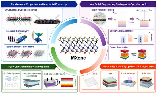
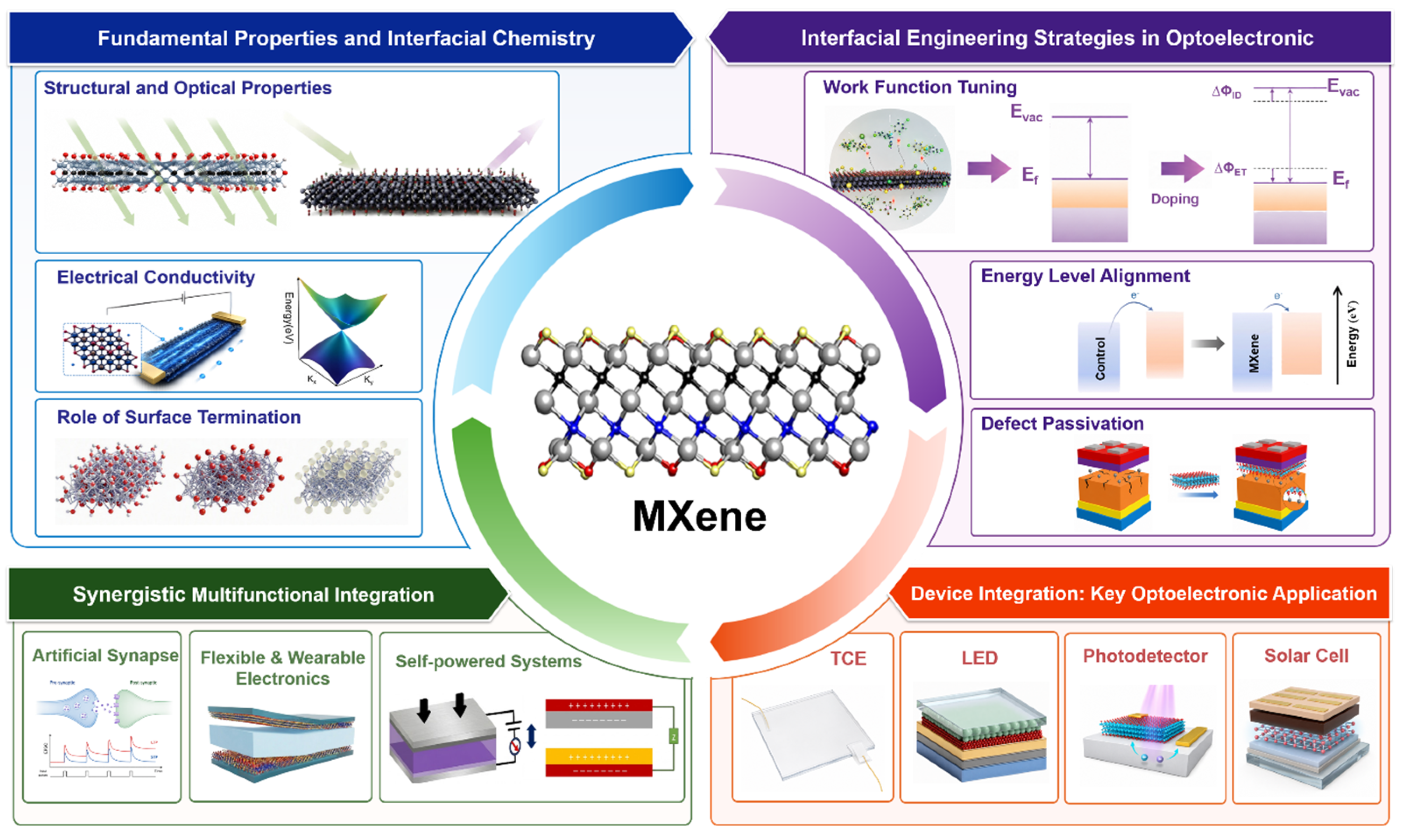
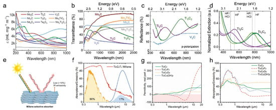
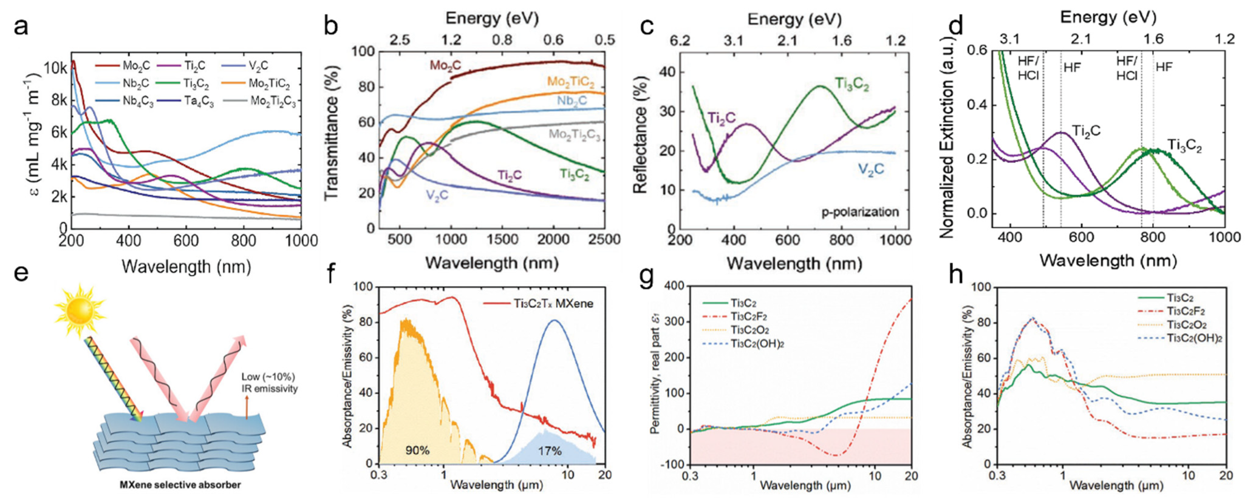
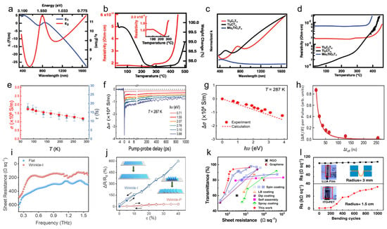
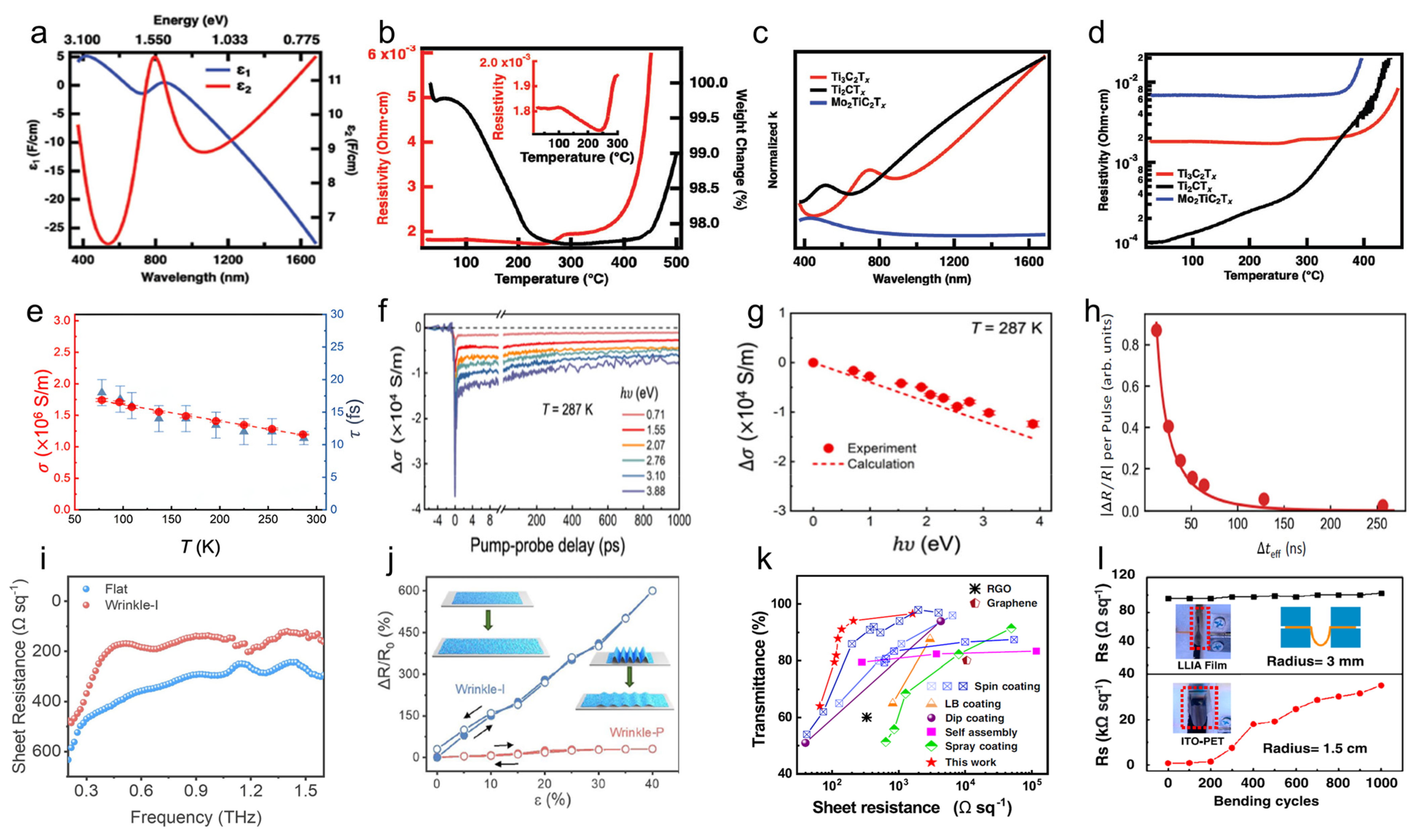
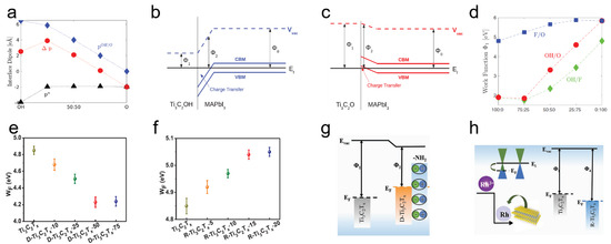
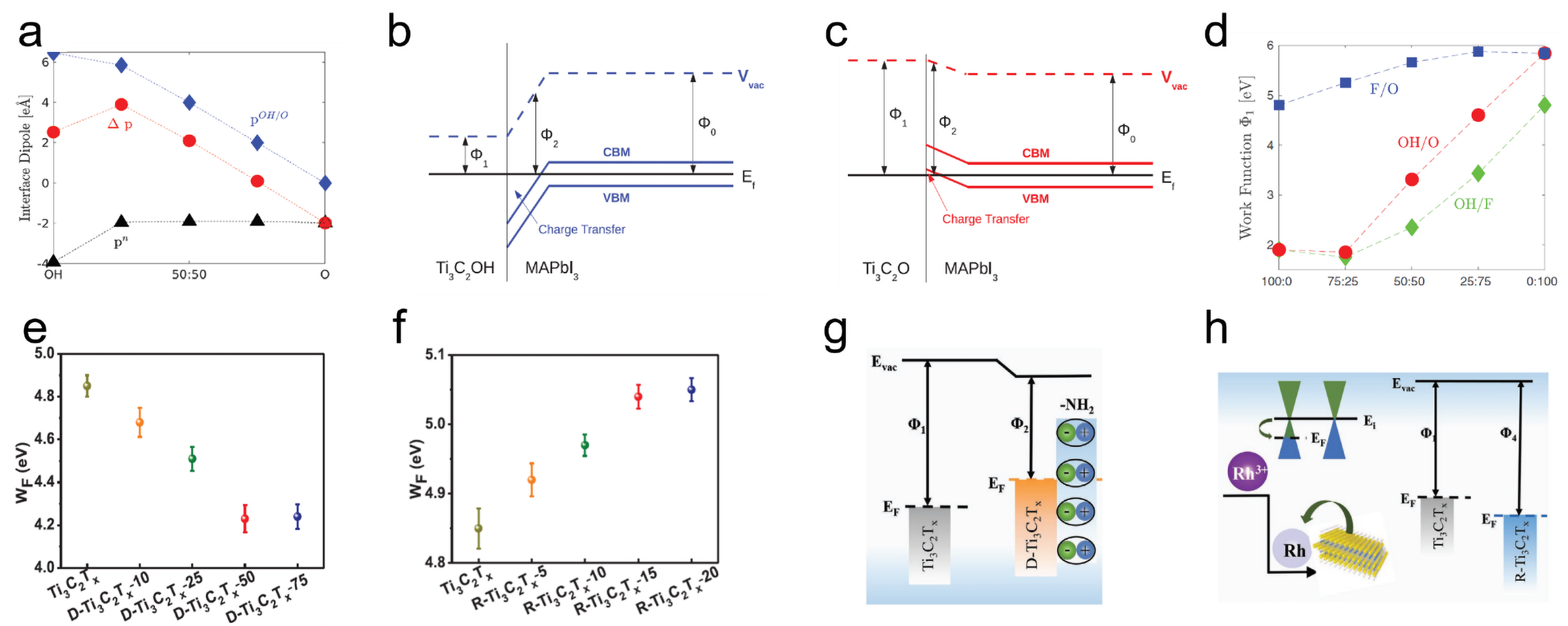
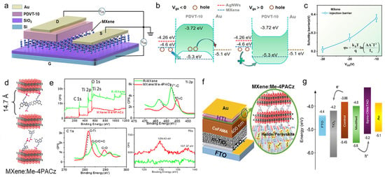
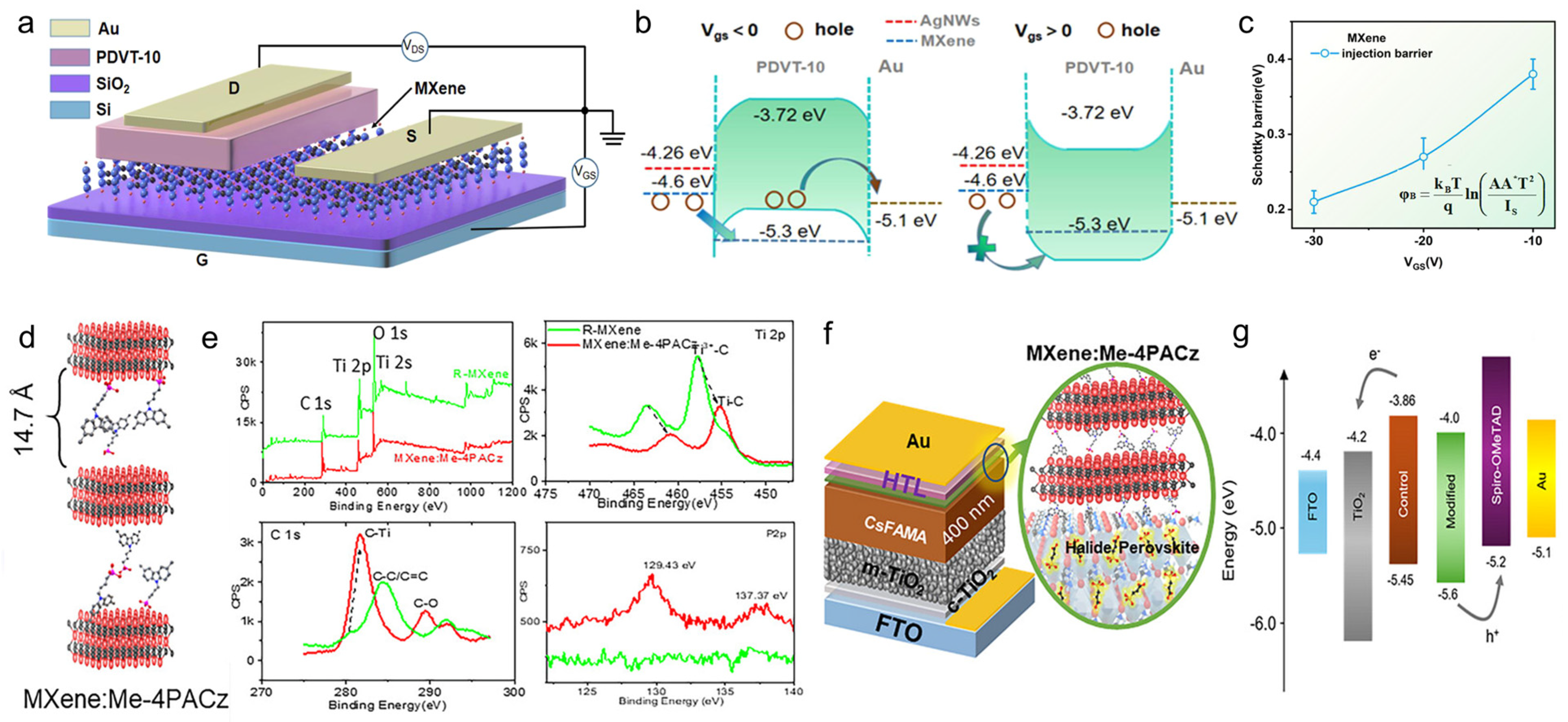
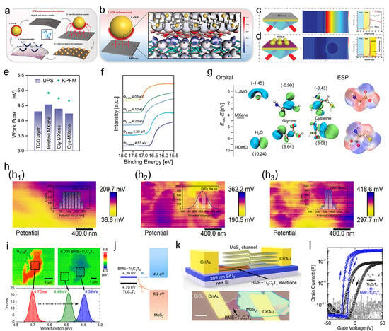
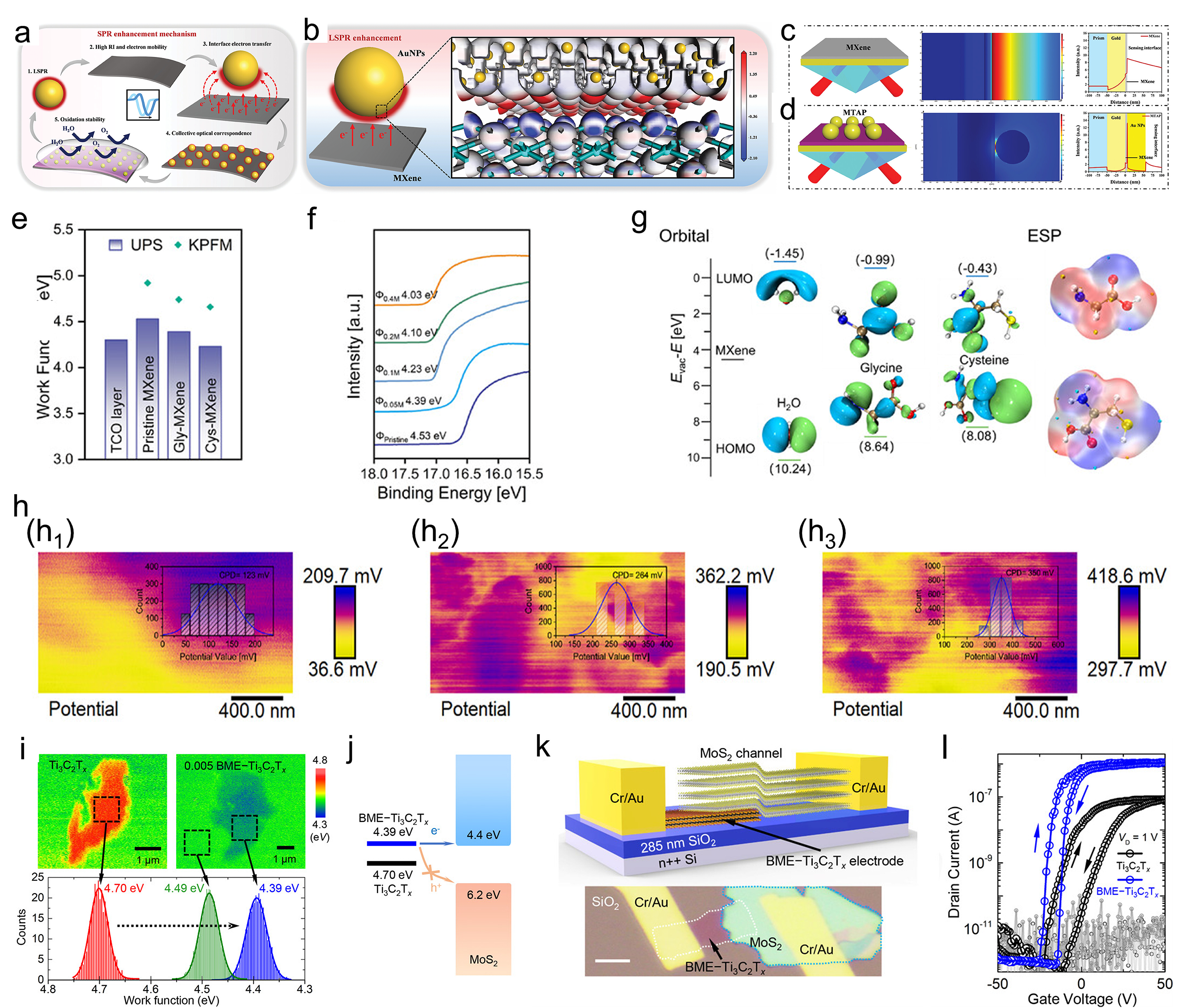


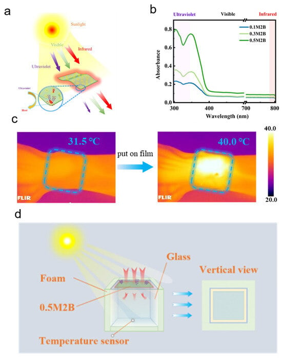
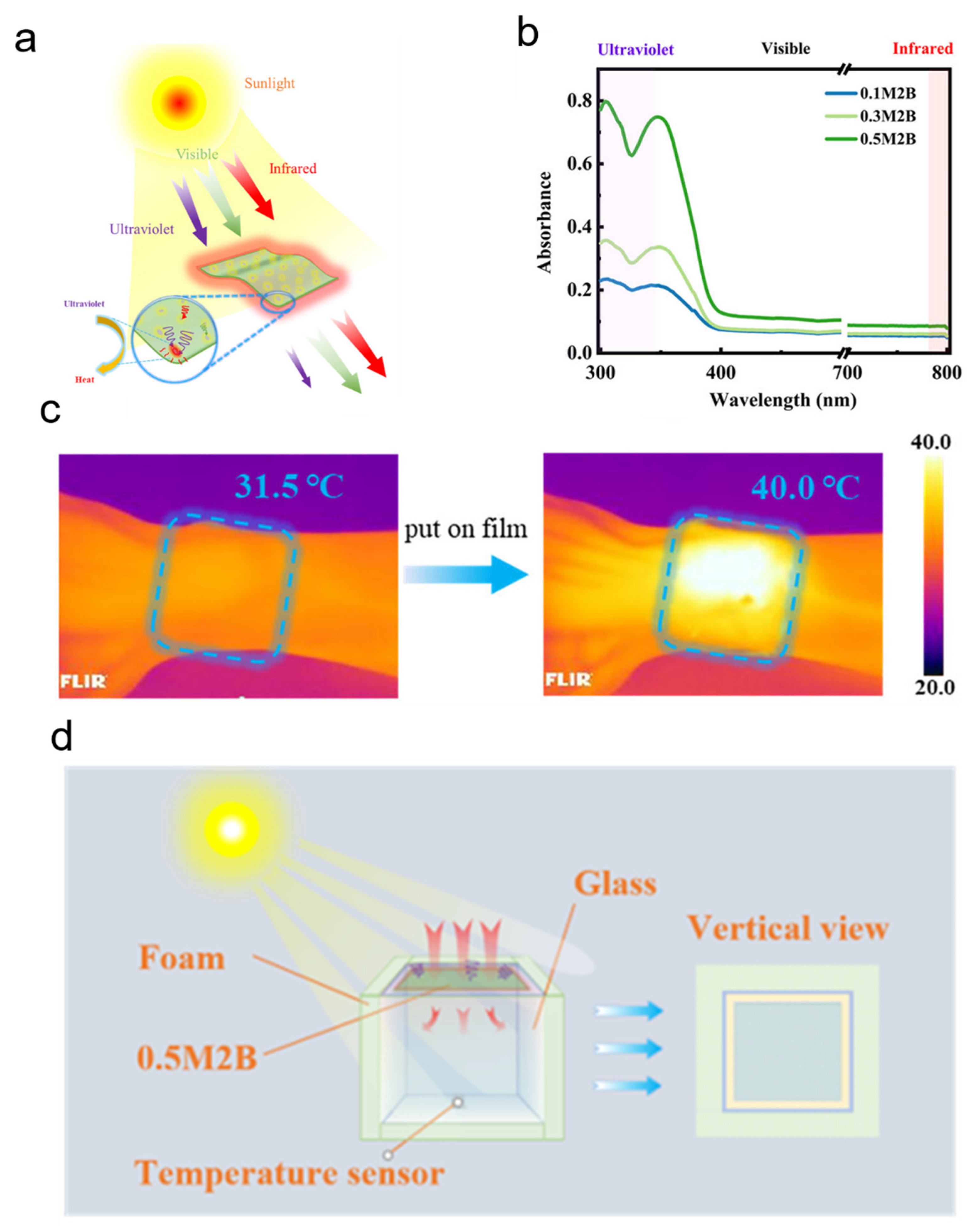
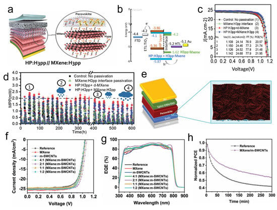
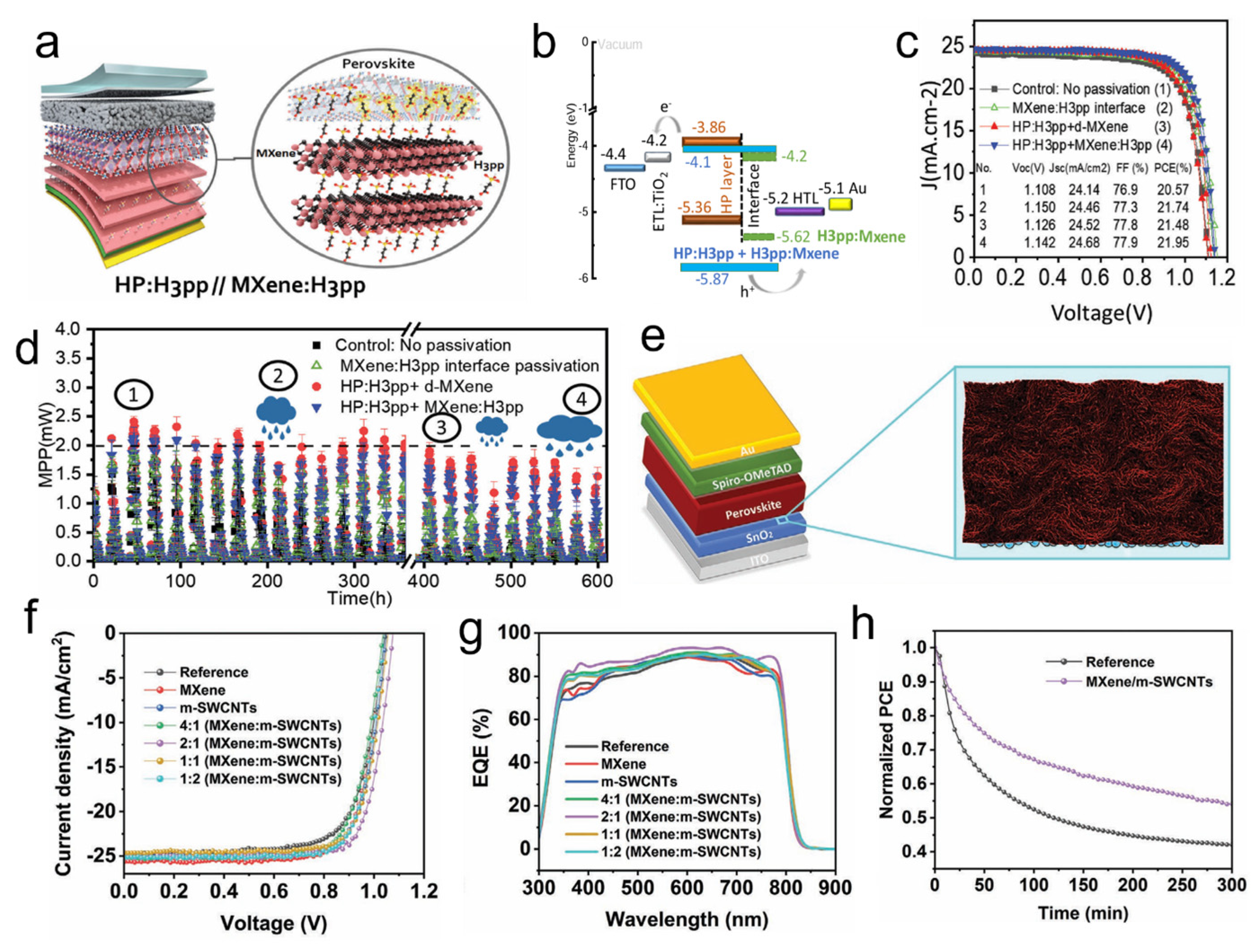
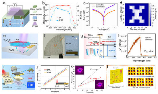
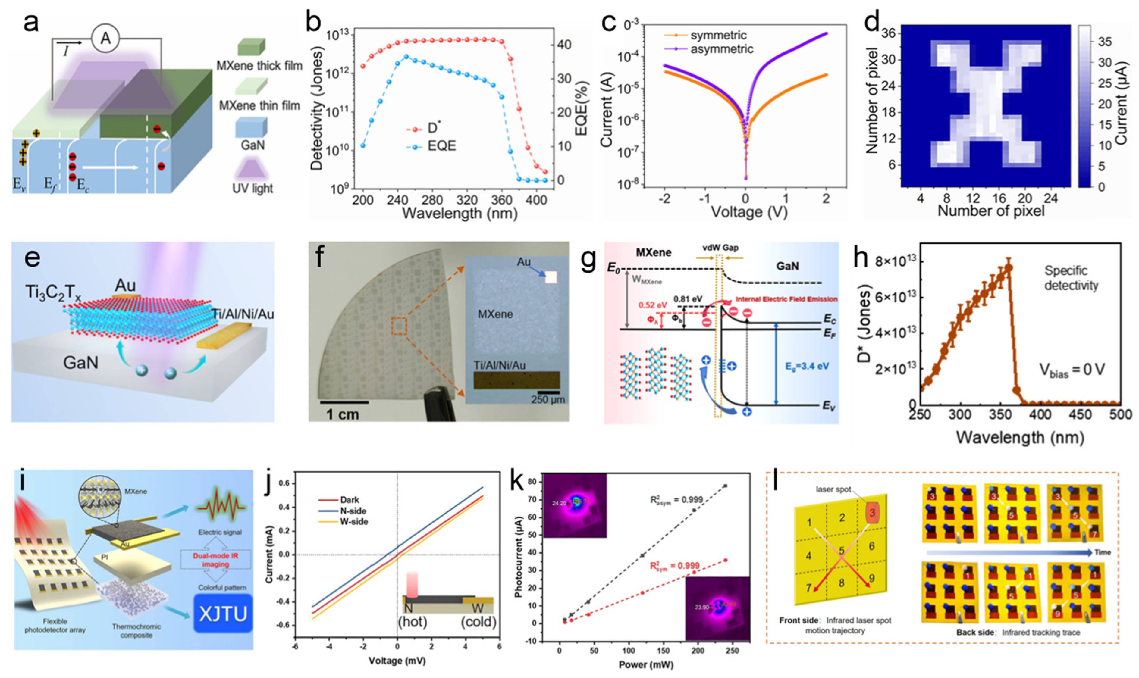
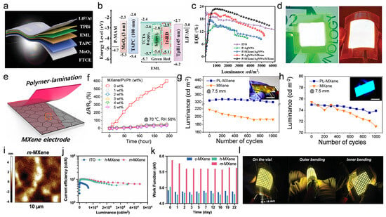
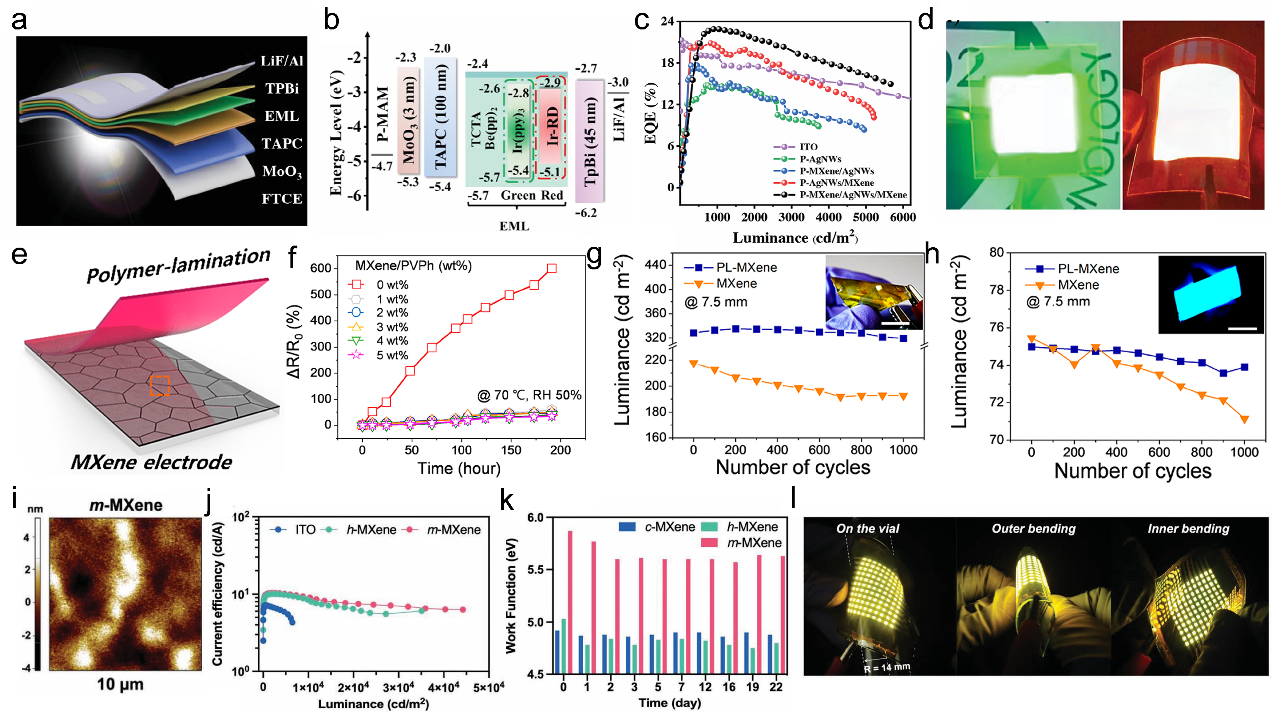
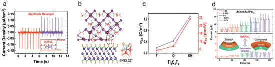
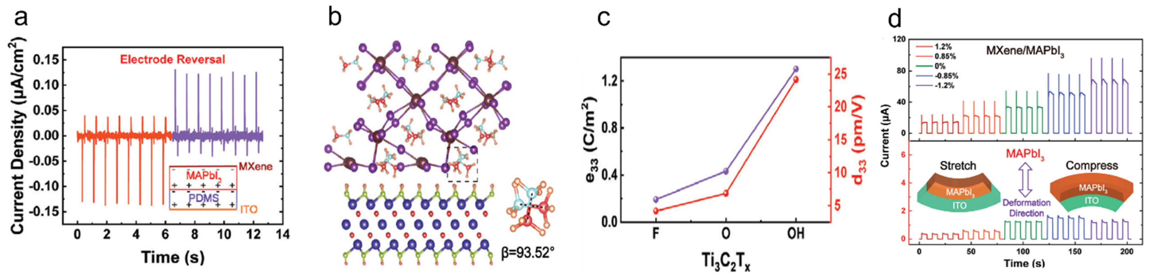
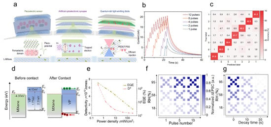
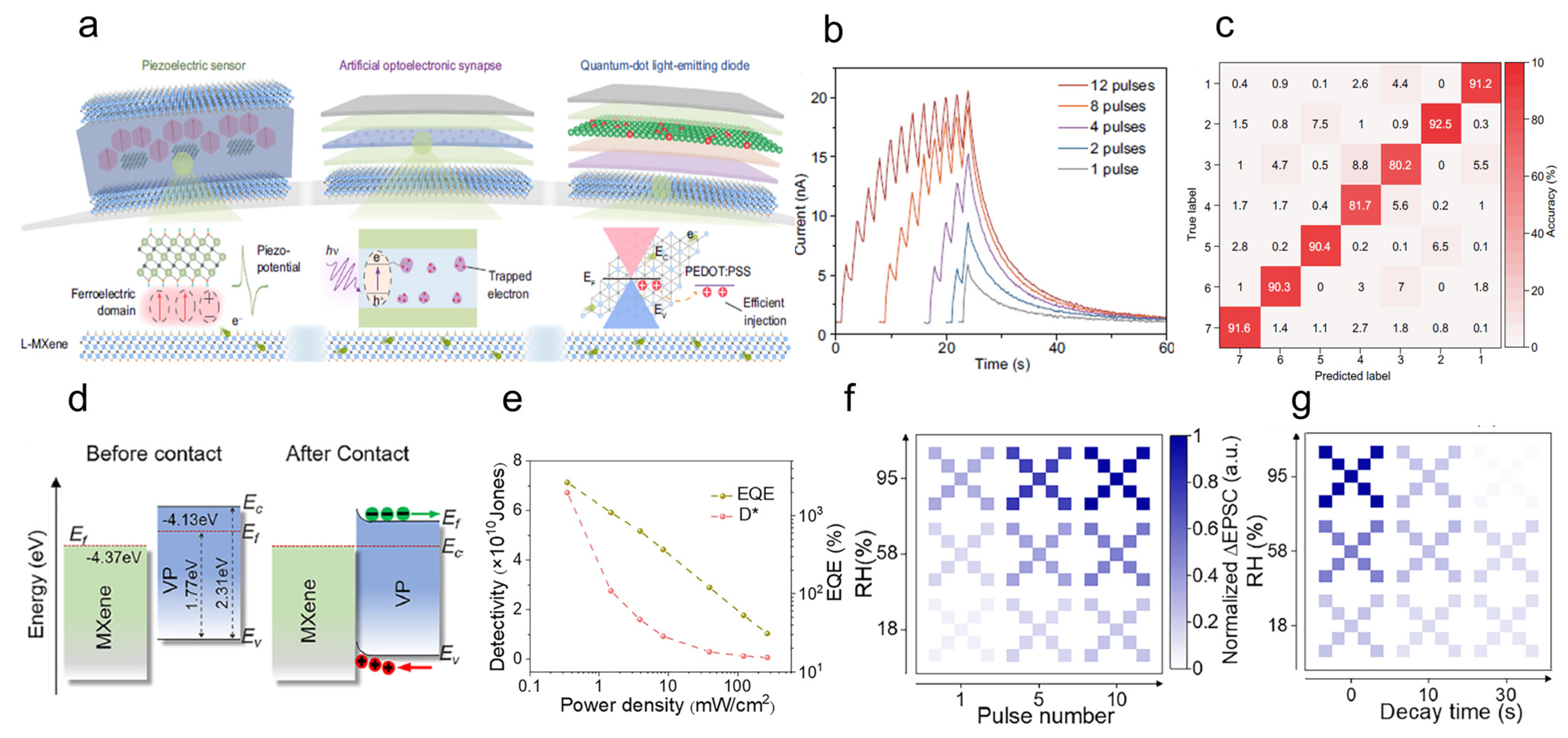

Disclaimer/Publisher’s Note: The statements, opinions and data contained in all publications are solely those of the individual author(s) and contributor(s) and not of MDPI and/or the editor(s). MDPI and/or the editor(s) disclaim responsibility for any injury to people or property resulting from any ideas, methods, instructions or products referred to in the content. |
© 2026 by the authors. Licensee MDPI, Basel, Switzerland. This article is an open access article distributed under the terms and conditions of the Creative Commons Attribution (CC BY) license.