


Abstract
A double-staggered grating waveguide slow wave structure (DSGW–SWS) is designed for a 340 GHz traveling wave tube (TWT). Input and output couplers were also designed to isolate the electron beam source from the electromagnetic (EM) signal. Transition sections in the SWS circuits were made by tapering the height of the DSWG to improve the matching of the circuit with the couplers. The reflection coefficient has a wide range from 326 GHz to 364 GHz below −15 dB. Particle-in-cell (PIC) simulation is performed using an ideal particle source for sheet electron beam (SEB), considering the filling factor to be around 50%. The average input power of a 340 GHz signal is said to be 0.19 W, which is amplified to 17.4 W with a gain of 19.55 dB.
1. Introduction
Vacuum electronic devices (VEDs) constitute the most remarkable high-power oscillators and amplifiers at the Terahertz frequency domain [1,2,3,4]. One of the significant VEDs is a traveling wave tube (TWT), which holds a broad range of applications in commercial and military sectors because of its large bandwidth and high power at high frequencies. An important part of a traveling wave tube is the slow wave structure (SWS) for beam–wave interaction. Optimizing the SWS to increase the interaction impedance and reduce the phase velocity of the wave results in better beam–wave interaction, hence increasing the output power of the TWT. Commonly used slow wave structures include double-staggered grating waveguides [5,6,7], sine waveguides [8,9] and folded waveguides [10,11,12].
In terms of operational bandwidth, the double-staggered grating waveguide (DSGW) has an advantage over the folded waveguides and sine waveguides. In a previous study [13], an optimized 220 GHz double-staggered grating waveguide (DSGW) amplifier produced 67 W of output power with a 3 dB bandwidth of 31.5 GHz, operating at a 25 kV beam voltage and 80 mA beam current. A 200 GHz DSGW operating at 20 kV and 100 mA was reported in Ref. [14]. A peak gain achieved with a 40 mm long tube was 18.9 dB. In Ref. [10] a staggered double-segment grating SWS achieves 32.8 W at 340 GHz with a 19.2 kV, 60 mA beam. Nevertheless, its intricate three-dimensional geometry is difficult to fabricate, especially when contrasted with the simpler planar alternative presented here in the article. In Ref. [15], a 0.34 THz traveling wave tube is discussed with an output power of 25 W and a gain of 40 dB but having a shorter bandwidth of 10 GHz. A folded waveguide TWT having an output power of 3.1 W at 336.96 GHz and a corresponding gain of 26.2 dB is reported in Ref. [16]. The amplification is achieved by the interaction of a cylindrical electron beam of 16.2 kV and 25.2 mA with an RF signal of 7.2 mW.
In this article we will discuss the design of a staggered double grating slow wave structure and H-plane 90-degree bend input–output couplers with Bragg reflectors for a 340 GHz traveling wave tube amplifier. The description of the SDG-SWS unit cell and its electromagnetic properties are discussed in Section 2. In Section 3 the transmission characteristics of the SWS and the coupler are discussed. The beam–wave interaction is studied using the computer simulation technology particle-in-cell (CST-PIC) solver, and the results are presented in Section 4. The conclusion and some results are discussed in Section 5.
2. Unit Cell and Electromagnetic Properties
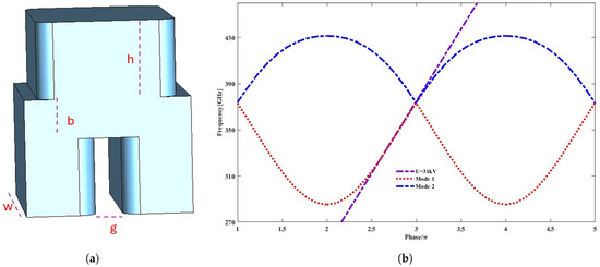
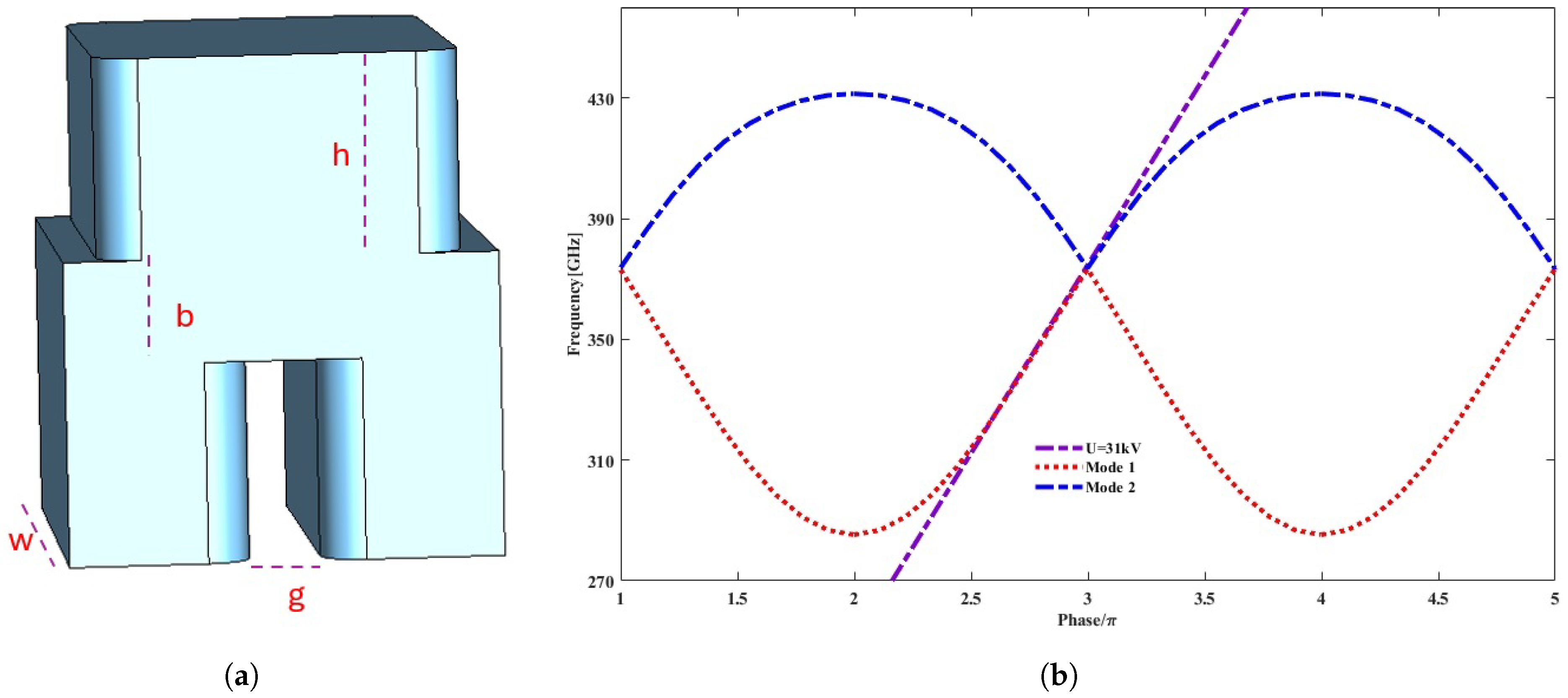
The unit cell of a staggered double grating slow wave structure is shown in Figure 1a. The optimized parameters of the unit cell are given in Table 1. The CST studio eigenmode solver is used to optimize the unit cell parameters and to achieve a linear dispersion curve. Figure 1b shows the dispersion curve of the unit cell with two fundamental modes. To obtain the operating frequency of each mode, the axial phase shift in each cell is swept from to 5 in eigenmode simulation. It can be seen that the beam voltage line of 31 kV matches with dispersion curves of both mode 1 (forward wave) and mode 2 (backward wave) for a wide frequency range of 319 GHz to 373 GHz and 373 GHz to 397 GHz, respectively, making it eligible for dual-mode operation.
Figure 1.
(a) Unit cell of SDGW. (b) Dispersion curve.
Table 1.
Dimensional values of SWS unit cells.
Another important figure of merit in the design of a TWT–SWS is the interaction impedance expressed as
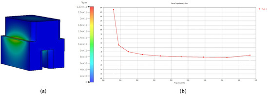
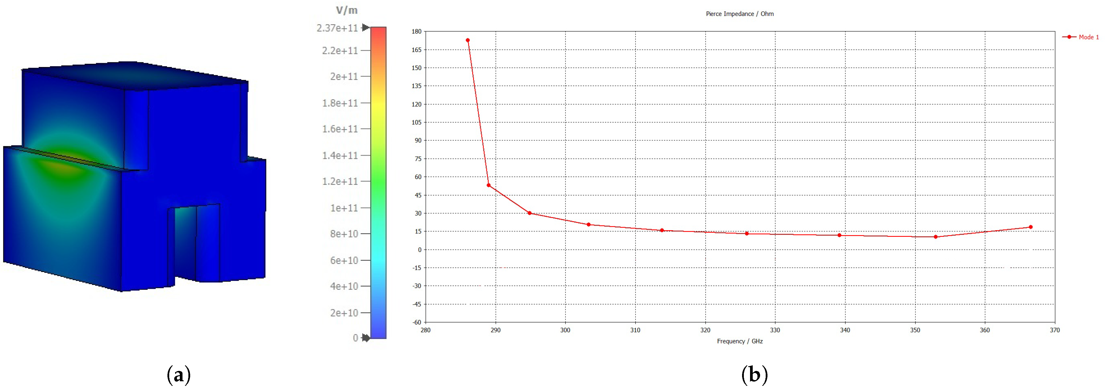
It gauges the coupling strength between the waveguide mode and the electron beam. The interaction impedance is a quantifier of how effectively an electron beam interacts with the axial component of the propagating electromagnetic wave. Therefore, the higher the interaction impedance, the higher the energy transfer from the electron beam. Figure 2 shows the longitudinal electric field intensity and the interaction impedance of the TM11-like mode.
Figure 2.
(a) Longitudinal electric field of Mode 1. (b) Interaction impedance.
3. Transmission Analysis of SWS
The slow wave structure comprises 100 optimized unit cells repeated along the axial direction (z-axis). In the DSG slow wave structures, the electromagnetic power cannot be decoupled from the beam under normal interaction conditions. Hence, designing an efficient coupling structure is critical. The power can be taken out of the tube either in a vertical or horizontal direction with respect to the beam plane. Therefore, 90-degree bend H-plan input–output couplers are used for this purpose. Bragg reflectors at the ends of the couplers are there to avoid the loss of RF signal into the electron gun.
Ohmic losses from surface roughness are modeled via the Hammerstad–Bekkadal formula expressed in Equation (1) to accurately predict frequency-dependent bulk conductivity under realistic conditions.
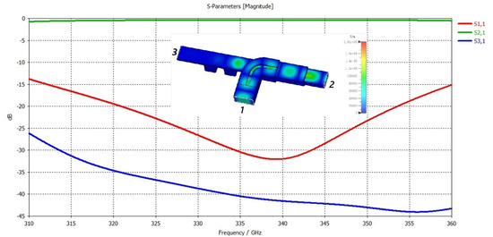
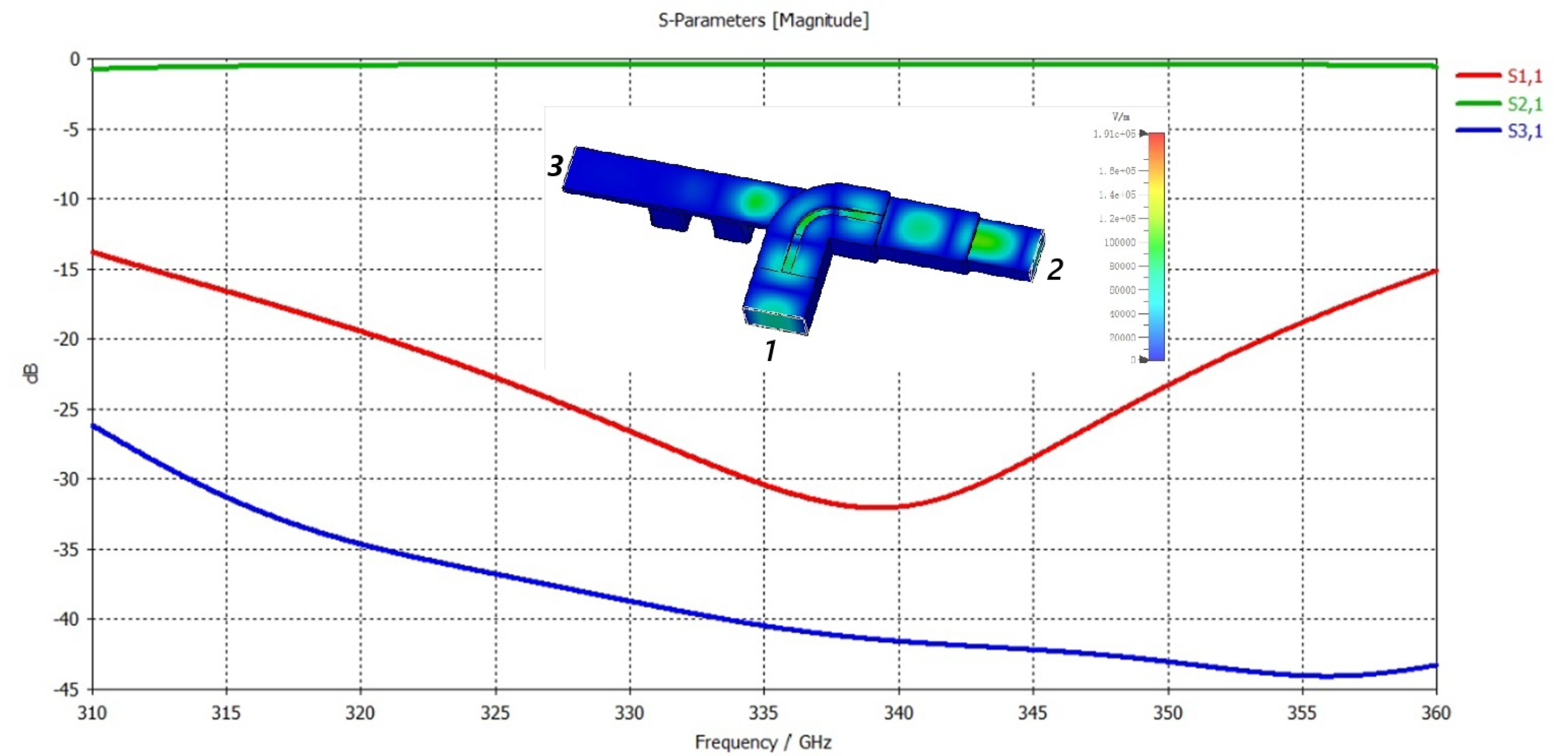
where is vacuum conductivity, h is the surface roughness of the material and is the skin depth. If the roughness of the copper is 300 nm at 340 GHZ, the conductivity is calculated to be 1.53 × 10² S/m. Considering these values, the time-domain solver simulation of the coupler is performed to find the s-parameters. Figure 3 shows that the reflection loss is less than −15 dB and the is greater than −1 dB for a frequency ranging from 311 GHz to 360 GHz, making the coupler well eligible to be used in the circuit.
Figure 3.
Electric field and s-parameters of coupler.
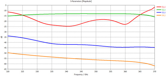
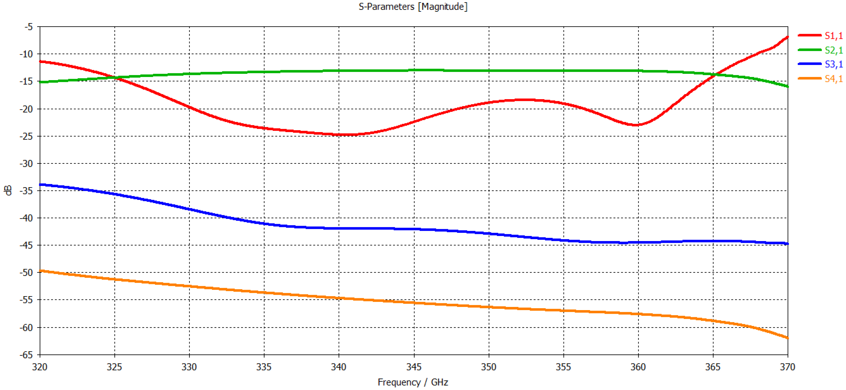
The three unit cells at both the input and output sides of the circuit are tapered to make a transition section, which optimizes SWS-to-coupler impedance matching at both ends. Hence, improving the transmission characteristics of the SWS by reducing mismatch losses. The total length of the SWS, including the transition section, is 40 mm. Results of the time-domain solver simulation considering the above-mentioned roughness and conductivity are shown in Figure 4. The design achieved a good impedance matching with below −15 dB from 326 GHz to 364 GHz, making an operational bandwidth of 38 GHz.
Figure 4.
S-parameters of the SWS circuit along with the input and output coupler.
4. Beam–Wave Interaction
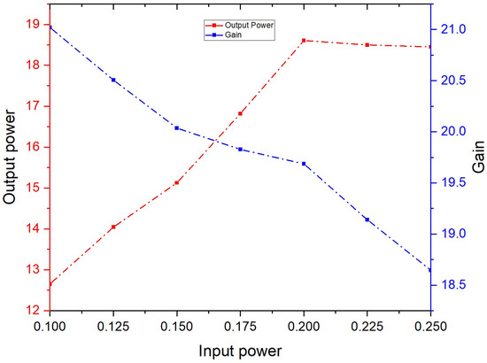
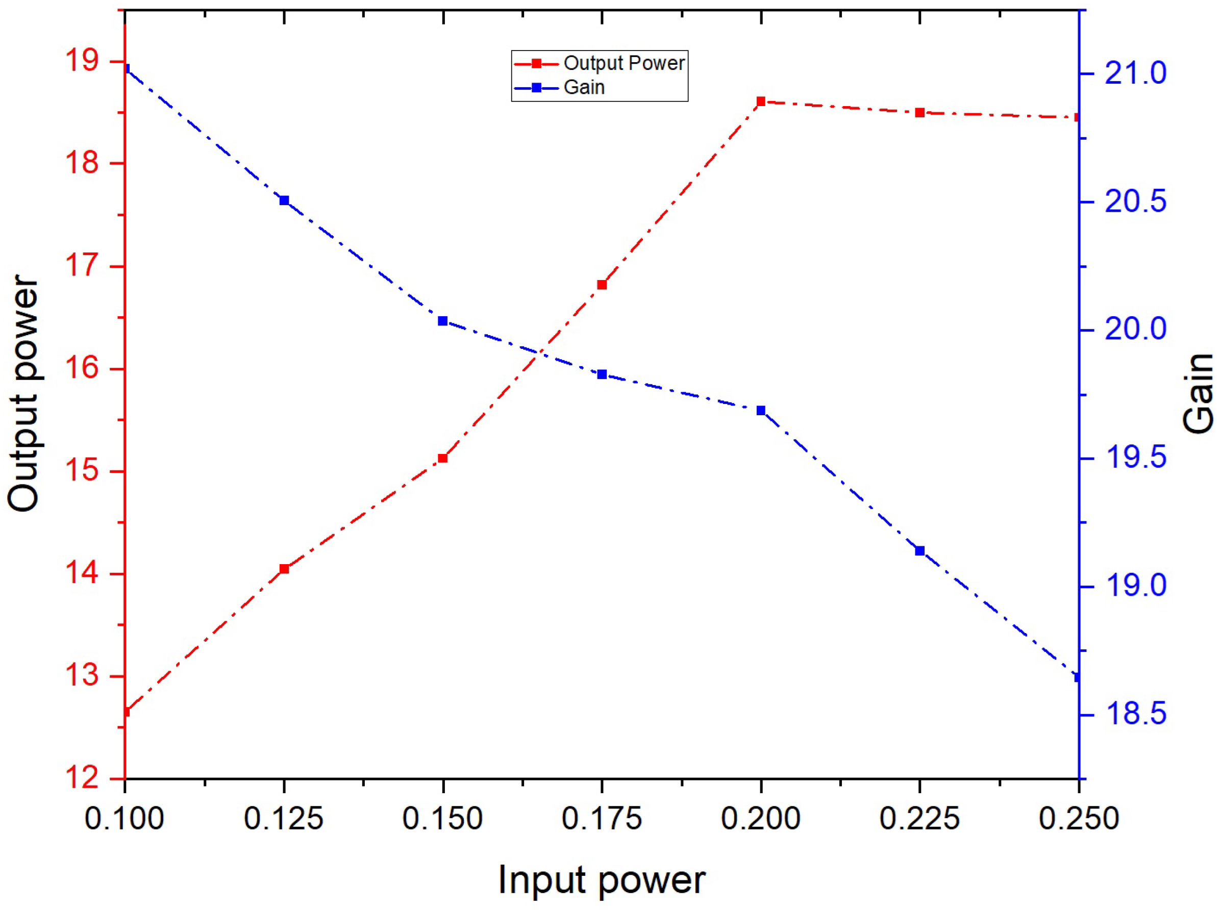
The CST particle studio is used for PIC simulation for evaluating the hottest characteristics of the above-discussed SWS in a TWT. This simulation considers the overall circuit consisting of the SWS and the input–output couplers. The cross-section size of the particle source used is 0.48 × 0.052 mm2. The beam used has a current of 40 mA and a voltage of 31 kV. An analytic magnetic field with an axial component of 0.6 T is used to confine the beam. The small signal gain of the circuit is kept near 20 dB to avoid oscillations. Particle-in-cell simulation is performed for an input signal of frequency 340 GHz with different input power levels. The length of the circuit is kept constant with 100 periods of SWS unit cells as considered for the transmission analysis in the above section. In Figure 5, a graph between input power, output power and gain is shown. A saturated average power of 18.6 W and a gain of 19.6 dB is achieved for the input signal of 0.21 W, as depicted from the graph.
Figure 5.
Input power vs. output power and gain.
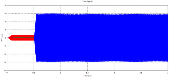
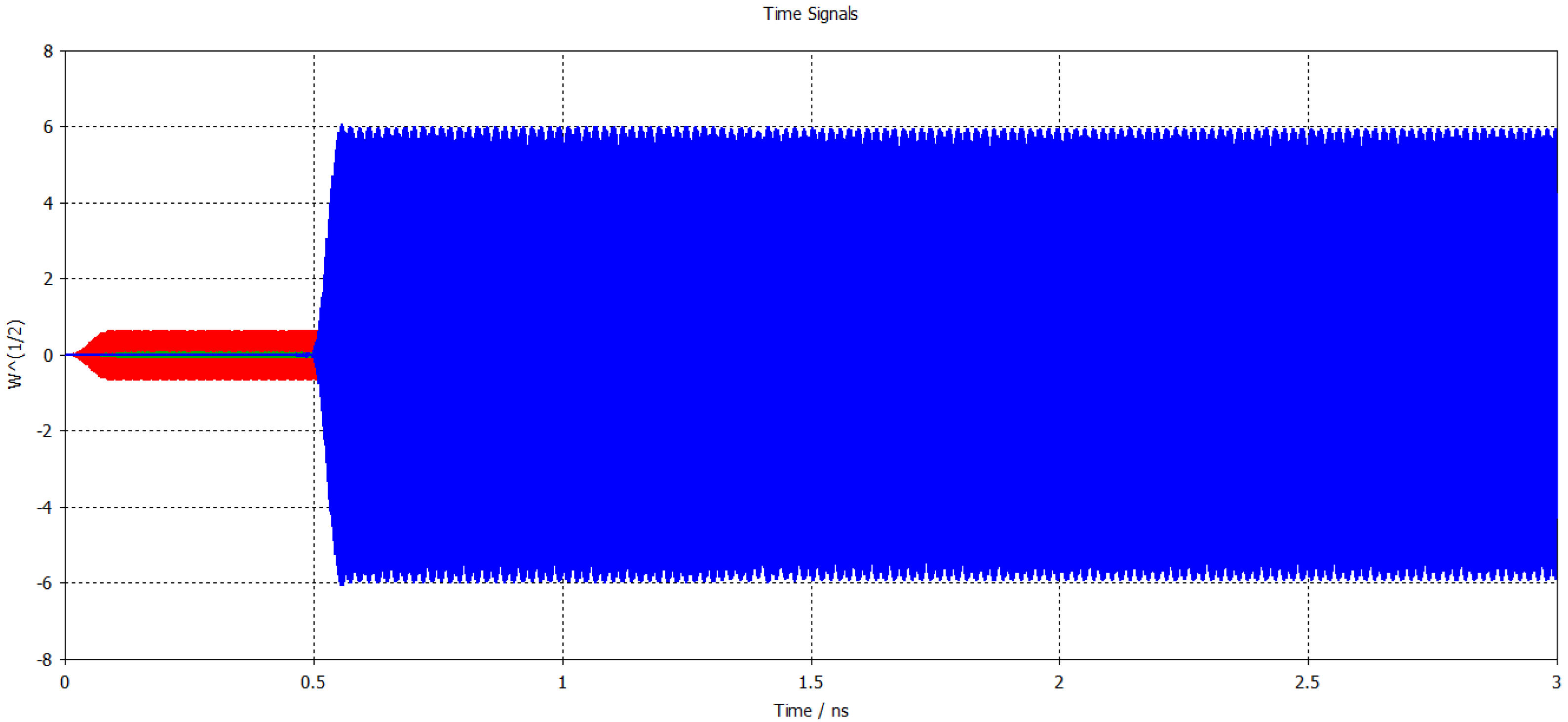
Considering the saturation condition from the above graph and to avoid the oscillations, a time domain simulation with the average input power of 0.19 W was performed. The result of this simulation is shown in Figure 6, where the output amplified signal with a peak power of 5.8 W can be seen. It is depicted that the output signal becomes stable at 0.55 ns, generating an average output power of 17.4 W. Based on this result, the gain of the circuit is calculated to be 19.55 dB.
Figure 6.
Input–output signal versus time at 340 GHz.
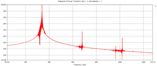
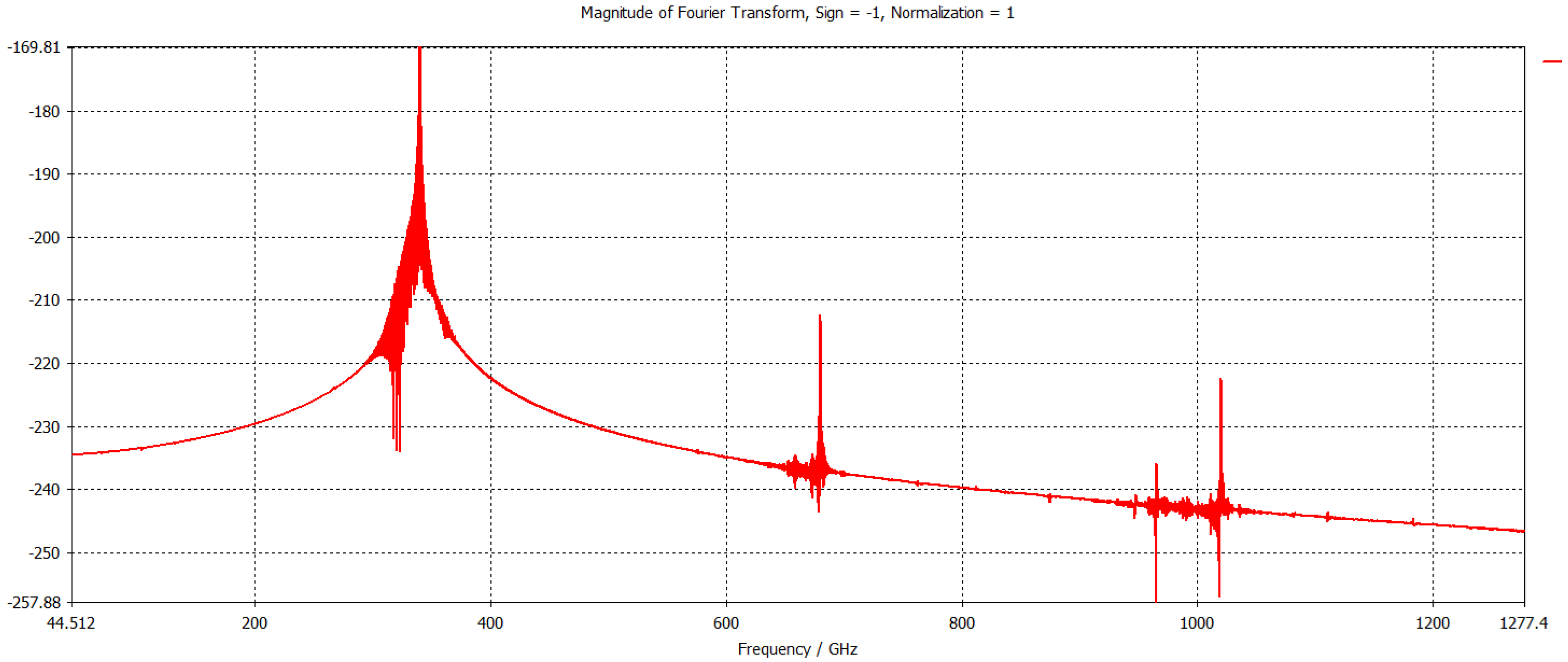
The frequency spectrum of the output signal is illustrated in Figure 7, showing a stable spectrum concentrated at frequency 340 GHz. The normalized amplitude at the other frequency points is quite minimal, which shows that the competing modes are well suppressed.
Figure 7.
Fourier spectrum of the output signal.
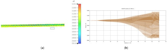
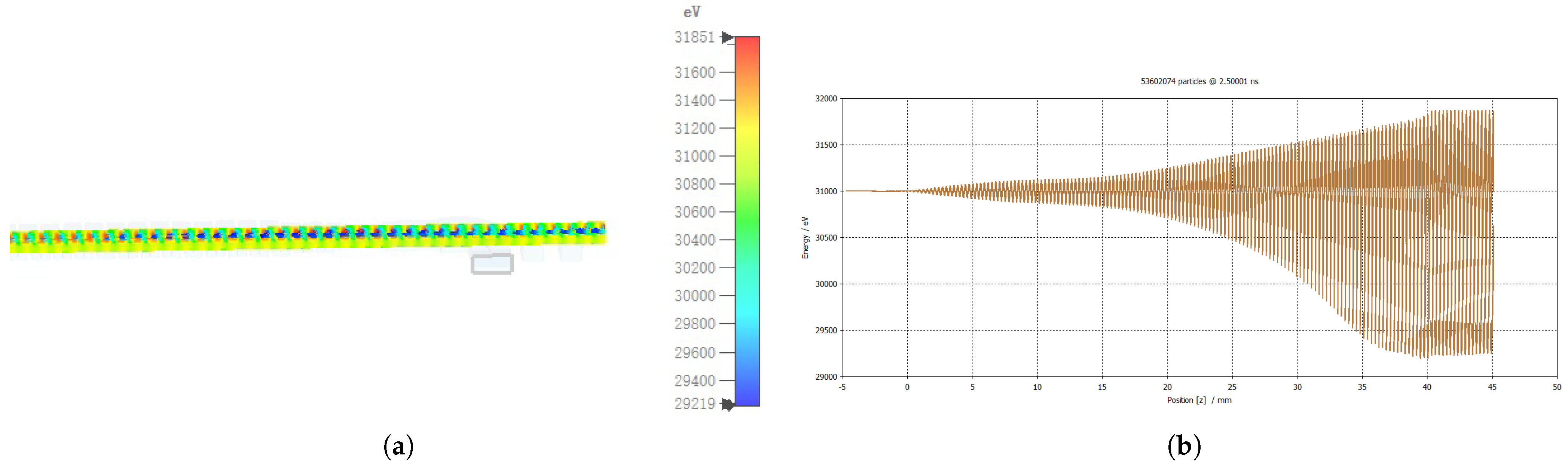
Longitudinal bunching within the tube, shown in Figure 8a, arises from velocity modulation of the electron beam due to its interaction with the input signal’s electromagnetic field. The accompanying longitudinal energy distribution provides additional evidence of this process. Figure 8b clearly demonstrates electron deceleration toward the tube’s end, indicating energy transfer from the beam to the EM wave and resulting in signal amplification.
Figure 8.
(a) Bunching effect; (b) energy vs. phase graph.
5. Conclusions
The design of a double-staggered grating waveguide for a 340 GHz frequency signal is discussed in this paper. The SWS has been designed by optimizing the unit cell to achieve better interaction impedance. Input and output couplers are also designed as a part of the circuit to isolate the electron beam from the high-frequency circuit. The transmission characteristics show a good passband of 38 GHz for the DSGW. The hottest characteristics of the tube are also studied to analyze the beam–wave interaction in detail.
Author Contributions
M.H.J. led the study’s conceptualization and directed the overall planning and execution of the project. He also drafted the initial version of the manuscript and played a major role in the revisions. N.S.A. contributed to simulations and data visualization, preparing all figures and tables. H.S. provided his support during the execution and error correction of the project. W.H. provided supervision and offered critical insights and guidance throughout the research. All authors reviewed the manuscript, provided constructive feedback, and approved the final version for submission. All authors have read and agreed to the published version of the manuscript.
Funding
This research received no external funding.
Institutional Review Board Statement
Not applicable.
Informed Consent Statement
Not applicable.
Data Availability Statement
The data that support the findings of this study are available from the corresponding author upon reasonable request.
Acknowledgments
We would like to express our sincere gratitude to Wenlong He for their invaluable guidance and support throughout this research.
Conflicts of Interest
The authors declare no conflicts of interest.
References
- Shu, G.; Pan, H.; Li, Q.; Xie, X.; Ma, S.; Tang, J.; Liu, S.; Li, M.; Yin, H.; Ruan, C.; et al. Cosimulation and Cold Test Verification of a 220-GHz Sheet Beam Traveling-Wave Tube Amplifier. IEEE Trans. Electron Devices 2024, 71, 1253–1260. [Google Scholar] [CrossRef] [Scilit]
- Jamil, M.H.; Lin, Z.; Sharif, H.; Abbas, N.S.; He, W. Design and Simulation of an Electron Optical System for Terahertz Vacuum Devices. Micromachines 2015, 16, 928. [Google Scholar] [CrossRef] [Scilit] [PubMed]
- Sharif, H.; Jamil, M.H.; He, W.; Abbas, N.S. Design of Quasi-Optical TE17,6 Mode Converter for High-Power 170-GHz Gyrotrons. IEEE Trans. Plasma Sci. 2025, 53, 834–841. [Google Scholar] [CrossRef] [Scilit]
- Feigin, L.; Gover, A.; Minnes, R.; Nause, A. Tapering enhanced superradiance with a planar magnetic undulator. Phys. Rev. Accel. Beams 2025, 28, 110702. [Google Scholar] [CrossRef]
- Shin, Y.-M.; Barnett, L.R.; Luhmann, N.C. Phase-Shifted Traveling-Wave-Tube Circuit for Ultrawideband High-Power Submillimeter-Wave Generation. IEEE Trans. Electron Devices 2009, 56, 706–712. [Google Scholar] [CrossRef] [Scilit]
- Babaeihaselghobi, A.; Akram, M.N.; Ghavifekr, H.B.; Billa, L.R. A Novel Chevron-Shape Double-Staggered Grating Waveguide Slow Wave Structure for Terahertz Traveling Wave Tubes. IEEE Trans. Electron Devices 2020, 67, 3781–3787. [Google Scholar] [CrossRef] [Scilit]
- Shu, G.; Li, Q.; Xie, X.; Lin, J.; Lin, G.; Liao, J.; Pan, H.; He, W. Study of a 0.3 THz Double-Staggered Grating Waveguide-Based Band-Edge Oscillator. IEEE Trans. Plasma Sci. 2024, 52, 5151–5158. [Google Scholar] [CrossRef] [Scilit]
- Zhang, L.; Ma, G.; Jiang, Y.; Lei, W.; Hu, P.; Tang, X.; Chen, H.; Wei, Y. Demonstration of a Double Flat-Roofed Sine Waveguide Slow Wave Structure with Low Loss for 220-GHz Traveling-Wave Tube. IEEE Microw. Wirel. Technol. Lett. 2023, 33, 291–294. [Google Scholar] [CrossRef] [Scilit]
- Nayek, S.N.; Sonkar, R.K.; Tiwari, T.; Bhattacharjee, R. Design and Analysis of Truncated Velocity Tapered Sine-Waveguide Structure for Traveling-Wave Tube in THz Band. IEEE Trans. Plasma Sci. 2022, 50, 4759–4766. [Google Scholar] [CrossRef] [Scilit]
- Wang, Z.; Zhu, J.; Lu, Z.; Duan, J.; Chen, H.; Wang, S.; Wang, Z.; Gong, H.; Gong, Y. A Novel Staggered Double-Segmented Grating Slow-Wave Structure for 340 GHz Traveling-Wave Tube. Sensors 2023, 23, 4762. [Google Scholar] [CrossRef] [Scilit] [PubMed]
- Feng, Y.; Pan, P.; Zhang, C.; Tian, H.; Feng, J. A Novel Design of G-Band Broadband Low-Gain Fluctuation Slow-Wave Structure with Improved Folded Waveguides. IEEE Trans. Electron Devices 2023, 70, 2767–2772. [Google Scholar] [CrossRef] [Scilit]
- Xu, D.; Wang, S.; Wang, Z.; Shao, W.; He, T.; Wang, H.; Tang, T.; Gong, H.; Lu, Z.; Duan, Z.; et al. Theory and Experiment of High-Gain Modified Angular Log-Periodic Folded Waveguide Slow Wave Structure. IEEE Electron Device Lett. 2020, 41, 1237–1240. [Google Scholar] [CrossRef] [Scilit]
- Shi, X.; Wang, Z.; Tang, X.; Tang, T.; Gong, H.; Zhou, Q.; Bo, W.; Zhang, Y.; Duan, Z.; Wei, Y.; et al. Study on Wideband Sheet Beam Traveling Wave Tube Based on Staggered Double Vane Slow Wave Structure. IEEE Trans. Plasma Sci. 2014, 42, 3996–4003. [Google Scholar] [CrossRef] [Scilit]
- Karetnikova, T.A.; Rozhnev, A.G.; Ryskin, N.M.; Fedotov, A.E.; Mishakin, S.V.; Ginzburg, N.S. Gain Analysis of a 0.2-THz Traveling-Wave Tube with Sheet Electron Beam and Staggered Grating Slow Wave Structure. IEEE Trans. Electron Devices 2018, 65, 2129–2134. [Google Scholar] [CrossRef] [Scilit]
- Guo, J.; Dong, Y.; Shi, N.; Wang, S.; Wang, Z.; Liu, X.; Tang, T.; Gong, H.; Lu, Z.; Duan, Z.; et al. A 0.34-THz Standing Wave Enhanced Sheet Electron Beam Traveling-Wave Tube. IEEE Trans. Electron Devices 2023, 70, 307–312. [Google Scholar] [CrossRef] [Scilit]
- Hu, P.; Lei, W.; Jiang, Y.; Huang, Y.; Song, R.; Chen, H.; Dong, Y. Demonstration of a Watt-Level Traveling Wave Tube Amplifier Operating Above 0.3 THz. IEEE Electron Device Lett. 2019, 40, 973–976. [Google Scholar] [CrossRef] [Scilit]

Disclaimer/Publisher’s Note: The statements, opinions and data contained in all publications are solely those of the individual author(s) and contributor(s) and not of MDPI and/or the editor(s). MDPI and/or the editor(s) disclaim responsibility for any injury to people or property resulting from any ideas, methods, instructions or products referred to in the content. |
© 2026 by the authors. Licensee MDPI, Basel, Switzerland. This article is an open access article distributed under the terms and conditions of the Creative Commons Attribution (CC BY) license.