


Abstract
Alkali atomic vapor cells are the key components of all kinds of atomic sensors, including atomic clocks, atomic gyroscopes, atomic magnetometers, Rydberg atom sensors, etc. With the miniaturization and integration trends of these atomic sensing devices, compact alkali vapor cells, particularly micromanufactured vapor cells with high performance, are urgently needed. The development history from glass vapor cells to MEMS vapor cells is reviewed. The bonding methods for macro-fabricated alkali atomic vapor cells, such as anodic bonding, metal film thermocompression bonding, glass–frit bonding, epoxy glue bonding and laser bonding, are analyzed and summarized. The alkali metal filling techniques for vapor cells are also discussed, including the physical methods of direct filling and wax package filling, and chemical methods of the reaction of alkali chloride with BaN6, ultraviolet (UV) light decomposition of RbN6 and CsN6, electrolysis of alkali-rich glass, and laser decomposition of alkali dispensers. Compared to traditional vapor cell dimensions, vapor cells with long laser paths are emphasized, and the corresponding design and realization processes are discussed. Finally, the vapor cells with inner anti-relaxation coatings and passivation coatings aimed at achieving long reaction times and long lifetimes are analyzed.
1. Introduction
Quantum sensors based on laser–atom interaction can accurately measure physical quantities, including frequency, angular velocity, magnetic field and electric field [1].
To date, frequency references based on laser–atom interactions have realized fractional uncertainties down to the range of 10−17–10−18 or even lower [2,3]. Magnetometers based on optical pumping are able to measure sensitive neuronal activity [4]. By designing a bi-planar coil system and combining it with a reference sensor array, the residual magnetic field of the magnetoencephalography in the subject’s head movement area is controlled to be within ±1 nT [5]. High-sensitivity terahertz electric field imaging is becoming a compelling atomic device. By collecting THz-induced optical fluorescence and using atomic properties for the calibration of field strength, a real-time THz standing wave image is demonstrated [6].
With the appropriate design of optics and electronics, and with developing fabrication and assembly technologies, versatile atomic devices including atomic clocks [7,8,9,10], atomic magnetometers [11,12,13,14,15,16,17,18,19], atomic gyroscopes [20,21,22,23], and Rydberg atom sensors [24,25,26,27,28,29] have been investigated and realized. Some of the devices have already been commercialized and have numerous prospects [30]. Furthermore, the laser–atom reaction technologies are also used for some other novel devices, including laser spectrometers [31], optical isolators [32], magneto-optic traps [33], optical interfaces [34], photonic crystals [35,36], and some cutting-edge physics experiments, including systematic effect analysis in gas spin comagnetometers [37], searching for topological defect dark matter [38], constraints on exotic spin-velocity-dependent interactions [39], etc.
The vapor cells are the locations where stable atomic reference transitions are provided. They hermetically isolate the alkali metals from the surroundings while providing laser transparency. For atomic clocks and magnetometers, buffer gases are also added to the cells along with the alkali atoms. The intentional addition of a buffer gas reduces wall-induced collisional decoherence of the atoms as well as the Doppler broadening effects so as to improve the transition quality factors [40].
As the most important parts of atomic sensing devices, alkali vapor cells have an obvious influence on the performance of the devices. The geometry of the cell contributes to determining important device parameters, such as beam size and orientation [41], optical path length [42], the alkali atom–wall collision rate [43,44], etc.
Traditional vapor cells are fabricated via the glass-blowing technique [45,46]. This process can easily produce discrete vapor cells with moderate volume and high hermeticity.
With the miniaturization and integration trends of atomic sensors, alkali vapor cells are required to be miniaturized accordingly because their dimensions directly limit the final size of the entire sensing device. Studies have been carried out to miniaturize the glass-blowing alkali vapor cells [47,48], but it is still difficult to integrate MEMS technology into the glass vapor cell process to realize wafer-scale fabrication of atomic sensing devices.
In recent years, MEMS atomic vapor cells have received increasing attention due to their compatibility with integrated circuit (IC) technology and ease of miniaturization. Compared with glass vapor cells, they have the advantages of high uniformity and batch manufacturing, making them more suitable for applications in developing chip-scale atomic sensing devices.
The main purpose of this study is to systematically review the fabrication technologies of miniaturized atomic vapor cells, including glass cells but mainly MEMS cells. The technologies include wafer bonding methods, alkali metal packaging methods, cell inner coating technologies, etc., with a detailed discussion on their strengths and weaknesses. Based on these technologies, vapor cells with different structures for different application scenarios can be realized.
2. Classifications
2.1. Glass Vapor Cells
Alkali metal vapor cells based on glass-blowing techniques are the first type of vapor cells applied in atomic sensors. This unique and versatile method for vapor cell fabrication is illustrated in Figure 1.
Figure 1.
Methods for filling glass-blowing alkali vapor cells.
A batch of empty glass cells are connected to a manifold through thin glass capillaries. The manifold provides access to alkali metal sources, a high-vacuum pump, buffer gas cylinders and, in some cases, a source of paraffin for vapor cell inner coating [49]. The whole system is first pumped down to a vacuum condition for alkali metal filling. The alkali metal, for example, rubidium, is usually produced through a chemical reaction process in which rubidium chloride and calcium are put together in a phial connected to the manifold and then heated to a temperature of about 400 °C. As a result, rubidium atoms are replaced by calcium and then diffuse as a vapor in the cell manifold. After the cells are filled with alkali metals and buffer gases, the fused sealing is achieved by heating the thin glass capillaries, and the cells are pinched off from the manifold [50].
With the developed glass-blowing technique, glass vapor cells with different shapes can now be readily fabricated, as shown in Figure 2.
Figure 2.
Different alkali vapor cells fabricated via glass blowing.
Because of the high-vacuum conditions and isolated sources, these centimeter-scale macroscopic vapor cells can meet stringent quality and purity specifications for alkali metals. Furthermore, glass-blowing cells can readily incorporate internal anti-relaxation coatings, which is beneficial for achieving superior performance [51].
Hollow-core glass fibers and laser heating sealing are used in conventional glass-blowing techniques so as to miniature the vapor cells. The use of thin glass fibers allows for very small cell size, and the highly localized laser heating of the glass has a negligible thermal effect on the adjacent alkali metal. Based on these related techniques, vapor cells with millimeter-scale or even smaller dimensions can be realized [52,53].
However, glass-blowing techniques present distinct drawbacks. Beyond the relatively large volume, vapor cells fabricated via this method typically feature a “cold finger”, which hinders integration with other miniature components. Additionally, individual cells have slight differences in shape, size, and buffer gas pressure, making it difficult to realize mass production with good consistency. Moreover, the cells must be fabricated one by one, making it really time-consuming for the production of large quantities.
Some alternative bonding techniques have been employed in vapor cell fabrications to overcome the limitations of the glass-blowing process, including epoxy glue bonding [54,55], glass fusion bonding [56], optical contact bonding [57], edge welding [58], hot wire cutting [59], and even glass–glass anodic bonding by using a thin silicon nitride interlayer [60].
More recently, the additive manufacturing approach and ultrafast laser welding have also been utilized to fabricate vapor cells. By using digital light processing technology, F. Wang et al. demonstrated a 3D-printed glass vapor cell. This vapor cell can be evacuated to a vacuum pressure of 2 × 10⁻⁹ mbar and filled with alkali vapor. The printed vapor cell exhibits high transparency and polarization stability, allowing for the observation of atomic spectroscopy [61].
Ultrafast laser welding technology has excellent localized thermal melting characteristics and holds broad potential applications for welding various transparent materials. Through real-time in-site monitoring and welding defect diagnosis, welding strength and stability can be significantly improved [62].
The aforementioned techniques have demonstrated vapor cells with volumes ranging from the centimeter scale down to the micrometer scale for diverse applications. However, apart from the anodic bonding method, other manufacturing approaches are still difficult to scale up for high-efficiency mass production.
E. J. Eklund et al. proposed a wafer-scale fabrication process for arrays of glass shells. This process is mainly based on established microfabrication techniques, such as etching and bonding; however, the three-dimensional spherical shells are still formed by glass blowing [63]. The detailed process is illustrated in Figure 3.
Figure 3.
Fabrication process of spherical alkali vapor cell arrays. (a) Etching and bonding; (b) thermal expansion; (c) etching and filling of alkali metal; (d) sealing bonding.
Cylinder-shaped cavities are initially fabricated in a silicon substrate via lithography and a subsequent etching process. Then, a glass wafer is covered on the etched silicon cavities and anodically bonded. And, then, the bonded structure is heated to extreme temperatures to soften the glass. With the high temperature, the air pressure in the cavities increases, and spherical glass shells are formed under the expansion pressure. Following this, patterned etching is performed on the backside of the silicon wafer to introduce alkali metals and buffer gases. Finally, the etched opening on the silicon wafer is hermetically sealed through a secondary anodic bonding process.
Y. Ji et al. co-fabricated these spherical alkali vapor cells alongside planar vapor cells on a single wafer and compared their performance in miniaturized atomic magnetometers. The results show that the atomic magnetometers utilizing spherical alkali vapor cells exhibit superior sensitivity to those with planar cells, attributed to the increased optical path length [64].
However, the microfabrication of spherical cell arrays demands rigorous process control. Furthermore, the spherical geometry introduces challenges in backside silicon etching and the subsequent anodic bonding process, rendering it a non-universally applicable technology.
Although the application of conventional glass blowing of vapor cells in atomic sensing devices is a relatively mature technology, it is associated with inherent drawbacks such as poor consistency, low fabrication efficiency, and high cost [65,66]. Consequently, alkali vapor cells fabricated using MEMS technologies are preferred in most chip-scale devices.
A notable exception is found in Rydberg detection applications, where glass-blowing vapor cells remain the standard. The reason is that the low background gases in vapor cells are suitable for the sustaining of Rydberg states, and the glass walls of the cells have minimal impact on microwave transmission. In contrast, the silicon materials typically used in MEMS vapor cells always possess high dielectric constants, which can result in significant conductive losses [67,68,69].
A. B. Artusio-Glimpse et al. proposed a wafer-scale microfabrication process of all-glass vapor cells, in which high-temperature and high-pressure direct bonding is used to realize hermetical sealing cells containing embedded alkali metal dispensers and non-evaporable getters, alongside laser activation for alkali loading. This all-glass approach has been proven effective for creating mm scale to cm scale vapor cells suitable for Rydberg detection [70].
Traditional, bulky glass-blowing vapor cells restrict the miniaturization of atomic sensors and often exhibit slight inconsistencies in parallelism, flatness, wall thickness, and gas pressure. Consequently, MEMS-based fabrication processes for vapor cells have been developed and are favored for the majority of chip-scale atomic sensing devices.
2.2. MEMS Vapor Cells
Alkali vapor cells utilizing MEMS techniques were first introduced by J. Kitching et al. [71]. These typically feature a glass–silicon–glass triple-layer stacked architecture. By integrating these microfabricated vapor cells with other optical components, the volume of the atomic clocks was drastically decreased [72].
The typical fabrication process for alkali metal vapor cells based on MEMS technology is illustrated in Figure 4.
Figure 4.
Fabrication process of MEMS alkali metal vapor cells. (a) Silicon via etching; (b) bottom bonding; (c) alkali metal (red ellipse) and buffer gas filling; (d) sealing bonding.
A double-side polished silicon wafer is first patterned and etched to form an array of through-holes. Subsequently, the silicon wafer is anodically bonded to a borosilicate glass wafer to create a preform carrier array. Alkali metals and buffer gases, formulated with specific compositions and pressure, are then introduced into the cavities. Finally, a second anodic bonding process is carried out to hermetically seal the filled cavities. Examples of MEMS vapor cells fabricated using this process are shown in Figure 5.
Figure 5.
MEMS fabricated alkali metal vapor cells. (a) Vapor cell arrays on a full wafer; (b) two types of cells of different sizes alongside a penny for scale; (c) a vapor cell next to a one-dime Chinese coin.
Although the fabrication process described above is widely adopted, it is really a flexible methodology that often requires adaptation for different cell structures and application scenarios [73,74,75,76,77].
Silicon cavities can be formed using either deep reactive ion etching (DRIE) or wet chemical etching; both techniques possess distinct strengths and weaknesses. Wet etching is a relatively simple process capable of producing clean cavity sidewalls. However, it is not an easily controllable process, and it is difficult to fabricate silicon cavities with high consistency across an entire wafer. Furthermore, the lack of fully anisotropic etching results in tilted sidewalls, rendering this method unsuitable for preparing cylindrical cavities [78].
DRIE is a highly anisotropic etching technique comprising a series of cycles, each including an etching step and a passivation step. The passivation step forms sidewall protection, while the etching process removes silicon material vertically. DRIE is suitable for fabricating consistent silicon cavity arrays with high aspect ratios and steep sidewalls in thick (mm scale) silicon wafers. Nevertheless, the alternating etching and passivation cycles in DRIE often generate ridge-like defects on the sidewalls. These defects can trap passivation contaminants that react with and consume alkali metals, thereby compromising the stable operation of the vapor cells [50].
Solutions have been proposed to mitigate the effects of the sidewall defects and contaminations in the DRIE process. By utilizing a KOH alkaline polishing solution, R. K. Chutani et al. reduced scallop-shaped micro-defects, achieving a sidewall surface roughness (Ra) of 50 nm [79].
Alternatively, acidic polishing solutions are effective for obtaining smooth silicon sidewalls. Using a chemical polishing solution containing hydrofluoric acid and nitric acid, Y. Wang et al. improved the sidewall surface quality, achieving a roughness value as low as 20 ± 5 nm [80].
In vapor cell fabrication, wafer bonding is a critical step for achieving the high hermeticity required for the stable operation of MEMS vapor cells. Currently, anodic bonding is the most prevalent bonding technique for MEMS vapor cells [32,33]; however, other bonding methods, including epoxy glue bonding, glass–frit reflow bonding, and thermocompression bonding, have also been developed and adopted. The principles and characteristics of wafer bodings for vapor cells are detailed in Section 3.
Alkali metal filling methods include direct injection, the chemical reaction method, the ultraviolet (UV) decompression method, the alkali dispenser method, the paraffin package wrapping method, and the photolysis method. Each method presents specific advantages and disadvantages, which are discussed in detail in Section 4.
The wafer-scale batch manufacturing of MEMS vapor cells enables miniaturized size, higher consistency and lower cost. These factors allow corresponding atomic sensing devices to achieve smaller dimensions and lower power consumption compared to conventional devices. Consequently, MEMS vapor cells have become the mainstream components for chip-scale atomic sensing devices [81,82]. A notable drawback, however, is the limited laser path length, which may affect atom–laser interaction efficiency in certain applications.
Challenges remain in achieving consistent fabrication quality during the wafer-scale production of MEMS alkali vapor cells. The dimensional uniformity of the vapor cells is primarily determined by the silicon through-hole etching process. Wet chemical etching always results in poor uniformity due to limited process controllability, while the DRIE process can produce uniform hole arrays. However, the DRIE process is often accompanied by chemical polishing to smooth silicon sidewalls, a step that requires precise control. The bonding reliability of vapor cells is mainly influenced by the surface conditions of the two wafers, in addition to the appropriate selection of methods and the careful control of process parameters. Rigorous cleaning is required prior to wafer bonding to eliminate surface contamination, and surface activation is often beneficial. For vapor cells with pre-filled alkali metals, excessive evaporation and migration of alkali metals to the bonding interface must be minimized during the bonding process. The alkali filling consistency in vapor cells is closely dependent on the filling method. In general, manual dispensing of alkali metal droplets using micropipettes tends to result in slight variations in the amount of alkali metal loaded. For other filling methods, such as chemical reaction and thermal decomposition of alkali compounds, the quantity of solid precursor can be well controlled; however, incomplete reaction or decomposition within individual vapor cells is likely the primary cause of filling inconsistency. This issue is typically attributed to nonuniform local heating or activation.
3. Bonding Methods
3.1. Anodic Bonding
Currently, the most prevalent method for fabricating MEMS atomic vapor cells is anodic bonding. First developed in the 1960s [83], this technique was introduced to atomic device fabrications in 2004 due to its superior hermeticity and high reliability [72,84,85].
The anodic bonding in MEMS atomic vapor cell fabrication connects borosilicate glasses with silicon wafers utilizing temperature, pressure and an electric field. The fundamental principle of anodic bonding is illustrated in Figure 6.
Figure 6.
Anodic bonding principle of silicon and borosilicate glass.
The silicon wafer and borosilicate glass are placed together and compressed by two electrodes while being heated. As the temperature rises, the mobility of Na+ ions within the glass increases. Driven by the electric field, these Na+ ions drift toward the negative electrode, creating an O2−-rich depletion layer near the glass contact surface. Simultaneously, Si4+-positive charges are induced in the adjacent silicon. The O2− and Si4+ attract each other, forming a firm electrostatic bonding force between the two wafers. Because the Na+ ions are neutralized at the negative electrode, this electrostatic force persists even after the removal of the external electric field. Additionally, at high bonding temperatures, the O2− in the depletion layer reacts with the silicon to form strong Si-O-Si chemical bonds. These two mechanisms work in tandem to bond the silicon wafers and glass.
Anodic bonding is critical for creating hermetic vapor cells. Insufficient bonding strength can lead to minor gas leaks at the interface, resulting in operation instability or total failure of the vapor cells [86,87].
While high bonding temperatures are fundamental for achieving high bonding strength, they present a significant drawback for vapor cell fabrication. Typical anodic bonding requires heating structures to approximately 300 °C. At these temperatures, bonding materials must possess similar thermal expansion coefficients to prevent cracking in the bonding process. Furthermore, the use of anti-relaxation coating is hindered, as polymer coatings typically have much lower melting points [88,89]. Direct filling of alkali vapor is also complicated, due to the excessive evaporation of alkali metals at such high temperatures [90]. Moreover, if the bonding temperature exceeds 300 °C, alkali metal penetration into the glass may occur [91,92], reducing the available alkali metal and adversely affecting optical properties.
Surface activation methods have been adopted to lower bonding temperatures while maintaining bonding strength [93,94,95]. Wet or dry treatments are all investigated to alter surface properties of the bonding materials. However, effective temperatures generally cannot be reduced to or below the melting point without compromising bonding strength and hermeticity.
Y. Wang et al. proposed a specialized anodic bonding process to mitigate temperature effects. The process includes two steps: in the first pre-bonding step, the upper electrode is heated to approximately 280 °C while the lower electrode is maintained at 20 °C. This temperature gradient prevents the excessive evaporation of alkali metals. In the second final bonding step, both the electrodes are heated to 280 °C. The second high-temperature bonding enhances the initial bond, ensuring high hermeticity and reliability [80].
Another limitation of anodic bonding is the requirement for high voltage in either vacuum or buffered gas environments, as inappropriate parameters may cause discharge between the wafer edge and the pole plate. Several studies have been carried out to address this issue.
X. Li et al. proposed a two-step anodic bonding process, in which a lower voltage of 800 V was first used in a buffered gas environment to minimize discharge risk, and then the chamber was pumped to high vacuum and the voltage was increased to 1200 V. The second high-voltage bonding further improved the hermeticity of the vapor cells and realized high bonding strength, achieving leakage rates of 1.0 × 10⁻¹³ Pa·m3/s and bonding strengths in the range of tens of MPa [78].
L. Zhang et al. described an anodic bonding process with gradually increasing voltages. The bonding voltage was ramped from 0 V to 1000 V in 200 V increments. This research indicated that complete bonding at each step significantly influences the eventual hermeticity of vapor cells [96].
Beyond high-temperature and -voltage requirements, anodic bonding also suffers from intrinsic oxygen contamination within the cavity. Oxygen released during the bonding process can react with the internal alkali metals, reducing the alkali vapor density and limiting the lifetime of vapor cells.
Despite the aforementioned drawbacks, anodic bonding remains a mature technology well-suited for MEMS vapor cell fabrication. It can realize firm bonding with low residual stress, and the vapor cells fabricated via this method typically exhibit excellent hermeticity, ensuring long-term stability.
3.2. Thermocompression Bonding
Metal film thermocompression bonding is a wafer-scale compatible alternative technique to anodic bonding for vapor cell fabrication. Different from anodic bonding, this method requires an intermediate layer, as shown in Figure 7. The fundamental principle of thermocompression bonding is the mutual diffusion of two identical metals under high temperature and high pressure [97].
Figure 7.
Thermocompression bonding of alkali metal vapor cells.
R. Straessle et al. proposed the use of indium thin films as the intermediate layer in the bonding process [98]. To mitigate weak adhesion to silicon and prevent oxidation, a chromium adhesion layer is utilized, with a gold film deposited over the indium as a protective layer. These metals were selected because they can facilitate strong and hermetic bonding, with minimal disturbance to atomic device operation. Furthermore, this process reduces the bonding temperature to ≤140 °C, allowing the integration of anti-relaxation wall coatings in alkali vapor cells [99].
A rubidium vapor cell featuring an octadecyltrichlorosilane (OTS) anti-relaxation coating was fabricated by R. Straessle et al. to verify the effectiveness of this 140 °C indium bonding. Spectroscopic examinations of the vapor cells indicated that the OTS coating preserved narrow double-resonance (DR) linewidths, demonstrating the application potential of the method in atomic sensing devices [100].
A significant drawback of low-temperature indium-bonded vapor cells is that the bonding structure cannot withstand subsequent high-temperature post-processing due to the low melting point of indium [101,102], while the post-processing steps are often essential for the fabrication of complete MEMS atomic sensing devices.
Y. Wang et al. proposed an Au-In transient liquid-phase bonding technique with a bonding temperature as low as 200 °C. The bonded structures can withstand post-processing temperatures of up to 490 °C, maintaining a bonding strength of 31.68 MPa and a leakage rate of 5 × 10⁻¹¹ Pa·m3/s. The results indicate that the technology is suitable for the reliable batch fabrication of alkali vapor cells [103].
Copper is also an ideal material for thermocompression bonding due to the ease of mutual diffusion [104]. A distinct advantage of Cu-Cu bonding is that copper does not react with most alkali metals commonly used in vapor cells [105].
S. Karlen et al. reported wafer-scale hermetic sealing of alkali vapor cells using Cu–Cu thermocompression bonding, incorporating rubidium, and an Ar-Ne buffer gas mixture was filled. In their study, tantalum and chromium were investigated as the adhesion layer, respectively [106,107]. With bonding temperatures ranging from 350 °C to 400 °C, bonding strength ranged from several MPa up to over 35 MPa. Spectroscopic characterizations confirmed that these vapor cells are suitable for chip-scale atomic clocks.
A surface activation technology for Cu-Cu thermocompression bonding was developed by K. Tanaka et al. using atomic hydrogen treatment. Compared to conventional wet chemical oxide reduction, this method reduces the bonding temperature from 350 °C to 300 °C without compromising quality. The bonded device exhibited leakage rates below 10−14 Pa·m3/s, indicating significant practical potential [108].
Compared to anodic bonding, metal film thermocompression bonding offers two primary advantages: it generates no residual gas during the bonding process and allows for a wider variety of material combinations. The disadvantages are also obvious: indium can react with alkali metals, leading to contamination or reduced device lifetime, while copper can generate thermal magnetic noise, which may be incompatible with specific applications such as miniature magnetometers.
3.3. Other Bonding Methods
Numerous other wafer-scale bonding techniques have been developed for hermetic packaging in MEMS fabrications.
Silicon fusion bonding, for instance, is a common process in MEMS device manufacturing [109]. However, it is unsuitable for vapor cell fabrication due to the requisite high process temperature (up to 1000 °C or higher) and the opaque nature of silicon wafers.
As noted in the fabrication of miniaturized glass vapor cells, low-outgassing epoxy can be employed for sealing. The epoxy-gluing process is relatively simple, and it avoids the high temperatures and specialized equipment required for anodic bonding. However, even slight outgassing can cause gas contamination, potentially causing the vapor cells to fail during subsequent high-temperature treatments [110,111].
Glass–frit bonding is also utilized in the MEMS field for hermetic sealing due to its ease of operation. However, the bonding temperature typically exceeds 400 °C, and the glass–frit bonding frame usually requires a width of ≥100 µm. These factors present significant constraints for the miniaturization of alkali metal vapor cells [112].
K. Tsujimoto et al. proposed a simplified bonding approach combining microchannel fabrication with a glass reflow sealing process. Micro sacrificial channels fabricated at the bonding interface facilitate vacuum pumping and buffer gas filling, after which reflow sealing encapsulates the vapor cells. Through the microchannels, the vapor cells can be pumped down to a vacuum, and the buffer gases can be precisely controlled. The drawback of the method is that the structures must be heated to a high temperature to soften the material, which is detrimental to both the vapor cells and the bonding equipment [113,114].
To summarize, both anodic bonding and thermocompression bonding are compatible with the established IC process and can realize vapor cells with controllable lateral dimensions ranging from the millimeter to the centimeter scale (or larger). These methods achieve high bonding strengths (from several MPa up to several tens of MPa) and low leakage rates (from 10−11 Pa·m3/s to 10−14 Pa·m3/s). In comparison, anodic bonding requires a high bonding temperature of 300–400 °C, which has a significant influence on the prefilled alkali metal in the preform cavity and is incompatible to anti-relaxation coating technology. In-In thermocompression bonding mitigates the high-temperature issue with a bonding temperature as low as 140 °C; however, the indium bonding layer can react with certain alkali metals. Cu-Cu thermocompression bonding operates at similar bonding temperature and can achieve similar results comparable to anodic bonding. While the copper bonding layer is harmless to alkali metals, it can induce thermal magnetic noise.
Although the alternative wafer-bonding methods discussed above possess distinct characteristics, they remain less attractive for vapor cell fabrication when compared to anodic bonding or thermocompression bonding technologies.
4. Alkali Filling Methods
Alkali metal filling is one of the most critical steps in vapor cell fabrication. Volatile alkali metals are inclined to react with environmental oxygen or water vapor, or escape from the cells during high-temperature bonding due to their low melting point. These issues must be carefully mitigated during the filling process. Commonly utilized alkali metal packaging methods can be categorized as follows.
4.1. Direct Filling Method
The first category involves directly inserting pure alkali metals into cell preforms, either using a pipette or via an evaporating method [74,115,116]. The method was first utilized by Liew et al. [72]. To prevent oxidation caused by air or water vapor, the process is conducted in an environment flushed with inert buffer gas.
R. Lutwak et al. presented a hybrid process combining conventional alkali filling with microfabrication specifics. In this method, a typical glass–silicon–glass cell is microfabricated via a drilled hole. This hole is connected to standard vacuum apparatus, which supplies alkali metal vapors and buffer gases through a glass capillary. Once filling is complete, the capillary is sealed with a gas torch [117]. This method combines the advantages of conventional glass blowing and the microfabrication technique, ensuring high-purity alkali metal vapors and buffer gases with well-controlled composition and pressure. A significant drawback of the method is that the process is not fully compatible with MEMS technology, making batch production difficult.
S. Knappe et al. employed a chemical reaction to generate alkali vapors for the direct filling technique. A specialized heating apparatus was utilized to induce a chemical exchange reaction, forming small liquid alkali metal droplets externally. These droplets were then introduced into the preform and encapsulated via anodic bonding. This method has been applied to the fabrication of spherical vapor cells [118] developed for gyroscopes [119].
Y. Pétremand et al. used a specialized tool equipped with a wire dispenser to produce small alkali metal droplets, which were then jetted directly into the perform to fabricate vapor cells [120]. This filling process is relatively simple, but the surfaces intended for anodic bonding may be contaminated by the jetted alkali vapors.
The direct filling method allows for high-purity loading of alkali metals into small vapor cells, making it particularly suitable for miniaturized and low-power atomic sensing devices.
However, a significant drawback of this method is the technical difficulty of manipulating alkali metal droplets. This process must be implemented in oxygen-free environments to prevent rapid oxidation. Additionally, direct filling of alkali metals also requires careful design of the subsequent bonding process. Elevated bonding temperatures risk causing the evaporation of alkali metals, while low temperatures often result in weak bonding strength and poor hermeticity.
4.2. Wax Package Method
S. Radhakrishnan et al. utilized a wax-wrapped method to introduce alkali metals into vapor cells [121]. In this process, a specifically fabricated wax container encapsulating a small amount of alkali metal is placed into the cell preform. Following encapsulation, a laser is used to ablate the container membrane, thereby releasing and evaporating the alkali metals inside the cell.
The encapsulation of alkali metal is still challenging. A. Lal et al. proposed a patented method and apparatus for encapsulating reactive alkali metals within a protective wax matrix to form micro-packets. This approach enables safe handling and wafer-level batch integration into chip-scale atomic devices. The fabrication process employs silicon molds to pattern paraffin wax cavities, fill them with precise quantities of alkali metal, and hermetically seal the cavities at low temperature [122].
S. Chen et al. proposed a molding method for the fabrication of wax package [123], utilizing both cavity and needle molds to create paraffin blind holes for alkali metal encapsulation. The obtained paraffin packages ranged in size from 0.9 mm3 to 1.6 mm3, containing a minimum alkali metal volume of 0.2 μL.
Based on the mold method research of S. Chen et al., X. Li et al. proposed a reusable manufacturing mold for the wax package, which significantly reduces both fabrication cost and processing time [124].
One advantage of the wax package method is that it enables simultaneous alkali metal filling and the anti-relaxation coating. However, this method is not suitable for batch processing due to the complex fabrication process and the difficulty in controlling the melting time of the wrapping wax. Furthermore, the paraffin coating cannot withstand high temperatures, which strictly necessitates the use of low-temperature bonding techniques.
4.3. Chemical Reaction Method
Chemical reaction between alkali compounds and reductants can also produce alkali metals. A prominent example is the reaction between alkali chlorides and barium azide, which typically occurs within the 150 °C to 250 °C range. In this process, barium is initially released from barium azide at temperatures below 200 °C. Subsequently, the barium displaces the alkali metal from alkali chloride as a reductant at approximately 250 °C. Consequently, the reaction yields alkali metal, barium chloride, and nitrogen gas. The equation for the chemical reaction is as follows [125]:
Ba(N3)2 + 2MeCl → BaCl2 +2Me + 3N2 ↑ (high temperature)
Here, “Me” refers to the alkali metal. In the fabrication of vapor cells, the chemical reaction between alkali chloride and barium azide within the glass–silicon preform involves two phases. First, the reaction mixture is heated to approximately 120 °C, causing the barium azide to decompose into barium and nitrogen. Next, a glass cap is covered on the preform, and the temperature is raised for anodic bonding. As the temperature gradually increases to about 300 °C, the silicon–glass bond forms, and the second phase is completed during this heating process [81].
A. Brannon et al. utilized anodic bonding combined with the reaction of BaN6 and RbCl for the fabrication of Rb vapor cells with a volume of 1 mm3. The atomic clock employing these vapor cells demonstrated robust performance, achieving a frequency stability of 6 × 10⁻¹² at 1000 s and 5 × 10⁻¹¹ over one day [126].
Similarly, J. Su et al. described microfabricated 85Rb vapor cells for atomic clocks, adopting an in situ chemical reaction to generate pure 85Rb metallic drops. These vapor cells possessed internal volumes of several mm3. At an operation temperature of 90 °C, the optical absorption spectrum and CPT resonance were detected; the signal contrast was approximately 1.5%, with a CPT linewidth of about 1.7 kHz [73].
S. L. Li proposed a physics package for CSAC by integrating critical MEMS components. In this approach, 87Rb vapor cells were batch-fabricated using a chemical reaction and anodic bonding process. The resulting CSAC exhibited a short-term frequency stability as low as 7 × 10⁻¹⁰τ−1/2 [127], where τ represents the averaging time.
Chemical reaction methods have significantly improved the fabrication of MEMS alkali vapor cells [51,72]. The process is straightforward and well-suited for batch production. It eliminates the need for alkali metal transfer, thereby avoiding oxidation from exposure to air. However, the reaction process may produce solid residues that reduce the optical transparency of the vapor cells. Consequently, chemical reaction methods are commonly employed in dual-cavity designs, where one cavity is dedicated to alkali metal generation and the other to atom–laser interaction.
4.4. UV Decomposition Method
Alkali azides are relatively stable at room temperature but can be decomposed via thermal activation or ultraviolet light (UV) radiation. In the photochemical process, the azide group absorbs photon energy from UV irradiation, causing the cleavage of N-N chemical bonds and the subsequent decomposition of the alkali azide. This reaction yields nitrogen gas and alkali metal [128,129]. The equation of the chemical reaction is as follows:
2MeN3 → 2Me + 3N2 ↑ (ultraviolet illumination)
L. A. Liew et al. demonstrated the thin-film deposition of cesium azide and the photodecomposition technique for the fabrication of vapor cells [130]. In this method, cesium azide was deposited into fabricated cell preform arrays via vacuum thermal evaporation. Following encapsulation, UV radiation was used to irradiate vapor cells for in situ photodecomposition. This UV decomposition technology enables the simultaneous realization of vapor cells with high optical transparency and high alkali purity.
S. Woetzel et al. demonstrated a cesium azide filling method using an aqueous solution [131]. By carefully controlling the solution, both the quantity of cesium azide and the resulting buffer gas pressure could be adjusted with high precision. This pipetting method is straightforward, safe, and easily reproducible.
Both physical depositing [132,133] and aqueous solution pipetting [131,134] of alkali azide have been employed in vapor cell fabrication. Through a simple UV photodecomposition process, alkali metals and nitrogen buffer gas can be generated within the cell in desired quantities under ideal conditions.
However, despite the extended UV activation period required, the decomposition of alkali azide can be reversible. Unreacted solid residues may compromise the transparency of the cell, and the unstable nitrogen pressure can adversely affect the sensitivity of the vapor cells.
4.5. Laser-Inducing Method
Alkali molybdates and alkali chromates can react with reactive metals such as aluminum, titanium, zirconium, or silicon at high temperatures to produce alkali metals [135]. The equation for the chemical reaction is as follows:
Me2CrO4 + Zr3Al2 → Cr2 + Al2O3 + 3ZrO2 + 4Me (above 500 °C)
In the fabrications of MEMS vapor cells, solid pills of alkali chromates or molybdates dispensers are typically used, which are activated only after being sealed inside the cells [75,88]. Because of the high temperature required for the reaction, alkali release from these dispensers is commonly achieved via laser irradiation. The wavelength of the laser for alkali releasing is not strictly critical, and the alkaline vapor release process is controlled primarily by irradiation time and laser power [136,137].
Recent studies indicate that the laser-inducing activation of an alkali dispenser for MEMS fabrication is becoming more popular [138]. Since alkali dispensers maintain chemical stability at temperatures up to 500 °C, the high-temperature bonding process can be adopted to achieve vapor cells with superior hermiticity and bonding strength.
The fabrication process of MEMS vapor cells using the laser inducing of a cesium dispenser involves four steps: cell preform formation, dispenser pill filling, anodic bonding, and final laser activation. In this process, the typical anodic bonding temperature is approximately 400 °C, while the activation temperature reaches about 700 °C. Because the laser spot is focused exclusively on the dispenser, the high activation temperature does not adversely affect the remainder of the vapor cell [139].
However, the conventional method typically involves placing pill dispensers individually. It is slow and inefficient, and the pills may absorb environmental humidity and decompose in this process. R. Vicarini et al. developed a semi-automated setup to address this [75]. This setup allows for the wafer-scale activation of alkali dispensers using a high-power fiber laser, facilitating batch production of vapor cells. Additionally, the setup incorporates linear spectroscopy to estimate alkali metal vapor density and buffer gas pressure.
To further overcome these challenges, V. Maurice et al. proposed the use of alkali metal dispensable pastes for filling microfabricated vapor cells [8]. These pastes can be conveniently patterned to the desired dimensions using standard techniques such as mesh printing, inkjet printing or spray coating. Consequently, standard paste dispensing tools can be utilized, significantly reducing fabrication complexity compared to the pill-based method.
M. Gozzelino et al. developed an automatic system for the wafer-scale activation and characterization of alkali metal vapor cells. Two separated optical sources are employed in the system: one is for alkali metal pill activation and the other is for spectroscopic analysis, enabling real-time characterization of alkali metal content and signal contrast. This system is extremely effective in promoting the mass production of atomic sensors based on MEMS vapor cells [140].
Laser-inducing alkali dispensers possess unique advantages for vapor cell fabrication. The high activation temperature and the absence of residual gas byproducts facilitate flexible bonding designs, resulting in improved hermeticity and precise control over buffer gas pressure. Furthermore, micro-dispensers are commercially available. The small pills have a diameter of 1 mm and a height of 0.6 mm, which is beneficial for the miniaturization of vapor cells.
However, in practical laser-inducing processes, precise control of laser power and irradiation time remains challenging. Insufficient irradiation leads to incomplete activation, whereas excessive irradiation generates excessive alkali metal, thereby degrading the performance of the vapor cells.
Another limitation of this method is that alkali dispensers can absorb non-noble gases due to the gettering compounds inside. M. Hasegawa et al. demonstrated that Cs dispensers significantly absorb nitrogen, resulting in unstable buffer gas pressure [88,141]. The research suggests that nitrogen is unsuitable as a buffer gas in cells containing alkali dispensers, while noble gases such as neon and argon are preferred.
Furthermore, similar to the chemical reaction method, non-alkali solid residues from dispenser pills can obstruct laser penetration. Consequently, the laser-induing method is primarily applied to the fabrication of dual-cavity vapor cells.
4.6. Electrochemical Decomposition Method
Alkali metals can also be extracted from other materials, such as glass. The mechanism is analogous to that of a lithium-ion battery: when an electric current passes through hot alkali-rich glass, alkali metals are released via an electrolytic effect [142].
F. Gong et al. described an electrolytic method for alkali filling in vapor cells [46]. The basic electrochemical decomposition process is as follows: a specially fabricated alkali-rich glass piece is placed in a cell preform, which is then anodically bonded in a buffer gas environment. The vapor cell is heated to melt down the alkali-rich glass, and an electrolytic voltage is applied across it. During electrolysis, an external NaNO3 electrode serves as the positive electrode, while the silicon substrate acts as the negative electrode. At temperatures around 500 °C and an electrolytic voltage of approximately 700 V, the NaNO3 electrode melts, releasing Na+ ions and initiating current flow. These Na+ ions displace the alkali metals within the glass, generating alkali vapor.
The electrochemical decomposition method enables precise control of alkali metals and supports wafer-cale batch manufacturing of vapor cells with high bonding strength and hermiticity.
Although the method is relatively straightforward, the operational procedure is complex. Careful control of the electrolytic current is critical. Due to strong reverse polarization, a large accumulation of Na+ ions at the interface during electrolysis can weaken the anodic bond [143,144]. Additionally, because the alkali-rich glass and the borosilicate glass cover have mismatched thermal expansion coefficients, the process requires meticulous handling to prevent structural failure.
Due to these limitations, the electrochemical decomposition method has not been widely adopted in recent years, and related research has gradually declined.
A brief comparison of alkali metal filling methods for MEMS vapor cells is presented in Table 1.
Table 1.
Comparison of alkali metal filling methods for MEMS vapor cells.
5. Vapor Cell Structures
5.1. Single- and Dual-Cavity Structures
The simplest vapor cells consist of a single operation cavity, such as the initial designs proposed by L. A. Liew [72]. This single-cavity vapor cell features a glass–silicon–glass stacked structure containing alkali metal and buffer gas, as shown in Figure 8.
Figure 8.
Schematic diagram of a single-cavity vapor cell.
Single-cavity vapor cells offer distinct advantages. By eliminating the need for complex processes such as multi-cavity bonding and channel fabrication, they simplify manufacturing and reduce cost, making them well-suited for wafer-level mass production. The entire glass window serves as the optical path, facilitating direct laser–atom interaction and improving optical efficiency. Compared to dual-cavity designs, single-cavity cells are more compact, as they do not require additional space for reaction chambers or bypass channels. This compactness makes them ideal for wafer-scale miniaturization and low-power applications.
However, single-cavity vapor cells impose restrictions on alkali filling methods, particularly for chemical reaction and dispenser-based filling. When alkali metal generation occurs directly within the operation cavity, residual reaction byproducts can contaminate the atomic interaction zone. Even with direct filling methods, extremely precise dosing of alkali metal is required, because an excess can compromise the optical transparency of the cell. Furthermore, single-cavity vapor cells exhibit limited resistance to environmental interference; the atomic vapor density in such small volumes is highly susceptible to fluctuations in temperature and airflow.
Dual-cavity vapor cells were developed to address these limitations. These cells consist of two sealed cavities connected by narrow filtration channels, as shown in Figure 9. One cavity, containing the alkali source, is dedicated to generating alkali vapor, while the other serves as the operation cavity, containing only pure alkali metal and buffer gas. The filtration channels typically have very small cross-sections, allowing only alkali atoms to diffuse into the operation cavity while blocking solid residues generated during the production process [81].
Figure 9.
Schematic diagram of a dual-cavity vapor cell.
However, dual-cavity vapor cells occupy a significantly larger volume than their single-cavity counterparts. The additional space required for the alkali source cavity and filtration channels renders them less suitable for miniaturized atomic sensing devices. The structure complexity necessitates high-precision micromanufacturing processes, such as dual-cavity precision bonding and microchannel fabrication. Consequently, the manufacturing process is more complex, and the yield is lower than that of single-cavity structures, making them less suitable for large-scale, low-cost mass production.
Traditional etching processes for defining the internal volume of dual-cavity vapor cells typically involve two separate stages: one to form the through cavities and another to create shallow channels. Correspondingly, this requires two process cycles, each involving multiple steps, such as deposition, photolithography, mask removal, pattern alignment, and silicon etching.
To address the complexity of traditional dual-cavity fabrication, I. Komarevtsev et al. developed a single-step etching process capable of forming filtration channels and through cavities simultaneously [145]. This method relies on the anisotropic silicon etching of the silicon <100> surface, where the etch rate of the <111> plane is negligible (<100> and <111> are Miller indexes of Si crystal). By optimizing the etchant and incorporating the compensating structure in the photomask design, both through cavities and V-groove trenches can be formed in a single etching step.
Although dual-cavity vapor cells perform well in laser transmission, their larger volume compared to single-cavity designs remains a drawback. To address this issue, several fabrication techniques originally developed for dual-cavity vapor cells have been adapted to produce compact single-cavity vapor cells.
D. G. Bopp et al. proposed a wafer-scale fabrication method for single-cavity vapor cells involving thermal evaporating, lateral translation and anodic bonding [146]. In this process, an array of cavity pairs is fabricated across the entire wafer: large cavities serve as operational vapor cells, while smaller cavities are loaded with alkali precursors. A representative cavity pair is shown in Figure 10 to illustrate the fabrication process.
Figure 10.
Fabrication process of vapor cells using lateral translation. (a) Evaporation and lateral translation; (b) sealing via bonding.
First, the wafer is heated to evaporate the precursors from the small cavities onto an upper glass wafer, forming an array of alkali droplets. The upper glass is then laterally translated to align these droplets with the large cavities before being anodically bonded to the stack to seal the vapor cells. This process is compatible with commercial bonding equipment and allows precise control over buffer composition and pressure.
Similarly, H. Nishino et al. proposed a wafer-scale method to physically separate the operational and dispenser cavities. This process utilizes a custom-designed cover glass and a two-step anodic bonding technique, as shown in Figure 11 [147].
Figure 11.
Fabrication process of vapor cells via two-step bonding. (a) Peripheral bonding and alkali release; (b) center sealing via bonding.
An array of cavities is first fabricated using the standard microfabrication and bonding process, and only a subset of these cavities is loaded with alkali dispensers. A specialized glass cover is then assembled using weak anodic bonding at a reduced voltage. The center region of this cover glass is etched to a depth of several micrometers, ensuring that only the peripheral regions are bonded in this step, thereby maintaining a small gap above the cavities. Upon heating, the alkali dispensers release vapor, which diffuses into the adjacent empty cavities. Subsequently, strong anodic bonding is performed at a higher voltage. Driven by the pressure differential between the interior and exterior of the structure, as well as the mismatch in thermal expansion coefficients between silicon and borosilicate glass, the center part of the glass membrane deflects and forms a hermetic anodic bond with the silicon, thereby completing the sealing of the vapor cells [148,149].
In general, single-cavity vapor cells can achieve lateral dimensions of 1–2 mm, making them well-suited for miniaturized, low-power atomic sensors. However, they traditionally require direct alkali filling and careful encapsulation at relatively low temperature. In contrast, dual-cavity vapor cells typically have lateral dimensions 2–3-times larger than single-cavity structures due to the additional alkali source cavity. Nevertheless, they can achieve high bonding strength and hermeticity through robust high-temperature bonding processes. Therefore, it appears to be a superior approach to realize single-cavity vapor cells by adopting the methods discussed in [146,147].
5.2. Long Laser Path Structure
The laser path length significantly influences the performance of chip-scale atomic sensors. Insufficient path length reduces the signal-to-noise ratio in thermal vapor devices [71] and limits the number of trapped atoms in laser-cooled atomic systems [150].
Considering the two common fabrication technologies for vapor cells, the glass-blowing technique can easily produce vapor cells with laser path lengths of several millimeters. However, achieving precise geometric control or flat window surfaces is difficult with this method. Y. Ji et al. proposed forming a structured glass wafer using a glass reflowing technique, which are then anodically bonded to the silicon wafer with etched cavities to enable wafer-scale fabrication [151]. Vapor cells with a 3 cm optical path length were realized and tested in a miniaturized atomic magnetometer. However, this fabrication process is complex, and achieving consistent structural shapes remains challenging.
Glass–silicon–glass stacked vapor cells, fabricated via micromachining and anodic bonding, have been under development for over 20 years. Nevertheless, most such vapor cells still feature limited optical paths of approximately 1.5 mm or less [152,153,154,155]. The primary obstacle is the etching depth of the silicon wafer. Using standard MEMS technologies based on DRIE or KOH etching, it is difficult to form through-holes with lateral dimensions suitable for miniaturized vapor cells on silicon wafers thicker than 2 mm.
T. Dyer et al. utilized a high-pressure water jet cutting process to create though-holes in thick silicon wafers. This cost-effective and straightforward method enabled the fabrication of silicon via structures with thicknesses of 5–6 mm. However, because the minimum lateral feature size achievable by water jet cutting is limited to approximately 1.5 mm, the filtration channel connecting the dispenser and operational cavity was designed as a ~25 mm meandering channel [44,156]. Consequently, due to the relatively large lateral dimensions, water jet cutting is unsuitable for the fabrication of miniaturized vapor cells.
Since anodic bonding technology for multi-stack structures has been proven feasible for achieving stable and hermetic seals [157,158], multilayer vapor cells are considered an effective approach for increasing the laser path length.
Y. Pétremand et al. proposed a novel five-layer vapor cell structure [120]. It consists of a 3 mm thick glass core containing an array of through-holes formed by mechanical drilling. On each side, a 525 μm thick silicon wafer, also featuring through-hole arrays, is bonded to the core, creating hollow cavities with a length of 4.05 mm. These cavities are sealed on both outer sides with glass lids to form the vapor cells containing alkali metals. Such vapor cells are of significant importance for compact atomic clocks, whether based on CPT or the double-resonance (DR) approach.
Q. Yang et al. proposed an innovative design for wafer-scale MEMS vapor cells featuring a silicon–glass–silicon stack structure, as shown in Figure 12 [159]. These vapor cells have precise dimensions of 14 mm × 14 mm × 4.3 mm, with a horizontal optical path length of up to 10 mm. This design differs from the traditional glass–silicon–glass configuration, offering new perspectives for the development of chip-scale atomic sensors, particularly optical atomic clocks. The primary challenge of this technique lies in achieving highly polished sidewalls within the operational cavity to ensure efficient laser transmission; however, sidewall polishing remains a serial, time-consuming process.
Figure 12.
An alkali vapor cell with a silicon–glass–silicon structure.
Traditional mechanical drilling and water jet cutting technology are readily applicable for through-hole processing on thick wafers. However, these techniques may severely contaminate the wafer surface or induce cracking, which is detrimental to subsequent anodic hermetic bonding of vapor cells.
Even in compact vapor cells, multiple laser reflection can effectively increase the laser path length. R. Chutani et al. proposed an elongated silicon vapor cell structure. As shown in Figure 13, the vapor cell incorporates symmetrical reflective walls fabricated via a wet etching process. These reflective walls direct the incident laser along the long axis of the vapor cell, achieving an effective laser path length of 7 mm [160].
Figure 13.
Alkali vapor cell with a multiple-reflection laser path.
A limitation of this structure is that the reflection angle is fixed at 54.7° relative to the <100> surface of the silicon wafer due to anisotropic chemical etching [161]. To achieve horizontal laser transmission within the vapor cell, diffraction gratings must be integrated to adjust the beam trajectory. Although this structure offers a novel concept for vapor cell design, the requirement for optically smooth walls, the inclusion of glass-etched grating structures, and the critical alignment of the incident laser beam all increase process complexity and cost.
R. Han et al. proposed using reflective mirrors instead of grating structures in vapor cell fabrication. Although this process eliminates the need for complex glass-etched gratings, challenges in controlling wet etching and the fixed 54.7° etching angle still render it unsuitable for precise wafer-level manufacturing [162].
To address the 54.7° etching angle and the resulting complexity in laser path alignment, H. Nishino et al. developed vapor cells incorporating internal 90° and 45° reflective mirrors [163]. The 45° mirrors were fabricated via anisotropic etching on a <011> silicon substrate with a 9.74° cut-off, while the 90° mirrors were formed using the DRIE method [164]. These vapor cells have been successfully employed in compact atomic clocks, significantly reducing the overall device footprint.
For certain specific applications, laser access from multiple directions is required. The presence of opaque silicon layers within the vapor cells complicates both the structural design and fabrication process, often necessitating a five-layer architecture rather than the typical three-layer configuration [165]. Notably, vapor cells with a five-layer structure inherently provide a longer laser path length.
Due to higher atomic vapor efficiency and more compact packaging, atomic vapor cells featuring longer laser paths and chip-scale integration capabilities offer significant advantages for atomic sensing devices, enabling higher sensitivity and facilitating on-chip engineering design. While numerous new technologies have been proposed to meet these evolving requirements, challenges remain. Whether by increasing the absolute physical length of laser path or by employing multiple-reflection schemes, these methods still face obstacles such as technological immaturity, process complexity, and a heavy reliance on traditional manufacturing techniques.
6. Inner Wall Coatings
The functional coating on the inner wall is a critical component of atomic vapor cells, primarily consisting of anti-relaxation and passivation layers.
Prior to the coating process, the inner surfaces of the vapor cells typically require cleaning and polishing to enhance coating adhesion. This is particularly important for silicon sidewalls fabricated via the DRIE process. The most common approach for chemical polishing of silicon involves the use of a potassium hydroxide (KOH) solution. According to the optimal parameters proposed by R. K. Chutani, fine grass-like defects on silicon sidewalls resulting from the DRIE process can be effectively reduced [79]. However, for large ridge-like defects, an acidic polishing solution containing hydrofluoric acid (HF) and hydrogen peroxide (H2O2) is preferred [166,167], as it provides superior polishing performance compared to KOH solutions.
6.1. Anti-Relaxation Coating
In many atomic sensing devices, such as atomic clocks and magnetometers, it is desirable to prepare sample atoms in a specific quantum state and maintain that state for as long as possible, since longer relaxation times directly contribute to higher device precision. However, as vapor cell dimensions decrease, alkali-wall collisions become a dominant mechanism limiting relaxation time [168,169].
Two primary strategies have been proposed to mitigate this effect: filling the cell with buffer gases and depositing anti-relaxation coatings on the inner walls [49]. Buffer gases can effectively prolong the average relaxation time; however, they may broaden the resonance linewidth, affect operational stability [170,171,172], increase temperature-dependent frequency shifts [173], and interfere with efficient atomic spin alignment [174].
As an alternative, anti-relaxation coatings can achieve performance comparable to that of buffer gases [175]. Macroscopic glass vapor cells with anti-relaxation coatings have been successfully implemented in sensing devices such as magnetometers and atomic clocks, with their effectiveness well established [176]. The application of anti-relaxation coatings in MEMS is also attractive [71], and extensive research has been conducted to identify optimal coating materials [177,178].
Paraffins and organosilanes represent the two main classes of anti-relaxation coatings for vapor cells. Paraffin coatings have enabled resonance linewidths of a few hertz in glass vapor cells, indicating that alkali atoms can undergo at least several thousand wall collisions before relaxation [171,179,180,181,182]. However, the low melting temperatures of paraffins limit their applicability, because elevated operating temperatures can significantly degrade coating performance. Paraffins typically melt between 70 °C and 90 °C, whereas the most common operating temperatures for vapor cells range from 70 °C to 100 °C [183].
As a representative organosilane, octadecyltrichlorosilane (OTS) can be prepared as self-assembled monolayers or multilayers. OTS multilayers generally exhibit superior properties but require more complex preparation processes [177,184]. OTS monolayers can be readily formed by immersing the structures in an OTS solution, based on chemical adsorption [185]. For silicon walls, surface polishing and a SiO2 transition layer are typically required to ensure adequate adhesion; otherwise, weak adsorption and poor coverage may compromise coating performance [186,187]. Other metal oxides, such as Al2O3 and TiO2, can also serve as transition layers to improve adhesion [188].
R. Straessle et al. demonstrated the fabrication of OTS multilayers inside vapor cells using an indium-bonding process [100]. The coating procedure was conducted within a laminar chamber containing ambient atmosphere and OTS precursor vapor. Atmospheric water vapor serves as a catalyst, promoting the high-quality formation of the multilayers. Comparative results indicated that vapor cells coated with OTS multilayers exhibited significantly narrower intrinsic resonance linewidth than those containing only buffer gases, a characteristic highly desirable for miniature atomic sensing devise.
R. Pandiyan et al. proposed a low-temperature bonding process compatible with the formation of OTS monolayers in vapor cells [189]. In this method, glass and silicon wafers were initially bonded via van der Waals forces, followed by a strengthening step. This second step resembles anodic bonding but is performed at a temperature as low as 140 °C, thereby preventing damage to the preformed OTS monolayers.
OTS coatings exhibit chemical stability up to 230 °C in ambient atmosphere and can withstand temperatures up to 170 °C within alkali vapor cells, representing a significant improvement over paraffins [100,190]. Nevertheless, OTS coatings typically suffer from poor coverage and lower efficiency, permitting a maximum of approximately 2000 wall collisions before depolarization occurs [184].
High-performance inner coatings can undoubtedly enhance the atomic polarization rate and relaxation time of alkali vapor cells. Paraffins allow for several thousand atomic bounces before relaxation, provided the operating temperature remains below their melting point of 70–90 °C. In comparison, OTS coatings can withstand temperatures up to 170 °C in alkali vapor cells but are limited to approximately 2000 wall collisions before depolarization. Crucially, both coating materials are incompatible with standard MEMS fabrication processes, and they cannot endure the high temperature (~300 °C) and high voltage (~1000 V) required for hermetic encapsulation of vapor cells [71,177,191]. Consequently, the applications of anti-relaxation coatings in MEMS alkali vapor cells continue to face significant challenges.
6.2. Passivation Coating
For most vapor cells used in atomic sensing devices, a fundamental requirement is the ability to maintain sufficient quantity of alkali metal throughout the operational lifetime. The loss of the alkali metal is generally attributed to two mechanisms: chemical reactions with Na2O or SiO2 present in the glass envelope, and direct diffusion into the glass matrix [192,193]. Passivation layers are, therefore, employed to prevent these reactions and diffusion processes, thereby mitigating the depletion of alkali metals [194].
Metal oxides are commonly considered as passivation materials due to their higher Gibbs free energy of formation compared to alkali metal compounds. S. Woetzel et al. investigated several metal oxides, including SiO2, TiO2, and Al2O3 [195]. The passivation layers in this study were fabricated using atomic layer deposition (ALD), a technique capable of producing conformal, pinhole-free films, even on complex surfaces. The results indicated that Al2O3 and SiO2 coatings had minimal adverse effects on the subsequent anodic bonding process. Notably, vapor cells with Al2O3 coatings exhibited a significant improvement in alkali metal retention, with depletion reduced by a factor of approximately 100.
S. Karlen et al. developed rubidium vapor cells featuring a 20 nm Al2O3 inner coating deposited via molecular vapor deposition (MVD). A novel characterization technique based on Raman spectroscopy and image analysis was employed to monitor alkali metal depletion during high-temperature, long-term aging tests [196]. Based on these monitoring results, the lifetime of the Al2O3-coated vapor cells was estimated to exceed 10 years [197].
H. Raghavan et al. implemented Al2O3 passivation coatings in alkali vapor cells designed for miniature magnetometers. The 20 nm Al2O3 layers were deposited on both the glass window surfaces and the inner sidewalls of the cells. Zero-field resonance magnetometry utilizing this vapor cell demonstrated a sensitivity of 18 fT/Hz1/2 in the frequency range of 10 Hz to 100 Hz, confirming the practicability of Al2O3 coatings [154].
Thin Al2O3 films have traditionally been employed to prevent alkali metal depletion in vapor cells [195,197,198]. Recent research further indicates that Al2O3 coatings can also reduce the permeation of noble gases into the vapor cells [199]. The composition and pressure of buffer gases are critical to the stability and accuracy of atomic sensors; gas permeation can disrupt the internal equilibrium of the vapor cells, thereby degrading sensor performance [200]. For instance, helium permeation has been shown to significantly impact the long-term stability of optical and microwave alkali vapor cell frequency standards [201,202].
Aluminosilicate glass has been adopted in the fabrications of MEMS vapor cells because it exhibits helium permeation rates approximately two orders of magnitude lower than those of commonly used borosilicate glass [199]. However, aluminosilicate glass cannot be easily anodically bonded with silicon wafers, and the suitable wafers are expensive and difficult to source.
C. Carlé et al. investigated the relationship between helium permeation and the thickness of Al2O3 films fabricated by atomic layer deposition [203]. When the Al2O3 film thickness reached 20 nm or greater, a significant reduction in helium permeation was observed. The fractional frequency stability of a CPT atomic clock employing an Al2O3-coated vapor cell was measured at 4 × 10⁻¹² over one day, verifying the practicality of this technique.
The aforementioned studies collectively demonstrate that appropriate passivation coatings are effective not only for retaining alkali metals but also for stabilizing buffer gas pressure within vapor cells. A 20 nm Al2O3 coating has been shown to reduce alkali metal depletion by a factor of approximately 100, with the lifetime of such passivated vapor cells estimated to exceed 10 years. Furthermore, Al2O3 coatings can significantly suppress noble gas permeation: applying coatings of 20 nm or greater thickness on borosilicate glass reduces the permeation rate from the order of 10−19 m2·s−1·Pa−1 to the order of 10−21 m2·s−1·Pa−1.
7. Conclusions
High-performance miniaturized atomic vapor cells are attracting increasing attention due to the growing demands of the sensing industry, which specifically requires atomic sensing devices with high precision and high integration capability. Based on various bonding technologies, alkali vapor cells with high surface flatness, high optical transparency, and high hermeticity can be achieved. Through different filling methods, sufficient quantities of high-purity alkali metals can be efficiently encapsulated within the vapor cells without contamination. Leveraging mature MEMS platforms, the wafer-scale batch production of alkali vapor cells with improved consistency and reduced cost can be realized.
Single-cavity vapor cells are well suited for miniaturized, low-power atomic sensing devices due to their compact size; however, their fabrication process is generally incompatible with high-temperature anodic bonding. Dual-cavity vapor cells enable hermetic encapsulation and high-purity alkali metal filling through a convenient and controllable process, but their relatively large footprint conflicts with the miniaturization trend of atomic devices. Vapor cells with extended laser paths can enhance atom–laser interaction efficiency and thereby improve device performance; however, their fabrication, whether based on thick cores or multiple reflective mirrors, remains complex and difficult to control, making it challenging to produce such structures with high quality.
Inner wall coating technologies have been widely implemented in alkali vapor cells. Anti-relaxation coatings perform effectively in macroscopic glass cells but are currently unsuitable for MEMS-scale cells. This limitation arises because common coating materials, such as paraffins and organosilanes, exhibit relatively low melting points that are significantly below the temperatures required for anodic bonding during vapor cell fabrication. To overcome this obstacle, either new anti-relaxation coating materials with higher thermal stability must be developed or alternative low-temperature bonding technologies must be established. In contrast, passivation coatings have proven effective in enhancing both the performance and lifetime of vapor cells. Although aluminosilicate glass offers superior passivation performance for preventing alkali metal depletion compared to commonly used borosilicate glass, it presents challenges for anodic bonding with silicon and is difficult to source commercially. Borosilicate glass coated with Al2O3 demonstrates passivation performance comparable to that of aluminosilicate glass; it effectively prevents alkali metal reactions with, and diffusion into, the glass substrate, while also mitigating helium permeation typically observed through bare glass windows.
With the advancement of atomic gyroscopes, atomic clocks, atomic magnetometers, and Rydberg atom sensors across diverse application scenarios, microfabricated alkali metal vapor cells are expected to deliver novel capabilities beyond high efficiency and long operational lifetimes. These include maintaining high buffer gas pressure (exceeding one atmosphere) for enhanced atom–laser interaction efficiency, sustaining high-vacuum conditions (better than 0.1 Pa) for interference-free environments, and integrating heating components, thermal insulation enclosure, and feedthrough electrodes to achieve more compact volumes and lower power consumption. Realizing these features presents significant challenges but also offers compelling opportunities for future research.
It is worth noting that the present work is primarily based on Markovian system frameworks. However, in practical systems, a critical transition exists between Markovian and non-Markovian regimes. When the photon travel time between adjacent coupling points significantly exceeds the inverse of the bare relaxation rate of the giant atom, the system enters a non-Markovian regime [204,205,206]. Therefore, investigations into non-Markovian effects and open quantum dynamics will help clarify the limitations of the Markovian framework and provide new directions for future research.
Author Contributions
Conceptualization, X.L. and J.F.; writing—original draft preparation, X.L. and H.C.; writing—review and editing, X.L. and J.F. All authors have read and agreed to the published version of the manuscript.
Funding
This research was funded by the National Key Laboratory on Vacuum Electronics.
Institutional Review Board Statement
Not applicable.
Informed Consent Statement
Not applicable.
Data Availability Statement
No new data were created or analyzed in this study. Data sharing is not applicable to this article.
Conflicts of Interest
The authors declare no conflicts of interest.
References
- Degen, C.L.; Reinhard, F.; Cappellaro, P. Quantum sensing. Rev. Mod. Phys. 2017, 89, 035002. [Google Scholar] [CrossRef] [Scilit]
- Lombardi, M.A.; Heavner, T.P.; Jefferts, S.R. NIST primary frequency standards and the realization of the SI second. NCSLI Meas. 2007, 2, 74–89. [Google Scholar] [CrossRef] [Scilit]
- Bothwell, T.; Kennedy, C.J.; Aeppli, A.; Kedar, D.; Robinson, J.M.; Oelker, E.; Staron, A.; Ye, J. Resolving the gravitational redshift across a millimetre-scale atomic sample. Nature 2022, 602, 420–424. [Google Scholar] [CrossRef] [Scilit] [PubMed]
- Tierney, T.M.; Holmes, N.; Mellor, S.; López, J.D.; Roberts, G.; Hill, R.M.; Boto, E.; Leggett, J.; Shah, V.; Brookes, M.J.; et al. Optically pumped magnetometers: From quantum origins to multi-channel magnetoencephalography. NeuroImage 2019, 199, 598–608. [Google Scholar] [CrossRef] [Scilit] [PubMed]
- Boto, E.; Holmes, N.; Leggett, J.; Roberts, G.; Shah, V.; Meyer, S.S.; Muñoz, L.D.; Mullinger, K.J.; Tierney, T.M.; Bestmann, S.; et al. Moving magnetoencephalography towards real-world applications with a wearable system. Nature 2018, 555, 657–661. [Google Scholar] [CrossRef] [Scilit] [PubMed]
- Wade, C.G.; Šibalić, N.; de Melo, N.R.; Kondo, J.M.; Adams, C.S.; Weatherill, K.J. Real-time near-field terahertz imaging with atomic optical fluorescence. Nat. Photonics 2017, 11, 40–43. [Google Scholar] [CrossRef] [Scilit]
- Portalupi, S.L.; Widmann, M.; Nawrath, C.; Jetter, M.; Michler, P.; Wrachtrup, J.; Gerhardt, I. Simultaneous Faraday filtering of the Mollow triplet sidebands with the Cs-D1 clock transition. Nat. Commun. 2016, 7, 13632. [Google Scholar] [CrossRef] [Scilit] [PubMed]
- Maurice, V.; Rutkowski, J.; Kroemer, E.; Bargiel, S.; Passilly, N.; Boudot, R.; Gorecki, C.; Mauri, L.; Moraja, M. Microfabricated vapor cells filled with a cesium dispensing paste for miniature atomic clocks. Appl. Phys. Lett. 2017, 110, 164103. [Google Scholar] [CrossRef] [Scilit]
- Jia, S.; Jiang, Z.Y.; Jiao, B.B.; Liu, X.C.; Pan, Y.J.; Song, Z.F.; Qu, J.F. The microfabricated alkali vapor cell with high hermeticity for chip-scale atomic clock. Appl. Sci. 2022, 12, 436. [Google Scholar] [CrossRef] [Scilit]
- Newman, Z.L.; Maurice, V.; Drake, T.; Stone, J.R.; Briles, T.C.; Spencer, D.T.; Fredrick, C.; Li, Q.; Westly, D.A.; Ilic, B.R.; et al. Architecture for the photonic integration of an optical atomic clock. Optica 2019, 6, 680–685. [Google Scholar] [CrossRef] [Scilit]
- Gerginov, V. Field-polarization sensitivity in RF atomic magnetometers. Phys. Rev. Appl. 2019, 11, 024008. [Google Scholar] [CrossRef] [Scilit]
- Cai, B.; Hao, C.P.; Qiu, Z.R.; Yu, Q.Q.; Xiao, W.; Sheng, D. Herriott-cavity-assisted all-optical atomic vector magnetometer. Phys. Rev. A 2020, 101, 053436. [Google Scholar] [CrossRef] [Scilit]
- Jin, G.; Shi, T.; Zhao, Y.; Zhang, H.; Zou, S. A room-temperature operational alignment magnetometer utilizing free-spin precession. Adv. Quantum Technol. 2024, 7, 2300377. [Google Scholar] [CrossRef] [Scilit]
- Shi, T.; Jin, G.; Zou, S. High-order magnetic resonance in the presence of strong longitudinal radio-frequency magnetic field based on atomic alignment states. Phys. Rev. A 2024, 109, 043117. [Google Scholar] [CrossRef] [Scilit]
- Xue, H.; Song, W.; Zhao, H.; Zhang, Y.; Ye, S.; Wang, J.; Tao, R.; Sang, P.; Chen, K.; Bi, X.; et al. High-precision magnetic field measurement system based on a coherent population trapping magnetometer onboard the SA Tech-01 satellite. Sci. China Technol. Sci. 2025, 68, 1220601. [Google Scholar] [CrossRef] [Scilit]
- Boto, E.; Shah, V.; Hill, R.M.; Rhodes, N.; Osborne, J.; Doyle, C.; Holmes, N.; Rea, M.; Leggett, J.; Bowtell, R.; et al. Triaxial detection of the neuromagnetic field using optically-pumped magnetometry: Feasibility and application in children. NeuroImage 2022, 252, 119027. [Google Scholar] [CrossRef] [Scilit] [PubMed]
- Boto, E.; Holmes, N.; Leggett, S.; Roberts, G.; Hill, R.M.; Shah, V.; Brookes, M.J.; Bowtell, R. A 20-channel magnetoencephalography system based on optically pumped magnetometers. Phys. Med. Biol. 2017, 62, 8909. [Google Scholar] [CrossRef] [Scilit] [PubMed]
- Shah, V.; Knappe, S.; Schwindt, P.D.D.; Kitching, J. Subpicotesla atomic magnetometry with a microfabricated vapour cell. Nat. Photonics 2007, 1, 649–652. [Google Scholar] [CrossRef] [Scilit]
- Ledbetter, M.P.; Savukov, I.M.; Budker, D.; Shah, V.; Knappe, S.; Kitching, J.; Michalak, D.J.; Xu, S.; Pines, A. Zero-field remote detection of NMR with a micro fabricated atomic magnetometer. Proc. Natl. Acad. Sci. USA 2008, 105, 2286–2290. [Google Scholar] [CrossRef] [Scilit] [PubMed]
- Kornack, T.W.; Ghosh, R.K.; Romalis, M.V. Nuclear spin gyroscope based on an atomic comagnetometer. Phys. Rev. Lett. 2005, 95, 230801. [Google Scholar] [CrossRef] [Scilit] [PubMed]
- Wang, X.; Li, J.; Liu, Z.; Wu, Z.; Shao, Y. Optimizing 129Xe and 131Xe relaxation in an NMR gyroscope using buffer gas pressure and wall coating. J. Magn. Reson. 2023, 352, 107430. [Google Scholar] [CrossRef] [Scilit] [PubMed]
- Zhanshe, G.; Fucheng, C.; Boyu, L.; Le, C.; Chao, L.; Ke, S. Research development of silicon MEMS gyroscopes: A review. Microsyst. Technol. 2015, 23, 2053–2066. [Google Scholar] [CrossRef] [Scilit]
- Noor, R.M.; Shkel, A.M. MEMS components for NMR atomic sensors. J. Microelectromech. Syst. 2018, 27, 1148–1159. [Google Scholar] [CrossRef] [Scilit]
- Zhao, R.; Feng, M.; Zhu, J.; Li, Z.; Zheng, J.; Ma, Z.; Shi, Y.; Tang, J.; Liu, J. Toward the measurement of microwave electric field using cesium vapor mems cell. IEEE Electron Device Lett. 2023, 44, 2031–2034. [Google Scholar] [CrossRef] [Scilit]
- Noaman, M.; Amarloo, H.; Pandiyan, R.; Bobbara, S.; Mirzaee, S.; Nickerson, K.; Liu, C.; Booth, D.; Shaffer, J.P. Vapor cell characterization and optimization for applications in Rydberg atom-based radio frequency sensing. In Proceedings of SPIE 2023, Quantum Sensing, Imaging, and Precision Metrology; SPIE: Bellingham, WA, USA, 2023; Volume 124470V. [Google Scholar]
- Song, Z.; Liu, H.; Li, Y.; Zhang, X.; Zeng, X. A Rydberg atom-based receiver with amplitude modulation technique for the fifth-generation millimeter-wave wireless communication. IEEE Antennas Wirel. Propag. Lett. 2023, 22, 1734–1738. [Google Scholar] [CrossRef] [Scilit]
- Paradis, E.; Raithel, G.; Anderson, D.A. Atomic measurements of high-intensity VHF-band radio-frequency fields with a Rydberg vapor-cell detector. Phys. Rev. A 2019, 100, 013420. [Google Scholar] [CrossRef] [Scilit]
- Horsley, A.; Du, G.; Pellaton, M.; Affolderbach, C.; Mileti, G.; Treutlein, P. Imaging of relaxation times and microwave field strength in a microfabricated vapor cell. Phys. Rev. A 2013, 88, 063407. [Google Scholar] [CrossRef] [Scilit]
- Horsley, A.; Du, G.; Treutlein, P. Widefield microwave imaging in alkali vapor cells with sub-100 μm resolution. New J. Phys. 2015, 17, 112002. [Google Scholar] [CrossRef] [Scilit]
- Kitching, J. Chip-scale atomic devices. Appl. Phys. Rev. 2018, 5, 031302. [Google Scholar] [CrossRef] [Scilit]
- Knappe, S.A.; Robinson, H.G.; Hollberg, L. Microfabricated saturated absorption laser spectrometer. Opt. Express 2007, 15, 6293–6299. [Google Scholar] [CrossRef] [Scilit] [PubMed]
- Weller, L.; Kleinbach, K.S.; Zentile, M.A.; Knappe, S.; Hughes, I.G.; Adams, C.S. Optical isolator using an atomic vapor in the hyperfine Paschen–Back regime. Opt. Lett. 2012, 37, 3405–3407. [Google Scholar] [CrossRef] [Scilit] [PubMed]
- Hoth, G.W.; Donley, E.A.; Kitching, J. Atom number in magneto-optic traps with millimeter scale laser beams. Opt. Lett. 2013, 38, 661–663. [Google Scholar] [CrossRef] [Scilit] [PubMed]
- Vetsch, E.; Reitz, D.; Sague, G.; Schmidt, R.; Dawkins, S.T.; Rauschenbeutel, A. Optical interface created by laser-cooled atoms trapped in the evanescent field surrounding an optical nanofiber. Phys. Rev. Lett. 2010, 104, 203603. [Google Scholar] [CrossRef] [Scilit] [PubMed]
- Yu, S.S.P.; Hood, J.D.; Muniz, J.A.; Martin, M.J.; Norte, R.; Hung, C.L.; Meenehan, S.M.; Cohen, J.D.; Painter, O.; Kimble, H.J. Nanowire photonic crystal waveguides for single-atom trapping and strong light-matter interactions. Appl. Phys. Lett. 2014, 104, 111103. [Google Scholar] [CrossRef] [Scilit]
- Goban, A.; Hung, C.L.; Yu, S.P.; Hood, J.D.; Muniz, J.A.; Lee, J.H.; Martin, M.J.; McClung, A.C.; Choi, K.S.; Chang, D.E.; et al. Atom–light interactions in photonic crystals. Nat. Commun. 2014, 5, 3808. [Google Scholar] [CrossRef] [Scilit] [PubMed]
- Sheng, D.; Kabcenell, A.; Romalis, M.V. New classes of systematic effects in gas spin comagnetometers. Phys. Rev. Lett. 2014, 113, 163002. [Google Scholar] [CrossRef] [Scilit] [PubMed]
- Afach, S.; Buchler, B.C.; Budker, D.; Dailey, C.; Derevianko, A.; Dumont, V.; Figueroa, N.L.; Gerhardt, I.; Grujić, Z.D.; Guo, H.; et al. Search for topological defect dark matter with a global network of optical magnetometers. Nat. Phys. 2021, 17, 1396–1401. [Google Scholar] [CrossRef] [Scilit] [PubMed]
- Wei, K.; Ji, W.; Fu, C.; Wickenbrock, A.; Flambaum, V.V.; Fang, J.; Budker, D. Constraints on exotic spin-velocity-dependent interactions. Nat. Commun. 2022, 13, 7387. [Google Scholar] [CrossRef] [Scilit] [PubMed]
- Dyer, S.; McWilliam, A.; Hunter, D.; Ingleby, S.; Burt, D.; Sharp, O.; Mirando, F.; Griffin, P.; Riis, E.; McGilligan, J. Real-time buffer gas pressure tuning in a micro-machined vapor cell. Appl. Phys. Lett. 2023, 123, 074001. [Google Scholar] [CrossRef] [Scilit]
- Yu, M.; Chen, Y.; Wang, Y.; Han, X.; Luo, G.; Zhao, L.; Wang, Y.; Ma, Y.; Lu, S.; Yang, P.; et al. Microfabricated atomic vapor cells with multi-optical channels based on an innovative inner-sidewall molding process. Engineering 2024, 35, 46–55. [Google Scholar] [CrossRef] [Scilit]
- Sheng, D.; Li, S.; Dural, N.; Romalis, M.V. Subfemtotesla scalar atomic magnetometry using multipass cells. Phys. Rev. Lett. 2013, 110, 160802. [Google Scholar] [CrossRef] [Scilit] [PubMed]
- Wu, Z. Wall interactions of spin-polarized atoms. Rev. Mod. Phys. 2021, 93, 035006. [Google Scholar] [CrossRef] [Scilit]
- Dyer, S.; Griffin, P.F.; Arnold, A.S.; Mirando, F.; Burt, D.P.; Riis, E.; McGilligan, J.P. Micro-machined deep silicon atomic vapor cells. J. Appl. Phys. 2022, 132, 134401. [Google Scholar] [CrossRef] [Scilit]
- Bell, W.E.; Lynch, J.; Bloom, A.L. Alkali metal vapor spectral lamps. Rev. Sci. Instrum. 1961, 32, 688–692. [Google Scholar] [CrossRef] [Scilit]
- Gong, F.; Jau, Y.Y.; Jensen, K.; Happer, W. Electrolytic fabrication of atomic clock cells. Rev. Sci. Instrum. 2006, 77, 076101. [Google Scholar] [CrossRef] [Scilit]
- Thapa, R.; Knabe, K.; Faheem, M.; Naweed, A.; Weaver, O.L.; Corwin, K.L. Saturated absorption spectroscopy of acetylene gas inside large-core photonic bandgap fiber. Opt. Lett. 2006, 31, 2489–2491. [Google Scholar] [CrossRef] [Scilit] [PubMed]
- Ghosh, S.; Bhagwat, A.R.; Renshaw, C.K.; Goh, S.; Gaeta, A.L.; Kirby, B.J. Low-light-level optical interactions with rubidium vapor in a photonic band-gap fiber. Phys. Rev. Lett. 2006, 97, 023603. [Google Scholar] [CrossRef] [Scilit] [PubMed]
- Singh, G.; Dilavore, P.; Alley, C.O. A technique for preparing wall coated cesium vapor cells. Rev. Sci. Instrum. 1972, 43, 1388–1389. [Google Scholar] [CrossRef] [Scilit]
- Maurice, V.; Carlé, C.; Keshavarzi, S.; Chutani, R.K.; Queste, S.; Gauthier-Manuel, L.; Cote, J.M.; Vicarini, R.; Hafiz, M.A.; Boudot, R.; et al. Wafer-level vapor cells filled with laser-actuated hermetic seals for integrated atomic devices. Microsyst. Nanoeng. 2022, 8, 129. [Google Scholar] [CrossRef] [Scilit] [PubMed]
- Balabas, M.V.; Karaulanov, T.; Ledbetter, M.P.; Budker, D. Polarized alkali-metal vapor with minute-long transverse spin-relaxation time. Phys. Rev. Lett. 2010, 105, 070801. [Google Scholar] [CrossRef] [Scilit] [PubMed]
- Knappe, S.; Velichansky, V.; Robinson, H.G.; Kitching, J.; Hollberg, L. Compact atomic vapor cells fabricated by laser-induced heating of hollow-core glass fibers. Rev. Sci. Instrum. 2003, 74, 3142–3145. [Google Scholar] [CrossRef] [Scilit]
- Yang, W.; Conkey, D.B.; Wu, B.; Yin, D.; Hawkins, A.R.; Schmidt, H. Atomic spectroscopy on a chip. Nat. Photonics 2007, 1, 331–335. [Google Scholar] [CrossRef] [Scilit]
- Daschner, R.; Ritter, R.; Kubler, H.; Fruhauf, N.; Kurz, E.; Low, R.; Pfau, T. Fabrication and characterization of an electrically contacted vapor cell. Opt. Lett. 2012, 37, 2271–2273. [Google Scholar] [CrossRef] [Scilit] [PubMed]
- Lucivero, V.G.; Zanoni, A.; Corrielli, G.; Osellame, R.; Mitchell, M.W. Laser written vapor cells for chip-scale atomic sensing and spectroscopy. Opt. Express 2022, 30, 27149–27163. [Google Scholar] [CrossRef] [Scilit] [PubMed]
- Kubler, H.; Shaffer, J.P.; Baluktsian, T.; Low, R.; Pfau, T. Coherent excitation of Rydberg atoms in micrometre-sized atomic vapour cells. Nat. Photonics 2010, 4, 112–116. [Google Scholar] [CrossRef] [Scilit]
- Peyrot, T.; Beurthe, C.; Coumar, S.; Roulliay, M.; Perronet, K.; Bonnay, P.; Adams, C.S.; Browaeys, A.; Sortais, Y.R.P. Fabrication and characterization of super-polished wedged borosilicate nano-cells. Opt. Lett. 2019, 44, 1940–1943. [Google Scholar] [CrossRef] [Scilit] [PubMed]
- Baluktsian, T.; Urban, C.; Bublat, T.; Giessen, H.; Low, R.; Pfau, T. Fabrication method for microscopic vapor cells for alkali atoms. Opt. Lett. 2010, 35, 1950–1952. [Google Scholar] [CrossRef] [Scilit] [PubMed]
- Laliotis, A.; Villalba, S.; Failache, H. Simple fabrication of miniaturized glass cells for atomic vapor spectroscopy. Appl. Phys. A 2022, 128, 433. [Google Scholar] [CrossRef] [Scilit]
- Daschner, R.; Kubler, H.; Low, R.; Baur, H.; Fruhauf, N.; Pfau, T. Triple stack glass-to-glass anodic bonding for optogalvanic spectroscopy cells with electrical feedthroughs. Appl. Phys. Lett. 2014, 105, 041107. [Google Scholar] [CrossRef] [Scilit]
- Wang, F.; Cooper, N.; He, Y.; Hopton, B.; Johnson, D.; Zhao, P.; Tuck, C.J.; Hague, R.; Fromhold, T.M.; Wildman, R.D.; et al. Additive manufacturing of functionalised atomic vapour cells for next-generation quantum technologies. Quantum Sci. Technol. 2024, 10, 015019. [Google Scholar] [CrossRef] [Scilit]
- Jia, X.; Luo, J.; Li, K.; Wang, C.; Li, Z.; Wang, M.; Jiang, Z.; Veiko, V.P.; Duan, J. Ultrafast laser welding of transparent materials: From principles to applications. Int. J. Extrem. Manuf. 2025, 7, 032001. [Google Scholar] [CrossRef] [Scilit]
- Eklund, E.J.; Shkel, A.M. Glass blowing on a wafer level. J. Microelectromech. Syst. 2007, 16, 232–239. [Google Scholar] [CrossRef] [Scilit]
- Ji, Y.; Shang, J.; Gan, Q.; Wu, L.; Wong, C.P. Improvement of sensitivity by using microfabricated spherical alkali vapor cells for chip-scale atomic magnetometers. IEEE Trans. Compon. Packag. Manuf. Technol. 2018, 8, 1715–1722. [Google Scholar] [CrossRef] [Scilit]
- Cao, L.; Tang, J.; Zhang, Y.; Yuan, Z.; Li, J.; Zhai, Y.; Liu, Y. Signal-enhanced spin-exchange relaxation-free atomic magnetometer. Sens. Actuators A Phys. 2023, 353, 114247. [Google Scholar] [CrossRef] [Scilit]
- Hu, J.S.; Liang, Z.H.; Zhou, P.; Liu, L.; Hu, G.; Ye, M. Chip-scale single-beam atomic magnetometer enabled by spin-selective interference meta-optics. ACS Photonics 2025, 12, 282–292. [Google Scholar] [CrossRef] [Scilit]
- Liu, B.; Zhang, L.H.; Liu, Z.K.; Zhang, Z.Y.; Zhu, Z.H.; Gao, W.; Guo, G.C.; Ding, D.S.; Shi, B.S. Highly sensitive measurement of a megahertz RF electric field with a Rydberg-atom sensor. Phys. Rev. Appl. 2022, 18, 014045. [Google Scholar] [CrossRef] [Scilit]
- Liu, B.; Zhang, L.; Wang, Q.; Ma, Y.; Han, T.; Liu, Z.; Zhang, Z.; Shao, S.; Zhang, J.; Li, Q.; et al. Cavity-enhanced Rydberg atom microwave receiver. Chin. Phys. Lett. 2025, 42, 053201. [Google Scholar] [CrossRef] [Scilit]
- Jing, M.; Hu, Y.; Ma, J.; Zhang, H.; Zhang, L.; Xiao, L.; Jia, S. Atomic superheterodyne receiver based on microwave-dressed Rydberg spectroscopy. Nat. Phys. 2020, 16, 911–915. [Google Scholar] [CrossRef] [Scilit]
- Artusio-Glimpse, A.B.; Meraki, A.; Shillingburg, H.; Lavallee, G.; Liu, M.; Eichfeld, C.; Prajapat, N.; Simons, M.T.; Holland, G.; Holloway, C.L.; et al. Batch-fabrication of all-dielectric vapor cells enabling optically addressed Rydberg atom electrometry. Microsyst. Nanoeng. 2026, 12, 238. [Google Scholar] [CrossRef] [Scilit] [PubMed]
- Kitching, J.; Knappe, S.; Hollberg, L. Miniature vapor-cell atomic-frequency references. Appl. Phys. Lett. 2002, 81, 553–555. [Google Scholar] [CrossRef] [Scilit]
- Liew, L.A.; Knappe, S.A.; Moreland, J.M.; Robinson, H.; Hollberg, L.W.; Kitching, J. Microfabricated alkali atom vapor cells. Appl. Phys. Lett. 2004, 84, 2694–2696. [Google Scholar] [CrossRef] [Scilit]
- Su, J.A.; Deng, K.; Guo, D.Z.; Wang, Z.; Chen, J.; Zhang, G.M.; Chen, X.Z. Stable Rb-85 micro vapour cells: Fabrication based on anodic bonding and application in chip-scale atomic clocks. Chin. Phys. B 2010, 19, 110701. [Google Scholar] [CrossRef] [Scilit]
- Knappe, S.; Gerginov, V.; Schwindt, P.D.D.; Shah, V.; Robinson, H.G.; Hollberg, L.; Kitching, J. Atomic vapor cells for chip-scale atomic clocks with improved long-term frequency stability. Opt. Lett. 2005, 30, 2351–2353. [Google Scholar] [CrossRef] [Scilit] [PubMed]
- Vicarini, R.; Maurice, V.; Hafiz, M.A.; Rutkowski, J.; Gorecki, C.; Passilly, N.; Ribetto, L.; Gaff, V.; Volant, V.; Galliou, S.; et al. Demonstration of the mass-producible feature of a Cs vapor microcell technology for miniature atomic clocks. Sens. Actuators A Phys. 2018, 280, 99–106. [Google Scholar] [CrossRef] [Scilit]
- Nishino, H.; Furuya, Y.; Ono, T. Micro-fabricated vapor cells with sealed Rb atoms by distillation at wafer level and two-step bonding for miniature atomic clocks. Opt. Express 2021, 29, 44316–44321. [Google Scholar] [CrossRef] [Scilit]
- Han, R.Q.; You, Z.; Shi, Y.; Ruan, Y. Investigation on spin relaxation of microfabricated vapor cells with buffer gas. Int. J. Appl. Electromagn. Mech. 2020, 64, 1391–1399. [Google Scholar] [CrossRef] [Scilit]
- Li, X.; Du, T.; Zhong, Z.; Chen, H.; Pan, P.; Feng, J. High hermeticity and long lifetime mems alkali vapor cells for atomic sensors. Inventions 2026, 11, 51. [Google Scholar] [CrossRef] [Scilit]
- Chutani, R.K.; Hasegawa, M.; Maurice, V.; Passilly, N.; Gorecki, C. Single-step deep reactive ion etching of ultra-deep silicon cavities with smooth sidewalls. Sens. Actuators A Phys. 2014, 208, 66–72. [Google Scholar] [CrossRef] [Scilit]
- Wang, Y.; Chen, Y.; Yu, M.; Ma, Y.; Han, X.; Zhao, L.; Lu, S.; Guo, J.; Yang, P.; Lin, Q. Microfabricated vapor cells with chemical polishing and two-step low-temperature anodic bonding for single-beam magnetometer. Measurement 2025, 241, 115744. [Google Scholar] [CrossRef] [Scilit]
- Knapkiewicz, P. Technological assessment of MEMS alkali vapor cells for atomic references. Micromachines 2019, 10, 25. [Google Scholar] [CrossRef] [Scilit] [PubMed]
- Guo, P.; Meng, H.L.; Dan, L.; Zhao, J.Y. Wafer-level filling of MEMS vapor cells based on chemical reaction and evaporation. Micromachines 2022, 13, 217. [Google Scholar] [CrossRef] [Scilit] [PubMed]
- Wallis, G.; Pomerantz, D.I. Field Assisted Glass-Metal Sealing. J. Appl. Phys. 1969, 40, 3946–3949. [Google Scholar] [CrossRef] [Scilit]
- Henmi, H.; Shoji, S.; Shoji, Y.; Yoshimi, K.; Esashi, M. Vacuum packaging for microsensors by glass-silicon anodic bonding. Sens. Actuators A Phys. 1994, 43, 243–248. [Google Scholar] [CrossRef] [Scilit]
- Tanaka, S. Wafer-level hermetic MEMS packaging by anodic bonding and its reliability issue. Microelectron. Reliab. 2014, 54, 875–881. [Google Scholar] [CrossRef] [Scilit]
- Nakanishi, H.; Nishimoto, T.; Kanai, M.; Saitoh, T.; Nakamura, R.; Yoshida, T.; Shoji, S. Condition optimization, reliability evaluation of SiO2-SiO2 bonding and its application for UV detection micro flow cell. Sens. Actuators A Phys. 2000, 83, 136–141. [Google Scholar] [CrossRef] [Scilit]
- Liu, J.W.; Shang, J.T.; Tang, J.Y.; Huang, Q.A. Micromachining of Pyrex 7740 glass by silicon molding and vacuum anodic bonding. J. Microelectromech. Syst. 2011, 20, 909–915. [Google Scholar] [CrossRef] [Scilit]
- Hasegawa, M.; Chutani, R.K.; Gorecki, C.; Boudot, R.; Dziuban, P.; Giordano, V.; Clatot, S.; Mauri, L. Micro-fabrication of cesium vapor cells with buffer gas for MEMS atomic clocks. Sens. Actuators A Phys. 2011, 167, 594–601. [Google Scholar] [CrossRef] [Scilit]
- Wang, X.L.; Ye, M.; Lu, F.; Mao, Y.K.; Tian, H.; Li, J.L. Recent progress on micro-fabricated alkali metal vapor cells. Biosensors 2022, 12, 165. [Google Scholar] [CrossRef] [Scilit] [PubMed]
- Samuneva, B.; Djambaski, P.; Avramova, K. Interaction between glasses and alkali-metal vapors. J. Non-Cryst. Solids 1989, 112, 385–391. [Google Scholar]
- Yu, W.B.; Tan, C.M.; Wei, J.; Deng, S.S.; Huang, G.Y. Effect of medium vacuum on low temperature wafer bonding. J. Micromech. Microeng. 2005, 15, 1001–1006. [Google Scholar] [CrossRef] [Scilit]
- Tan, C.M.; Yu, W.B.; Wei, J. Comparison of medium-vacuum and plasma-activated low-temperature wafer bonding. Appl. Phys. Lett. 2006, 88, 114102. [Google Scholar] [CrossRef] [Scilit]
- Sabbione, C.; Di Cioccio, L.; Vandroux, L.; Nieto, J.P.; Rieutord, F. Low temperature direct bonding mechanisms of tetraethyl orthosilicate based silicon oxide films deposited by plasma enhanced chemical vapor deposition. J. Appl. Phys. 2012, 112, 063501. [Google Scholar] [CrossRef] [Scilit]
- Tong, Q.Y.; Fountain, G.; Enquist, P. Room temperature SiO2/SiO2 covalent bonding. Appl. Phys. Lett. 2006, 89, 042110. [Google Scholar] [CrossRef] [Scilit]
- Yu, M.Z.; Zhao, L.B.; Wang, Y.L.; Xia, Y.; Ma, Y.T.; Wang, Y.B.; Han, X.G.; Chen, Y.; Lu, S.; Luo, G.X.; et al. Plasma-activated silicon-glass high-strength multistep bonding for low-temperature vacuum packaging. Chem. Eng. J. 2023, 471, 144719. [Google Scholar] [CrossRef] [Scilit]
- Zhang, L.; Zhang, W.D.; Zhang, S.G.; Yan, S.B. Micro-fabrication and hermeticity measurement of alkali-atom vapor cells based on anodic bonding. Chin. Opt. Lett. 2019, 17, 100201. [Google Scholar] [CrossRef] [Scilit]
- Ramm, P.; Lu, J.J.Q.; Taklo, M.M.V. Handbook of Wafer Bonding; Wiley-VCH: Weinheim, Germany, 2012. [Google Scholar]
- Straessle, R.; Petremand, Y.; Briand, D.; de Rooij, N.F.; Pellaton, M.; Affolderbach, C.; Mileti, G. Towards wall-coated microfabricated cells: Alkali vapor-cells using indium thin-film low-temperature bonding. In Proceedings of the 2012 European Frequency and Time Forum, Gothenburg, Sweden, 23–27 April 2012; pp. 309–311. [Google Scholar]
- Straessle, R.; Pellaton, M.; Affolderbach, C.; Petremand, Y.; Briand, D.; Mileti, G.; de Rooij, N.F. Low-temperature indium-bonded alkali vapor cell for chip-scale atomic clocks. J. Appl. Phys. 2013, 113, 064501. [Google Scholar] [CrossRef] [Scilit]
- Straessle, R.; Pellaton, M.; Affolderbach, C.; Pétremand, Y.; Briand, D.; Mileti, G.; de Rooij, N.F. Microfabricated alkali vapor cell with anti-relaxation wall coating. Appl. Phys. Lett. 2014, 105, 043502. [Google Scholar] [CrossRef] [Scilit]
- Simić, V.; Marinković, Ž. Stability of compounds in thin film metal couples in the course of long ageing at room temperature. Thin Solid Films 1992, 209, 181–187. [Google Scholar] [CrossRef] [Scilit]
- Watson, J.; Castro, G. High-temperature electronics pose design and reliability challenges. Analog. Dialogue 2012, 46, 3–9. [Google Scholar]
- Wang, Y.Q.; Wu, Y.N.; Xia, X.H.; Jiang, M.W.; Han, Y.; Zou, L.M.; Jin, P. Micro-fabricated alkali vapor cells sealed at low temperature using asymmetric Au-In transient liquid phase (TLP) bonding. Jpn. J. Appl. Phys. 2019, 58, SDDL03. [Google Scholar] [CrossRef] [Scilit]
- Chen, K.N.; Fan, A.; Tan, C.S.; Reif, R. Bonding parameters of blanket copper wafer bonding. J. Electron. Mater. 2006, 35, 230–234. [Google Scholar] [CrossRef] [Scilit]
- Pelton, A. The Cu-Rb (Copper-Rubidium) system. Bull. Alloy Phase Diagr. 1986, 7, 28. [Google Scholar] [CrossRef] [Scilit]
- Karlen, S.; Haesler, J.; Overstolz, T.; Bergonzi, G.; Lecomte, S. MEMS atomic vapor cells sealed by Cu-Cu thermocompression bonding. In Proceedings of the 2017 Joint Conference of the European Frequency and Time Forum and IEEE International Frequency Control Symposium (EFTF/IFCS), Besançon, France, 9–13 July 2017; pp. 625–627. [Google Scholar]
- Karlen, S.; Haesler, J.; Overstolz, T.; Bergonzi, G.; Lecomte, S. Sealing of MEMS atomic vapor cells using Cu-Cu thermocompression bonding. J. Microelectromech. Syst. 2020, 29, 95–99. [Google Scholar] [CrossRef] [Scilit]
- Tanaka, K.; Hirano, H.; Kumano, M.; Froemel, J.; Tanaka, S. Bonding-based wafer-level vacuum packaging using atomic hydrogen pre-treated cu bonding frames. Micromachines 2018, 9, 181. [Google Scholar] [CrossRef] [Scilit] [PubMed]
- Harendt, C.; Graf, H.G.; Hofflinger, B.; Penteker, E. Silicon fusion bonding and its characterization. J. Micromech. Microeng. 1992, 2, 113–116. [Google Scholar] [CrossRef] [Scilit]
- Stern, L.; Desiatov, B.; Goykhman, I.; Levy, U. Nanoscale light-matter interactions in atomic cladding waveguides. Nat. Commun. 2013, 4, 1548. [Google Scholar] [CrossRef] [Scilit] [PubMed]
- Hulbert, J.F.; Giraud-Carrier, M.; Wall, T.; Hawkins, A.R.; Bergeson, S.D.; Black, J.; Schmidt, H. Versatile Rb vapor cells with long lifetimes. J. Vac. Sci. Technol. A 2013, 31, 033001. [Google Scholar] [CrossRef] [Scilit]
- Knechtel, R. Glass frit bonding: An universal technology for wafer level encapsulation and packaging. Microsyst. Technol. 2005, 12, 63–68. [Google Scholar] [CrossRef] [Scilit]
- Tsujimoto, K.; Hirai, Y.; Sugano, K.; Tsuchiya, T.; Tabata, O. Sacrificial microchannel sealing by glass-frit reflow for chip scale atomic magnetometer. Electron. Commun. Jpn. 2013, 96, 58–66. [Google Scholar] [CrossRef] [Scilit]
- Tsujimoto, K.; Hirai, Y.; Sugano, K.; Tsuchiya, T.; Tabata, O. Analytical investigation of the feasibility of sacrificial microchannel sealing for chip-scale atomic magnetometers. Microsyst. Technol. 2014, 20, 357–365. [Google Scholar] [CrossRef] [Scilit]
- Knappe, S.; Schwindt, P.D.D.; Shah, V.; Hollberg, L.; Kitching, J. A chip-scale atomic clock based on 87Rb with improved frequency stability. Opt. Express 2005, 13, 1249–1253. [Google Scholar] [CrossRef] [Scilit] [PubMed]
- Vecchio, F.; Venkatraman, V.; Shea, H.R.; Maeder, T.; Ryser, P. Dispensing and hermetic sealing Rb in a miniature reference cell for integrated atomic clocks. Sens. Actuators A Phys. 2011, 172, 330–335. [Google Scholar] [CrossRef] [Scilit]
- Lutwak, R.; Emmons, D.; English, T.; Riley, W.; Duwel, A.; Varghese, M.; Serkland, D.K.; Peake, G.M. The chip-scale atomic clock-recent development progress. In Proceedings of the 35th Annual Precise Time and Time Interval (PTTI) Meeting, San Diego, CA, USA, 2–4 December 2003; pp. 467–478. [Google Scholar]
- Eklund, E.J.; Shkel, A.M.; Knappe, S.; Donley, E.; Kitching, J. Glass-blown spherical microcells for chip-scale atomic devices. Sens. Actuators A 2008, 143, 175–180. [Google Scholar] [CrossRef] [Scilit]
- Noor, R.M.; Gundeti, V.; Shkel, A.M. A status on components development for folded micro NMR gyro. Proceeding of the 2017 IEEE International Symposium on Inertial Sensors and Systems (INERTIAL), Kauai, HI, USA, 28–30 March 2017; pp. 156–159. [Google Scholar]
- Pétremand, Y.; Affolderbach, C.; Straessle, R.; Pellaton, M.; Briand, D.; Mileti, G.; de Rooij, N. Microfabricated rubidium vapour cell with a thick glass core for small-scale atomic clock applications. J. Micromach. Microeng. 2012, 22, 025013. [Google Scholar] [CrossRef] [Scilit]
- Radhakrishnan, S.; Lal, A. Alkali metal-wax micropackets for chip-scale atomic clocks. In Proceedings of the 13th International Conference on Solid-State Sensors, Actuators and Microsystems, Seoul, Republic of Korea, 5–9 June 2005; pp. 23–26. [Google Scholar]
- Lal, A.; Radhakrishnan, S. Alkali Metal-Wax Micropackets for Alkali Metal Handing. U.S. Patent 2007/0034809 A1, 15 February 2007. [Google Scholar]
- Chen, S.; Ruan, Y.; Ma, B. A new packaging method of alkali metal simple substrate and related key techniques. Key Eng. Mater. 2013, 562–565, 1361–1366. [Google Scholar] [CrossRef] [Scilit]
- Li, X.; Du, T.; Chen, H.; Liu, Z.; Xiao, S. Mold for Making Alkali Metal Wax Packet, Method for Preparing the Same, and Method for Using Same. U.S. Patent 11947321 B2, 2 April 2024. [Google Scholar]
- Espe, W. Materials of High Vacuum Technology; Pergamon Press: Oxford, UK; New York, NY, USA, 1966. [Google Scholar]
- Brannon, A.; Jankovic, M.; Breitbarth, J.; Popovic, Z.; Gerginov, V.; Shah, V.; Knappe, S.; Hollberg, L.; Kitching, J. Chip-scale atomic clocks at NIST. NCSL Int. Workshop Symp. 2005, 49, 80–89. [Google Scholar]
- Li, S.L.; Xu, J.; Zhang, Z.Q.; Zhao, L.B.; Long, L.; Wu, Y.M. Integrated physics package of a chip-scale atomic clock. Chin. Phys. B 2014, 23, 074302. [Google Scholar] [CrossRef] [Scilit]
- Liew, L.; Knappe, S.; Moreland, J.; Robinsod, H.; Hollberrg, L.; Kitchin, J. Micromachined alkali atom vapor cells for chip-scale atomic clocks. In Proceedings of the MEMS 2004 Technical Digest, Maastricht, The Netherlands, 25–29 January 2004; pp. 113–116. [Google Scholar]
- Douahi, L.; Nieradko, J.C.; Beugnot, J.; Dziuban, H.; Maillote, R.; Boudot, S.; Guérandel, M.; Moraja, C.; Gorecki, V. New vapor cell technology for chip scale atomic clock. In Proceedings of the IEEE International Frequency Control Symposium 2007 Joint with the 21st European Frequency and Time Forum, Geneva, Switzerland, 29 May–1 June 2007; pp. 58–61. [Google Scholar]
- Liew, L.A.; Moreland, J.; Gerginov, V. Wafer-level filling of microfabricated atomic vapor cells based on thin-film deposition and photolysis of cesium azide. Appl. Phys. Lett. 2007, 90, 114106. [Google Scholar] [CrossRef] [Scilit]
- Woetzel, S.; Schultze, V.; IJsselsteijn, R.; Schulz, T.; Anders, S.; Stolz, R.; Meyer, H.G. Microfabricated atomic vapor cell arrays for magnetic field measurements. Rev. Sci. Instrum. 2011, 82, 033111. [Google Scholar] [CrossRef] [Scilit] [PubMed]
- Liew, L.; Moreland, J.; Gerginov, V. Wafer-Level Fabrication and Filling of Cesium-Vapor Cells for Chip-Scale Atomic Devices; Contribution of the National Institute of Standards and Technology: Boulder, CO, USA, 2005. [Google Scholar]
- Woetzel, S.; Kessler, E.; Diegel, M.; Schultze, V.; Meyer, H.G. Low-temperature anodic bonding using thin films of lithium-niobate-phosphate glass. J. Micromech. Microeng. 2014, 24, 095001. [Google Scholar] [CrossRef] [Scilit]
- Overstolz, T.; Haesler, J.; Bergonzi, G.; Pezous, A.; Clerc, P.A.; Ischer, S.; Kaufmann, J.; Despont, M. Wafer scale fabrication of highly integrated rubidium vapor cells. In Proceedings of the 2014 IEEE 27th International Conference on Micro Electro Mechanical Systems (MEMS), San Francisco, CA, USA, 26–30 January 2014; pp. 552–555. [Google Scholar]
- Lovering, D.G. Molten Salt Technology; Springer Science + Business Media, LLC: New York, NY, USA, 1982. [Google Scholar]
- Nieradko, L.; Gorecki, C.; Douahi, A.; Giordano, V.; Beugnot, J.C.; Dziuban, J.; Moraja, M. New approach of fabrication and dispensing of micromachined cesium vapor cell. J. Micro/Nanolithography MEMS MOEMS 2008, 7, 033013. [Google Scholar] [CrossRef] [Scilit]
- Kiyose, S.; Hirai, Y.; Tabata, O.; Tsuchiya, T. Microfabricated alkali metal vapor cells filled with an on-chip dispensing component. Jpn. J. Appl. Phys. 2021, 60, Sccl01. [Google Scholar] [CrossRef] [Scilit]
- Knapkiewicz, P. Alkali vapor mems cells technology toward high-vacuum self-pumping mems cell for atomic spectroscopy. Micromachines 2018, 9, 405. [Google Scholar] [CrossRef] [Scilit] [PubMed]
- Knapkiewicz, P.; Dziuban, J.; Walczak, R.; Mauri, L.; Dziuban, P.; Gorecki, C. MEMS caesium vapour cell for European micro-atomic-clock. Procedia Eng. 2010, 5, 721–724. [Google Scholar] [CrossRef] [Scilit]
- Gozzelino, M.; Cerrato, E.; Gionco, C.; Micalizio, S.; Aprile, G.; Crivellari, M.; Levi, F.; Calonico, D. Activation and characterization of Rb MEMS cells with an automatic system at wafer level. Sens. Actuators A Phys. 2025, 391, 116621. [Google Scholar] [CrossRef] [Scilit]
- Hasegawa, M.; Chutani, R.K.; Boudot, R.; Mauri, L.; Gorecki, C.; Liu, X.; Passilly, N. Effects of getters on hermetically sealed micromachined cesium-neon cells for atomic clocks. J. Micromech. Microeng. 2013, 23, 055022. [Google Scholar] [CrossRef] [Scilit]
- Burt, R.C. Sodium by Electrolysis Through Glass. Ph.D. Thesis, California Institute of Technology, Pasadena, CA, USA, 1926. [Google Scholar]
- Albaugh, K.B. Irreversibility of anodic bonding. Mater. Lett. 1986, 4, 465–469. [Google Scholar] [CrossRef] [Scilit]
- Visser, M.M.; Plaza, J.A.; Wang, D.T.; Hanneborg, A.B. Chemical analysis of bonded and debonded silicon-glass interfaces. J. Micromech. Microeng. 2001, 11, N1. [Google Scholar] [CrossRef] [Scilit]
- Komarevtsev, I.; Akulshin, Y.; Kazakin, A. Single-step alkaline etching of deep silicon cavities for chip scale atomic clock technology. J. Phys. Conf. Ser. 2021, 2086, 012185. [Google Scholar] [CrossRef] [Scilit]
- Bopp, D.G.; Maurice, V.M.; Kitching, J.E. Wafer-level fabrication of alkali vapor cells using in-situ atomic deposition. J. Phys. Photonics 2020, 3, 015002. [Google Scholar] [CrossRef] [Scilit]
- Nishino, H.; Furuya, Y.; Ono, T. Micro vapor cells sealed by two-step bonding for miniature atomic clocks. In Proceedings of the 2022 IEEE 35th International Conference on Micro Electro Mechanical Systems Conference (MEMS), Tokyo, Japan, 9–13 January 2022; pp. 1–21. [Google Scholar]
- Harz, M.; Brückner, W. Stress Reduction in Anodically Bonded Silicon and Borosilicate Glass by Thermal Treatment. J. Electrochem. Soc. 1996, 143, 1409. [Google Scholar] [CrossRef] [Scilit]
- Harz, M.; Engelke, H. Curvature changing or flattening of anodically bonded silicon and borosilicate glass. Sens. Actuators A Phys. 1996, 55, 201–209. [Google Scholar] [CrossRef] [Scilit]
- Bregazzi, A.; Griffin, P.F.; Arnold, A.S.; Burt, D.P.; Martinez, G.; Boudot, R.; Kitching, J.; Riis, E.; McGilligan, J.P. A simple imaging solution for chip-scale laser cooling. Appl. Phys. Lett. 2021, 119, 184002. [Google Scholar] [CrossRef] [Scilit]
- Ji, Y.; Shang, J.; Li, G.; Zhang, J.; Zhang, J. Microfabricated shaped rubidium vapor cell for miniaturized atomic magnetometers. IEEE Sens. Lett. 2020, 4, 2500104. [Google Scholar] [CrossRef] [Scilit]
- Ma, Y.; Chen, Y.; Yu, M.; Wang, Y.; Lu, S.; Guo, J.; Luo, G.; Zhao, L.; Yang, P.; Lin, Q.; et al. Ultrasensitive SERF atomic magnetometer with a miniaturized hybrid vapor cell. Microsyst. Nanoeng. 2024, 10, 121. [Google Scholar] [CrossRef] [Scilit] [PubMed]
- Mhaskar, R.; Knappe, S.; Kitching, J. A low-power, high-sensitivity micromachined optical magnetometer. Appl. Phys. Lett. 2012, 101, 241105. [Google Scholar] [CrossRef] [Scilit]
- Raghavan, H.; Tayler, M.C.D.; Mouloudakis, K.; Rae, R.; Lähteenmäki, S.; Zetter, R.; Laine, P.; Haesler, J.; Balet, L.; Overstolz, T.; et al. Functionalized millimeter-scale vapor cells for alkali-metal spectroscopy and magnetometry. Phys. Rev. Appl. 2024, 22, 044011. [Google Scholar] [CrossRef] [Scilit]
- Dawson, R.; O’Dwyer, C.; Mrozowski, M.S.; Irwin, E.; McGilligan, J.P.; Burt, D.P.; Hunter, D.; Ingleby, S.; Rea, M. Portable single-beam cesium zero field magnetometer for magnetocardiography. J. Opt. Microsyst. 2023, 3, 044501. [Google Scholar] [CrossRef] [Scilit]
- Dyer, T.; Ingleby, S.J.; Dunare, C.; Dodds, K.; Lomax, P.; Griffin, P.F.; Riis, E. Micro-fabricated caesium vapor cell with 5 mm optical path length. J. Appl. Phys. 2022, 132, 204401. [Google Scholar] [CrossRef] [Scilit]
- Puers, B.; Lapadatu, D. Extremely miniaturized capacitive movement sensors using new suspension systems. Sens. Actuators A 1994, 41, 129–135. [Google Scholar] [CrossRef] [Scilit]
- Lee, K.Y.; Rishton, S.A.; Chang, T.H.P. High aspect ratio aligned multilayer microstructure fabrication. J. Vac. Sci. Technol. B 1994, 12, 3425–3430. [Google Scholar] [CrossRef] [Scilit]
- Yang, Q.; Hu, Z.; Liu, T.; Miao, J.; Chang, P.; Pan, D.; Li, Z.; Wei, X.; Chen, J. Compact optical frequency standard using a wafer-level MEMS vapor cell. Photon. Res. 2025, 13, 2384–2392. [Google Scholar]
- Chutani, R.; Maurice, V.; Passilly, N.; Gorecki, C.; Boudot, R.; Abdel Hafiz, M.; Abbé, P.; Galliou, S.; Rauch, J.-Y.; de Clercq, E. Laser light routing in an elongated micromachined vapor cell with diffraction gratings for atomic clock applications. Sci. Rep. 2015, 5, 14001. [Google Scholar] [CrossRef] [Scilit] [PubMed]
- Seidel, H.; Csepregi, L.; Heuberger, A.; Baumgärtel, H. Anisotropic etching of crystalline silicon in alkaline solutions I. Orientation dependence and behavior of passivation layers. J. Electrochem. Soc. 1990, 137, 3612–3626. [Google Scholar] [CrossRef] [Scilit]
- Han, R.; You, Z.; Zhang, F.; Xue, H.; Ruan, Y. Microfabricated vapor cells with reflective sidewalls for chip scale atomic sensors. Micromachines 2018, 9, 175. [Google Scholar] [CrossRef] [Scilit] [PubMed]
- Nishino, H.; Hara, M.; Yano, Y.; Toda, M.; Kanamori, Y.; Kajita, M.; Ido, T.; Ono, T. A reflection-type vapor cell using anisotropic etching of silicon for micro atomic clocks. Appl. Phys. Express 2019, 12, 072012. [Google Scholar] [CrossRef] [Scilit]
- Strandman, C.; Rosengren, L.; Elderstig, H.G.A.; Backlund, Y.J. Fabrication of bulk silicon holding structures for mounting of optical fibers in v-grooves. Microelectromech. Syst. 1995, 4, 213. [Google Scholar]
- P’eroux, L.; Dewilde, A.; Mursa, A.; Mazzamurro, A.; Bonhomme, J.; Tanguy, Q.; Klinger, E.; Gauthier-Manuel, L.; Gaiffe, O.; Talbi, A.; et al. Microfabricated multi-axis cell for integrated atomic devices. J. Phys. Photon. 2025, 8, 015022. [Google Scholar] [CrossRef] [Scilit]
- Mills, T. Precision VLSI cross-sectioning and staining. In Proceedings of the 21st Annual Proceedings on Reliability Physics 1983, Phoenix, AZ, USA, 5–6 April 1983; pp. 324–331. [Google Scholar]
- Voort, G.F.V. Metallography, Principles and Practice; McGraw-Hill: New York, NY, USA, 1984. [Google Scholar]
- Allred, J.C.; Lyman, R.N.; Kornack, T.W.; Romalis, M.V. High-sensitivity atomic magnetometer unaffected by spin-exchange relaxation. Phys. Rev. Lett. 2002, 89, 130801. [Google Scholar] [CrossRef] [Scilit] [PubMed]
- Jiang, M.; Zhai, H.; Jiang, C.; Wang, J.; Chen, C.; Zhang, Q.; Wu, D.; Zhang, B.; Zeng, Z.; Lin, J.; et al. Characterization of 87Rb MEMS vapor cells for miniature atomic magnetometers. Appl. Phys. Lett. 2023, 123, 062406. [Google Scholar] [CrossRef] [Scilit]
- Jau, Y.Y.; Miron, E.; Post, A.B.; Kuzma, N.N.; Happer, W. Push-pull optical pumping of pure superposition states. Phys. Rev. Lett. 2004, 93, 160802. [Google Scholar] [CrossRef] [Scilit] [PubMed]
- Balabas, M.V.; Budker, D.; Kitching, J.; Schwindt, P.D.D.; Stalnaker, J.E. Magnetometry with millimeter-scale antirelaxation-coated alkali-metal vapor cells. J. Opt. Soc. Am. B 2006, 23, 1001–1006. [Google Scholar] [CrossRef] [Scilit]
- Weis, A.; Bison, G.; Pazgalev, A. Theory of double resonance magnetometers based on atomic alignment. Phys. Rev. A 2006, 74, 033401. [Google Scholar] [CrossRef] [Scilit]
- Vanier, J.; Kunski, R.; Cyr, N.; Savard, J.Y.; Têtu, M. On hyperfine frequency shifts caused by buffer gases: Application to the optically pumped passive rubidium frequency standard. J. Appl. Phys. 1982, 53, 5387–5395. [Google Scholar] [CrossRef] [Scilit]
- Wynands, R.; Nagel, A. Precision spectroscopy with coherent dark states. Appl. Phys. B Lasers Opt. 1999, 68, 1–25. [Google Scholar] [CrossRef] [Scilit]
- Budker, D.; Hollberg, L.; Kimball, D.F.; Kitching, J.; Pustelny, S.; Yashchuk, V.V. Microwave transitions and nonlinear magneto-optical rotation in anti-relaxation-coated cells. Phys. Rev. A 2005, 71, 012903. [Google Scholar] [CrossRef] [Scilit]
- Budker, D.; Romalis, M. Optical magnetometry. Nat. Phys. 2007, 3, 227–234. [Google Scholar] [CrossRef] [Scilit]
- Yi, Y.W.; Robinson, H.G.; Knappe, S.; Maclennan, J.E.; Jones, C.D.; Zhu, C.; Clark, N.A.; Kitching, J. Method for characterizing self-assembled monolayers as antirelaxation wall coatings for alkali vapor cells. J. Appl. Phys. 2008, 104, 023534. [Google Scholar] [CrossRef] [Scilit]
- Seltzer, S.J.; Romalis, M.V. Unshielded three-axis vector operation of a spin-exchange-relaxation-free atomic magnetometer. Appl. Phys. Lett. 2004, 85, 4804–4806. [Google Scholar] [CrossRef] [Scilit]
- Di Domenico, G.; Bison, G.; Groeger, S.; Knowles, P.; Pazgalev, A.S.; Rebetez, M.; Saudan, H.; Weis, A. Experimental study of laser-detected magnetic resonance based on atomic alignment. Phys. Rev. A—At. Mol. Opt. Phys. 2006, 74, 063415. [Google Scholar] [CrossRef] [Scilit][Green Version]
- Bouchiat, M.A.; Brossel, J. Relaxation of optically pumped Rb atoms on paraffin-coated walls. Phys. Rev. 1966, 147, 41–54. [Google Scholar] [CrossRef] [Scilit]
- Robinson, H.G.; Johnson, C.E. Narrow 87Rb hyperfine-structure resonances in an evacuated wall-coated cell. Appl. Phys. Lett. 1982, 40, 771–773. [Google Scholar] [CrossRef] [Scilit]
- Vanier, J.; Simard, J.F.; Boulanger, J.S. Relaxation and frequency shifts in the ground state of Rb85. Phys. Rev. A 1974, 9, 1031–1040. [Google Scholar] [CrossRef] [Scilit]
- Rahman, C.; Robinson, H.G. Rb 0-0 hyperfine transition in evacuated wall-coated cell at melting temperature. IEEE J. Quantum Electron. 1987, 23, 452–454. [Google Scholar] [CrossRef] [Scilit]
- Seltzer, S.J.; Romalis, M.V. High-temperature alkali vapor cells with antirelaxation surface coatings. J. Appl. Phys. 2009, 106, 114905. [Google Scholar] [CrossRef] [Scilit]
- Chi, H.; Quan, W.; Zhang, J.; Zhao, L.; Fang, J. Advances in anti-relaxation coatings of alkali-metal vapor cells. Appl. Surf. Sci. 2020, 501, 143897. [Google Scholar] [CrossRef] [Scilit]
- Wang, Y.L.; Lieberman, M. Growth of ultrasmooth octadecyltrichlorosilane self-assembled monolayers on SiO2. Langmuir 2003, 19, 1159–1167. [Google Scholar] [CrossRef] [Scilit]
- Onclin, S.; Ravoo, B.J.; Reinhoudt, D.N. Engineering silicon oxide surfaces using self-assembled monolayers. Angew. Chem. Int. Ed. 2005, 44, 6282–6304. [Google Scholar] [CrossRef] [Scilit] [PubMed]
- Pratiwi, N.; Zulhadjri; Arief, S.; Admi; Wellia, D.V. Self-cleaning material based on superhydrophobic coatings through an environmentally friendly sol-gel method. J. Sol-Gel. Sci. Technol. 2020, 96, 669–678. [Google Scholar] [CrossRef] [Scilit]
- Pandiyan, R.; Bobbara, S.; Mirzaee, S.; Yu, S.P.; Wang, R.; Sibenik, A.; Kohandani, R.; Shaffer, J.P. Micro-Electro-Mechanical system vapor cells with passivated internal cavities. arXiv 2025, arXiv:2512.00245. [Google Scholar]
- Zhang, G.; Wei, L.; Wang, M.; Zhao, K. Effects of Water Concentration in the coating solution on the wall relaxation rate of octadecyltrichlorosilane coated rubidium vapor cells. J. Appl. Phys. 2015, 117, 043106. [Google Scholar] [CrossRef] [Scilit]
- Kulkarni, S.A.; Mirji, S.A.; Mandale, A.B.; Vijayamohanan, K. Thermal stability of self-assembled octadecyltrichlorosilane monolayers on planar and curved silica surfaces. Colloids Surf. A Physicochem. Eng. Asp. 2006, 289, 133–140. [Google Scholar]
- Cook, R.; Frueholz, R. An improved rubidium consumption model for discharge lamps used in rubidium frequency standards. In Proceedings of the 42nd Annual Frequency Control Symposium, Baltimore, MD, USA, 1–3 June 1988; pp. 525–531. [Google Scholar]
- Quan, S.; Kvam, P.H. Multi-cause degradation path model: A case study on rubidium lamp degradation. Qual. Reliab. Eng. Int. 2011, 27, 781–793. [Google Scholar] [CrossRef] [Scilit]
- Noor, R.M.; Asadian, M.H.; Shkel, A.M. Design considerations for micro-glassblown atomic vapor cells. J. Microelectromech. Syst. 2019, 29, 25–35. [Google Scholar] [CrossRef] [Scilit]
- Woetzel, S.; Talkenberg, F.; Scholtes, T.; IJsselsteijn, R.; Schultze, V.; Meyer, H.-G. Lifetime improvement of micro-fabricated alkali vapor cells by atomic layer deposited wall coatings. Surf. Coat. Technol. 2013, 221, 158–162. [Google Scholar] [CrossRef] [Scilit]
- Karlen, S.; Gobet, J.; Overstolz, T.; Haesler, J. Non-destructive MEMS atomic vapor cells characterization by Raman spectroscopy and image analysis. In Proceedings of the 2016 European Frequency and Time Forum (EFTF), York, UK, 4–7 April 2016; pp. 1–3. [Google Scholar]
- Karlen, S.; Gobet, J.; Overstolz, T.; Haesler, J.; Lecomte, S. Lifetime assessment of RbN3-filled MEMS atomic vapor cells with Al2O3 coating. Opt. Express 2017, 25, 2187–2194. [Google Scholar] [CrossRef] [Scilit] [PubMed]
- Pate, J.M.; Kitching, J.; Hummon, M.T. Microfabricated strontium atomic vapor cells. Opt. Lett. 2023, 48, 383–386. [Google Scholar] [CrossRef] [Scilit] [PubMed]
- Carlé, C.; Keshavarzi, S.; Mursa, A.; Karvinen, P.; Chutani, R.; Bargiel, S.; Queste, S.; Vicarini, R.; Abbé, P.; Abdel Hafiz, M.; et al. Reduction of helium permeation in microfabricated cells using aluminosilicate glass substrates and Al2O3 coatings. J. Appl. Phys. 2023, 133, 214501. [Google Scholar] [CrossRef] [Scilit]
- Rushton, J.A.; Aldous, M.; Himsworth, M.D. Contributed Review: The feasibility of a fully miniaturized magneto-optical trap for portable ultracold quantum technology. Rev. Sci. Instrum. 2014, 85, 121501. [Google Scholar] [CrossRef] [Scilit] [PubMed]
- Camparo, J.C.; Klimcak, C.M.; Herbulock, S.J. Frequency equilibration in the vapor-cell atomic clock. IEEE Trans. Instrum. Meas. 2005, 54, 1873–1880. [Google Scholar] [CrossRef]
- Lemke, N.D.; Martin, K.W.; Beard, R.; Stuhl, B.K.; Metcalf, A.J.; Elgin, J.D. Measurement of Optical Rubidium Clock Frequency Spanning 65 Days. Sensors 2022, 22, 1982. [Google Scholar] [CrossRef] [Scilit] [PubMed]
- Carlé, C.; Mursa, A.; Karvinen, P.; Keshavarzi, S.; Abdel Hafiz, M.; Maurice, V.; Boudot, R.; Passilly, N. On the reduction of gas permeation through the glass windows of micromachined vapor cells using Al2O3 coatings. J. Appl. Phys. 2024, 136, 085102. [Google Scholar] [CrossRef] [Scilit]
- Lu, X.M.; Wang, X.G.; Sun, C.P. Quantum Fisher information flow and non-Markovian processes of open systems. Phys. Rev. A 2010, 82, 042103. [Google Scholar] [CrossRef] [Scilit]
- Shen, H.Z.; Xu, S.; Yi, S.; Yi, X.X. Controllable dissipation of a qubit coupled to an engineering reservoir. Phys. Rev. A 2018, 98, 062106. [Google Scholar] [CrossRef] [Scilit]
- Li, Z.Y.; Shen, H.Z. Non-Markovian dynamics with a giant atom coupled to a semi-infinite photonic waveguide. Phys. Rev. A 2024, 109, 023712. [Google Scholar] [CrossRef] [Scilit]
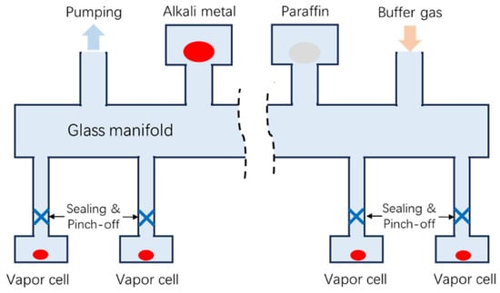
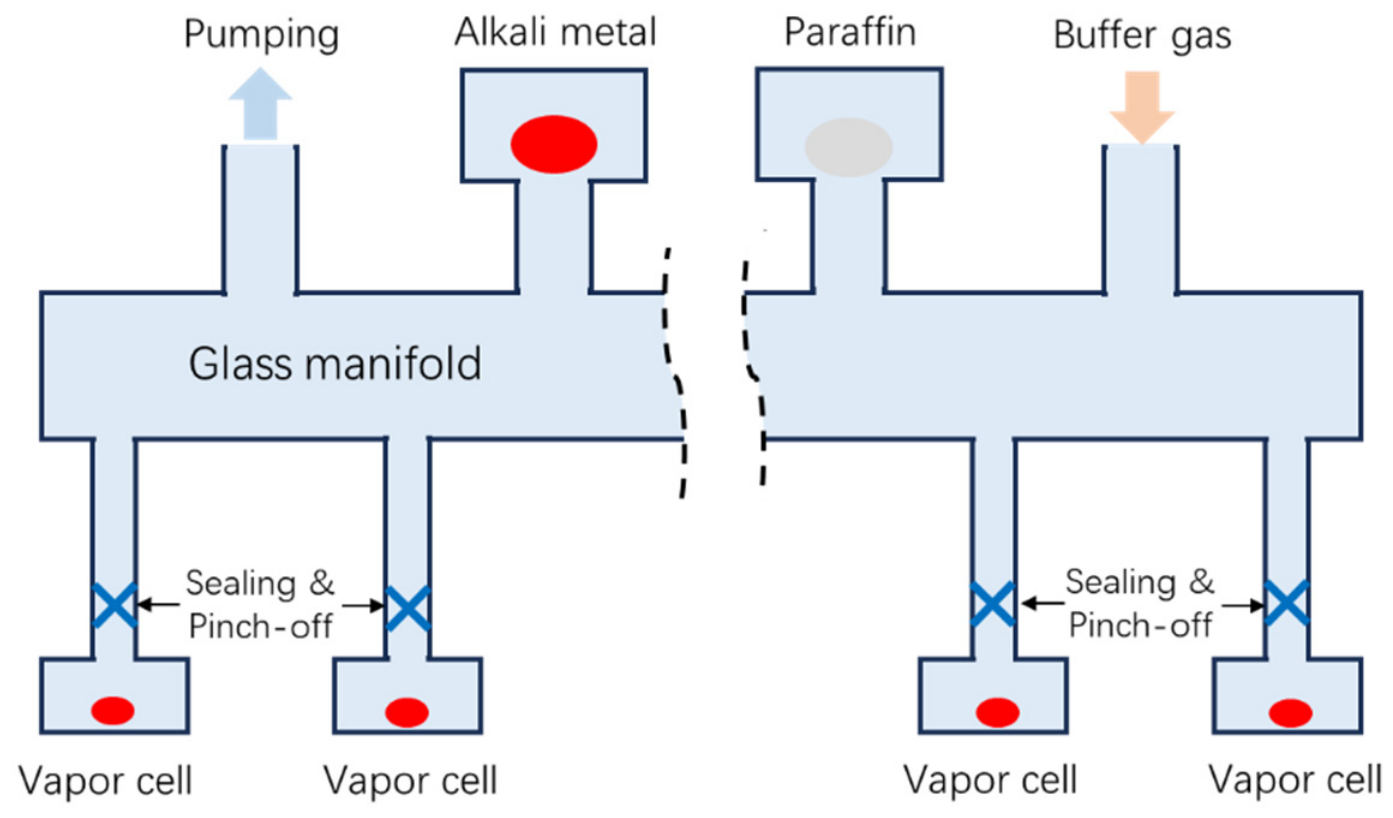


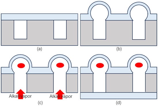
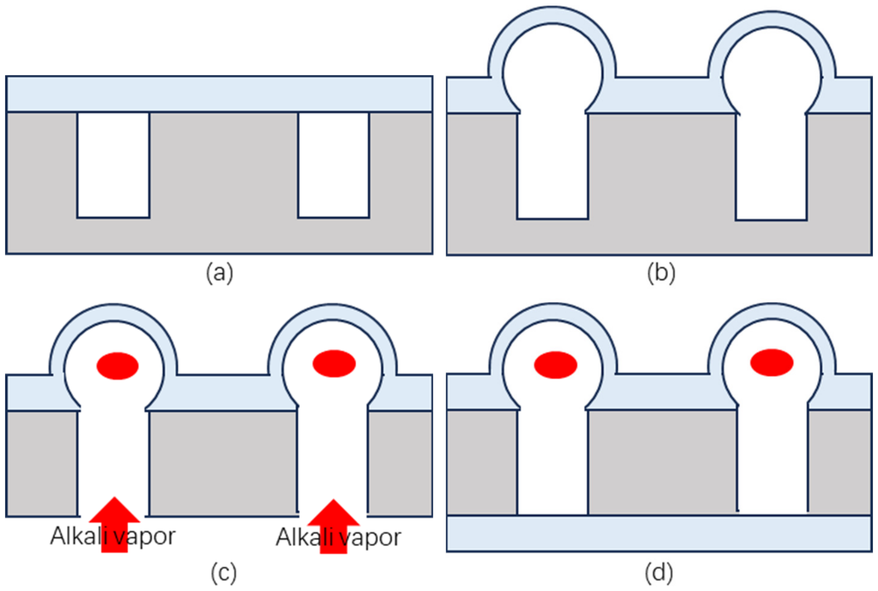
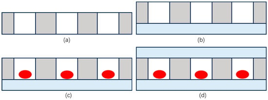
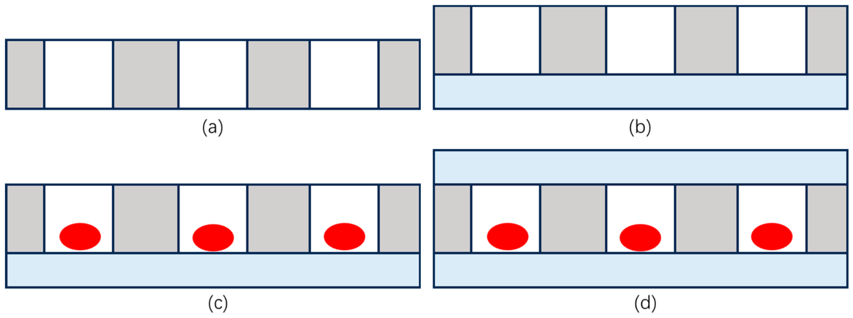
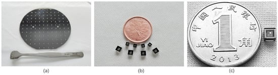
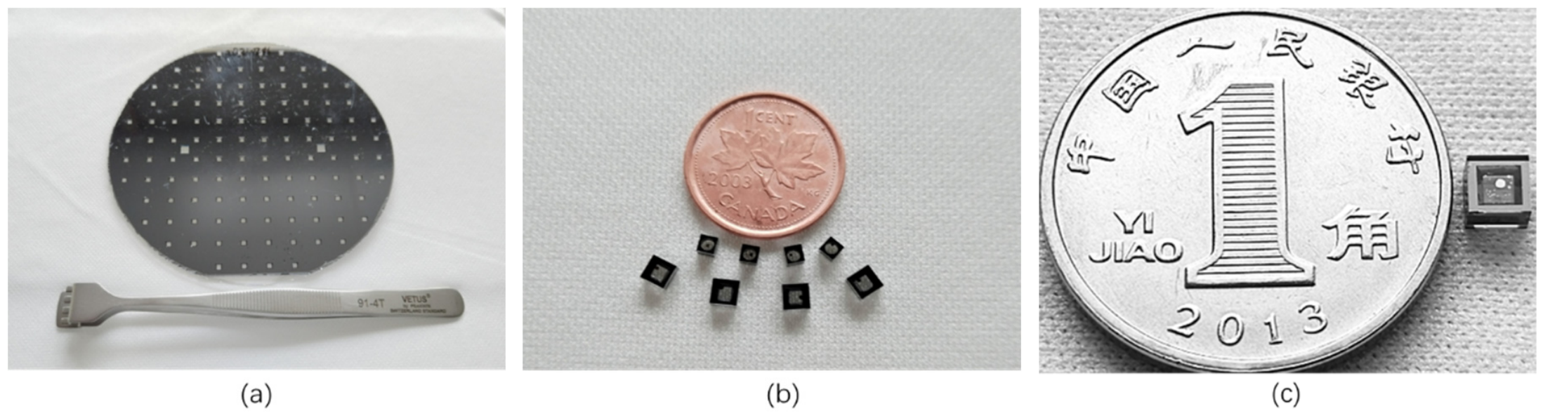
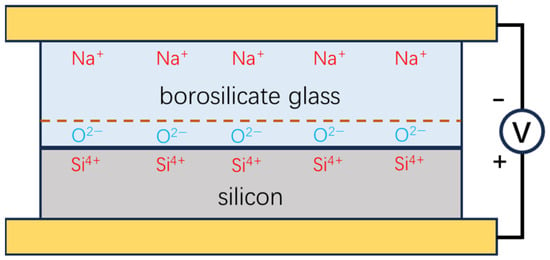
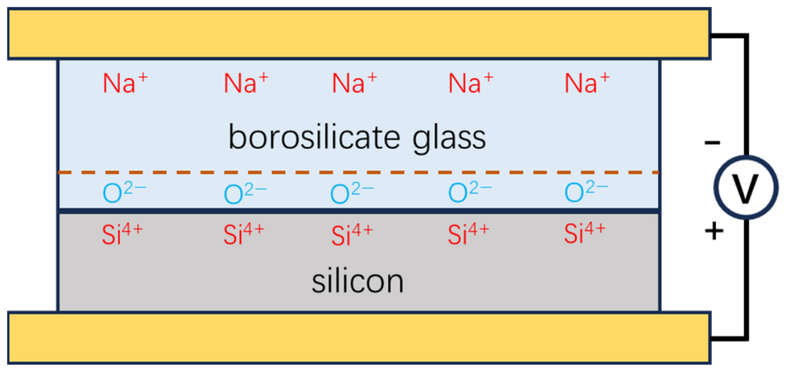
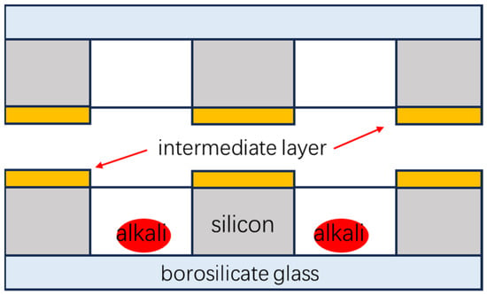
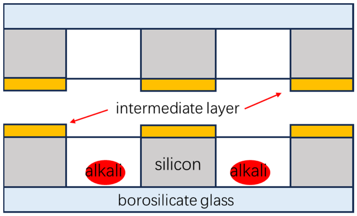
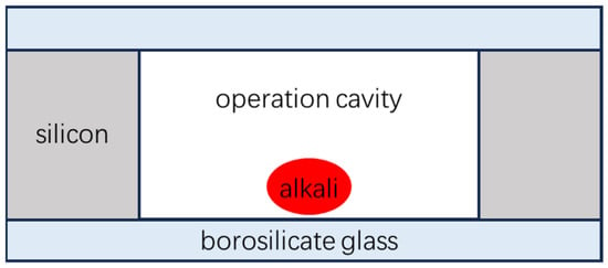
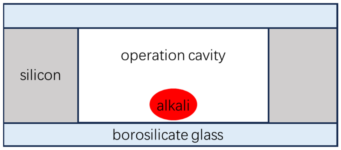
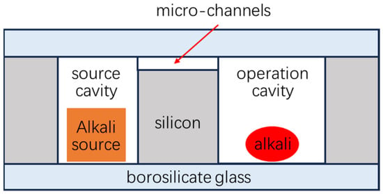
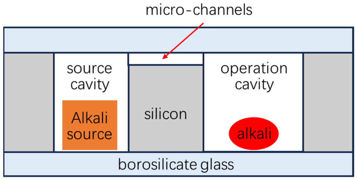
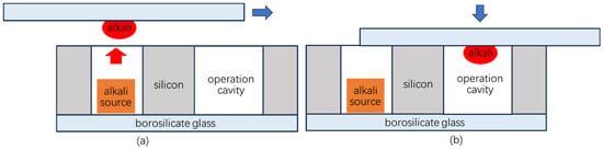
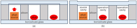
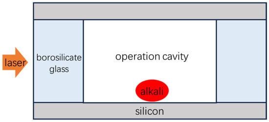
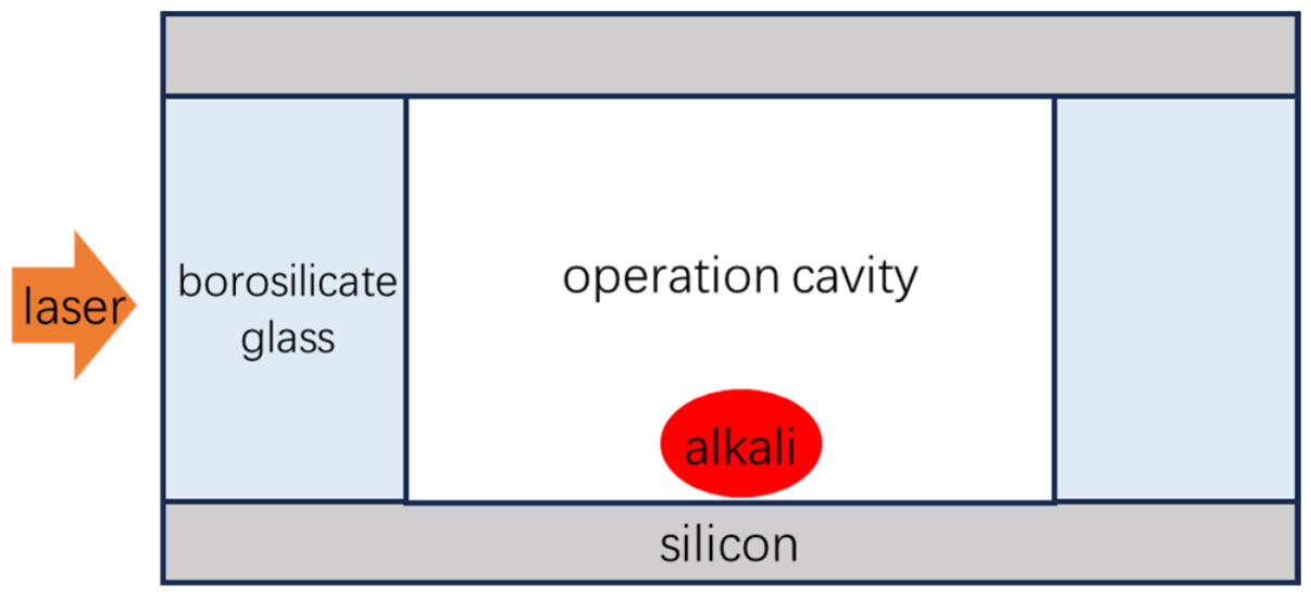
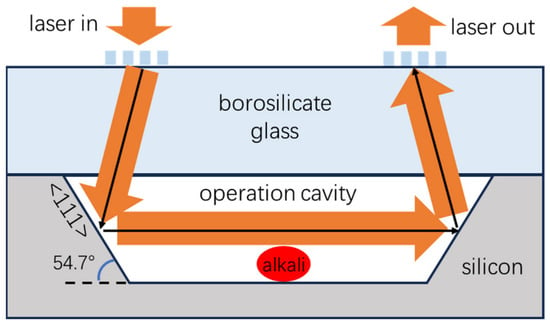
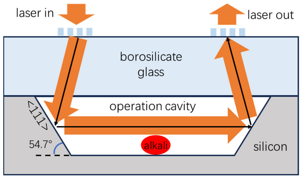

Disclaimer/Publisher’s Note: The statements, opinions and data contained in all publications are solely those of the individual author(s) and contributor(s) and not of MDPI and/or the editor(s). MDPI and/or the editor(s) disclaim responsibility for any injury to people or property resulting from any ideas, methods, instructions or products referred to in the content. |
© 2026 by the authors. Licensee MDPI, Basel, Switzerland. This article is an open access article distributed under the terms and conditions of the Creative Commons Attribution (CC BY) license.