


Abstract
In the last decade, the self-field critical current density Jc(s.f.) in Type-II superconductors has been considered fundamentally limited by a Silsbee-like criterion of Jc(s.f.) = Hc1/λ. We show that this universal limit to self-field critical current density Jc(s.f.) is not universally valid. We present several examples for this in YBa2Cu3O7−δ-type and REBa2Cu3O7−δ thin films and one for Nb thin films and show that calculated Jc(s.f.) using the Silsbee-like criterion using thermodynamic parameters has been substantially exceeded experimentally. We also show that Jc(s.f.) can be significantly improved by incorporation of artificial pinning centers (APCs), further implying that no such universal limit to Jc(s.f.) can exist because such an upper bound, Jc(s.f.) would have to be independent of APCs. These findings call for a revision of the accepted understanding of current-carrying limits in Type-II superconductors and reveal substantial potential for improving Jc in REBCO-based coated conductors through optimization of APCs for large-scale applications, including commercial nuclear fusion.
1. Introduction
Kilometer-long HTS wires based on heteroepitaxial deposition of high-temperature superconductors (HTS) on single-crystal-like substrates have generated tremendous excitement for many envisioned large-scale applications [1,2,3,4,5,6,7,8,9,10]. In particular, energy generation via commercial nuclear fusion is presently of great interest and has created a flurry of interest world-wide [1,2,3,4,5,6,7,8,9,10]. In addition, there are numerous large-scale applications of HTS materials for energy transmission, energy storage and use in electric power devices in the grid. All these large-scale HTS applications, the cost, or the price/performance metric of HTS wires dictates if an application will become commercially viable. A key route to achieve this goal is by significantly increasing the performance of the HTS wires without increasing the process cost. Hence, the question of the maximum performance or the critical current density, Jc, that can be achieved in a HTS wire is of paramount importance and of significant consequence to the field towards achieving conductor price/performance goals for large-scale HTS applications [11,12,13]. A well-known upper bound for the critical current density in any superconductor is the depairing current density Jd, the point at which Cooper pairs are destroyed and the material transitions to a resistive, non-superconducting state. Jd depends on key fundamental thermodynamic parameters such as the penetration depth, the coherence length, and on the measurement temperature. The depairing current density for Type-I superconductors is well-described by the Silsbee rule (proposed in 1917) which states that the depairing current density is the critical current density that, when flowing through the superconductor, induces a magnetic field equal to the critical field (Hc) of the Type-I superconductor causing a sharp breakdown of the superconducting state at the critical field [14], and so Jd = Hc/, where λ is the penetration depth. Unlike Type-I superconductors, in Type-II superconductors, the transition to the normal state is gradual, starting at the lower critical field, Hc1, where a mixed, superconducting and non-superconducting vortex state develops, and the fully resistive, non-superconducting state develops at the upper critical field, Hc2. For most technologically relevant Type-II superconductors, Hc2 is extremely large, whereas Hc1 is comparatively small. Silsbee’s criterion is therefore not applicable for determining the depairing current density in Type-II superconductors.
It has been argued that while the Silsbee criterion when considering the lower critical field, Hc1, does not result in the depairing current density (i.e., Jd is not equal to Hc1/, it may predict a limit to attainable Jc(self-field), thereby providing an “upper limit” to possible Jc(self-field) in a Type-II superconductor. Substituting the standard textbook equation for Hc1 [15] in this formula, Talantsev and Tallon [16] obtain an expression for critical current density in thin-film, Type-II superconductors (as shown in Equation (4) of their paper):
where , is the flux quantum, , is the permeability of free space,London penetration depth (nm) and coherence length (nm). The authors then examined published data in the literature on self-field Jc for various thin-film superconductors, as well as the reported thermodynamic parameters (penetration depth, , and coherence length, ), and then calculated the predicted Jc(s.f) obtained using Equation (1). As noted in their paper, they found no experimental case in which the measured self-field Jc exceeded the value predicted by Equation (1). They therefore proposed that the Jc obtained from Equation (1) represents an “upper limit” to the attainable self-field Jc in thin-film superconductors whose thickness is smaller than the penetration depth . As stated in their paper, the authors were surprised that even for Type-II superconductors, a similar criterion, Jc = Hc1/, provided the “upper limit” to attainable self-field critical current density, Jc(s.f.), and stated that this upper limit is valid for all Type-II superconductors and hence claimed that it was a “universal or fundamental limit” to attainable Jc(s.f.). In their paper, it is emphasized that this fundamental limit also applies to Jc for the second-generation high-temperature superconducting wires (also known as HTS 2G-wires or REBa2Cu3O7−δ tapes or coated conductors) [17], which are the preferred option for high-field applications such as magnets for fusion projects [10]. Moreover, it is stated that the highest Jc(s.f., T) will be achieved with the lowest possible value of , and in REBa2Cu3O7−δ this can only be achieved by full oxygenation (δ→0) and removing all impurity substitution.
2. Methods
In this paper we report the calculation of the predicted universal or fundamental limit to Jc(s.f.), referred to hereon as Jc(max, s.f.)calc. by means of Talantsev and Tallon’s primary Equation (1) listed above [16], using reported experimental values of the fundamental thermodynamic material parameters (the London penetration depth and the coherence length) for cases approaching full oxygenation or for in REBa2Cu3O7−δ and compare the obtained Jc(s.f.) values with experimentally reported Jc(s.f.) values. The Jc(s.f.) is also a reference value for the Jc at high magnetic fields [18]. Moreover, we address the fundamental question of whether the Jc(s.f.) can be affected by extrinsic artificial pinning centers.
First case: Using experimental values of thermodynamic parameters reported by Kiefl, R. F. et al. [19] for YBa2Cu3O6.92, with the effective in-plane penetration depth λab(T→0 K) ≈ 115.3 nm, and coherence length, ξ = 1.5 nm, this fundamental Jc(s.f.) limit calculated using Equation (1) is Jc(max, s.f., T →0 K)calc. ≤ 42 MA/cm2.
Second case: Using data from Sonier et al. [20], for an optimally doped sample of YBa2Cu3O6.95 with Tc = 93 K and having λab = 112 nm, we obtain the same value for this case as for the third case highlighted below.
Third case: Using measured thermodynamic parameters = 112 nm and = 1.6 nm reported by Stangl et al. [21], for a nearly fully oxygenated thin-film of composition YBa2Cu3O7−δ, the calculation for the fundamental limit or Jc(max, s.f.)calc., is shown below:
3. Results and Discussion
Despite the values obtained starting from the reported Equation (1), Stangl et al. [21], report an experimentally measured Jc(s.f., 5 K) of ≈90 MA cm−2 for this undoped YBa2Cu3O7−δ (YBCO) thin-film approaching full oxygenation. The plot of Jc (H) at 5 K in field-range from self-field to 5 T, by Stangl [21] shown in Figure 1 clearly shows significantly higher experimentally obtained Jc than that predicted by Equation (1) using values for thermodynamic parameters λ and ξ measured and reported by them for this film [16]. This Jc(s.f., 5 K) is more than 100% higher than the value of 42 MA/cm2 (which is 44 MA/cm2 if λ and ξ for Stangl’s film shown above are considered) calculated using Talantsev and Tallon’s primary Equation (1). If Stangl et al.’s Jc(s.f.) measurements were made at lower temperatures, approaching 0 K, the Jc would have further increased manifold, even further exceeding Jc(max, s.f.)calc. predicted by Equation (1).
The field and temperature dependences Jc (H, T) of a YBCO—1 vol%BaZrO3 film with self-assembled columnar BZO nanorods fabricated using pulsed laser deposition (PLD), measured in transport by Xu [22,23] are shown in Figure 2. This Figure contains exactly the data presented in Figure 6.4 on page 104 and Figure 6.5 on page 105 of Xu’s thesis [22] and show that Jc for this film in external field at both 10 K and 5 K exceeds the theoretical limit in self-field (42 MA/cm2). The values of Jc(s.f.) are not reported because they exceed the current limit of their transport system, which for the specific bridge geometry and film thickness was 54.6 MA/cm2. Even at this measurement limiting value of 54.6 MA/cm2, the transport Jc(s.f.) is 30% higher than Jc(max, s.f.)calc. = 44 MA/cm2 for YBCO films at full oxygenation, predicted by Equation (1). In addition, if Xu et al.’s measurements were made at lower temperatures, approaching 0 K, the Jc would have increased manifold, even further exceeding this “limit” to self-field Jc. Lastly, since these YBCO films were not fully oxygenated (unlike Stangl’s films), the Jc(s.f.) is expected to further rise significantly upon oxygenation to produce an overdoped state as shown by Stangl.
Figure 1.
Jc (H) for two films: (1) YBa2Cu3O7−δ (YBCO) thin-film approaching full oxygenation from Stangl et al. [21], and (2) (Y,Gd)Ba2Cu3O7−δ (YBCO) thin-film with BaHfO3 additions from Miura et al. [24]. Shown in the figure in blue and green is the Jc(self-field) calculated using the “Universal or fundamental limit” per Equation (1) of 42 MA/cm2 and 44 MA/cm2 and corresponding to the first and third case in the article.
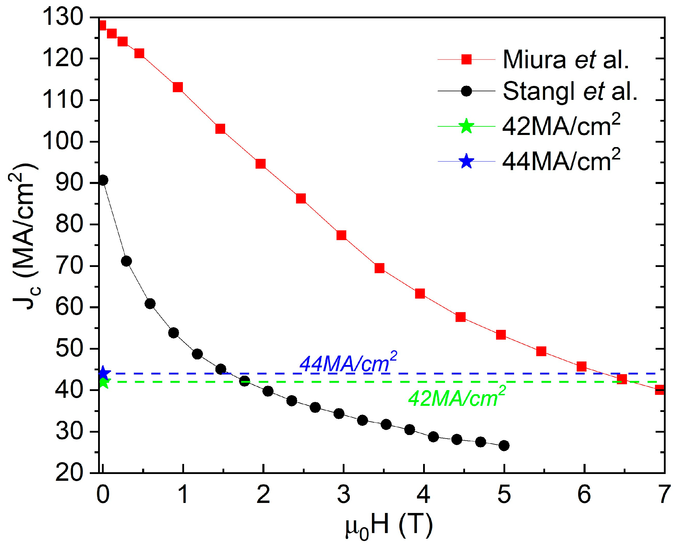
Xu et al. [22,23], also reported an experimentally measured transport Jc(s.f., 4.2 K) ~55 MA/cm2 at 4.2 K for H//c for a thin-film superconductor of composition 15 mol.% Zr-added (Gd, Y)-Ba-Cu-O. This Jc(s.f., 4.2 K) was ~30% higher than that predicted by Equation (1) of 44 MA/cm2. Again, if Xu et al.’s measurements were made at lower temperatures, approaching 0 K, a further pronounced increase in the value of the Jc would have been obtained. Miura et al. [24] reported both a transport and magnetization Jc(s.f., 4.2 K) as well as calculated Jd(4.2 K) for (Y,Gd)Ba2Cu3O7−δ (YBCO) thin films with BaHfO3 additions as a function of carrier concentration. Figure 1 shows experimentally measured Jc(H) at 4.2 K in field-range from self-field to 7 T, by Miura et al. [24] showing significantly higher experimentally obtained Jc than that predicted by Equation (1) (nearly 200%) using values for thermodynamic parameters λ and ξ and as discussed above. Figure 3 shows Jc(s.f., 4.2 K) for three films with carrier concentration, p, equal to 0.18, 0.168 and 0.144. Only the film with p = 0.18 is overdoped and fully oxygenated. Miura et al. also provide experimentally measured values of the thermodynamic parameters, of , for the films as a function of carrier concentration. Table 1 provides a summary of data from Miura along with the predicted Jc(max, s.f.)calc. calculated using Equation (1).
Table 1.
Thermodynamic parameters, , Jc(s.f.) at 4.2 K, Jd (0 K) from Miura et al. [24], and Jc(max, s.f.)calc. calculated using the equation, Jc(max, s.f.)calc. = Hc1/ [16] for (Y,Gd)Ba2Cu3O7−δ (YBCO) thin films with BaHfO3 additions, at different carrier concentration, p.
Figure 2.
Jc (H) for a PLD YBa2Cu3O7−δ + 1vol%BaZrO3 film measured by Xu [22]: (a) Selected data from Figure 6.4 of Xu showing Jc (H) at different temperatures, and (b) Selected data from Figure 6.5 from Xu showing Jc (T) at different applied fields. The dashed line in both figures corresponds to the Jc(max, s.f.)calc. = Hc1/ for YBa2Cu3O7−δ films, calculated by Equation (1).
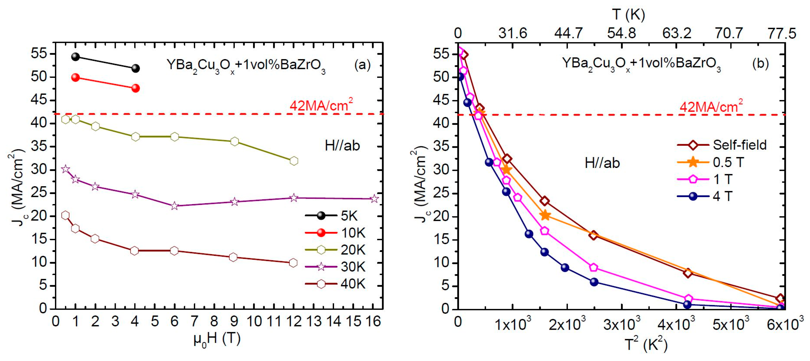
Figure 3.
Jc(s.f.) on the y-axis and Jd(s.f) on the x-axis at 4.2 K for (Y,Gd)Ba2Cu3O7−δ (YBCO) thin-film with BaHfO3 additions from Miura et al. as a function of carrier concentration, p [24], for p = 0.18, 0.168 and 0.144. The solid red line corresponds to Jc equal to 30% of estimated Jd. Also, shown in the plot is a dotted blue line (p = 0.144), a dotted green line (p = 0.168) and a dotted orange line (p = 0.18) corresponding to Jc(max, s.f.)calc. = Hc1/. The highest Jc at p = 0.18 on a CC substrate was 130 MA/cm2 and 150 MA/cm2 for a film on SrTiO3.
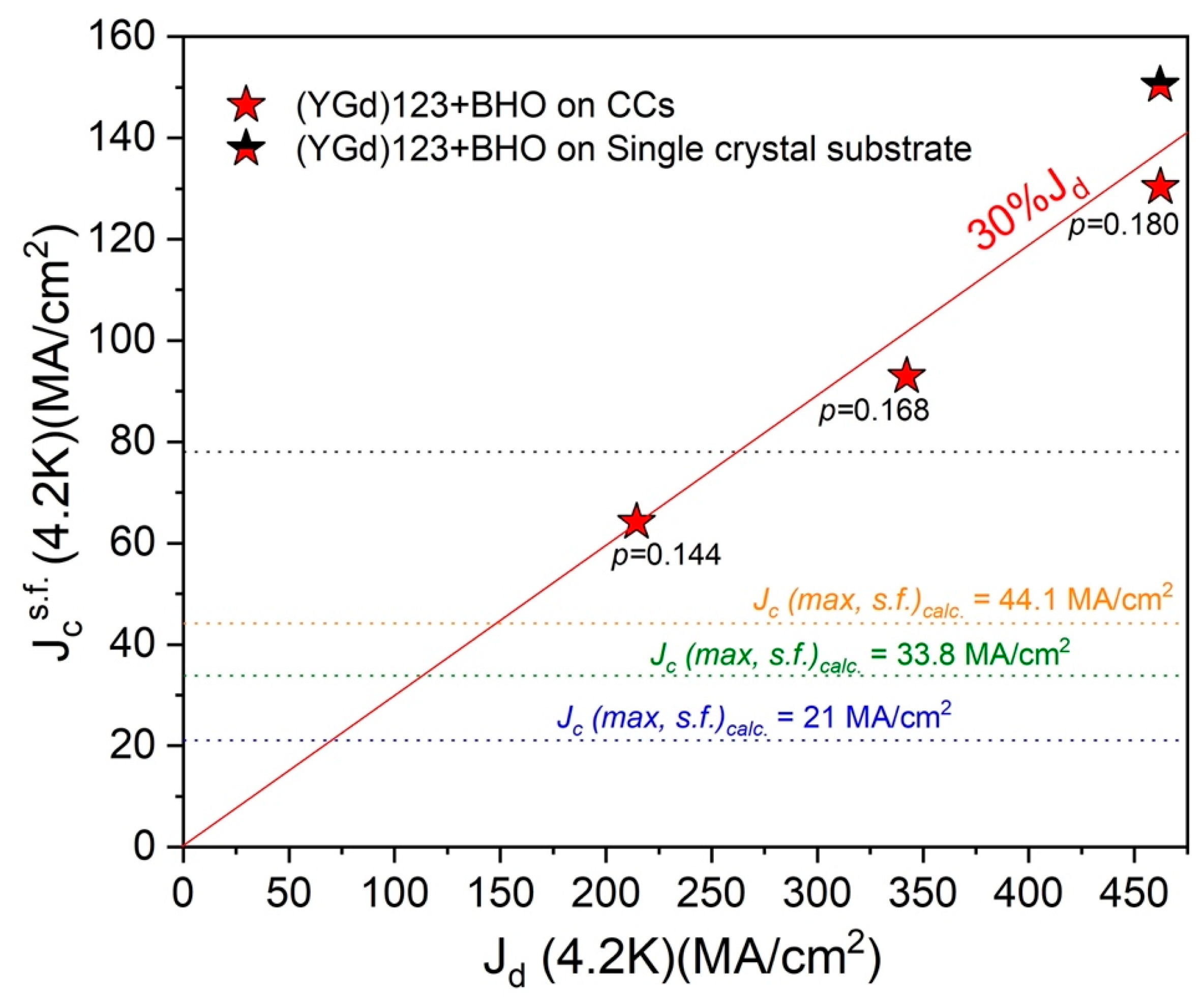
As shown in Table 1, the Jc(s.f., 4.2 K) is 194% higher than the “limit” of 44.1 MA/cm2 for the film on a coated conductor substrate. For the same film deposited on single-crystal, SrTiO3 substrate, the Jc(s.f., 4.2 K) is 240% higher than this “limit”. For the incompletely oxygenated film corresponding to carrier concentration, p = 0.168, the Jc(s.f., 4.2 K) is 166% higher than the predicted limit of 33.8 MA/cm2 for the film on a coated conductor substrate, calculated using the measured for this film. Lastly, for the incompletely oxygenated film corresponding to carrier concentration, p = 0.144, the Jc(s.f., 4.2 K) is 195% higher than the “limit” of 21.0 MA/cm2 for the film on a coated conductor substrate, calculated using the measured thermodynamic parameters, , for this film. Again, if Miura et al.’s measurements were made at lower temperatures, approaching 0 K, the Jc would have further increased by a significant margin, substantially exceeding the predicted limit to attainable self-field Jc. Even for films that were not fully oxygenated with p = 0.168 and 0.144, the Jc exceeded the predicted limit of 44.1 MA/cm2 for a fully oxygenated film. In Figure 3, the solid red line corresponds to Jc equal to 30% of estimated Jd, the dotted blue line (p = 0.144), the dotted green line (p = 0.168) and the dotted orange line (p = 0.18) corresponds to the Jc calculated using the equation Jc(max, s.f.)calc. = Hc1/. It can be seen that in all cases the experimentally obtained Jc significantly exceeds the Jc(max, s.f.)calc. limit predicted by primary Equation (1). In fact, for all three values of the carrier concentration, the measured Jc exceeds the highest Jc calculated for the fully oxygenated, overdoped film shown by the orange dotted line. Figure 1 also shows Jc (H, 4.2 K) for the film on a coated conductor substrate which was overdoped in comparison to the Stangl’s films and the Jc (max, s.f.)calc. It can be seen that the Jc(s.f.) limit predicted by Equation (1) has been greatly exceeded.
If one can find a way to lower the value of the penetration depth, , then the “fundamental limit” to Jc(s.f.) increases. Talantsev and Tallon [17] proposed doing so by using the lowest reported values for GdxY1−xBa2Cu3O6+y single-crystals by Perag-Barnea et al. [25] of λa = 103 ± 8 nm and λb = 80 ± 5 nm, giving an effective in-plane penetration depth of λeff = λab = √λaλb = 91 nm. Perag-Barnea et al. obtained the magnetic penetration depth by relating the number of Gd ions exposed to the microwave magnetic field to the frequency-integrated intensity of the observed ESR transitions. Combined with a value ξ = 1.5 nm, Talantsev and Tallon calculated Jc(s.f., T →0 K) ≤ 78 MA/cm2. However, this value of λeff has never been experimentally confirmed in another study on GdxY1−xBa2Cu3O6+y single-crystals or reported for any GdxY1−xBa2Cu3O6+y film on a coated conductor substrate or on a single-crystal substrate such as SrTiO3. Regardless, even using this value of 78 MA/cm2 as the fundamental limit to Jc(s.f.) for GdxY1−xBa2Cu3O6+y films, the Jc is exceeded by 67% for a film on a coated conductor substrate and as shown in Figure 3 and Table 1. Figure 3 shows a dotted black line at 78 MA/cm2. The experimentally measured Jc exceeds this value by ~15% for p = 0.168, by ~67% for p = 0.18 for films on a coated conductor substrate and by ~92% for a film on a single-crystal substrate with p = 0.18.
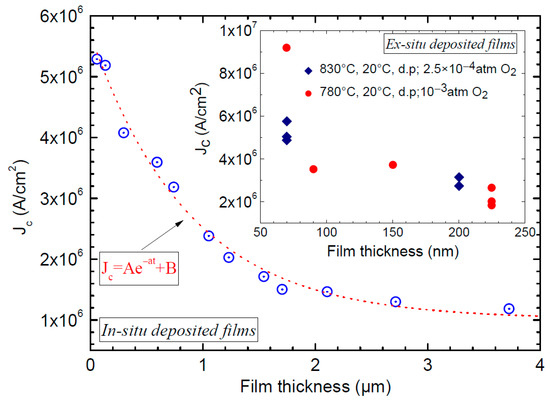
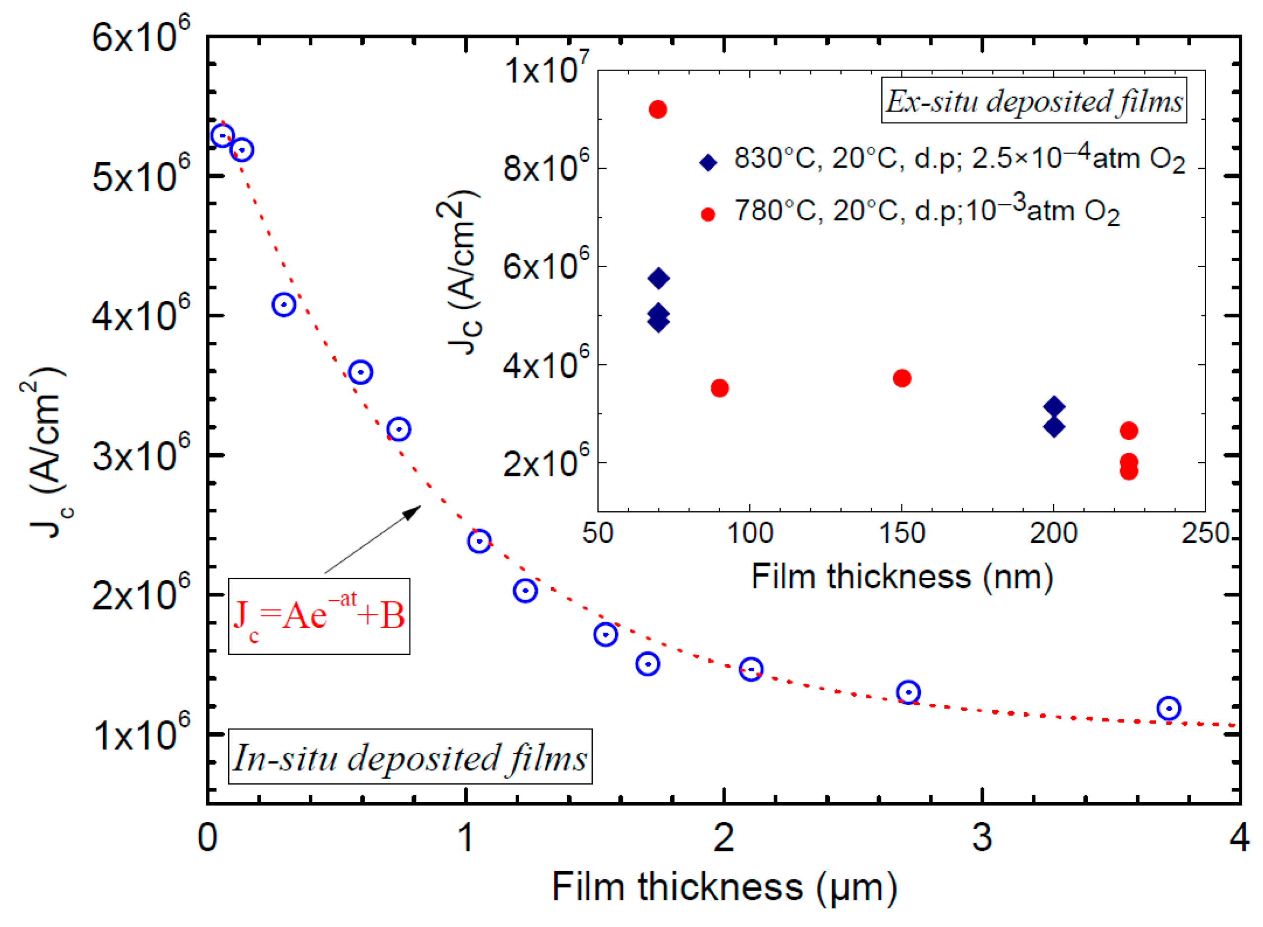
In their paper [16], the authors argued that their universal self-field Jc limit applies only to films with thicknesses smaller than , since films thicker than allow flux entry from the edges, implying that the proposed universal limit would no longer hold in such cases. However, this consideration becomes relevant only if the thickness dependence of Jc in REBCO films were such that Jc continued to increase for thicknesses exceeding . In contrast, experimental evidence shows that the self-field Jc increases rapidly at small film thicknesses [26,27,28], and in most cases grows exponentially for thicknesses below the penetration depth. This is clearly shown in Figure 1 of Matsui et al. [26], Figure 9 of McIntyre et al. [27] and Figure 3 in Foltyn et al. [28]. McIntyre et al. [27] reported on films made by chemical solution deposition with thicknesses ranging from 70 nm to 300 nm and Foltyn et al. [28], reported on films made using pulsed laser ablation with thicknesses ranging from 65 nm to 6.4 μm, and in both cases, the Jc(s.f.), increased exponentially at lower film thicknesses below 150 nm as shown in Figure 4 for in situ PLD films upto 4 μm in thickness. In fact, it is well appreciated that the high self-field Jc of very thin films is due to a dense array of misfit dislocations at the film/substrate interface, raising the self-field Jc of such very thin films [29,30,31], with the implication that these defects are causing the Jc(s.f.) to be increased. Given this trend of the thickness dependence of Jc(s.f.), it can be reasonably expected that Jc(s.f., 4.2 K) of films reported in Xu et al., Stangl et al. and Miura et al. will further increase quite substantially at lower film thicknesses, even more significantly surpassing the presumed universal or fundamental limit of self-field Jc.
Figure 4.
Jc(s.f.) of thin films increases exponentially with decrease in thickness, for in situ PLD films [28] and also for ex situ films as shown in the inset [27]. In both cases, the Jc(s.f.) increases exponentially when film thickness is much smaller than the typical REBCO penetration depth.
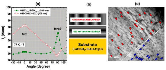
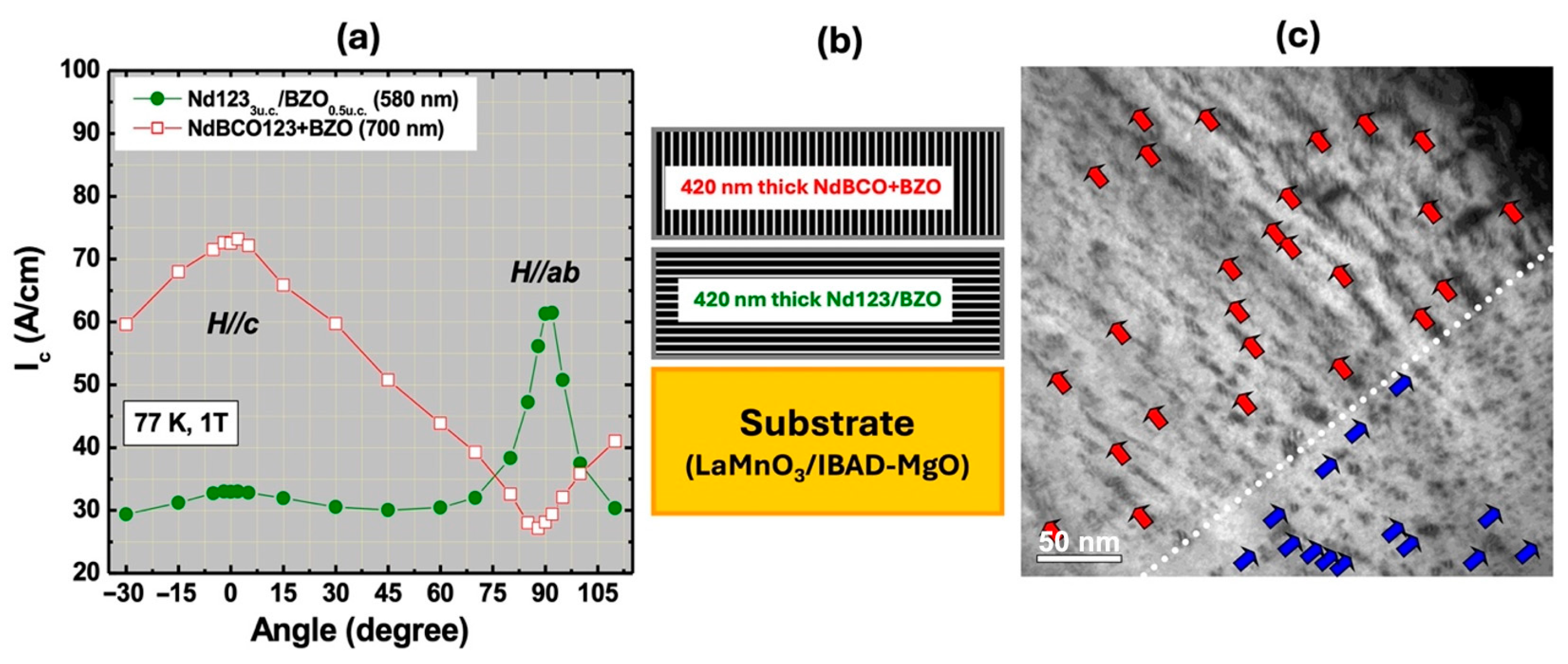
For extreme Type-II superconductors such as REBa2Cu3O7−δ (REBCO), where Hc2 is very high (150 T for optimally doped YBCO [32]) and Hc1 is very low (~34–35 mT for optimally doped YBCO [33]), the self-field generated by the current exceeds Hc1 even at low currents and the sample enters the mixed state where the Jc is then determined by vortex-pinning. Hence, it is not surprising that a self-field Jc calculated using the formula, Jc = Hc1/, was experimentally exceeded. In reference [16], the authors claim that self-field Jc is fully independent of pinning. They noted a single exception reported by Schindler et al. [34], where neutron irradiation increased the self-field Jc from 19.4 to 32 MA/cm2. However, this result was ruled out on the grounds that Schindler et al. employed a high electric-field criterion. It is correct that artificial pinning centers (APCs) generated via irradiation after film growth can in most cases lower Jc (s.f.) due to a loss of effective cross-section area and/or damage to the two-dimensional CuO2 planes. However, there are many additional studies in the literature that show the Jc (s.f.) to increase very substantially with introduction of APCs. In contrast to post-growth irradiation, where APC formation is decoupled from the film-growth process, non-irradiative methods for introducing APCs directly influence film growth, morphology, microstructure, crystallographic texture, and epitaxy, and in most cases lead to a significant enhancement of the Jc (s.f.). Here, we cite only a few studies showing clear increase in Jc (s.f.) via introduction of APCs—see Figure 4 of Miura et al. [24], Figure 4 of Diez-Sierra et al. [35], Figure 3 of Vaimala et al. [36], Figure 2 of Jha et al. [37] and Figure 4 of Jha et al. [38]. As mentioned previously, this can also potentially be a secondary effect due to improved film microstructure, morphology, texture, etc., with the introduction of APCs. In Wee et al. [39], defect engineering resulted in a massive increase in transport Jc(s.f., 77 K), from 1.4 MA/cm2 to 2.5 MA/cm2 (~78% increase in Jc(s.f.)) for a film of NdBa2Cu3O7−δ with the incorporation of engineered, non-superconducting, nanoscale APCs compared to a NdBa2Cu3O7−δ with no engineered APCs incorporated. Figure 5 shows that for this film, 50% of the film was nanostructured such that the BaZrO3 (BZO) nanorods were aligned perpendicular to the film and for the other 50% of the film, the BZO nanorods were aligned parallel to the c-axis of YBCO [39]. This film had a combined thickness of 0.86 μm.
Figure 5.
Hybrid NdBa2Cu3Ox + BaZrO3 (BZO) films, with a total thickness of 0.86 μm, deposited using PLD on a coated conductor substrate [39]. The bottom half of the film has BZO nanorods aligned parallel to the substrate surface or parallel to the ab-plane of NdBa2Cu3Ox, and the top half of the film with BZO nanorods aligned perpendicular to the substrate surface or parallel to the c-axis of NdBa2Cu3Ox. (a) Angular dependence of Ic at 77 K, 1 T, showing that pinning corresponds to the orientation of BZO. (b) Schematic of film cross-section showing alignment of BZO in film and (c) high-resolution transmission electron microscopy image showing alignment of BZO nanostructures. The dashed white line separates the two halves of the film with the blue and red arrows pointing to BZO nanostructures in bottom and top halves of the film.
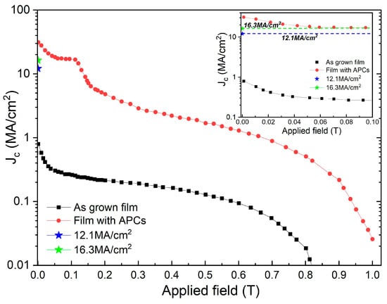
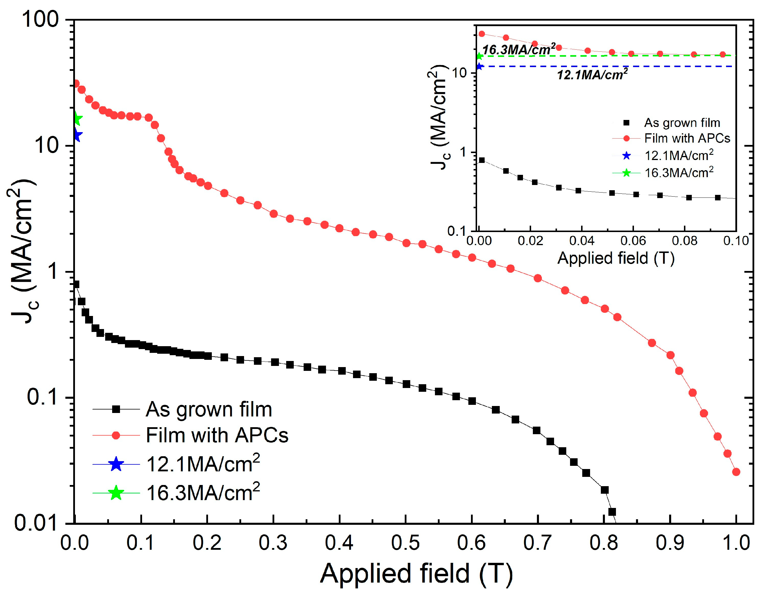
While the available data for HTS materials other than REBCO is limited, we further show that this universal or fundamental limit to Jc(s.f.) also does not apply to other Type-II superconductors. We consider Nb, a classical Type-II superconductor. Dinner et al. reported achievement of extremely high critical current density in Nb thin films via through-thickness arrays of APCs via ion-milling through anodized aluminum oxide thin- film templates [40]. They reported experimentally measured transport Jc (H) in Nb thin films with optimized APCs (in terms of size and spacing) to be 50 times greater than Nb film with no APCs at self-field [40]. In fact, Figure 6 shows Jc (H) at 5.0 K for a Nb thin-film with and without APCs from Dinner et al. [40] with the field applied perpendicular to the film surface. The black points and line correspond to Jc for the film with no APCs. The red points and line correspond to Jc for the film with nanoscale APCs. The transport Jc(s.f., 5 K) of the Nb film with no APCs or pinning centers was ~0.6 MA/cm2 and the transport Jc (s.f., 5 K) of the Nb film with optimized, through thickness APCs was 30 MA/cm2. This further clearly demonstrates that in Type-II superconductors, Jc(s.f.) is also dependent on pinning. Therefore, our analysis shows that (Y,Gd)Ba2Cu3O7−δ (YBCO) thin films with BaHfO3 and through-thickness arrays of APCs via ion-milling through anodized aluminium oxide thin-film templates in Nb thin films were both extremely effective in increasing self-field Jc.
Figure 6.
Jc (H) at 5K for a Nb thin-film with and without APCs from Dinner et al. [40]. The black points and line correspond to Jc for the film with no APCs. The red points and line correspond to Jc for the film with nanoscale APCs. Also shown in the figure with a blue and green asterisk are Jc values calculated using Equation (1) for coherence length, ξ, of 23.1 nm and 40 nm, respectively. Inset: a magnification in the range 0 T and 0.1 T is shown to better visualize the higher values of the experimentally obtained self-field Jc for the film with APCs (red points) than the ones calculated using the so-called predicted maximum attainable self-field Jc using expression, Jc(max, s.f.)calc. = Hc1/.
The penetration depth, , for these films was 120 nm [40,41] and the coherence length, ξ(5 K) = 40 nm [41]. However, since, from Ginzburg-Landau theory, , with Tc = 7.5 K (from Dinner et al., page 4), it results ξ0 = 23.1 nm at T = 0 K. Based on these thermodynamic parameters, Table 2 shows the calculated values of Jc(max, s.f.)calc. using the primary equation mentioned above corresponding to Jc(max, s.f.)calc. = Hc1/.
Table 2.
Thermodynamic parameters, from Dinner et al. [40], and Jc(max, s.f.)calc. calculated using the equation, Jc(max, s.f.)calc. = Hc1/ [16] for Nb thin films.
In Figure 6, the blue and green asterisk correspond to these Jc values calculated using the equation reported in reference [16], for coherence length, ξ, of 23.1 nm (@ 0 K) and 40 nm (@ 5 K), respectively. As shown in Table 2 above, the experimentally obtained transport Jc(s.f.) of 30 MA/cm2 is ~100% higher than that predicted by [16]. The inset of Figure 6 clearly shows the experimentally obtained self-field Jc compared to that calculated using the so-called predicted maximum attainable self-field Jc using expression, Jc (max, s.f.)calc. = Hc1/. The transport measurements reported in Dinner et al. [40] were made on 12 μm wide bridges, wide enough for the geometrical issues to be not relevant. A validation for this stems from the fact that for same bridge width, the Nb film with no APCs only had a transport Jc(s.f.) of ~0.6 MA/cm2.
Although Xu [22], published in 2012, reported transport Jc of YBCO thin films on CC substrates, Xu et al. [23], published in 2014, reported transport Jc of (Y,Gd)BCO thin films on CC substrates, and Dinner et al. [40], published in 2011, reported transport Jc of Nb thin films, these references were not considered in reference [16]. In addition, significant enhancements to transport Jc(s.f.) of YBCO thin films on CC substrates via incorporation of APCs have been shown recently in many reports [21,22,23,24,35,36,37,38,39,40]. These references now cast strong doubt on the premise of a universal or fundamental limit to Jc(s.f.) for Type-II superconductors given by the expression, Jc(max, s.f.)calc = Hc1/, as their primary equation.
In short, we have shown the following:
- (1)
- Experimentally obtained, Jc(s.f.), significantly higher than that calculated using Talantsev and Tallon’s primary Equation (1) [16] have been reported (by Xu et al. [22,23], Stangl et al. [21] and Miura et al. [24]) for YBa2Cu3O7−δ-type and REBa2Cu3O7−δ thin films and by Dinner et al. [40] for Nb films, rendering predictions of Jc(s.f.) by a Silsbee-like criterion to be incorrect. A summary of the samples, materials, parameters, and self-field critical current densities considered in this work is reported in Table 3:Table 3. Summary of samples and self-field critical current density results.
- (2)
- Due to the established, rapid decrease in the critical current density with thickness, for films thinner than the films reported in point (1) above, we expect an even higher Jc(s.f.) further exceeding the Jc (max, s.f.)calc. limit predictions, and
- (3)
- Jc(s.f.) can be significantly increased with introduction of extrinsic artificial pinning centers [35,36,37,38,39,40], further rendering the Jc(max, s.f.)calc. limit using a Silsbee-like criterion invalid.
In an alternative analysis, Mastushita and Kiuchi estimated the upper limit of achievable critical current density via optimization of APCs under the influence of kinetic energy using Ginzburg-Landau theory [42]. They estimated the upper limit of the achievable Jc to be 67% of the depairing current density in the London limit [42]. They argue that the strong flux pinning by self-assembled nanorods when optimized, could provide such high Jc approaching this upper limit of 67% of Jd [42]. Self-assembled nanorods or nanocolumns consisting of perovskite (BaMO3) and double perovskite (Ba2RETaO6 and Ba2RETaO6) [43,44,45,46,47,48,49,50,51,52,53,54,55,56] nanorods have been shown to form controllable self-assembled microstructures with greatly enhanced Jc and flux-pinning. Very high-Jc has also been achieved in microstructures comprising randomly oriented nanoparticles of Y2BaCuOx [57], BaZrO3 [58,59,60,61] and RE2O3 [62,63]. A critical-current-by-design paradigm to tailor and enhance Jc using time-dependent Ginzburg-Landau simulations coupled with Monte-Carlo and molecular dynamics has been proposed to further optimize Jc [11]. The data collectively demonstrate that Jc(s.f.) is a highly tunable quantity governed by microstructural design, suggesting that optimization strategies rather than fixed limits should guide practical materials development, and that further opportunities are present for theorists to develop deeper physical insights to more accurately predict a limiting Jc(s.f.) in thin-film Type-II superconducting films.
4. Conclusions
It was shown that the “universal or fundamental limit” to self-field Jc calculated using a Silsbee-like criterion of Jc(max, s.f.)calc. = Hc1/, for Type-II superconductors is not valid. This was established via detailed calculations for several YBa2Cu3O7−δ-type and REBa2Cu3O7−δ thin films and then comparing the obtained Jc(max, s.f.)calc. values to experimental Jc(s.f.) values. This was also shown to be the case for another Type-II superconductor, Nb, where experimental Jc(s.f.) was found to be significantly higher than the predicted fundamental limit calculated via the equation, Jc(max, s.f.)calc. = Hc1/, using reported thermodynamic parameters for the film. In addition, it was established that in Type-II superconductors, the Jc(s.f.) also depends on extrinsic pinning centers, a key fundamental question in the field. The fact that Jc(s.f.), in superconductors with different substrates, can be significantly improved by incorporation of artificial pinning centers (APC’s), further implies that no universal limit to Jc(s.f.) can exist because for such a universal and fundamental limit to exist, Jc(max, s.f.)calc. would have to be independent of extrinsic pinning centers and different pinning mechanisms.
This leads to an important conclusion that the performance of REBa2Cu3O7−δ based thin-film coated conductors have not reached their limit to attainable Jc(s.f.). Since the depairing current density in (Y,Gd)Ba2Cu3O7−δ (YBCO) thin films with BaHfO3 is still a factor of three to four higher than the highest experimentally achieved Jc, the potential headroom for increasing Jc is still enormous. There remains substantial room for enhancement of Jc of commercial coated conductors which could significantly improve the price-to-performance ratio of high-temperature superconducting wires. Such progress would directly accelerate the deployment of superconductors across large-scale technologies, including energy generation (commercial nuclear fusion), transmission (superconducting ac and dc cables), and storage (superconducting magnetic energy storage systems, SMES), as well as in energy-efficient devices such as motors, generators, and fault-current limiters. Given the recent excitement generated due to the possibility of commercial nuclear fusion enabled by coated conductor HTS wires, this is an extremely important and key point to be considered in scaling-up fabrication of HTS wires.
Author Contributions
Conceptualization, A.G. (Amit Goyal) and M.P.; methodology, A.G. (Amit Goyal) and M.P.; validation, A.G. (Amit Goyal), R.K., A.G. (Armando Galluzzi) and M.P.; formal analysis, A.G. (Amit Goyal); investigation, R.K. and A.G. (Armando Galluzzi); data curation, R.K. and A.G. (Armando Galluzzi); writing—original draft preparation, A.G. (Amit Goyal) and M.P.; writing—review and editing, A.G. (Amit Goyal), R.K., A.G. (Armando Galluzzi) and M.P.; visualization, A.G. (Amit Goyal), R.K., A.G. (Armando Galluzzi) and M.P.; supervision, A.G. (Amit Goyal) and M.P.; funding acquisition, A.G. (Amit Goyal) and M.P. All authors have read and agreed to the published version of the manuscript.
Funding
This work was supported by the Office of Naval Research (ONR), Grant No. N00014-21-1-2534 on proposal titled “Defect-engineering to probe attainable flux-pinning in coated conductors”. The content reported is solely the responsibility of the authors and does not represent the official views of the Office of Naval Research. M.P. and A. Galluzzi acknowledge support from the EU COST Actions CA19108 Hi- SCALE, CA20116 OPERA, and CA21144 SUPERQUMAP. M.P. acknowledges partial financial support by the PRIN 2022 PNRR Project QUESTIONs Grant No. P2022KWFBH.
Institutional Review Board Statement
Not applicable.
Informed Consent Statement
Not applicable.
Data Availability Statement
The original contributions presented in this study are included in the article. Further inquiries can be directed to the corresponding authors.
Conflicts of Interest
The authors declare no conflicts of interest.
References
- Meschini, S.; Laviano, F.; Ledda, F.; Pettinari, D.; Testoni, R.; Torsello, D.; Panella, B. Review of Commercial Nuclear Fusion Projects. Front. Energy Res. 2023, 11, 1157394. [Google Scholar] [CrossRef] [Scilit]
- Hartwig, Z.S.; Vieira, R.F.; Sorbom, B.N.; Badcock, R.A.; Bajko, M.; Beck, W.K.; Castaldo, B.; Craighill, C.L.; Davies, M.; Estrada, J.; et al. VIPER: An Industrially Scalable High-Current High-Temperature Superconductor Cable. Supercond. Sci. Technol. 2020, 33, 11LT01. [Google Scholar] [CrossRef] [Scilit]
- Higashikawa, K.; Ide, A.; Bian, W.; Kiss, T. Development of Superconducting Cable with Energy Storage Function and Evaluation of Its Functionality in DC Microgrid with Renewable Energy Sources. IEEE Trans. Appl. Supercond. 2023, 33, 5400405. [Google Scholar] [CrossRef] [Scilit]
- Chow, C.C.T.; Ainslie, M.D.; Chau, K.T. High Temperature Superconducting Rotating Electrical Machines: An Overview. Energy Rep. 2023, 9, 1124–1156. [Google Scholar] [CrossRef] [Scilit]
- Santos, B.M.O.; Dias, F.J.M.; Trillaud, F.; Sotelo, G.G.; de Andrade Junior, R. A Review of Technology Readiness Levels for Superconducting Electric Machinery. Energies 2023, 16, 5955. [Google Scholar] [CrossRef] [Scilit]
- Papageorgiou, P.G.; Oureilidis, K.O.; Christoforidis, G.C. A Systematic Review of Hybrid Superconducting Magnetic/Battery Energy Storage Systems: Applications, Control Strategies, Benefits, Limitations and Future Prospects. Renew. Sustain. Energy Rev. 2023, 183, 113436. [Google Scholar] [CrossRef] [Scilit]
- Stryczewska, H.D.; Boiko, O.; Stępień, M.A.; Lasek, P.; Yamazato, M.; Higa, A. Selected Materials and Technologies for Electrical Energy Sector. Energies 2023, 16, 4543. [Google Scholar] [CrossRef] [Scilit]
- Marchionini, B.; Eckroad, S.; Serri, L.; Angeli, G.; Ohsaki, H.; Mosteller, D.; Martini, L. High Temperature Superconductivity Application Readiness Map—Energy Delivery—Transmission, Substation and Distribution. IEEE Trans. Appl. Supercond. 2023, 33, 5401405. [Google Scholar] [CrossRef] [Scilit]
- Hernando, C.; Munilla, J.; García-Tabarés, L.; Pedraz, G. Optimization of High Power SMES for Naval Applications. IEEE Trans. Appl. Supercond. 2023, 33, 5700205. [Google Scholar] [CrossRef] [Scilit]
- Mitchell, N.; Zheng, J.; Vorpahl, C.; Corato, V.; Sanabria, C.; Segal, M.; Sorbom, B.; Slade, R.; Brittles, G.; Bateman, R.; et al. Superconductors for Fusion: A Roadmap. Supercond. Sci. Technol. 2021, 34, 103001. [Google Scholar] [CrossRef] [Scilit]
- Glatz, A.; Sadovskyy, I.A.; Welp, U.; Kwok, W.K.; Crabtree, G.W. The Quest for High Critical Current in Applied High-Temperature Superconductors. J. Supercond. Nov. Magn. 2020, 33, 127–141. [Google Scholar] [CrossRef] [Scilit]
- Pęczkowski, P.; Zalecki, R.; Zachariasz, P.; Szostak, E.; Piętosa, J.; Turek, M.; Pyszniak, K.; Zając, M.; Czub, J.; Gondek, Ł. Deterioration of the 2G HTS Tapes by the Ne+ Ions Irradiation (250 KeV). Appl. Surf. Sci. 2023, 636, 157780. [Google Scholar] [CrossRef] [Scilit]
- Pęczkowski, P.; Zachariasz, P.; Jastrzębski, C.; Piętosa, J.; Drzymała, E.; Gondek, Ł. On the Superconductivity Suppression in Eu1−xPrxBa2Cu3O7−δ. Materials 2021, 14, 3503. [Google Scholar] [CrossRef] [Scilit] [PubMed]
- Silsbee, F.B. Note on Electrical Conduction in Metals at Low Temperatures. J. Frankl. Inst. 1917, 184, 111. [Google Scholar] [CrossRef] [Scilit]
- Poole, C.; Farach, H.; Creswick, R.; Prozorov, R. Superconductivity; Academic Press: Cambridge, MA, USA; Elsevier: Amsterdam, The Netherlands, 2007; ISBN 978-0-12-088761-3. [Google Scholar]
- Talantsev, E.F.; Tallon, J.L. Universal Self-Field Critical Current for Thin-Film Superconductors. Nat. Commun. 2015, 6, 7820. [Google Scholar] [CrossRef] [Scilit] [PubMed]
- Talantsev, E.F.; Tallon, J.L. Fundamental Nature of the Self-Field Critical Current in Superconductors. arXiv 2024, arXiv:2409.16758. [Google Scholar] [CrossRef] [Scilit]
- Jaroszynski, J.; Constantinescu, A.M.; Miller, G.; Xu, A.; Francis, A.; Murphy, T.; Larbalestier, D.C. Rapid Assessment of REBCO CC Angular Critical Current Density Jc(B, T = 4.2 K, θ) Using Torque Magnetometry up to at Least 30 Tesla. Supercond. Sci. Technol. 2022, 35, 095009. [Google Scholar] [CrossRef] [Scilit]
- Kiefl, R.F.; Hossain, M.D.; Wojek, B.M.; Dunsiger, S.R.; Morris, G.D.; Prokscha, T.; Salman, Z.; Baglo, J.; Bonn, D.A.; Liang, R.; et al. Direct Measurement of the London Penetration Depth in YBa2Cu3O6.92 Using Low-Energy ΜsR. Phys. Rev. B Condens. Matter Mater. Phys. 2010, 81, 180502. [Google Scholar] [CrossRef] [Scilit]
- Sonier, J.E.; Brewer, J.H.; Kiefl, R.F. ΜSR Studies of the Vortex State in Type-II Superconductors. Rev. Mod. Phys. 2000, 72, 769–811. [Google Scholar] [CrossRef] [Scilit]
- Stangl, A.; Palau, A.; Deutscher, G.; Obradors, X.; Puig, T. Ultra-High Critical Current Densities of Superconducting YBa2Cu3O7-δ Thin Films in the Overdoped State. Sci. Rep. 2021, 11, 8176. [Google Scholar] [CrossRef] [Scilit]
- Xu, A. Flux Pinning Study of REBa2Cu3O7-δ Coated Conductors for High Field Magnet Applications. Ph.D Thesis, Florida State University, Tallahassee, FL, USA, 2012. [Google Scholar]
- Xu, A.; Delgado, L.; Khatri, N.; Liu, Y.; Selvamanickam, V.; Abraimov, D.; Jaroszynski, J.; Kametani, F.; Larbalestier, D.C. Strongly Enhanced Vortex Pinning from 4 to 77 K in Magnetic Fields up to 31 T in 15 Mol.% Zr-Added (Gd, Y)-Ba-Cu-O Superconducting Tapes. APL Mater. 2014, 2, 46111. [Google Scholar] [CrossRef] [Scilit]
- Miura, M.; Tsuchiya, G.; Harada, T.; Sakuma, K.; Kurokawa, H.; Sekiya, N.; Kato, Y.; Yoshida, R.; Kato, T.; Nakaoka, K.; et al. Thermodynamic Approach for Enhancing Superconducting Critical Current Performance. NPG Asia Mater. 2022, 14, 85. [Google Scholar] [CrossRef] [Scilit]
- Pereg-Barnea, T.; Turner, P.J.; Harris, R.; Mullins, G.K.; Bobowski, J.S.; Raudsepp, M.; Liang, R.; Bonn, D.A.; Hardy, W.N. Absolute Values of the London Penetration Depth in YBa2Cu3O6+y Measured by Zero Field ESR Spectroscopy on Gd Doped Single Crystals. Phys. Rev. B 2004, 69, 184513. [Google Scholar] [CrossRef] [Scilit]
- Matsui, H.; Tsukada, K.; Tsuchiya, T.; Sohma, M.; Yamaguchi, I.; Manabe, T.; Kumagai, T. Thickness Dependence of the Critical-Current Density and Its Relation to near-Interface Crystal Imperfections in Fluorine-Free-MOD YBCO Films. IEEE Trans. Appl. Supercond. 2011, 21, 2933–2936. [Google Scholar] [CrossRef] [Scilit]
- McIntyre, P.C.; Cima, M.J.; Smith, J.A.; Hallock, R.B.; Siegal, M.P.; Phillips, J.M. Effect of Growth Conditions on the Properties and Morphology of Chemically Derived Epitaxial Thin Films of Ba2YCu3O7-x on (001) LaAlO3. J. Appl. Phys. 1992, 71, 1868–1877. [Google Scholar] [CrossRef] [Scilit]
- Foltyn, S.R.; Tiwari, P.; Dye, R.C.; Le, M.Q.; Wu, X.D. Pulsed Laser Deposition of Thick YBa2Cu3O7−δ Films with Jc≥1 MA/Cm2. Appl. Phys. Lett. 1993, 63, 1848–1850. [Google Scholar] [CrossRef] [Scilit]
- Foltyn, S.R.; Civale, L.; Macmanus-Driscoll, J.L.; Jia, Q.X.; Maiorov, B.; Wang, H.; Maley, M. Materials Science Challenges for High-Temperature Superconducting Wire. Nat. Mater. 2007, 6, 631–642. [Google Scholar] [CrossRef] [Scilit] [PubMed]
- Matsui, H.; Yamaguchi, I. Enhancement of Self-Field Critical Current Density by Several-Tens-MeV Ion Irradiation in YBa2Cu3O7 Films Prepared by Fluorine-Free Metal-Organic Deposition. Jpn. J. Appl. Phys. 2022, 61, 043001. [Google Scholar] [CrossRef] [Scilit]
- Wang, H.; Foltyn, S.R.; Arendt, P.N.; Jia, Q.X.; Zhang, X. Identification of the Misfit Dislocations at YBa2Cu3O7-δ/SrTiO3 Interface Using Moiré Fringe Contrast. Phys. C Supercond. Appl. 2006, 444, 1–4. [Google Scholar] [CrossRef] [Scilit]
- Grissonnanche, G.; Cyr-Choinière, O.; Laliberté, F.; René de Cotret, S.; Juneau-Fecteau, A.; Dufour-Beauséjour, S.; Delage, M.-È.; LeBoeuf, D.; Chang, J.; Ramshaw, B.J.; et al. Direct Measurement of the Upper Critical Field in Cuprate Superconductors. Nat. Commun. 2014, 5, 3280. [Google Scholar] [CrossRef] [Scilit]
- Joshi, K.R.; Nusran, N.M.; Tanatar, M.A.; Cho, K.; Meier, W.R.; Bud’Ko, S.L.; Canfield, P.C.; Prozorov, R. Measuring the Lower Critical Field of Superconductors Using Nitrogen-Vacancy Centers in Diamond Optical Magnetometry. Phys. Rev. Appl. 2019, 11, 014035. [Google Scholar] [CrossRef] [Scilit]
- Schindler, W.; Roas, B.; Saemann-Ischenko, G.; Schultz, L.; Gerstenberg, H. Anisotropic Enhancement of the Critical Current Density of Epitaxial YBa2Cu3O7-x Films by Fast Neutron Irradiation. Phys. C Supercond. Appl. 1990, 169, 117–122. [Google Scholar] [CrossRef] [Scilit]
- Díez-Sierra, J.; López-Domínguez, P.; Rijckaert, H.; Rikel, M.; Hänisch, J.; Khan, M.Z.; Falter, M.; Bennewitz, J.; Huhtinen, H.; Schäfer, S.; et al. High Critical Current Density and Enhanced Pinning in Superconducting Films of YBa2Cu3O7-δ Nanocomposites with Embedded BaZrO3, BaHfO3, BaTiO3, and SrZrO3 Nanocrystals. ACS Appl. Nano Mater. 2020, 3, 5542–5553. [Google Scholar] [CrossRef] [Scilit]
- Vaimala, T.; Aye, M.M.; Rivasto, E.; Zhao, Y.; Huhtinen, H.; Paturi, P. Maximizing Flux Pinning in YBCO Coated Conductor Films for High-Field Applications. Phys. C Supercond. Appl. 2024, 624, 1354565. [Google Scholar] [CrossRef] [Scilit]
- Jha, A.K.; Matsumoto, K.; Horide, T.; Saini, S.; Mele, P.; Yoshida, Y.; Awaji, S. Systematic Variation of Hybrid APCs Into YBCO Thin Films for Improving the Vortex Pinning Properties. IEEE Trans. Appl. Supercond. 2015, 25, 8000505. [Google Scholar] [CrossRef] [Scilit]
- Jha, A.K.; Matsumoto, K.; Horide, T.; Saini, S.; Ichinose, A.; Mele, P.; Yoshida, Y.; Awaji, S. Evaluation of Temperature Dependent Vortex Pinning Properties in Strongly Pinned YBa2Cu3O7-δ Thin Films with Y2BaCuO5 Nanoinclusions. Superconductivity 2024, 9, 100087. [Google Scholar] [CrossRef] [Scilit]
- Wee, S.H.; Goyal, A.; Zuev, Y.L.; Cantoni, C. Tuning Flux-Pinning in Epitaxial NdBa2Cu3O7-δ Films via Engineered, Hybrid Nanoscale Defect Structures. Appl. Phys. Express 2008, 1, 111702. [Google Scholar] [CrossRef] [Scilit]
- Dinner, R.B.; Robinson, A.P.; Wimbush, S.C.; MacManus-Driscoll, J.L.; Blamire, M.G. Depairing Critical Current Achieved in Superconducting Thin Films with Through-Thickness Arrays of Artificial Pinning Centers. Supercond. Sci. Technol. 2011, 24, 055017. [Google Scholar] [CrossRef] [Scilit]
- Gubin, A.I.; Il’in, K.S.; Vitusevich, S.A.; Siegel, M.; Klein, N. Dependence of Magnetic Penetration Depth on the Thickness of Superconducting Nb Thin Films. Phys. Rev. B 2005, 72, 064503. [Google Scholar] [CrossRef] [Scilit]
- Matsushita, T.; Kiuchi, M. Theoretical Estimation of the Upper Limit of Critical Current Density by Flux Pinning in Superconductors under the Influence of Kinetic Energy. Appl. Phys. Express 2019, 12, 023004. [Google Scholar] [CrossRef] [Scilit]
- Goyal, A.; Kang, S.; Leonard, K.J.; Martin, P.M.; Gapud, A.A.; Varela, M.; Paranthaman, M.; Ijaduola, A.O.; Specht, E.D.; Thompson, J.R.; et al. Irradiation-Free, Columnar Defects Comprised of Self-Assembled Nanodots and Nanorods Resulting in Strongly Enhanced Flux-Pinning in YBa2Cu3O7-δ Films. Supercond. Sci. Technol. 2005, 18, 1533–1538. [Google Scholar] [CrossRef] [Scilit]
- Yamada, Y.; Takahashi, K.; Kobayashi, H.; Konishi, M.; Watanabe, T.; Ibi, A.; Muroga, T.; Miyata, S.; Kato, T.; Hirayama, T.; et al. Epitaxial Nanostructure and Defects Effective for Pinning in Y(RE) Ba2Cu3O7-x Coated Conductors. Appl. Phys. Lett. 2005, 87, 132502. [Google Scholar] [CrossRef] [Scilit]
- Mukaida, M.; Horide, T.; Kita, R.; Horii, S.; Ichinose, A.; Yoshida, Y.; Miura, O.; Matsumoto, K.; Yamada, K.; Mori, N. Critical Current Density Enhancement around a Matching Field in ErBa2Cu3O7-δ Films with BaZrO3 Nano-Rods. Jpn. J. Appl. Phys. 2005, 44, L952. [Google Scholar] [CrossRef] [Scilit]
- Peurla, M.; Paturi, P.; Stepanov, Y.P.; Huhtinen, H.; Tse, Y.Y.; Bódi, A.C.; Raittila, J.; Laiho, R. Optimization of the BaZrO3 Concentration in YBCO Films Prepared by Pulsed Laser Deposition. Supercond. Sci. Technol. 2006, 19, 767–771. [Google Scholar] [CrossRef] [Scilit]
- Kang, S.; Goyal, A.; Li, J.; Gapud, A.A.; Martin, P.M.; Heatherly, L.; Thompson, J.R.; Christen, D.K.; List, F.A.; Paranthaman, M.; et al. High-Performance High-Tc Superconducting Wires. Science 2006, 311, 1911–1914. [Google Scholar] [CrossRef] [Scilit] [PubMed]
- Wee, S.H.; Gao, Y.; Zuev, Y.L.; More, K.L.; Meng, J.; Zhong, J.; Stocks, G.M.; Goyal, A. Self-Assembly of Nanostructured, Complex, Multication Films via Spontaneous Phase Separation and Strain-Driven Ordering. Adv. Funct. Mater. 2013, 23, 1912–1918. [Google Scholar] [CrossRef] [Scilit]
- Sebastian, M.A.P.; Reichart, J.N.; Ratcliff, M.M.; Bullard, T.J.; Burke, J.L.; Ebbing, C.R.; Panasyuk, G.Y.; Tsai, C.F.; Zhang, W.; Huang, J.; et al. Study of the Flux Pinning Landscape of YBCO Thin Films with Single and Mixed Phase Additions BaMO3 + Z: M = Hf, Sn, Zr and Z = Y2O3, Y211. IEEE Trans. Appl. Supercond. 2017, 27, 7500805. [Google Scholar] [CrossRef] [Scilit]
- Wu, Y.; Shi, J.; Guo, C.; Jiang, G.; Suo, H.; Wu, W.; Li, X.; Wang, Y.; Zhao, Y. Ultra-Fast Dynamic Deposition of EuBa2Cu3O7−δ-BaHfO3 Nanocomposite Films: Self-Assembly Structure Modulation and Flux Pinning Behaviors. Mater. Des. 2022, 224, 111406. [Google Scholar] [CrossRef] [Scilit]
- Tsuchiya, Y.; Funaki, S.; Ozaki, T.; Kiuchi, M.; Yoshida, Y. Magnetic Relaxation in Commercial REBCO Tapes With and Without Artificial Pinning Centers. IEEE Trans. Appl. Supercond. 2022, 32, 4604405. [Google Scholar] [CrossRef] [Scilit]
- Selvamanickam, V.; Chen, Y.; Zhang, Y.; Guevara, A.; Shi, T.; Yao, Y.; Majkic, G.; Lei, C.; Galtsyan, E.; Miller, D.J. Effect of Rare-Earth Composition on Microstructure and Pinning Properties of Zr-Doped (Gd,Y)Ba2Cu3O7-δ Superconducting Tapes. Supercond. Sci. Technol. 2012, 25, 045012. [Google Scholar] [CrossRef] [Scilit]
- Wee, S.H.; Goyal, A.; Zuev, Y.L.; Cantoni, C.; Selvamanickam, V.; Specht, E.D. Formation of Self-Assembled, Double-Perovskite, Ba2YNbO6 Nanocolumns and Their Contribution to Flux-Pinning and Jc in Nb-Doped YBa2Cu3O7-δ Films. Appl. Phys. Express 2010, 3, 023101. [Google Scholar] [CrossRef] [Scilit]
- Wee, S.H.; Goyal, A.; Specht, E.D.; Cantoni, C.; Zuev, Y.L.; Selvamanickam, V.; Cook, S. Enhanced Flux Pinning and Critical Current Density via Incorporation of Self-Assembled Rare-Earth Barium Tantalate Nanocolumns within YBa2Cu3O7-δ Films. Phys. Rev. B 2010, 81, 140503. [Google Scholar] [CrossRef] [Scilit]
- Rizzo, F.; Augieri, A.; Kursumovic, A.; Bianchetti, M.; Opherden, L.; Sieger, M.; Hühne, R.; Hänisch, J.; Meledin, A.; Van Tendeloo, G.; et al. Pushing the Limits of Applicability of REBCO Coated Conductor Films through Fine Chemical Tuning and Nanoengineering of Inclusions. Nanoscale 2018, 10, 8187–8195. [Google Scholar] [CrossRef] [Scilit]
- MacManus-Driscoll, J.L.; Wimbush, S.C. Processing and Application of High-Temperature Superconducting Coated Conductors. Nat. Rev. Mater. 2021, 6, 587–604. [Google Scholar] [CrossRef] [Scilit]
- Haugan, T.; Barnes, P.N.; Wheeler, R.; Melsenkothen, F.; Sumption, M. Addition of Nanoparticle Dispersions to Enhance Flux Pinning of the YBa2Cu3O7-x Superconductor. Nature 2004, 430, 867–870. [Google Scholar] [CrossRef] [Scilit] [PubMed]
- Takao, Y.; Awano, M.; Takagi, H. Preparation and Properties of Ba2YCu3O7-x-BaZrO3 Superconductive Composite by Spray Drying Method. J. Ceram. Soc. Jpn. 1994, 102, 237–240. [Google Scholar] [CrossRef] [Scilit]
- Takao, Y.; Awano, M.; Kuwahara, Y.; Murase, Y. Preparation of Oxide Superconductive Composite by an Electrostatic Mixing Process. Sens. Actuators B Chem. 1996, 31, 131–133. [Google Scholar] [CrossRef] [Scilit]
- Macmanus-Driscoll, J.L.; Foltyn, S.R.; Jia, Q.X.; Wang, H.; Serquis, A.; Civale, L.; Maiorov, B.; Hawley, M.E.; Maley, M.P.; Peterson, D.E. Strongly Enhanced Current Densities in Superconducting Coated Conductors of YBa2Cu3O7-x + BaZrO3. Nat. Mater. 2004, 3, 439–443. [Google Scholar] [CrossRef] [Scilit]
- Puig, T.; Gutierrez, J.; Obradors, X. Impact of High Growth Rates on the Microstructure and Vortex Pinning of High-Temperature Superconducting Coated Conductors. Nat. Rev. Phys. 2024, 6, 132–148. [Google Scholar] [CrossRef] [Scilit]
- Molodyk, A.; Samoilenkov, S.; Markelov, A.; Degtyarenko, P.; Lee, S.; Petrykin, V.; Gaifullin, M.; Mankevich, A.; Vavilov, A.; Sorbom, B.; et al. Development and Large Volume Production of Extremely High Current Density YBa2Cu3O7 Superconducting Wires for Fusion. Sci. Rep. 2021, 11, 2084. [Google Scholar] [CrossRef] [Scilit]
- Rupich, M.W.; Verebelyi, D.T.; Zhang, W.; Kodenkandath, T.; Li, X. Metalorganic Deposition of YBCO Films for Second-Generation High-Temperature Superconductor Wires. MRS Bull. 2004, 29, 572–578. [Google Scholar] [CrossRef] [Scilit]

Disclaimer/Publisher’s Note: The statements, opinions and data contained in all publications are solely those of the individual author(s) and contributor(s) and not of MDPI and/or the editor(s). MDPI and/or the editor(s) disclaim responsibility for any injury to people or property resulting from any ideas, methods, instructions or products referred to in the content. |
© 2026 by the authors. Licensee MDPI, Basel, Switzerland. This article is an open access article distributed under the terms and conditions of the Creative Commons Attribution (CC BY) license.