


Abstract
The absorber layer thicknesses of tandem photovoltaic devices containing hybrid organic–inorganic lead halide perovskite absorbers are optimized under AM 1.5 and AM 0 solar irradiance using external quantum efficiency (EQE) simulations. Using the EQE modeling approach derived from analysis of ellipsometric spectra collected from complete single-junction perovskite, all-perovskite tandem, and copper indium gallium diselenide (CIGS) thin film solar cells, structural–optical models are developed for two high-efficiency tandem solar cell configurations from their published EQE spectra. These configurations include a superstrate all-perovskite device and a substrate perovskite/CIGS device. These models serve as realistic and practical baselines for optimizing device performance under different circumstances. By increasing the thicknesses of an all-perovskite tandem superstrate device’s wide Eg and narrow Eg absorber layers from 350 and 975 nm to 356 and 1200 nm, the Jsc may be increased from 15.81 to 15.94 mA/cm2 under AM 1.5 illumination. This corresponds to a potential increase in efficiency from 25.83 to 26.05% when using reported open circuit voltage (Voc) and fill factor (FF). Under AM 0, an increase in absorber layer thickness to 310 and 1200 nm increases the Jsc from 18.56 to 19.72 mA/cm2, which corresponds to an increase in efficiency from 30.33 to 32.22%. By increasing the thickness of the perovskite layer in a perovskite/CIGS substrate device from 500 to 615 nm, the Jsc may be increased from 18.84 to 19.65 mA/cm2 assuming AM 1.5 illumination. This change would increase efficiency from 23.74 to 24.76%. Under AM 0 illumination, an increase in the perovskite thickness to 512 nm results in an increase in predicted Jsc from 23.13 to 23.34 mA/cm2. This corresponds to a predicted efficiency increase from 29.15 to 29.41%. This modeling approach provides a stable platform for practical evaluation of different superstrate and substrate design tandem solar cells with perovskite semiconductors as at least one of their absorber layers.
1. Introduction
Tandem photovoltaic (PV) devices offer the potential of greatly increased efficiencies compared to single-junction PV devices. Hybrid organic–inorganic lead halide-based perovskites and copper indium gallium diselenide (CIGS) semiconducting absorber layers feature tunable band gap (Eg) energies that vary with composition, making them promising absorber layer materials for wide and narrow Eg subcells in tandem PV devices and other optoelectronic devices [1]. Current record efficiencies of tandem devices containing perovskite absorbers are 30.1% for all-perovskite devices, 34.6% for perovskite/Si devices, and 24.6% for perovskite/CIGS devices [2]. Researchers constantly explore excursions in process parameter space such as layer thicknesses to increase efficiency, and in the case of tandem devices, the number of adjustable parameters can be numerous. By simulating the external quantum efficiency (EQE) spectra of tandem devices, the effects of parameter adjustments on short circuit current density (Jsc) can be readily determined. This would be helpful in aiding experimentalists in improving their devices. This work first focuses on how to develop physically realistic optical–structural models for a superstrate design in an all-perovskite tandem device and a substrate design in a perovskite/CIGS tandem device from reported experimental EQE. This capability enables a better framework for establishing practical limitations relative to simulated device performance. The simulated all-perovskite device is based on the work of Wen et al. at Nanjing University, which held the record for all-perovskite tandem device efficiency of 26.4% in 2021 [2,3]. The simulated perovskite/CIGS device is based on the work of Jošt et al. at the Helmholtz Center Berlin for Materials and Energy, which held the record for perovskite/CIGS tandem device efficiency of 24.2% from February 2020—January 2025 [2,4]. Baseline structural–optical models for these devices are developed from analysis of their EQE spectra, building from our previous work in modeling perovskite and CIGS solar cell EQE using input parameters from spectroscopic ellipsometry [5,6,7,8,9,10,11]. This ability enables the generation of a realistic optical–structural model from reported EQE spectra which in turn can be used to identify future Jsc optimization pathways. As many solar cell devices are optimized for terrestrial applications at AM 1.5 solar illumination when reported in the literature, this approach can be applied to identify how current matching in tandem devices can be achieved under AM 0 solar illumination for space applications.
2. Methods
EQE simulations are performed using free, publicly available software (e-ARC 3.0) that uses a transfer matrix approach where reflectance and absorbance spectra of each layer are calculated [9]. The thicknesses of the absorber layers are divided into multiple sections, and the contribution to the EQE of some sections are reduced until the simulated EQE spectra match the experimental EQE spectra, simulating the effect of electronic losses [8]. The resulting spectra are used to calculate Jsc. The Jsc of each absorber layer and the equivalent Jsc loss of all other layers are calculated by integrating the absorbance spectra multiplied by the photon energy and solar irradiance spectrum with respect to wavelength [8]. Jsc losses due to reflectance and electronic losses are similarly calculated using their respective spectra. Irradiance of each layer is calculated by integrating the absorbance spectra multiplied by the solar irradiance spectrum [10].
For the all-perovskite superstrate device, planar interfaces are assumed at all wavelengths. For the CIGS/perovskite substrate device, planar interfaces are assumed at wavelengths less than 750 nm, and minimized reflection loss due to scattering is assumed at wavelengths greater than or equal to 750 nm. This is done to better approximate the shape of the experimental EQE spectra. Polycrystalline perovskite and CIGS thin films often exhibit scattering at long wavelengths comparable to their grain size [6,11]. Complex dielectric function spectra and thicknesses of each layer are input parameters.
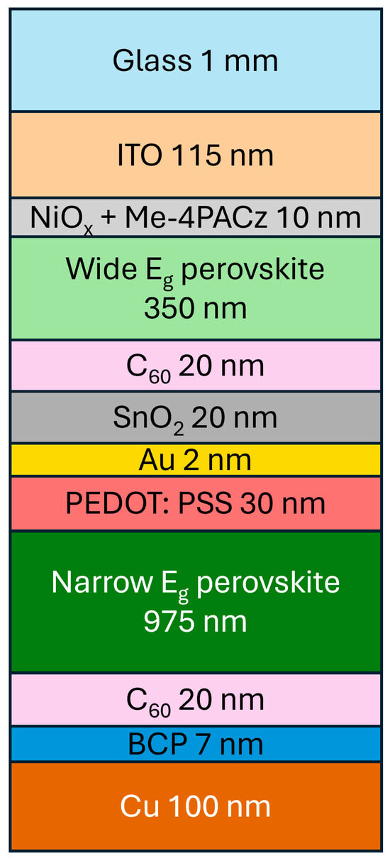
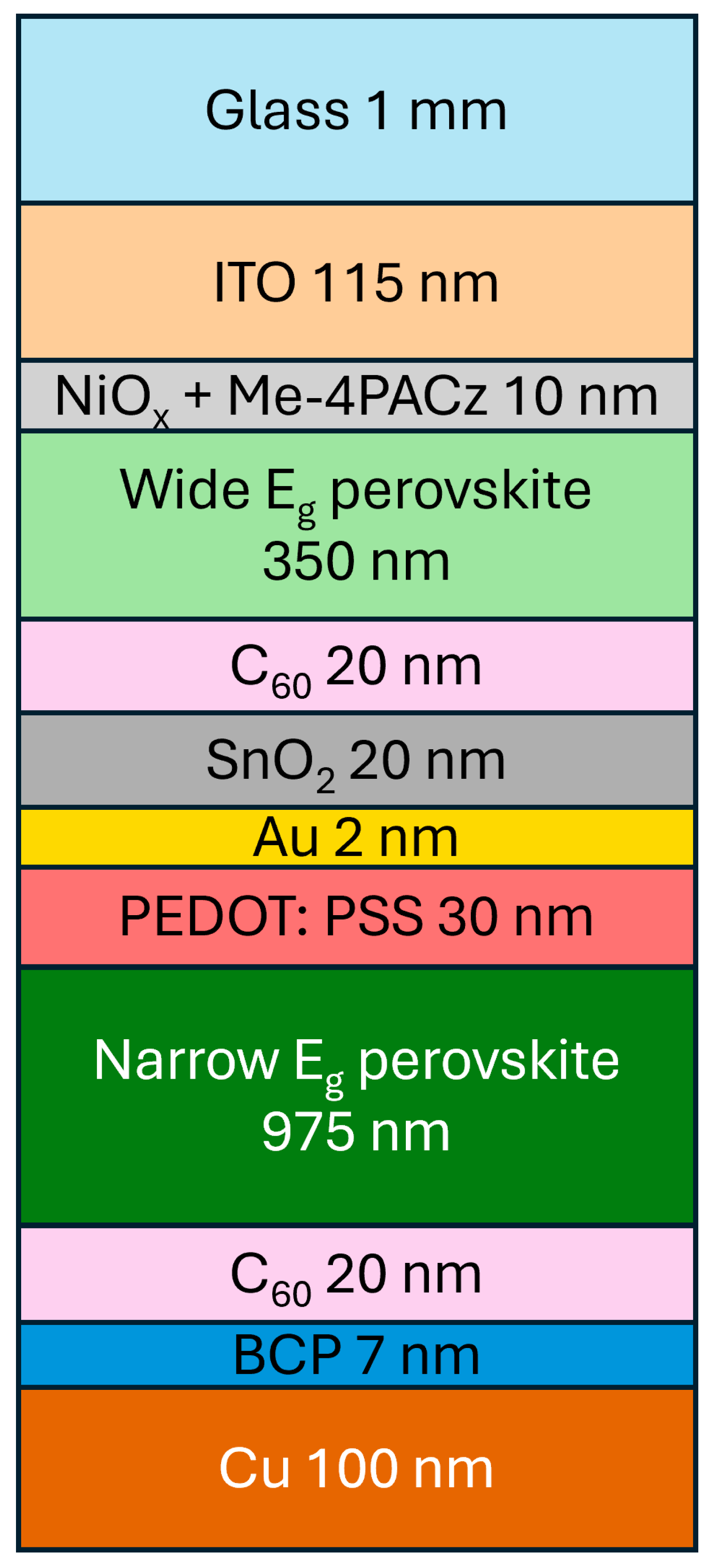
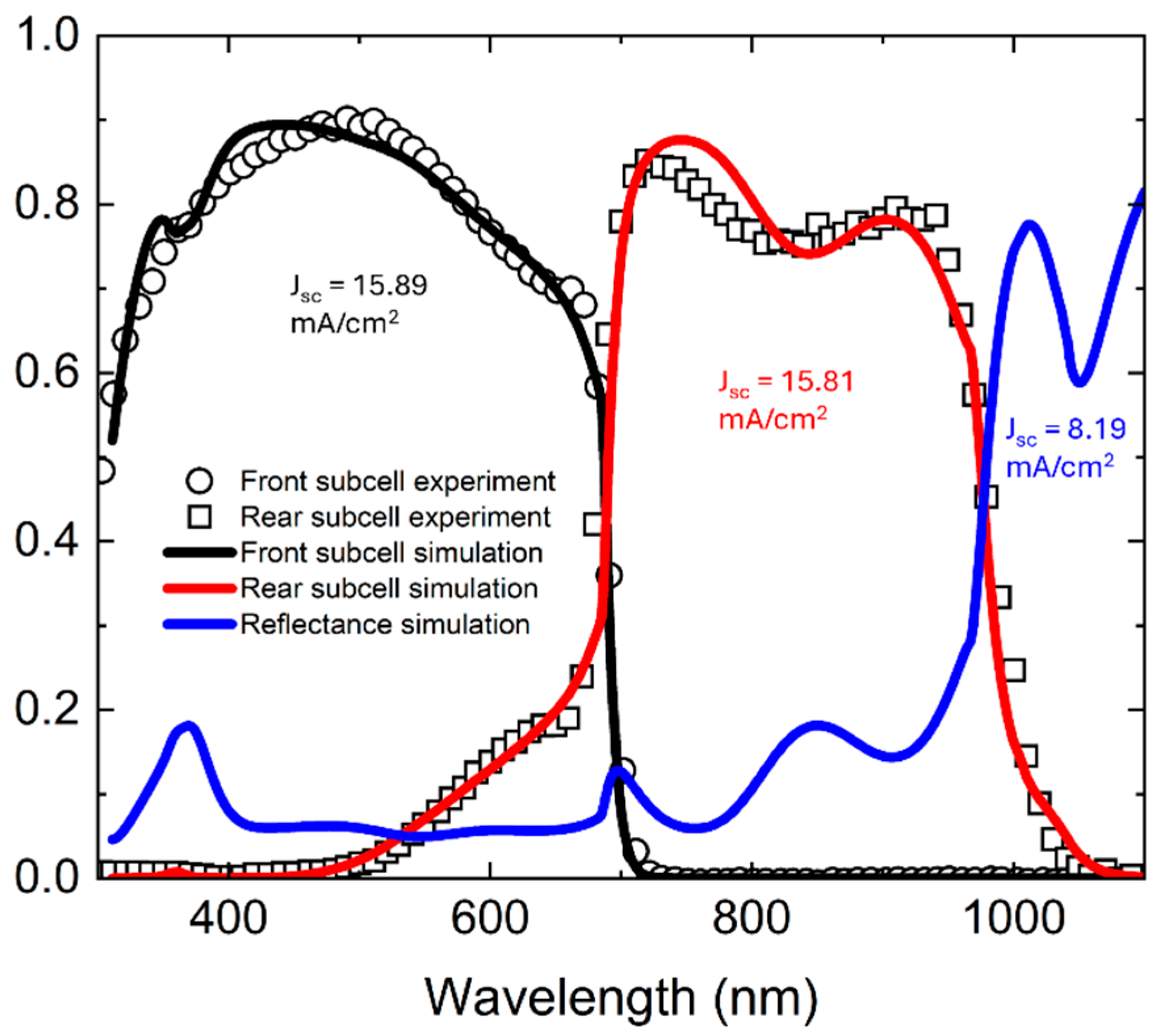
The structural model of the all-perovskite device, shown in Figure 1, consists of 1 mm glass superstrate/115 nm indium-doped tin oxide (ITO)/10 nm effective medium approximation consisting of equal parts ITO and NiOx with a monolayer of Me-4PACz/350 nm wide Eg perovskite where the Eg is 1.8 eV and the Urbach energy is 15 meV/20 nm fullerine (C60)/20 nm of SnO2 deposited by atomic layer deposition/2 nm Au/30 nm PEDOT:PSS/975 nm narrow Eg perovskite where the Eg is 1.29 eV and the Urbach energy is 23 meV/20 nm C60/7 nm bathocuproine/100 nm Cu. The Eg of the wide Eg perovskite is chosen to match what is reported in Wen et al.; the narrow Eg and Urbach energies are chosen to reproduce the shape of the experimental spectrum [3]. The front 25 nm of wide Eg perovskite nearest to the hole transport layer (HTL) is assumed to have a reduced carrier collection probability of 90% to better approximate the experimental spectrum [5,6,7]. These simulated spectra compared with the experimental spectra from Wen et al. are shown in Figure 2 [3]. Layer thicknesses are determined by initially using nominal thicknesses as reported in Wen et al., then adjusting as needed to better approximate the experimental spectrum. Wen et al. report the Au layer as 1 nm thick, but 2 nm Au thicknesses produce better agreement. Nominal thicknesses for the ITO, NiOx, perovskites, and PEDOT:PSS are not reported by Wen et al., so typical thicknesses from the previous literature are chosen and amended to produce agreement with the experimental EQE spectrum [3,8]. Altering these layers’ thicknesses by 5 nm or more produces a noticeable change in the simulated spectrum. A variable thickness MgF2 anti-reflection coating is applied on top of the 1 mm glass superstrate in additional simulations.
Figure 1.
Nominal structural model used to simulate external quantum efficiency (EQE) spectra of an all-perovskite tandem superstrate photovoltaic (PV) device. Thicknesses are chosen to approximate the EQE published by Wen et al. [3].
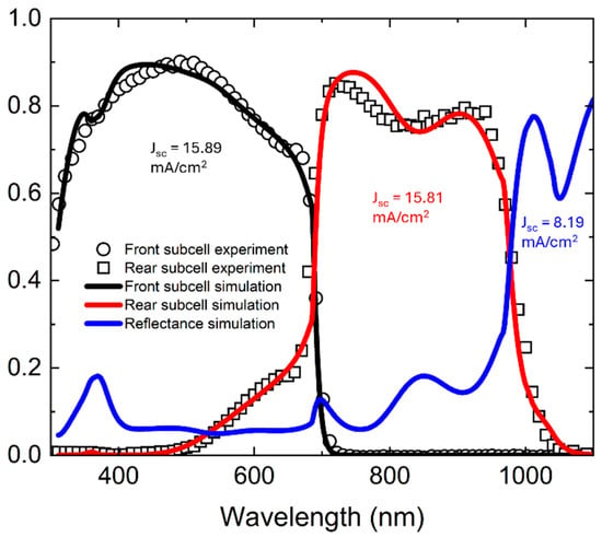
Figure 2.
Simulated EQE (black and red lines) and reflectance (blue line) spectra of an all-perovskite tandem superstrate PV device compared with experimental spectra (symbols) measured by Wen et al. Short circuit current density (Jsc) of each subcell and Jsc loss due to reflectance calculated under AM 1.5 illumination from the simulation are also shown. Jsc for the top and bottom subcells of 15.89 and 15.81 mA/cm2 from simulation are comparable to the experimentally measured Jsc of 15.9 and 16.0 mA/cm2 reported by Wen et al. [3].
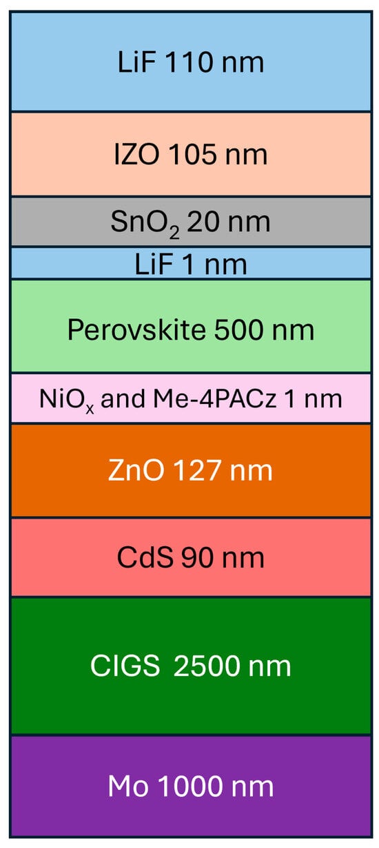
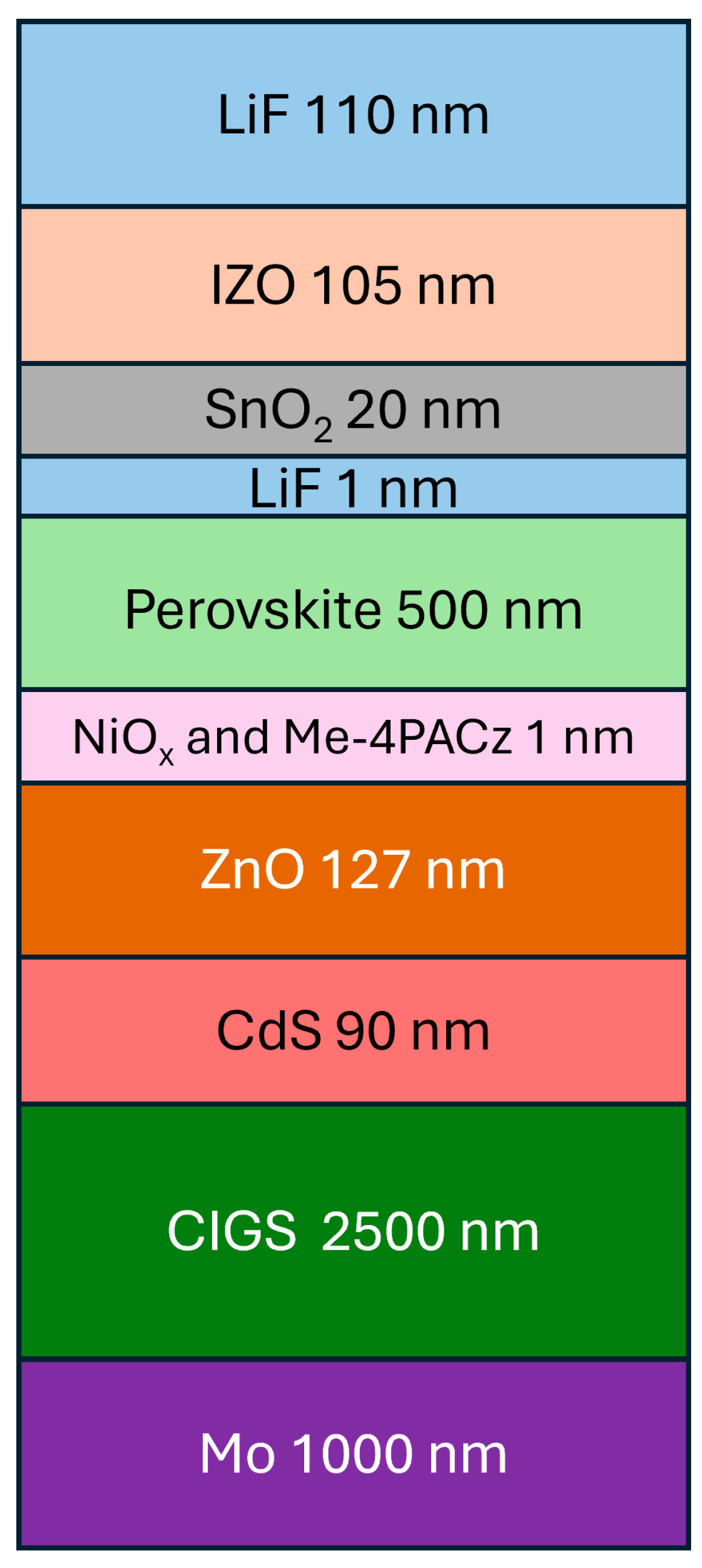
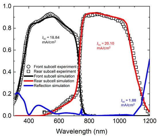
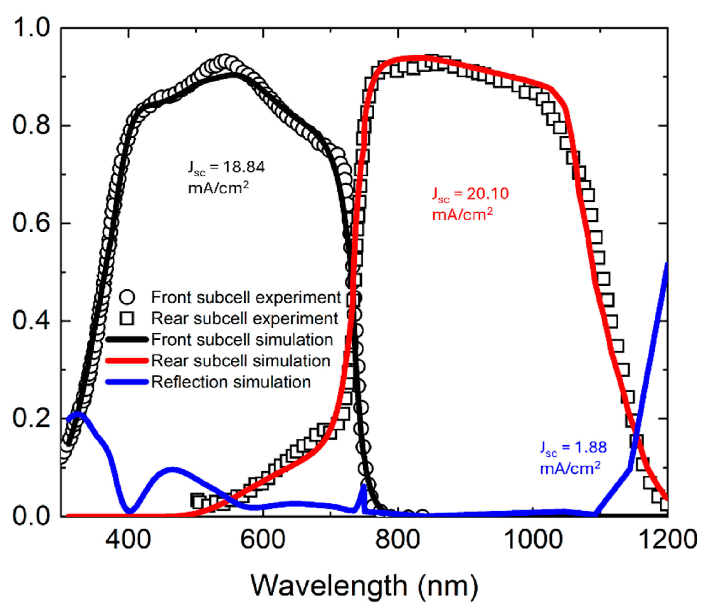
Using results from our previous analyses of perovskite and CIGS solar cells, an initial model is created to approximate the experimental EQE spectra presented by Jošt et al., including optical properties of the perovskite and CIGS absorber layers [3,4,12]. The structural model of the perovskite/CIGS device is shown in Figure 3 and consists of 1 μm molybdenum (Mo) on a soda lime glass substrate/2500 nm CIGS/90 nm cadmium sulfide (CdS)/127 nm zinc oxide (ZnO)/1 nm nickel oxide (NiOx) with a monolayer of Me-4PACz/500 nm perovskite/1 nm lithium fluoride (LiF)/20 nm tin oxide (SnO2)/105 nm indium zinc oxide (IZO)/110 nm LiF. The glass substrate is not shown as the Mo layer is optically opaque over the near-infrared-to-ultraviolet spectral range of PV device operation. The perovskite layer has an Eg of 1.68 eV and an Urbach energy of 25 meV, and the CIGS layer has an Eg of 1.17 eV and an Urbach energy of 34.7 meV. Perovskite Eg is reported in Jost et al., and the Urbach energy is chosen to reproduce the shape of the experimental EQE spectrum. CIGS Eg and Urbach energy are calculated from Aryal et al. assuming x = 0.2 to match the experimental EQE spectrum [12]. The rear 50 nm of perovskite adjacent to the NiOx with Me-4PACz and rear 1000 nm of CIGS adjacent to the Mo are assumed to have reduced carrier collection probabilities of 0%, and the bulk CIGS has reduced carrier collection probability of 90% to better approximate the experimental EQE spectrum. These regions of reduced carrier collection probability coincide with the nucleation layers that occur during thin film growth where more disordered, smaller grained, lower electronic quality material is expected [5,6,7]. Although the modeling approach cannot distinguish explicitly between bulk recombination, interface recombination, and back-contact losses, it does provide the physical locations where electronic losses occur. These simulated spectra compared with the experimental spectra from Jošt et al. are shown in Figure 4 [4].
Figure 3.
Nominal structural model used to simulate EQE spectra of a perovskite/copper indium gallium diselenide (CIGS) tandem substrate PV device. Thicknesses are chosen to approximate the EQE published by Jošt et al. [4].
Figure 4.
Simulated EQE (black and red lines) and reflectance (blue line) spectra of a perovskite/CIGS tandem superstrate PV device compared with experimental spectra (symbols) measured by Jost et al. Jsc of each subcell and Jsc loss due to reflectance calculated under AM 1.5 illumination from the simulation are also shown. Jsc for the top and bottom subcells of 18.84 and 20.10 mA/cm2 from simulation are comparable to the experimentally measured Jsc of 19.0 and 20.0 mA/cm2 reported by Jošt et al. [4].
In additional simulations that vary the absorber layer thicknesses, it is assumed that the regions of reduced carrier collection probabilities maintain the same thicknesses for both tandem device structures. This is a reasonable assumption, as changes in the bulk perovskite thickness are not expected to significantly change the nucleation layer thickness [7].
Optical properties of all simulated materials are obtained from the literature. Perovskite optical properties come from Amonette et al. with revised Eg and Urbach energies, and NiOx plus the Me-4PACz optical properties are also from Amonette et al. [8]. ITO, PEDOT:PSS, BCP and C60 optical properties are published in Subedi et al., and SnO2 optical properties are from Bordovalos et al. [5,6]. Au and Cu optical properties are obtained from the Handbook of Optical Properties of Solids [13]. CIGS optical properties are calculated as described in Aryal et al. assuming x = 0.2 [12]. ZnO optical properties are published in Uprety et al., and CdS optical properties are obtained from Sapkota [14,15]. MgF2 and Mo optical properties come from Hara et al., and LiF optical properties are from Li et al. (1976) [16,17]. CdS optical properties are from Li et al. (2010) [18]. IZO optical properties are obtained from spectroscopic ellipsometry analysis, which is discussed in the Supplementary Materials.
3. Results and Discussion
Jsc is calculated by integrating the product of the EQE spectra with the solar irradiance spectrum with respect to wavelength across the spectral range where substantial absorption occurs in the semiconductor absorber layer. For the all-perovskite tandem device, the calculated Jsc values from simulated EQE spectra under the AM 1.5 solar spectrum are 15.89 mA/cm2 for the wide Eg subcell and 15.81 mA/cm2 for the narrow Eg subcell, which are comparable to Wen et al.’s reported values of 15.9 and 16.0 mA/cm2, respectively [3]. Under the AM 0 irradiance, Jsc in the wide and narrow Eg perovskite subcells are predicted to be 20.21 and 18.65 mA/cm2, respectively. For the CIGS/perovskite tandem device, calculated Jsc from simulated EQE spectra under the AM 1.5 solar spectrum are 18.86 mA/cm2 for the perovskite subcell and 20.37 mA/cm2 for the CIGS subcell, which are comparable to Jošt et al.’s reported values of 19.0 and 20.0 mA/cm2 [4]. Under the AM 0 illumination, Jsc is predicted to be 23.22 mA/cm2 in the perovskite subcell and 23.41 mA/cm2 in the CIGS subcell.
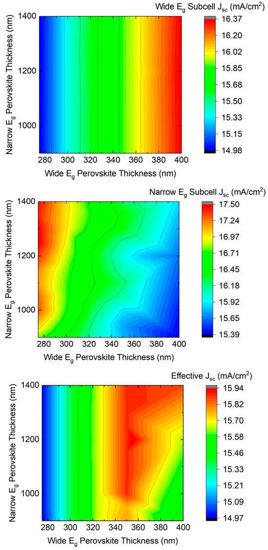
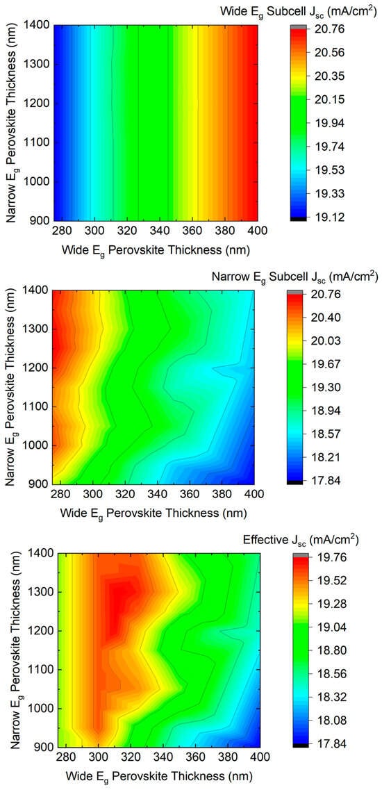
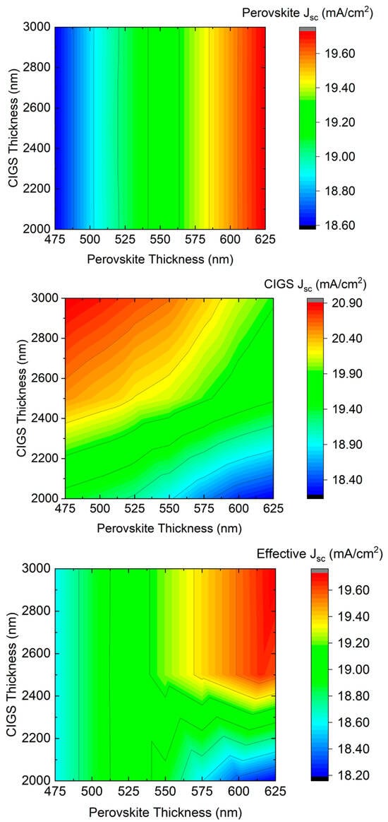
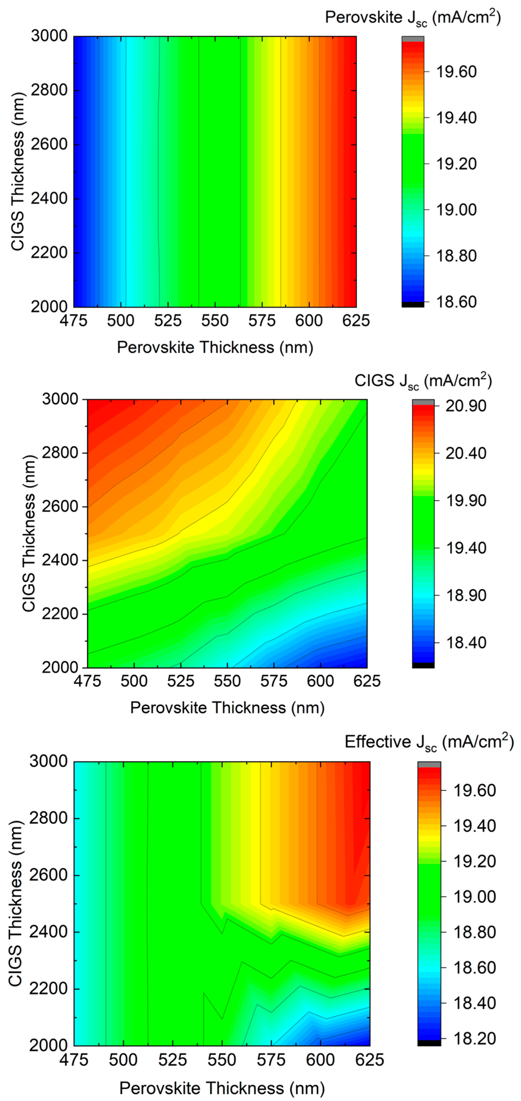
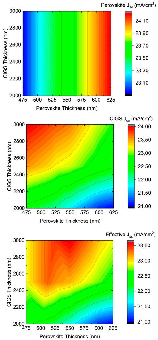
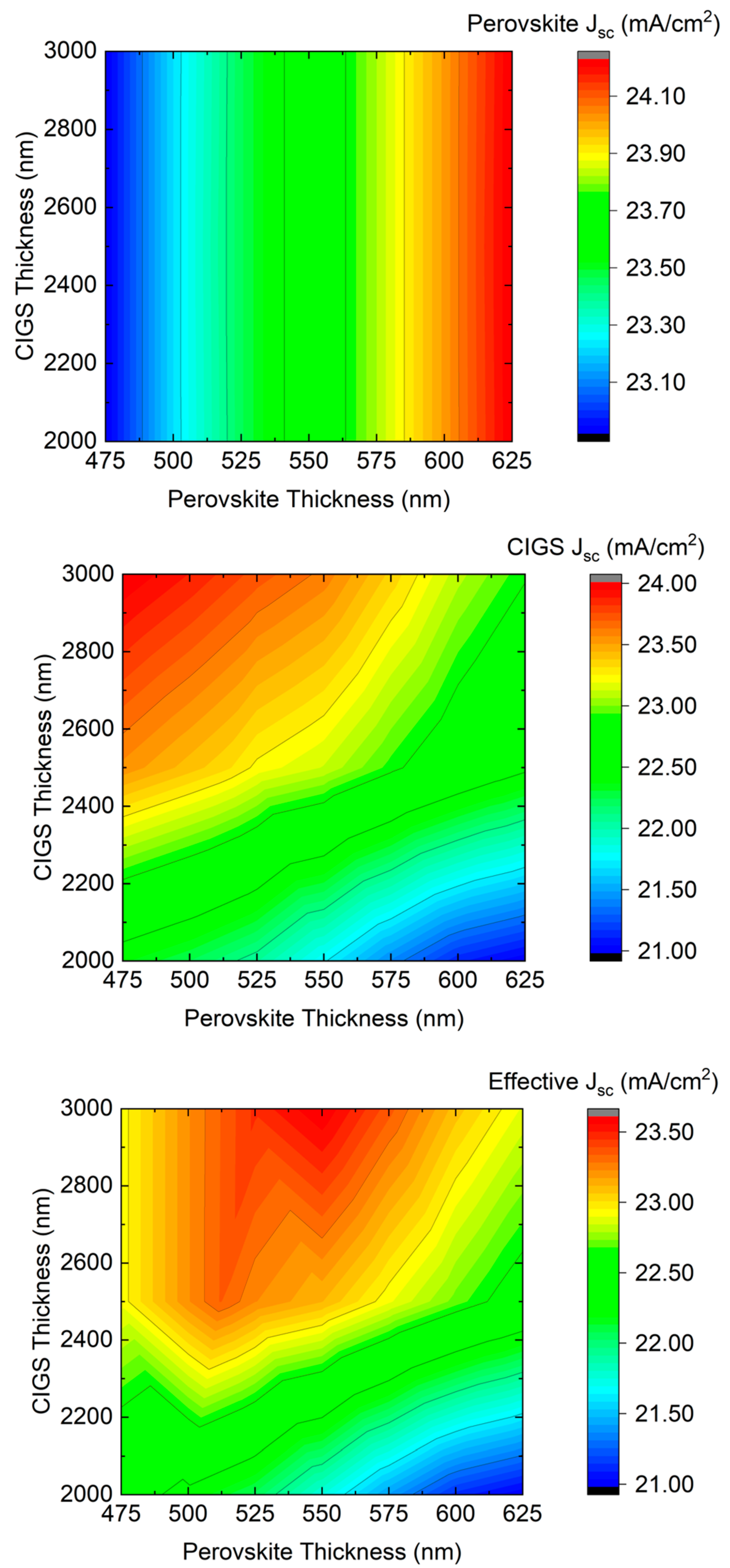
Simulations are repeated with combinations of absorber layer thicknesses with all other parameters fixed to identify practical current matching thicknesses under both AM 1.5 and AM 0 solar irradiance. The resulting Jsc for the all-perovskite device under AM 1.5 irradiance are shown in Figure 5, the all-perovskite device under AM 0 is shown in Figure 6, the perovskite/CIGS device under AM 1.5 is shown in Figure 7, and the perovskite/CIGS device under AM 0 is shown in Figure 8.
Figure 5.
Calculated Jsc under AM 1.5 illumination of the wide Eg and narrow Eg subcells of an all-perovskite tandem device as well as the effective Jsc of the tandem device as functions of absorber layer thicknesses.
Figure 6.
Calculated Jsc under AM 0 illumination of the wide Eg and narrow Eg subcells of an all-perovskite tandem device as well as the effective Jsc of the tandem device as functions of absorber layer thicknesses.
Figure 7.
Calculated Jsc under AM 1.5 illumination of the perovskite and CIGS subcells of a tandem device as well as the effective Jsc of the tandem device as functions of absorber layer thicknesses.
Figure 8.
Calculated Jsc under AM 0 illumination of the perovskite and CIGS subcells of a tandem device as well as the effective Jsc of the tandem device as functions of absorber layer thicknesses.
For the all-perovskite device, narrow Eg perovskite layer thicknesses of up to 1400 nm are simulated, but 1200 nm is chosen as a realistic practical upper limit based on the previous literature [19,20,21]. Tandem device Jsc is limited by the lowest subcell Jsc. Under AM 1.5 illumination, a wide Eg perovskite thickness of 356 nm and narrow Eg perovskite thickness of 1200 nm yields the highest device Jsc of 15.94 mA/cm2, and under AM 0 illumination, a wide Eg perovskite thickness of 310 nm and narrow Eg perovskite thickness of 1200 nm yields the highest device Jsc of 19.72 mA/cm2. Assuming the same Voc and FF as reported in Wen et al., these Jsc values correspond to device efficiencies of 26.05% for the AM 1.5 illumination and 32.22% for the AM 0 illumination. These values are an improvement over the efficiencies calculated using nominal absorber layer thicknesses, which are 25.83% for the AM 1.5 illumination and 30.33% for the AM 0 illumination. The experimentally measured efficiency reported by Wen et al. under AM 1.5 illumination is 26.0%. This is close to the calculated value of 25.83%, and the discrepancy can be attributed to the use of material optical properties already available in the literature rather than the exact optical properties found in the specific device and the structural model applied to describe the device. Regardless of these shortcomings, Jsc are sufficiently close and enable the use of this model to describe the EQE of a high-performance all-perovskite tandem solar cell.
For the perovskite/CIGS device, CIGS layer thicknesses of up to 3000 nm are simulated, but 2500 nm is chosen as a realistic upper limit to CIGS thickness, as Jošt et al. uses a 2500 nm CIGS thickness and CIGS thicknesses exceeding 2500 nm in the literature are uncommon [4]. Under AM 1.5 illumination, a perovskite thickness of 615 nm and CIGS thickness of 2500 nm yields the highest device Jsc of 19.65 mA/cm2, and under AM 0 illumination, a perovskite thickness of 512 nm and CIGS thickness of 2500 nm yields the highest device Jsc of 23.34 mA/cm2. Assuming the same Voc and FF as reported in Jošt et al., these Jsc values correspond to device efficiencies of 24.76% for the AM 1.5 case and 29.41% for the AM 0 case. These values are an improvement over the efficiencies calculated using nominal absorber layer thicknesses, which are 23.74% for the AM 1.5 illumination and 29.15% for the AM 0 illumination. The calculated value under AM 1.5 illumination of 23.74% is comparable to Jošt et al.’s experimentally measured value of 24.2%, and the discrepancy can again be attributed to the use of material optical properties already available in the literature rather than the exact optical properties found in the specific device and the structural model applied to describe the device.
The effects of anti-reflective coating inclusion and thickness for both devices are simulated while absorber thicknesses are kept at their ideal values discussed previously. For the all-perovskite device, optical properties of thin film MgF2 from Hara et al. are used to simulate the anti-reflective coating [16]. The perovskite/CIGS device is simulated with LiF anti-reflective coating in accordance with Jošt et al. [4].
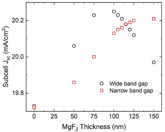
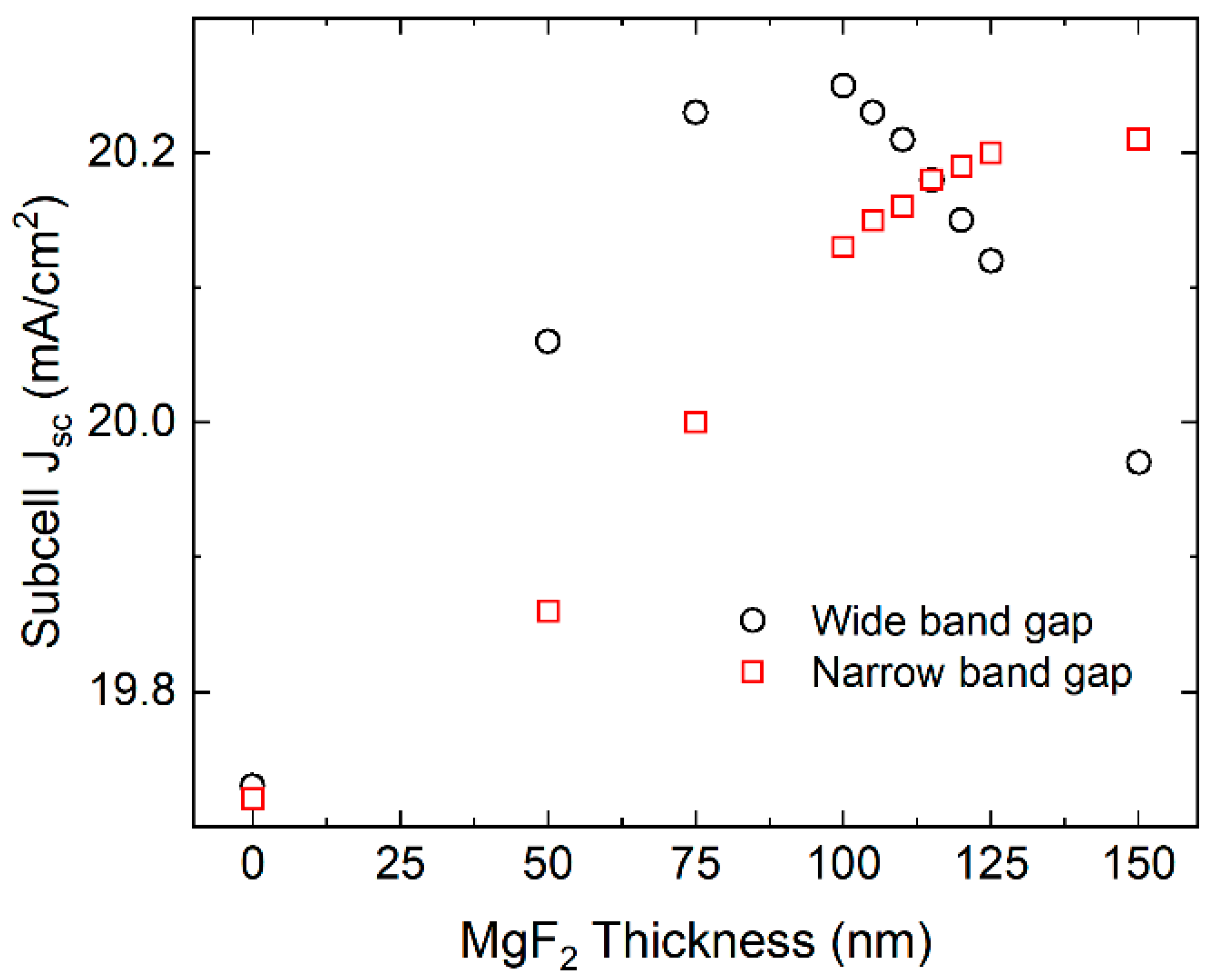
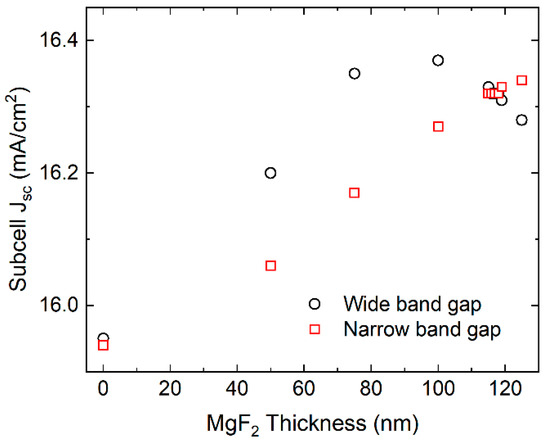
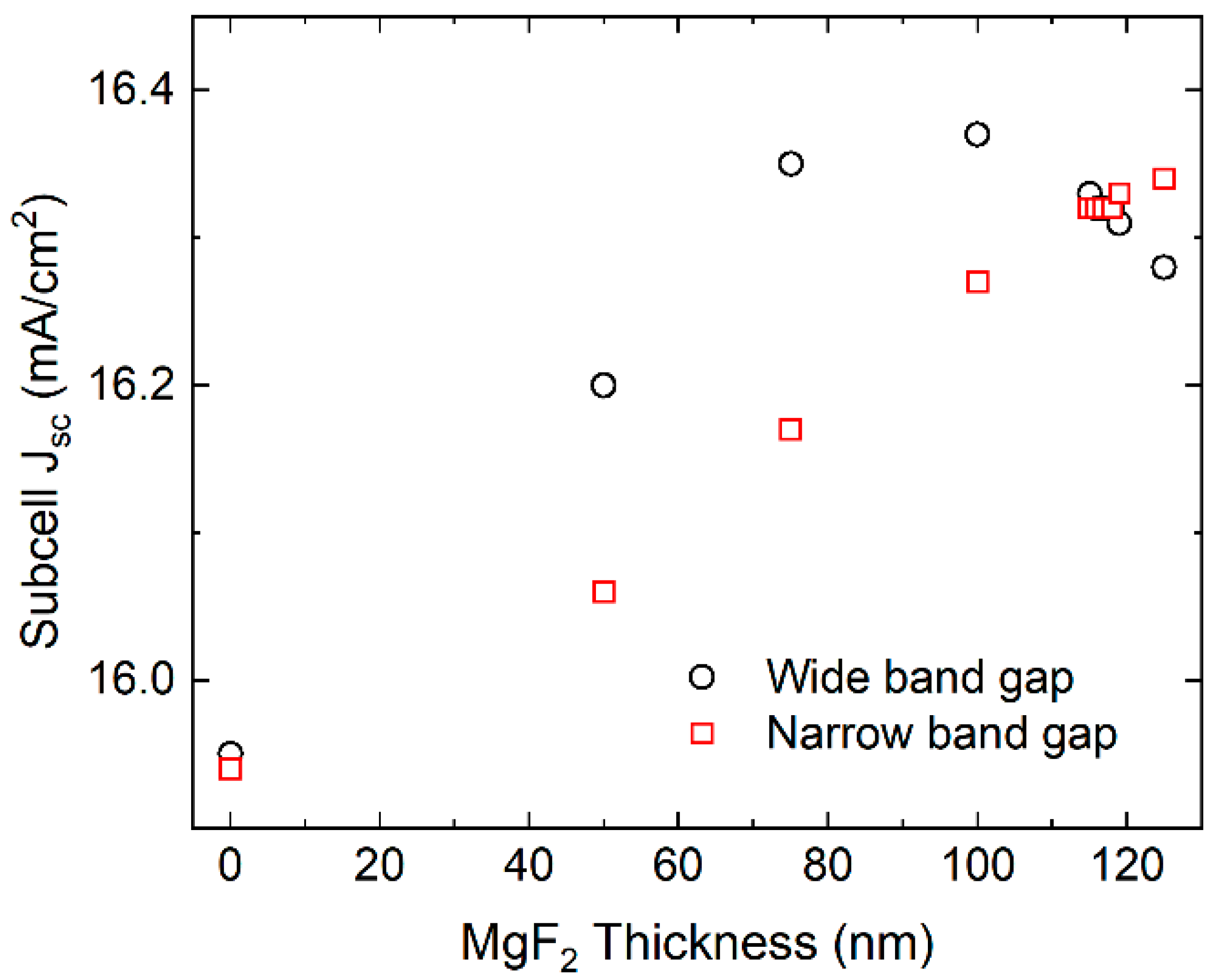
For the all-perovskite device under AM 0 illumination, adding a 115 nm thick MgF2 coating increases the Jsc to 20.18 mA/cm2 as shown in Figure 9 and Table 1, which corresponds to an efficiency of 32.84%, slightly higher than 32.22% without the anti-reflective coating. Under AM 1.5 illumination, a 115–118 nm thick MgF2 anti-reflective coating on top of the glass superstrate increases the Jsc to 16.32 mA/cm2 as shown in Figure 10 and Table 2 which corresponds to an efficiency of 26.67%, again slightly higher than 26.05% without anti-reflective coating. Although these increases in Jsc are greater than the error between the experimental and simulated values, this small increase in Jsc is likely not substantial. It is also prudent to consider that small variations in performance parameters can exist across nominally identical devices [9]. However, these calculations reveal the trend that occurs with increasing MgF2 thickness in this device structure.
Figure 9.
Calculated Jsc as a function of MgF2 anti-reflection coating film thickness of wide and narrow Eg subcells of an all-perovskite tandem PV device where the wide Eg perovskite is 310 nm thick and the narrow Eg perovskite is 1200 nm thick under AM 0 illumination. The narrow Eg thickness is chosen as this is the thickest perovskite absorber layer in a tandem device reported in the literature, and the wide Eg thickness is chosen to produce current matching conditions under AM 0 illumination.
Table 1.
Calculated Jsc as a function of MgF2 anti-reflection coating film thickness of wide and narrow Eg subcells of an all-perovskite tandem PV device as well as Jsc loss to reflection where the wide Eg perovskite is 310 nm thick and the narrow Eg is 1200 nm under AM 0 illumination. The narrow Eg thickness is chosen as this is the thickest perovskite absorber layer thickness in a tandem device seen in the literature, and the wide Eg thickness is chosen to produce current matching conditions under AM 0 illumination.
Figure 10.
Calculated Jsc as a function of MgF2 anti-reflection coating film thickness of wide and narrow Eg subcells of an all-perovskite tandem PV device where the wide Eg perovskite is 356 nm thick and the narrow Eg perovskite is 1200 nm thick under AM 1.5 illumination. The narrow Eg thickness is chosen as this is the thickest perovskite absorber layer in a tandem device reported in the literature, and the wide Eg thickness is chosen to produce current matching conditions under AM 1.5 illumination.
Table 2.
Calculated Jsc as a function of MgF2 anti-reflection coating film thickness of wide and narrow Eg subcells of an all-perovskite tandem PV device as well as Jsc loss to reflection where the wide Eg perovskite is 356 nm thick and the narrow Eg is 1200 nm under AM 1.5 illumination. The narrow Eg thickness is chosen as this is the thickest perovskite absorber layer thickness in a tandem device seen in the literature, and the wide Eg thickness is chosen to produce current matching conditions under AM 1.5 illumination.
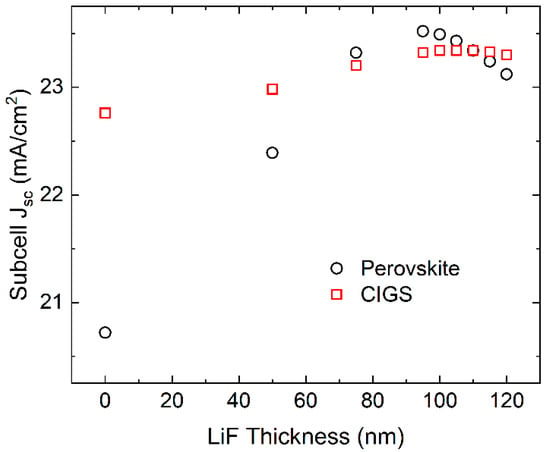
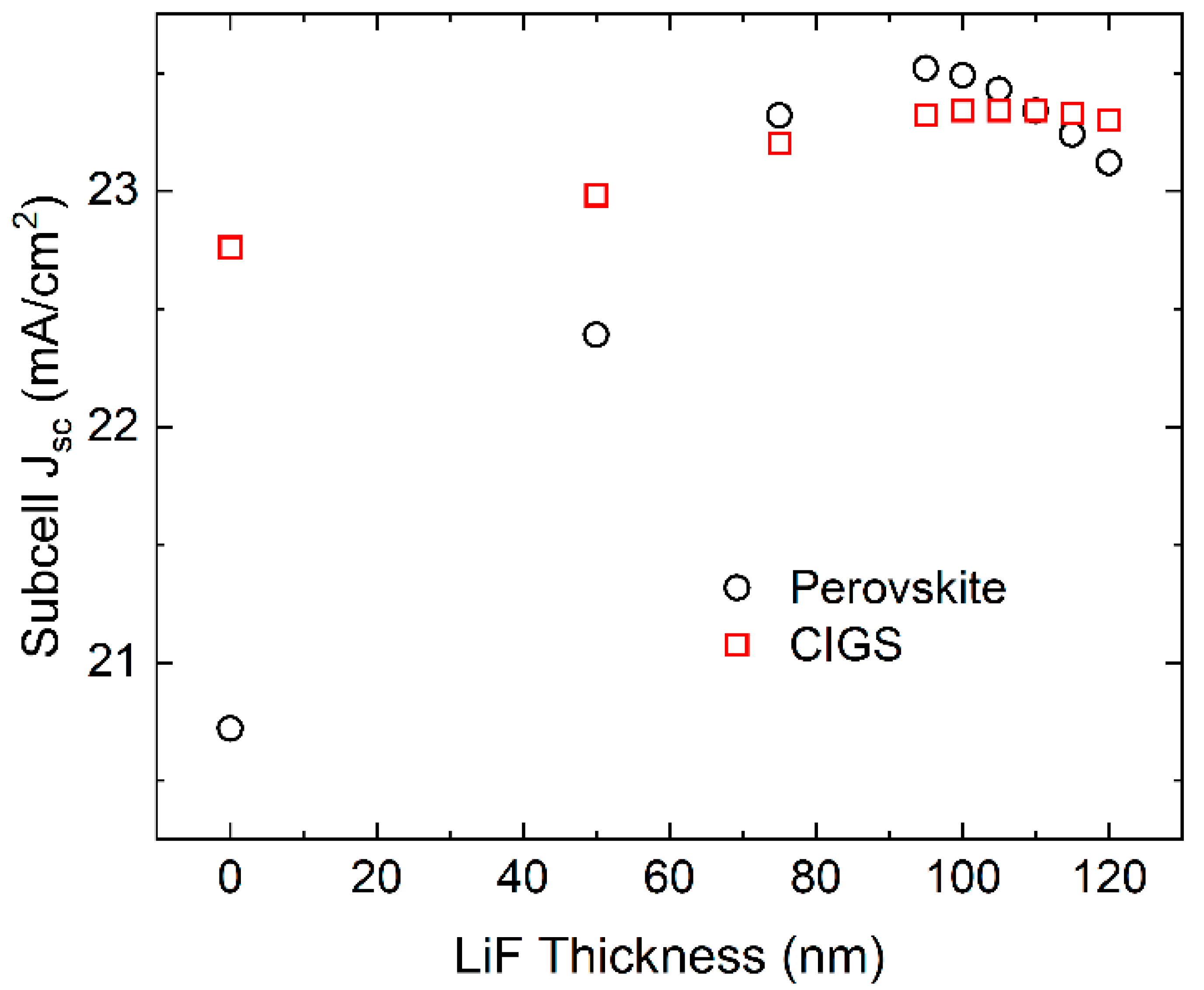
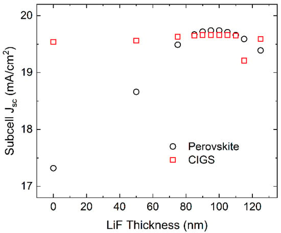
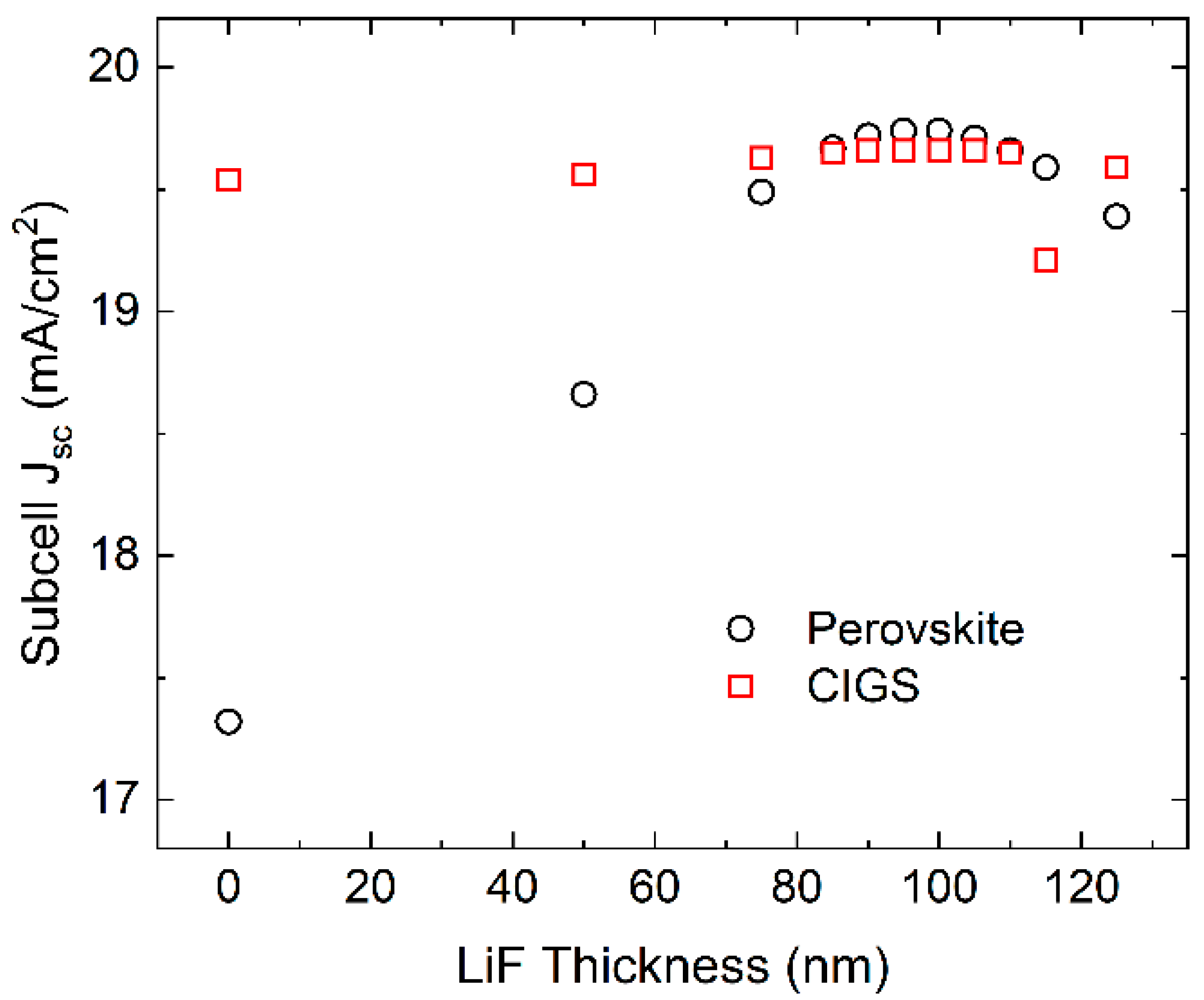
The perovskite/CIGS device is simulated with a 110 nm thick LiF anti-reflective coating as in Jošt et al. [4]. Under AM 0 illumination, this is the ideal LiF thickness to use with the absorber layer thicknesses here as shown in Figure 11 and Table 3, although any LiF thickness between 100 and 110 nm yields the same effective Jsc. Under AM 1.5 illumination, although approximate current matching occurs at 110 nm LiF, a slightly higher effective Jsc can be achieved when the LiF thickness is between 90 and 105 nm as shown in Figure 12 and Table 4. Assuming the same values for Voc and FF as reported in Jošt et al., the efficiency at 110 nm LiF would be 24.76% while LiF thickness between 90 and 105 nm would yield 24.78% efficiency.
Figure 11.
Calculated Jsc as a function of LiF anti-reflection coating film thickness of perovskite and CIGS subcells in a tandem PV device where the perovskite is 512 nm thick and the CIGS layer is 2500 nm thick under AM 0 illumination. The CIGS thickness is chosen to match the literature, and the perovskite thickness is chosen to produce current matching conditions under AM 0 illumination.
Table 3.
Calculated Jsc as a function of LiF anti-reflection coating film thickness of perovskite and CIGS subcells in a tandem PV device as well as Jsc loss to reflection where the perovskite is 512 nm thick and the CIGS layer is 2500 nm thick under AM 0 illumination. The CIGS layer thickness is chosen to match the literature, and the perovskite thickness is chosen to produce current matching conditions under AM 0 illumination.
Figure 12.
Calculated Jsc as a function of LiF anti-reflection coating film thickness of perovskite and CIGS subcells in a tandem PV device where the perovskite is 615 nm thick and the CIGS layer is 2500 nm thick under AM 1.5 illumination. The CIGS thickness is chosen to match the literature, and the perovskite thickness is chosen to produce current matching conditions under AM 1.5 illumination.
Table 4.
Calculated Jsc as a function of LiF anti-reflection coating film thickness of perovskite and CIGS subcells in a tandem PV device as well as Jsc loss to reflection where the perovskite is 615 nm thick and the CIGS layer is 2500 nm thick under AM 1.5 illumination. The CIGS layer thickness to match the literature, and the perovskite thickness is chosen to produce current matching conditions under AM 1.5 illumination.
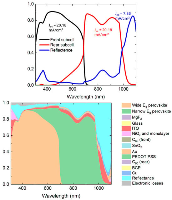
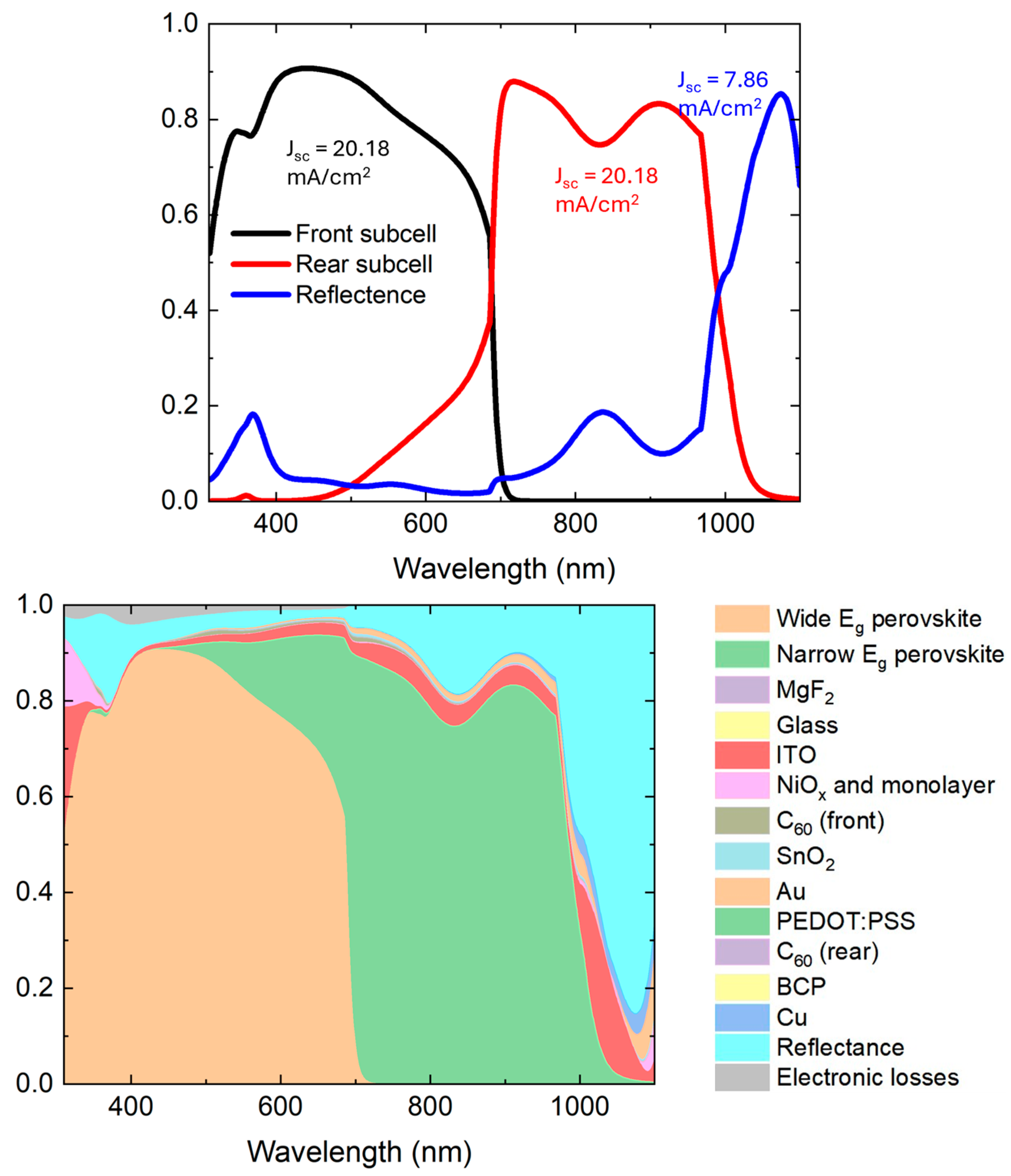
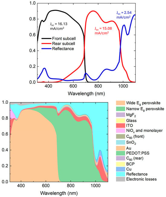
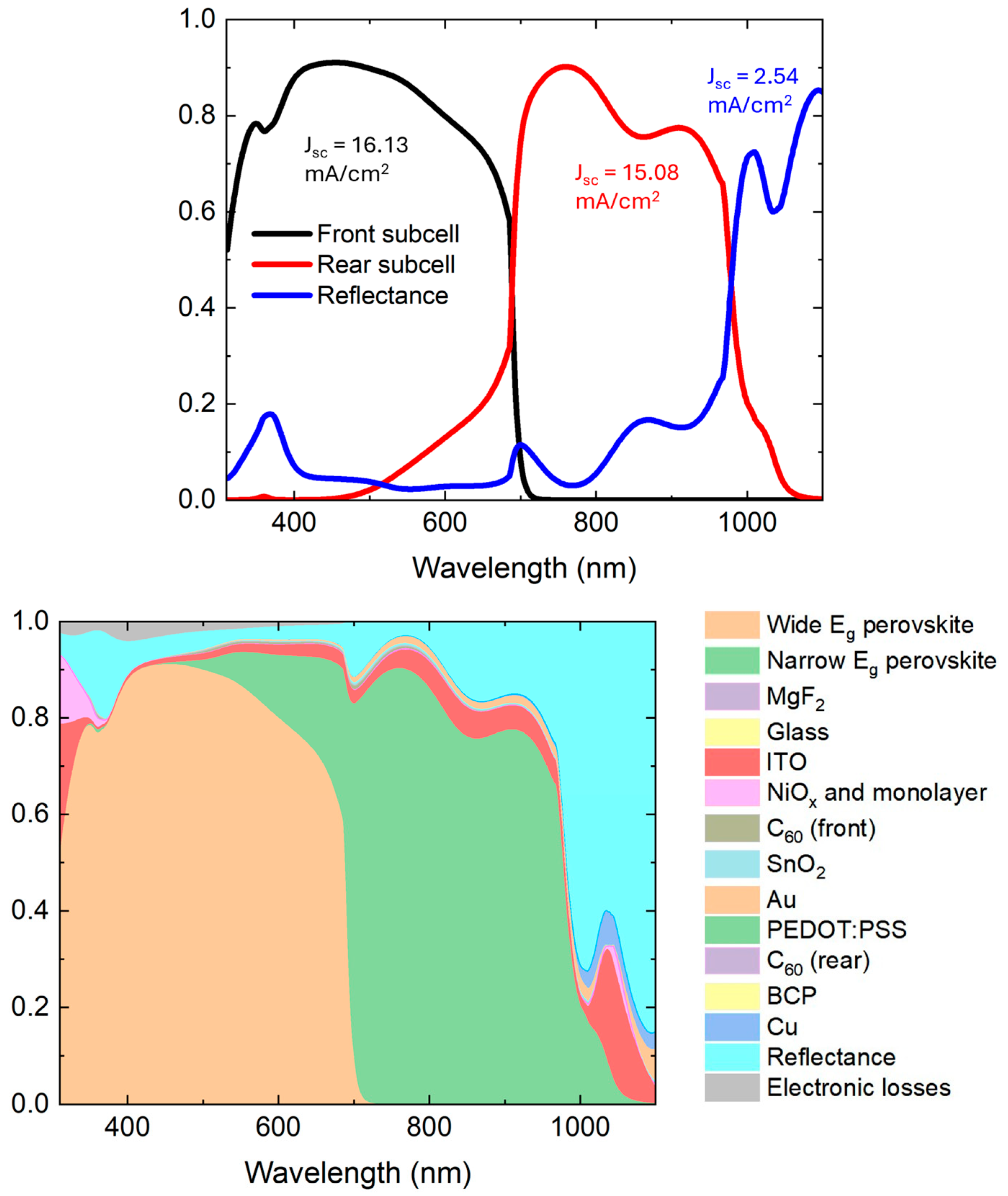
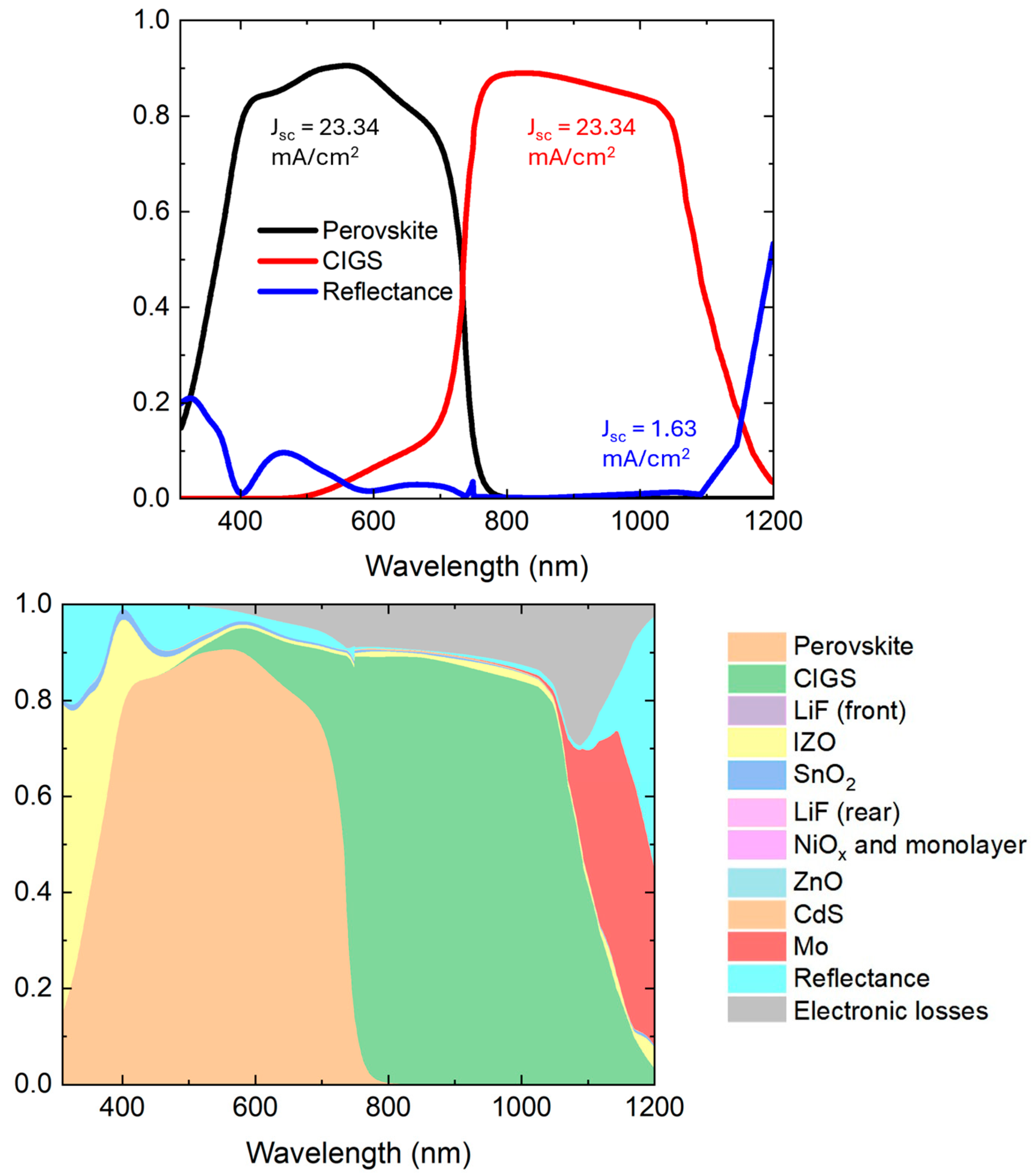
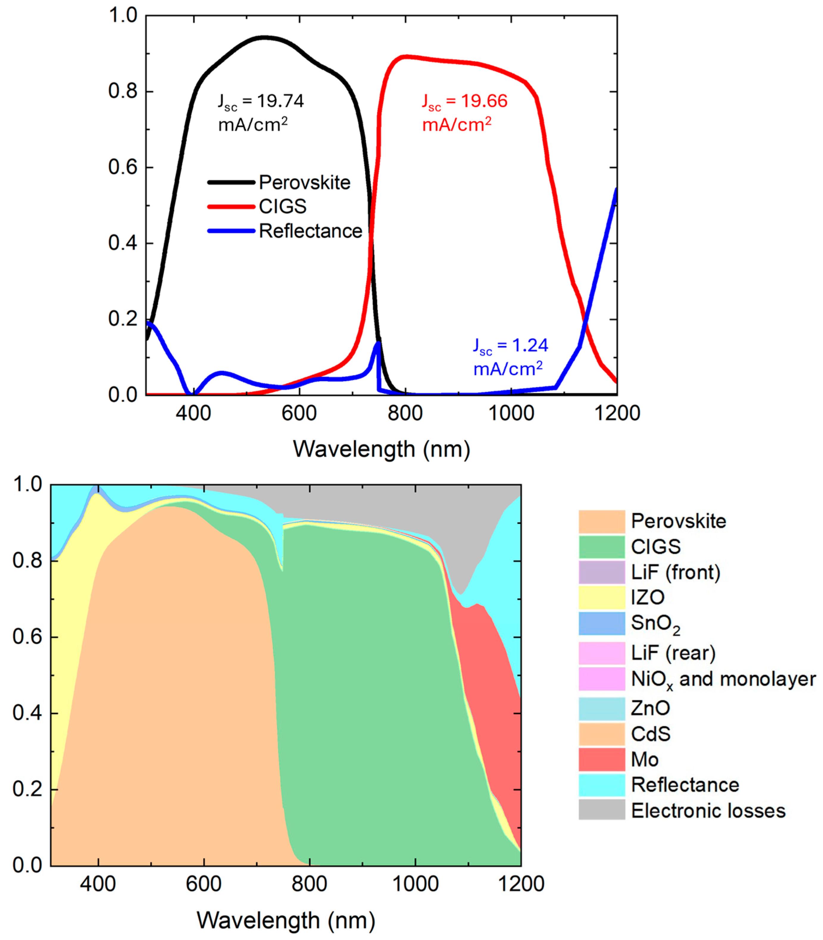
Further simulations of each device using optimized absorber layer and anti-reflective coating layer thicknesses are performed and the EQE spectra, absorption spectra of each layer, reflectance, illuminance, and electronic losses are determined to serve as a basis for further Jsc optimization. Results for the all-perovskite device under AM 0 illumination are shown in Figure 13 and Table 5, results for the all-perovskite device under AM 1.5 illumination are shown in Figure 14 and Table 6, results for the CIGS/perovskite device under AM 0 are shown in Figure 15 and Table 7, and results for the CIGS/perovskite device under AM 1.5 are shown in Figure 16 and Table 8. These results serve as a starting point for further optimization. For example, in the all-perovskite devices, there is substantial reflection loss equivalent to 9.18 mA/cm2 of lost current for the device under AM 1.5 illumination and 7.86 mA/cm2 for the device under AM 0 illumination despite the simulated anti-reflective coating. Application of different anti-reflective materials, multilayer coatings, or texturing could improve device performance [22,23]. Additionally, the ITO exhibits the highest parasitic absorption of any layer in the device equivalent to a current loss of 2.48 mA/cm2 for the device under AM 1.5 illumination and 2.70 mA/cm2 for the device under AM 0 illumination; altering its thickness or replacing it with another transparent conducting oxide could also improve device performance [24,25]. The NiOx and monolayer of Me4-PACz also exhibits substantial parasitic absorption at short wavelengths which limits the Jsc from the wide Eg perovskite top subcells, and either its modification or replacement could be a subject of future research [26]. The CIGS/perovskite device exhibits significant electronic losses of 4.17 mA/cm2 in the AM 0 case and 3.44 mA/cm2 in the AM 1.5 case which could be reduced by improving the quality of the CIGS layer [27,28,29]. The IZO layer also exhibits parasitic absorption at short wavelengths, which could be minimized by altering its thickness or replacing it with another transparent conducting oxide [24,25].
Figure 13.
Simulated EQE and reflection spectra of the optimized all-perovskite tandem PV device under AM 0 illumination (top) and absorbance of each layer of the device as well as reflectance and electronic losses (bottom). The optimized device is simulated as having 115 nm MgF2 anti-reflective coating, 310 nm thick wide Eg perovskite, and 1200 nm thick narrow Eg perovskite.
Table 5.
Equivalent Jsc losses from parasitic absorption in each device component layer of the optimized all-perovskite tandem PV device under AM 0 illumination, as well as contribution from reflectance and electronic losses.
Figure 14.
Simulated EQE and reflection spectra of the optimized all-perovskite tandem PV device under AM 1.5 illumination (top) and absorbance of each layer of the device as well as reflectance and electronic losses (bottom). The optimized device is simulated as having 117 nm MgF2 anti-reflective coating, 356 nm thick wide Eg perovskite, and 1200 nm thick narrow Eg perovskite.
Table 6.
Equivalent Jsc losses from parasitic absorption in each device component layer of the optimized all-perovskite tandem PV device under AM 1.5 illumination, as well as contribution from reflectance and electronic losses.
Figure 15.
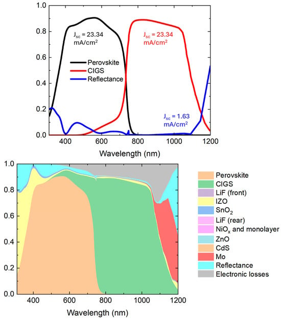
Simulated EQE and reflection spectra of the optimized CIGS/perovskite tandem PV device under AM 0 illumination (top) and absorbance of each layer of the device as well as reflectance and electronic losses (bottom). The optimized device is simulated as having 110 nm LiF anti-reflective coating, 512 nm thick perovskite, and 2500 nm thick CIGS.
Table 7.
Equivalent Jsc losses from parasitic absorption in each device component layer of the optimized CIGS/perovskite tandem PV device under AM 0 illumination, as well as contribution from reflectance and electronic losses.
Figure 16.
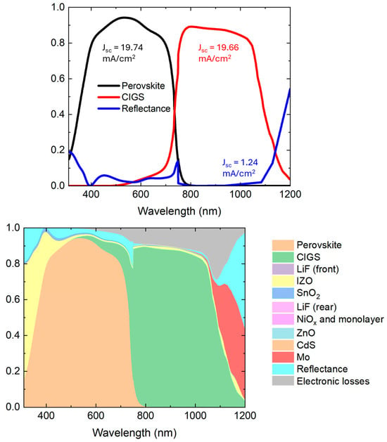
Simulated EQE and reflection spectra of the optimized CIGS/perovskite tandem PV device under AM 1.5 illumination (top) and absorbance of each layer of the device as well as reflectance and electronic losses (bottom). The optimized device is simulated as having 95 nm LiF anti-reflective coating, 615 nm thick perovskite, and 2500 nm thick CIGS.
Table 8.
Equivalent Jsc losses from parasitic absorption in each device component layer of the optimized CIGS/perovskite tandem PV device under AM 1.5 illumination, as well as contribution from reflectance and electronic losses.
There are limitations to this methodology of using transfer matrix-based EQE simulations to model PV device Jsc and performance. These simulations do not directly calculate other key PV performance factors such as open circuit voltage and fill factor. Additionally, these simulations are purely based on optical calculations and do not account for parameters seen in real devices the way other simulation software such as SCAPS 1-D 3.3.10 might. In addition to complex dielectric function spectra, SCAPS 1-D can account for defect densities, carrier mobilities, resistances and more, though when calculating Jsc, optical-based simulation software such as e-ARC produces results closer to experiment [8]. The optical properties used as input for each material in the simulations in this manuscript are obtained from available published spectra, so they may not perfectly represent the properties of the experimental device. The PCE calculations performed in this manuscript assume no changes in the Voc and FF when altering thickness parameters, but in reality there may be changes in these values that would also affect PCE [8]. These changes are more pronounced in subcells with thicker absorber layers, such as narrow Eg perovskites and CIGS [30,31]. Device performance simulations are unable to account for every nonideality that occurs in actual devices; however, the general trends revealed by these calculations are useful in informing future experimental work. If such theoretically optimized devices were fabricated, their simulated performance parameters could be compared with experimental results, and device layer thicknesses and material complex optical properties could be obtained from a method such as spectroscopic ellipsometry to further corroborate or enhance the accuracy of simulations [9].
4. Conclusions
Optical models of complete superstrate and substrate tandem solar cells have been developed to generate practical models of previously published EQE spectra based on measured complex optical property spectra of component materials for the purpose of further Jsc optimization. These models can be used to easily simulate the effects of altering layer thicknesses and adding anti-reflective layers and evaluation of losses in current solar cell designs. These models also enable us to study the effects of using alternative materials to replace various layers of the device as long as the complex optical response of those materials have been measured. In this way, models replicating the structure of real high-efficiency devices can be used to evaluate practical performance gains from different device structure optimizations.
The performance of tandem perovskite PV devices such as the ones fabricated by Wen et al. and Jošt et al. can be improved by adjusting absorber layer thicknesses, and EQE simulations are a useful tool for optimizing these thicknesses under different illuminations. When optimizing PV devices for space-based applications, the difference in Jsc under AM 0 illumination is an important consideration, as the ideal thickness combination may not be the same as that of an optimized terrestrial device under AM 1.5 illumination.
For the all-perovskite tandem device, by increasing the thicknesses of the wide Eg and narrow Eg perovskite absorber layers from 350 and 975 nm to 356 and 1200 nm, the Jsc may be increased from 15.81 to 15.94 mA/cm2 under AM 1.5 illumination. This corresponds to an increase in efficiency from 25.83 to 26.05%. Additionally, adding a 115–118 nm thick MgF2 anti-reflective layer may further increase Jsc to 16.32 mA/cm2, corresponding to an efficiency of 26.67%. Under AM 0, a change in absorber layer thicknesses to 310 and 1200 nm increases the Jsc from 18.56 to 19.72 mA/cm2, which corresponds to an increase in efficiency from 30.33 to 32.22%. By adding 115 nm MgF2, the Jsc may be further increased to 20.18 mA/cm2, increasing the efficiency to 32.84%.
For the perovskite/CIGS device, by increasing the thicknesses of the perovskite layer from 500 to 615 nm, the Jsc may be increased from 18.84 to 19.65 mA/cm2 under AM 1.5 illumination. Assuming the same values for Voc and FF as reported by Jošt et al., this means the efficiency would increase from 23.74 to 24.76%. Under AM 0 illumination, an increase in the perovskite thickness to 512 nm results in an increase in predicted Jsc from 23.13 to 23.34 mA/cm2. This corresponds to a predicted efficiency increase from 29.15 to 29.41%.
Absorption, reflection, and electronic losses affect the performance of each layer, and these losses serve as a starting point for further optimization. For example, in the all-perovskite devices, there is significant reflection loss despite the simulated anti-reflective coating. Application of different anti-reflective materials, multilayer coatings, or texturing could improve device performance. Additionally, the ITO exhibits the highest parasitic absorption of any layer in the device; altering its thickness or replacing it with another transparent conductor could also improve device performance. The NiOx and Me4-PACz monolayer also exhibits substantial parasitic absorption at short wavelengths which limits the Jsc from the wide Eg perovskite top subcells and could be a subject of future research. The CIGS/perovskite device exhibits significant electronic losses which could be reduced by improving the quality of the CIGS layer. The IZO layer also exhibits parasitic absorption at short wavelengths, which could be minimized by altering its thickness or replacing it with another transparent conducting oxide. For space-based applications, there are further considerations not accounted for in this methodology, such as high-energy radiation, thermal cycling and micrometeorite impacts [32]. Overall, the models developed for these two tandem device configurations, benchmarked against experimental high-efficiency devices, serve as a framework to investigate other variations in device structure and material characteristics. This helps to establish realistic practical expectations prior to more costly and time-consuming device fabrication processes.
Supplementary Materials
The following supporting information can be downloaded at: https://www.mdpi.com/article/10.3390/ma19173618/s1. References [33,34,35,36,37,38,39,40,41] are cited in the Supplementary Materials.
Author Contributions
Conceptualization, N.J.P.; methodology, E.A. and N.J.P.; formal analysis, E.A.; resources, N.J.P.; writing—original draft preparation, E.A.; writing—review and editing, E.A. and N.J.P.; supervision, N.J.P.; funding acquisition, N.J.P. All authors have read and agreed to the published version of the manuscript.
Funding
This material is based on research sponsored by Air Force Research Laboratory under agreement number FA9453-21-C-0056. The U.S. Government is authorized to reproduce and distribute reprints for Governmental purposes notwithstanding any copyright notation thereon. The views expressed are those of the authors and do not reflect the official guidance or position of the United States Government, the Department of Defense or of the United States Air Force. The appearance of external hyperlinks does not constitute endorsement by the United States Department of Defense (DoD) of the linked websites, or the information, products, or services contained therein. The DoD does not exercise any editorial, security, or other control over the information you may find at these locations. Approved for public release; distribution is unlimited. Public Affairs release approval #AFRL-2025-3790.
Data Availability Statement
The original contributions presented in this study are included in the article/Supplementary Materials. Further inquiries can be directed to the corresponding author.
Acknowledgments
The content of this article is based on the author’s Ph.D thesis and is authorized by the University of Toledo for further publication. The source is Analysis of Thin Films, Bulk Materials, and Devices via Spectroscopic Ellipsometry by Emily Jo Amonette at the University of Toledo, Toledo, Ohio, United States, 2025.
Conflicts of Interest
The authors declare no conflicts of interest.
References
- Dong, H.; Ran, C.; Gao, W.; Li, M.; Xia, Y.; Huang, W. Metal Halide Perovskite for next-generation optoelectronics: Progresses and prospects. eLight 2023, 3, 3. [Google Scholar] [CrossRef] [Scilit]
- NREL, Best Research-Cell Efficiencies. Available online: https://www.nlr.gov/media/docs/libraries/pv/cell-pv-eff.pdf (accessed on 3 February 2025).
- Wen, J.; Zhao, Y.; Liu, Z.; Gao, H.; Lin, R.; Wan, S.; Ji, C.; Xiao, K.; Gao, Y.; Tian, Y.; et al. Steric Engineering Enables Efficient and Photostable Wide-Bandgap Perovskites for All-Perovskite Tandem Solar Cells. Adv. Mater. 2022, 34, 2100356. [Google Scholar] [CrossRef] [Scilit]
- Jošt, M.; Köhnen, E.; Al-Ashouri, A.; Bertram, T.; Tomšič, S.; Magomedov, A.; Kasparavicius, E.; Kodalle, T.; Lipovšek, B.; Getautis, V.; et al. Perovskite/CIGS Tandem Solar Cells: From Certified 24.2% toward 30% and Beyond. ACS Energy Lett. 2022, 7, 4. [Google Scholar] [CrossRef] [Scilit]
- Subedi, B.; Song, Z.; Chen, C.; Li, C.; Ghimire, K.; Junda, M.M.; Subedi, I.; Yan, Y.; Podraza, N.J. Optical and Electronic Losses Arising from Physically Mixed Interfacial Layers in Perovskite Solar Cells. ACS Appl. Mater. Interfaces 2021, 13, 4923. [Google Scholar] [CrossRef] [Scilit]
- Bordovalos, A.; Subedi, B.; Chen, L.; Song, Z.; Yan, Y.; Podraza, N.J. Implications of Electron Transport Layer and Back Metal Contact Variations in Tin-Lead Perovskite Solar Cells assessed by Spectroscopic Ellipsometry and External Quantum Efficiency. ACS Appl. Mater. Interfaces 2023, 15, 19730–19740. [Google Scholar] [CrossRef] [Scilit]
- Tumusange, M.S.; Chen, L.; Mainali, M.K.; Frye, B.M.; Amonette, E.J.; Bordovalos, A.V.; Song, Z.; Yan, Y.; Podraza, N.J. Monitoring degradation and carrier collection losses of narrow bandgap perovskite solar cells with different organic hole transport layers by spectroscopic ellipsometry and external quantum efficiency. Sol. Energy 2025, 288, 113243. [Google Scholar] [CrossRef] [Scilit]
- Amonette, E.; Dolia, K.; Yan, Y.; Song, Z.; Podraza, N.J. Predicting Perovskite Photovoltaics Performance. ACS Appl. Mater. Interfaces 2025, 17, 10014–10026. [Google Scholar]
- Nakane, A.; Tampo, H.; Tamakoshi, M.; Fujimoto, S.; Min Kim, K.; Kim, S.; Shibata, H.; Niki, S.; Fujiwara, H. Quantitative determination of optical and recombination losses in thin-film photovoltaic devices based on external quantum efficiency analysis. J. Appl. Phys. 2016, 120, 064505. [Google Scholar] [CrossRef] [Scilit]
- Subedi, I.; Silverman, T.J.; Deceglie, M.; Podraza, N.J. Al+Si Interface Optical Properties obtained in the Si Solar Cell Configuration. Phys. Status Solidi A 2017, 214, 1700480. [Google Scholar] [CrossRef] [Scilit]
- Schlenker, T.; Valero, M.L.; Schock, H.W.; Werner, J.H. Grain growth studies of thin Cu(In,Ga)Se2 films. J. Cryst. Growth 2004, 264, 178–183. [Google Scholar] [CrossRef] [Scilit]
- Aryal, P.; Ibdah, A.-R.; Pradhan, P.; Attygalle, D.; Koirala, P.; Podraza, N.J.; Marsillac, S.; Collins, R.W.; Li, J. Parameterized complex dielectric functions of CuIn1−xGaxSe2: Applications in optical characterization of compositional non-uniformities and depth profiles in materials and solar cells. Prog. Photovolt. Res. Appl. 2016, 24, 1200–1213. [Google Scholar] [CrossRef] [Scilit]
- Palik, E. Palik Handbook of Optical Properties of Solids; Elsevier: Amsterdam, The Netherlands, 1997. [Google Scholar]
- Uprety, P.; Macco, B.; Junda, M.M.; Grice, C.R.; Kessels, W.M.M.; Podraza, N.J. Optical and Electrical Properties of H-Doped ZnO Films Prepared by Atomic Layer Deposition Using Supercycles with Plasma-Treatment. Mater. Sci. Semicond. Process. 2018, 84, 91. [Google Scholar] [CrossRef] [Scilit]
- Sapkota, D. Characterization and Optimization of CuInSe2 Solar Cells Applicable for Tandem Devices; Publication No. 31047481. Doctoral Dissertation, University of Toledo, Toledo, OH, USA, 2022. [Google Scholar]
- Hara, T.; Maekawa, T.; Minoura, S.; Sago, Y.; Niki, S.; Fujiwara, H. Quantitative Assessment of Optical Gain and Loss in Submicron-Textured Solar Cells Fabricated by Three-Stage Coevaporation. Phys. Rev. Appl. 2014, 2, 034012. [Google Scholar] [CrossRef] [Scilit]
- Li, H.H. Refractive index of alkali halides and its wavelength and temperature derivatives. J. Phys. Chem. Ref. Data 1976, 5, 329–525. [Google Scholar] [CrossRef] [Scilit]
- Li, J.; Chen, J.; Collins, R.W. Broadening of optical transitions in polycrystalline CdS and CdTe thin films. Appl. Phys. Lett. 2010, 97, 181909. [Google Scholar] [CrossRef] [Scilit]
- Isoe, W.; Mageto, M.; Maghanga, C.; Mwamburi, M.; Odari, V.; Awino, C. Thickness Dependence of Window Layer on CH3NH3PbI3−XClX Perovskite Solar Cell. Int. J. Photoenergy 2020, 1, 8877744. [Google Scholar] [CrossRef] [Scilit]
- Feng, J.; Wang, X.; Li, J.; Liang, H.; Wen, W.; Alvianto, E.; Qiu, C.; Su, R.; Hou, Y. Resonant perovskite solar cells with extended band edge. Nat. Commun. 2023, 14, 5392. [Google Scholar] [CrossRef] [Scilit]
- Lin, R.; Xu, J.; Wei, M.; Wang, Y.; Qin, Z.; Liu, Z.; Wu, J.; Xiao, K.; Chen, B.; Park, S.M.; et al. All-perovskite tandem solar cells with improved grain surface passivation. Nature 2022, 603, 73–78. [Google Scholar] [CrossRef] [Scilit]
- Kim, M.S.; Lee, J.H.; Kwak, M.K. Review: Surface Texturing Methods for Solar Cell Efficiency Enhancement. Int. J. Precis. Eng. Manuf. 2020, 21, 1389–1398. [Google Scholar] [CrossRef] [Scilit]
- Jošt, M.; Köhnen, E.; Morales-Vilches, A.B.; Lipovšek, B.; Jäger, K.; Macco, B.; Al-Ashouri, A.; Krč, J.; Korte, L.; Rech, B.; et al. Textured interfaces in monolithic perovskite/silicon tandem solar cells; advanced light management for improved efficiency and energy yield. Energy Environ. Sci. 2018, 11, 3511–3523. [Google Scholar] [CrossRef] [Scilit]
- Dou, B.; Miller, E.M.; Christians, J.A.; Sanehira, E.M.; Klein, T.R.; Barnes, F.S.; Shaheen, S.E.; Garner, S.M.; Ghosh, S.; Mallick, A.; et al. High-Performance Flexible Perovskite Solar Cells on Ultrathin Glass: Implications of the TCO. J. Phys. Chem. Lett. 2017, 8, 4960–4966. [Google Scholar] [CrossRef] [Scilit]
- Yoo, B.; Kim, K.; Lee, S.H.; Kim, W.M.; Park, N.-G. ITO/ATO/TiO2 triple-layered transparent conducting substrates for dye-sensitized solar cells. Sol. Energy Mater. Sol. Cells 2008, 92, 873–877. [Google Scholar] [CrossRef] [Scilit]
- Mujahid, A.; Khan, M.Y.H.; Uddin, M.M.; Alamer, F.A.; Alsalmi, O.; Rasheduzzaman, M.; Hasan, M.Z. Computational modeling and photovoltaic performance evaluation of various ETL/HTL engineered CsCdI3-based perovskite solar cell architectures. RSC Adv. 2025, 15, 32679–32707. [Google Scholar] [CrossRef] [Scilit]
- Cao, Q.; Gunawan, O.; Copel, M.; Reuter, K.B.; Chey, S.J.; Deline, V.R.; Mitzi, D.B. Defects in Cu(In,Ga)Se2 Chalcopyrite Semiconductors: A Comparative Study of Material Properties, Defect States, and Photovoltaic Performance. Adv. Energy Mater. 2011, 1, 845–853. [Google Scholar] [CrossRef] [Scilit]
- Sheu, H.-H.; Hsu, Y.-T.; Jian, S.-Y.; Liang, S.-C. The effect of Cu concentration in the photovoltaic efficiency of CIGS solar cells prepared by co-evaporation technique. Vacuum 2016, 131, 278–284. [Google Scholar] [CrossRef] [Scilit]
- Namnuan, B.; Chatraphorn, S. Improving the photovoltaic performance of CIGS solar cells with the modified 3-stage co-evaporation process. Mater. Sci. Semicond. Process. 2024, 179, 108485. [Google Scholar] [CrossRef] [Scilit]
- Bi, C.; Yuan, Y.; Fang, Y.; Huang, J. Low-Temperature Fabrication of Efficient Wide-Bandgap Organolead Trihalide Perovskite Solar Cells. Adv. Energy Mater. 2015, 5, 1401616. [Google Scholar] [CrossRef] [Scilit]
- Heriche, H.; Rouabah, Z.; Bouarissa, N. High-efficiency CIGS solar cells with optimization of layers thickness and doping. Optik 2016, 124, 24 11751–11757. [Google Scholar]
- Boonmonkolras, P.; Kim, S.-H.; Kim, Y.Y.; Jeon, N.J.; Lee, M.H.; Han, G.S. Challenges and Advances of Photovoltaic Power and Rechargeable Battery Systems for Space Applications. Adv. Funct. Mater. 2026, 36, 30. [Google Scholar] [CrossRef] [Scilit]
- Woollam, J.A.; Johs, B.D.; Herzinger, C.M.; Hilfiker, J.N.; Synowicki, R.A.; Bungay, C.L. Overview of variable-angle spectroscopic ellipsometry (VASE): I. Basic theory and typical applications. In Optical Metrology: A Critical Review; International Society for Optics and Photonics: Denver, CO, USA, 1999; Volume 10294, p. 1029402. [Google Scholar]
- Lee, J.; Rovira, P.I.; An, I.; Collins, R.W. Rotating-compensator multichannel ellipsometry: Applications for real time Stokes vector spectroscopy of thin film growth. Rev. Sci. Instrum. 1998, 69, 1800–1810. [Google Scholar] [CrossRef] [Scilit]
- Johs, B.; Herzinger, C.M. Quantifying the accuracy of Ellipsometer Systems. Phys. Status Solidi C 2008, 5, 1031. [Google Scholar] [CrossRef] [Scilit]
- Alterovitz, S.A.; Johs, B. Multiple minima in the ellipsometric error function. Thin Solid Film. 1998, 124, 313–314. [Google Scholar]
- Aspnes, D.E.; Theeten, J.B.; Hottier, F. Investigation of effective-medium models of microscopic surface roughness by spectroscopic ellipsometry. Phys. Rev. B 1979, 20, 3292. [Google Scholar] [CrossRef] [Scilit]
- Fujiwara, H.; Koh, J.; Rovira, P.I.; Collins, R.W. Assessment of effective-medium theories in the analysis of nucleation and microscopic surface roughness evolution for semiconductor thin films. Phys. Rev. B 2000, 61, 10832. [Google Scholar] [CrossRef] [Scilit]
- Meneses, D.D.S.; Malki, M.; Echegut, P. Structure and lattice dynamics of binary lead silicate glasses investigated by infrared spectroscopy. J. Non-Cryst. Solids 2006, 352, 769–776. [Google Scholar] [CrossRef] [Scilit]
- Peiponen, K.-E.; Vartiainen, E.M. Kramers Kronig relations in optical data inversion. Phys. Rev. B 1991, 44, 8301. [Google Scholar] [CrossRef] [Scilit]
- Tiwald, T.E.; Thompson, D.W.; Woollam, J.A.; Paulson, W.; Hance, R. Application of IR variable angle spectroscopic ellipsometry to the determination of free carrier concentration depth profiles. Thin Solid Film. 1998, 661, 313–314. [Google Scholar]

Disclaimer/Publisher’s Note: The statements, opinions and data contained in all publications are solely those of the individual author(s) and contributor(s) and not of MDPI and/or the editor(s). MDPI and/or the editor(s) disclaim responsibility for any injury to people or property resulting from any ideas, methods, instructions or products referred to in the content. |
© 2026 by the authors. Licensee MDPI, Basel, Switzerland. This article is an open access article distributed under the terms and conditions of the Creative Commons Attribution (CC BY) license.